JP6094747B2 - Output circuit, semiconductor integrated circuit, vibration device, electronic device, and moving object - Google Patents
Output circuit, semiconductor integrated circuit, vibration device, electronic device, and moving object Download PDFInfo
- Publication number
- JP6094747B2 JP6094747B2 JP2013063668A JP2013063668A JP6094747B2 JP 6094747 B2 JP6094747 B2 JP 6094747B2 JP 2013063668 A JP2013063668 A JP 2013063668A JP 2013063668 A JP2013063668 A JP 2013063668A JP 6094747 B2 JP6094747 B2 JP 6094747B2
- Authority
- JP
- Japan
- Prior art keywords
- output
- circuit
- voltage
- transistor
- signal
- Prior art date
- Legal status (The legal status is an assumption and is not a legal conclusion. Google has not performed a legal analysis and makes no representation as to the accuracy of the status listed.)
- Active
Links
Images


Classifications
-
- H—ELECTRICITY
- H03—ELECTRONIC CIRCUITRY
- H03K—PULSE TECHNIQUE
- H03K19/00—Logic circuits, i.e. having at least two inputs acting on one output; Inverting circuits
- H03K19/003—Modifications for increasing the reliability for protection
- H03K19/00369—Modifications for compensating variations of temperature, supply voltage or other physical parameters
- H03K19/00384—Modifications for compensating variations of temperature, supply voltage or other physical parameters in field effect transistor circuits
-
- H—ELECTRICITY
- H03—ELECTRONIC CIRCUITRY
- H03B—GENERATION OF OSCILLATIONS, DIRECTLY OR BY FREQUENCY-CHANGING, BY CIRCUITS EMPLOYING ACTIVE ELEMENTS WHICH OPERATE IN A NON-SWITCHING MANNER; GENERATION OF NOISE BY SUCH CIRCUITS
- H03B5/00—Generation of oscillations using amplifier with regenerative feedback from output to input
- H03B5/30—Generation of oscillations using amplifier with regenerative feedback from output to input with frequency-determining element being electromechanical resonator
Description
本発明は、出力回路、半導体集積回路、振動デバイス、電子機器、および移動体等に関する。 The present invention relates to an output circuit, a semiconductor integrated circuit, a vibration device, an electronic apparatus, a moving body, and the like.
近年、高いデータレートでシリアル通信を行うための規格が多数存在し、例えばPECL(Positive Emitter Coupled Logic)やLVPECL(Low Voltage PECL)等が使われている。そして、これらの規格に合った出力回路も多数存在し、集積回路装置(Integrated Circuit、IC)等で使用されている。例えば、PECL出力回路は発振回路を含む集積回路装置で用いられ、発振信号に基づいてPECLの差動信号を出力する。 In recent years, there are many standards for performing serial communication at a high data rate, such as PECL (Positive Emitter Coupled Logic) and LVPECL (Low Voltage PECL). There are many output circuits that meet these standards, and they are used in integrated circuit devices (ICs) and the like. For example, the PECL output circuit is used in an integrated circuit device including an oscillation circuit, and outputs a PECL differential signal based on the oscillation signal.
一般に、PECL出力回路では、出力トランジスターにバイポーラ型のNPNトランジスターが使用されている(例えば、特許文献1参照)。バイポーラ型のトランジスターは動作が高速であるため、高速シリアル伝送に向いている。 In general, in the PECL output circuit, a bipolar NPN transistor is used as an output transistor (see, for example, Patent Document 1). Since bipolar transistors operate at high speed, they are suitable for high-speed serial transmission.
このようなPECL出力回路は、BiCMOSプロセスで製造する必要がある。しかし、BiCMOSプロセスを用いた場合には、MOSプロセスに比べてプロセスコストが高くなり、結果的に、PECL出力回路を含む集積回路装置自体のコストが上昇してしまうことになる。 Such a PECL output circuit needs to be manufactured by a BiCMOS process. However, when the BiCMOS process is used, the process cost is higher than that of the MOS process, and as a result, the cost of the integrated circuit device itself including the PECL output circuit increases.
特許文献2の発明では、出力トランジスターをMOS型のトランジスターとし(例えば、特許文献2の図8B参照)、MOSプロセスでの製造が可能である。しかし、MOS型トランジスターを用いる場合、その閾値には通常製造ばらつき(例えば、±0.1V程度)が生じる。そのため、特許文献2の発明のPECL出力回路の出力電圧をPECLの規格におさめることは困難であった。 In the invention of Patent Document 2, the output transistor is a MOS transistor (see, for example, FIG. 8B of Patent Document 2), and can be manufactured by a MOS process. However, when a MOS transistor is used, there is usually a manufacturing variation (for example, about ± 0.1 V) in the threshold value. Therefore, it is difficult to set the output voltage of the PECL output circuit of the invention of Patent Document 2 to the PECL standard.
本発明は、以上の事を鑑みてなされたものであり、本発明のいくつかの態様によれば、MOS型の出力トランジスターを用いながらも、例えば製造ばらつきの影響によらず、所望の出力電圧にすることが可能な出力回路、半導体集積回路、振動デバイス、電子機器、移動体等を提供することができる。 The present invention has been made in view of the above, and according to some aspects of the present invention, a desired output voltage can be obtained regardless of the influence of manufacturing variations, for example, while using a MOS-type output transistor. An output circuit, a semiconductor integrated circuit, a vibration device, an electronic device, a moving body, and the like that can be provided can be provided.
本発明は前述の課題の少なくとも一部を解決するためになされたものであり、以下の態様又は適用例として実現することが可能である。 SUMMARY An advantage of some aspects of the invention is to solve at least a part of the problems described above, and the invention can be implemented as the following aspects or application examples.
[適用例1]
本適用例に係る出力回路は、ドレイン端子に電源電圧が印加され、ソース端子から出力信号を出力するMOS型の第1のトランジスターを出力段とする出力回路であって、基準電圧を基にして抵抗比で定められる第1の出力電圧を生成する第1の回路と、前記第1の出力電圧と、前記出力信号の第2の出力電圧を設定することが可能な第2のトランジスタ
ーのソース電圧と、を比較して、前記第1のトランジスターが前記第2の出力電圧を出力するために必要な出力ゲート電圧を生成する第2の回路と、前記出力ゲート電圧を前記第1のトランジスターへ印加するタイミングを、入力制御信号に基づいて制御する第3の回路と、を含む。
[Application Example 1]
An output circuit according to this application example is an output circuit in which a power source voltage is applied to a drain terminal and a MOS-type first transistor that outputs an output signal from a source terminal is used as an output stage, and is based on a reference voltage. A first circuit that generates a first output voltage determined by a resistance ratio, a first output voltage, and a source voltage of a second transistor capable of setting a second output voltage of the output signal And a second circuit for generating an output gate voltage necessary for the first transistor to output the second output voltage, and applying the output gate voltage to the first transistor. And a third circuit for controlling the timing to be performed based on the input control signal.
本適用例に係る出力回路は、ソースフォロワ構成のMOS型の第1のトランジスターを出力段とする。そして、出力回路は、第1の出力電圧を生成する第1の回路と、第1の出力電圧と複製した出力信号の出力電圧とに基づいて出力ゲート電圧を生成する第2の回路と、入力制御信号に基づいて、出力ゲート電圧の第1のトランジスターへの印加を制御する第3の回路と、を含む。なお、第1のトランジスターは前記の出力トランジスターに対応する。 The output circuit according to this application example uses a MOS-type first transistor having a source follower configuration as an output stage. The output circuit includes a first circuit that generates a first output voltage, a second circuit that generates an output gate voltage based on the first output voltage and the output voltage of the duplicated output signal, and an input And a third circuit for controlling application of the output gate voltage to the first transistor based on the control signal. The first transistor corresponds to the output transistor.
第1の回路が生成する第1の出力電圧は、例えば仕様や規格で定められているハイレベルまたはローレベルに対応する電圧であってもよい。 The first output voltage generated by the first circuit may be, for example, a voltage corresponding to a high level or a low level determined by specifications or standards.
そして、第2の回路が生成する出力ゲート電圧は、第1のトランジスターのゲート端子に印加される電圧である。このとき、出力ゲート電圧は、複製される出力信号の出力電圧と第1の出力電圧とに基づいて調整される。例えば、これらの電圧差が無くなるように出力ゲート電圧が調整される。 The output gate voltage generated by the second circuit is a voltage applied to the gate terminal of the first transistor. At this time, the output gate voltage is adjusted based on the output voltage of the output signal to be replicated and the first output voltage. For example, the output gate voltage is adjusted so that these voltage differences are eliminated.
このとき、第2の回路は出力信号の出力電圧の複製に用いられる回路を含むが、この回路のトランジスターと、第1のトランジスターとは同じようにばらつく。そのため、製造ばらつきにかかわらず、出力信号の出力電圧を第2の出力電圧(例えば、規格で定められているハイレベルまたはローレベルに対応する電圧)にすることができる。 At this time, the second circuit includes a circuit used for replicating the output voltage of the output signal, and the transistor of this circuit and the first transistor vary in the same way. Therefore, the output voltage of the output signal can be set to the second output voltage (for example, a voltage corresponding to a high level or a low level defined in the standard) regardless of manufacturing variations.
そして、第3の回路は、入力制御信号に基づいて、出力ゲート電圧の第1のトランジスターへの印加を制御して、第1のトランジスターのソース端子から、例えばハイレベルまたはローレベルの第2の出力電圧を出力させることができる。よって、本適用例に係る出力回路は、MOS型の第1のトランジスターを用いながらも、例えば製造ばらつきの影響によらずに、所望の出力電圧にすることができる。第3の回路は、例えばトランスミッションゲートを含む構成であってもよいし、例えば2つの出力ゲート電圧を選択的に出力するインバーターやバッファー等を含む構成であってもよい。 Then, the third circuit controls the application of the output gate voltage to the first transistor based on the input control signal, and the second circuit of the high level or the low level, for example, is supplied from the source terminal of the first transistor. An output voltage can be output. Therefore, the output circuit according to this application example can achieve a desired output voltage regardless of the influence of manufacturing variations, for example, while using the MOS type first transistor. For example, the third circuit may include a transmission gate, or may include an inverter, a buffer, or the like that selectively outputs two output gate voltages.
[適用例2]
上記適用例に係る出力回路において、前記第2の回路は、前記第1のトランジスターのレプリカ回路を含んでもよい。
[Application Example 2]
In the output circuit according to the application example, the second circuit may include a replica circuit of the first transistor.
[適用例3]
上記適用例に係る出力回路において、前記レプリカ回路は、ドレイン端子に電源電圧が印加されるレプリカトランジスターと、前記レプリカトランジスターのソース端子に接続される電流源と、を含み、前記第2の回路は、前記レプリカトランジスターのソース端子の電圧と、前記第2の出力電圧とが一致するように、前記レプリカトランジスターのゲート電圧であるレプリカトランジスター調整電圧を生成し、前記レプリカトランジスター調整電圧を前記出力ゲート電圧としてもよい。
[Application Example 3]
In the output circuit according to the application example, the replica circuit includes a replica transistor in which a power supply voltage is applied to a drain terminal, and a current source connected to a source terminal of the replica transistor, and the second circuit includes Generating a replica transistor adjustment voltage, which is a gate voltage of the replica transistor, so that a voltage of a source terminal of the replica transistor and the second output voltage coincide with each other, and generating the replica transistor adjustment voltage as the output gate voltage It is good.
[適用例4]
上記適用例に係る出力回路において、前記レプリカ回路は、前記第1のトランジスターよりもサイズの小さい前記レプリカトランジスターを含んでもよい。
[Application Example 4]
In the output circuit according to the application example described above, the replica circuit may include the replica transistor having a size smaller than that of the first transistor.
本適用例に係る出力回路の第2の回路は、第1のトランジスターのレプリカ回路を含ん
でいてもよい。第2の回路は、第1のトランジスターのレプリカ回路を含むことで、出力信号の出力電圧の複製を正確に行うことができる。
The second circuit of the output circuit according to this application example may include a replica circuit of the first transistor. By including the replica circuit of the first transistor, the second circuit can accurately replicate the output voltage of the output signal.
ここで、レプリカ回路は、ドレイン端子に電源電圧が印加されるレプリカトランジスターと、レプリカトランジスターのソース端子に接続される電流源と、を含んでもよい。レプリカトランジスターは第1のトランジスターを複製したものであり、同一のサイズのトランジスターであってもよいが、所定の比率でサイズを縮小したトランジスターであることが好ましい。このとき、レプリカ回路の消費電力を抑えることができる。 Here, the replica circuit may include a replica transistor in which a power supply voltage is applied to the drain terminal, and a current source connected to the source terminal of the replica transistor. The replica transistor is a duplicate of the first transistor and may be the same size transistor, but is preferably a transistor whose size is reduced by a predetermined ratio. At this time, power consumption of the replica circuit can be suppressed.
また、電流源は出力回路の外部で付される負荷回路を複製したものである。本適用例に係る出力回路が、複数の電源電圧を使用可能な規格(例えば、PECL)の出力回路として使用される場合でも、電源電圧に依存しない電流を複製することで使用範囲を広げることができる。 The current source is a duplicate of a load circuit attached outside the output circuit. Even when the output circuit according to this application example is used as an output circuit of a standard that can use a plurality of power supply voltages (for example, PECL), the use range can be expanded by duplicating a current independent of the power supply voltage. it can.
そして、第2の回路は、レプリカトランジスターのソース端子の電圧と、第2の出力電圧とが一致するように、レプリカトランジスターのゲート電圧であるレプリカトランジスター調整電圧を生成する。ここで、レプリカトランジスターのソース端子の電圧は、出力信号の出力電圧に対応する。従って、レプリカトランジスター調整電圧を出力ゲート電圧とすることで、本適用例に係る出力回路は正確に所望の出力電圧にすることが可能である。 Then, the second circuit generates a replica transistor adjustment voltage that is a gate voltage of the replica transistor so that the voltage of the source terminal of the replica transistor matches the second output voltage. Here, the voltage at the source terminal of the replica transistor corresponds to the output voltage of the output signal. Therefore, by using the replica transistor adjustment voltage as the output gate voltage, the output circuit according to this application example can accurately set the desired output voltage.
[適用例5]
上記適用例に係る出力回路において、前記出力信号は、信号レベルとして第1のレベル、および前記第1のレベルと異なる第2のレベルをとり、前記第1の回路は、前記第1のレベル、前記第2のレベルのそれぞれに対応する前記第1の出力電圧を生成し、前記第2の回路は、前記第1のレベル、前記第2のレベルのそれぞれに対応する前記出力ゲート電圧である第1の出力ゲート電圧、第2の出力ゲート電圧を生成し、前記第3の回路は、前記入力制御信号に基づいて、前記第1の出力ゲート電圧および前記第2の出力ゲート電圧の一方を選択して前記第1のトランジスターに印加してもよい。
[Application Example 5]
In the output circuit according to the application example, the output signal has a first level as a signal level and a second level different from the first level, and the first circuit has the first level, The first output voltage corresponding to each of the second levels is generated, and the second circuit is the output gate voltage corresponding to each of the first level and the second level. 1 output gate voltage and second output gate voltage are generated, and the third circuit selects one of the first output gate voltage and the second output gate voltage based on the input control signal. Then, it may be applied to the first transistor.
[適用例6]
上記適用例に係る出力回路において、前記出力信号は複数であってもよい。
[Application Example 6]
In the output circuit according to the application example described above, the output signal may be plural.
[適用例7]
上記適用例に係る出力回路において、前記出力信号は差動出力であってもよい。
[Application Example 7]
In the output circuit according to the application example, the output signal may be a differential output.
本適用例に係る出力回路は、出力信号の信号レベルとして第1のレベル、第2のレベルをとる。第1のレベル、第2のレベルは例えばデジタル出力信号のハイレベル、ローレベルに対応するとしてもよいが、これに限るものではない。このとき、第1の回路は、第1のレベル、第2のレベルのそれぞれについて第1の出力電圧を生成する。第2の回路は、2つの第1の出力電圧を用いて、第1のレベル、第2のレベルのそれぞれに対応する出力ゲート電圧である第1の出力ゲート電圧、第2の出力ゲート電圧を生成する。 The output circuit according to this application example takes the first level and the second level as the signal level of the output signal. The first level and the second level may correspond to, for example, a high level and a low level of the digital output signal, but are not limited thereto. At this time, the first circuit generates the first output voltage for each of the first level and the second level. The second circuit uses the two first output voltages to obtain the first output gate voltage and the second output gate voltage, which are output gate voltages corresponding to the first level and the second level, respectively. Generate.
そして、第3の回路は、入力制御信号に基づいて、第1の出力ゲート電圧および第2の出力ゲート電圧の一方を選択して第1のトランジスターに印加する。第1のトランジスターのゲート端子に第1の出力ゲート電圧が印加された場合、出力信号の出力電圧は、第1のレベル(例えば、ハイレベル)に対応する第2の出力電圧となる。また、第1のトランジスターのゲート端子に第2の出力ゲート電圧が印加された場合、出力信号の出力電圧は、第2のレベル(例えば、ローレベル)に対応する第2の出力電圧となる。このように、本適用例に係る出力回路は、複数の信号レベルのそれぞれについて、例えば製造ばらつき
の影響によらずに、所望の出力電圧にすることができる。なお、複数の信号レベルは3つ以上であってもよい。
Then, the third circuit selects one of the first output gate voltage and the second output gate voltage based on the input control signal and applies the selected one to the first transistor. When the first output gate voltage is applied to the gate terminal of the first transistor, the output voltage of the output signal becomes the second output voltage corresponding to the first level (for example, high level). In addition, when the second output gate voltage is applied to the gate terminal of the first transistor, the output voltage of the output signal becomes the second output voltage corresponding to the second level (for example, the low level). As described above, the output circuit according to this application example can set a desired output voltage for each of a plurality of signal levels without depending on, for example, the influence of manufacturing variations. The plurality of signal levels may be three or more.
出力回路は複数の出力信号を出力してもよい。そして、これらは差動出力であってもよい。例えば、出力回路はPECL出力回路であって、非反転信号と反転信号の2つの出力信号を出力してもよい。また、このようなチャネルを複数備えていてもよい。このとき、本適用例に係る出力回路は、例えば製造ばらつきの影響によらずに所望の出力電圧にできるので、高品質の多出力回路、差動出力回路を実現することができる。 The output circuit may output a plurality of output signals. These may be differential outputs. For example, the output circuit is a PECL output circuit and may output two output signals, a non-inverted signal and an inverted signal. A plurality of such channels may be provided. At this time, the output circuit according to this application example can be set to a desired output voltage regardless of, for example, the influence of manufacturing variations, so that a high-quality multi-output circuit and differential output circuit can be realized.
[適用例8]
本適用例に係る半導体集積回路は、前記適用例に係る出力回路と、発振素子を発振させて発振信号を生成する発振回路と、を含み、前記出力回路は、前記発振信号を前記入力制御信号とする。
[Application Example 8]
A semiconductor integrated circuit according to this application example includes the output circuit according to the application example, and an oscillation circuit that oscillates an oscillation element to generate an oscillation signal, and the output circuit converts the oscillation signal into the input control signal. And
[適用例9]
本適用例に係る振動デバイスは、前記適用例に係る半導体集積回路と、前記発振素子と、を含む。
[Application Example 9]
The vibration device according to this application example includes the semiconductor integrated circuit according to the application example and the oscillation element.
本適用例に係る半導体集積回路、振動デバイスによれば、発振回路と前記の出力回路を含んでおり、発振回路からの発振信号に基づく出力信号(以下、クロック信号ともいう)を生成できる。そのため、本適用例に係る半導体集積回路、振動デバイスは、製造ばらつきの影響によらずに所望の出力電圧のクロック信号を出力することが可能である。なお、振動デバイスは、物理量を検出する装置であって、所望の出力電圧の物理量信号等を出力してもよい。 The semiconductor integrated circuit and the vibration device according to this application example include the oscillation circuit and the output circuit, and can generate an output signal (hereinafter also referred to as a clock signal) based on the oscillation signal from the oscillation circuit. Therefore, the semiconductor integrated circuit and the vibration device according to this application example can output a clock signal having a desired output voltage without being affected by manufacturing variations. The vibrating device is a device that detects a physical quantity, and may output a physical quantity signal or the like of a desired output voltage.
[適用例10]
本適用例に係る電子機器は、前記適用例に係る半導体集積回路を含む。
[Application Example 10]
The electronic device according to this application example includes the semiconductor integrated circuit according to the application example.
[適用例11]
本適用例に係る移動体は、前記適用例に係る半導体集積回路を含む。
[Application Example 11]
The moving body according to this application example includes the semiconductor integrated circuit according to the application example.
本適用例に係る電子機器、移動体によれば、前記の半導体集積回路を含んでおり、製造ばらつきの影響によらない所望の出力電圧のクロック信号等を利用できる。そのため、信頼性の高い電子機器、移動体を実現できる。 According to the electronic apparatus and the moving body according to this application example, the above-described semiconductor integrated circuit is included, and a clock signal having a desired output voltage that is not affected by manufacturing variations can be used. Therefore, a highly reliable electronic device and mobile object can be realized.
以下、本発明の好適な実施形態について図面を用いて詳細に説明する。なお、以下に説
明する実施形態は、特許請求の範囲に記載された本発明の内容を不当に限定するものではない。また以下で説明される構成の全てが本発明の必須構成要件であるとは限らない。
DESCRIPTION OF EMBODIMENTS Hereinafter, preferred embodiments of the present invention will be described in detail with reference to the drawings. The embodiments described below do not unduly limit the contents of the present invention described in the claims. Also, not all of the configurations described below are essential constituent requirements of the present invention.
1.出力回路、半導体集積回路
[出力回路の構成]
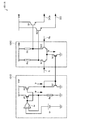
図1は、本実施形態の出力回路11の構成例を示す図である。出力回路11は後述する半導体集積回路10の出力段を構成し、非反転発振信号S、反転発振信号Sbに基づいて、PECL(Positive Emitter Coupled Logic)の差動出力信号である非反転出力信号DO、反転出力信号DObを出力する。なお、非反転発振信号S、反転発振信号Sbは本発明の入力制御信号に対応し、非反転出力信号DO、反転出力信号DObは本発明の出力信号に対応する。なお、以下において、非反転出力信号DOと反転出力信号DObとを区別する必要がない場合には、単に「出力回路11の出力信号」と表現する。
1. Output circuit, semiconductor integrated circuit [Configuration of output circuit]
FIG. 1 is a diagram illustrating a configuration example of the
出力回路11は、ドレイン端子に電源電圧Vddが印加され、ソース端子からそれぞれ非反転出力信号DO、反転出力信号DObを出力するMOS型の出力トランジスターN9、N10を含む。また、出力回路11は、第1の回路13、第2の回路14、第3の回路15を含む。出力トランジスターN9、N10は本発明の第1のトランジスターに対応する。
The
第1の回路13は、出力回路11の出力信号の第1の出力電圧V1、V2を生成する。第1の出力電圧V1、V2は、それぞれPECLの規格に基づく差動出力信号のハイレベル、ローレベルの電圧である。出力回路11の出力信号は、例えば製造ばらつきの影響によらず、第1の出力電圧V1または第1の出力電圧V2をとることが求められる。以下に、第1の回路13の構成について説明する。
The
図1のように、第1の回路13は、安定な基準電圧Vrを含む。基準電圧Vrは、例えばバンドギャップリファレンス回路等を用いて実現することができる。第1の回路13の誤差増幅器Arは、トランジスターP1のゲート電圧を調整して、反転入力端子と非反転入力端子の電圧がほぼ等しくなった状態で平衡を保つ。そのため、トランジスターP1に流れる電流Irは、トランジスターP1に接続された抵抗(以下、抵抗Rr)の抵抗値がRrであるとして、式(1)のように表すことができる。
As shown in FIG. 1, the
![]()
そして、図1のトランジスターP2はトランジスターP1と同じ形状であって、トランジスターP2にも電流Irが流れる。また、トランジスターP2に接続されたトランジスターN1とトランジスターN2とはカレントミラーを構成している。このとき、ミラー比は1であり、トランジスターN2にも電流Irが流れる。なお、ミラー比は1以外であってもよい。
![]()
The transistor P2 in FIG. 1 has the same shape as the transistor P1, and the current Ir also flows through the transistor P2. The transistors N1 and N2 connected to the transistor P2 form a current mirror. At this time, the mirror ratio is 1, and the current Ir flows through the transistor N2. The mirror ratio may be other than 1.
トランジスターN2に直列に接続された抵抗値がR1である抵抗(以下、抵抗R1)、抵抗値がR2である抵抗(以下、抵抗R2)に電流Irが流れるため電圧降下が発生する。すなわち、第1の回路13は、PECLの規格で定められたハイレベルの第1の出力電圧V1と、ローレベルの第1の出力電圧V2を生成する。第1の出力電圧V1、V2は以下の式(2)、式(3)で与えられる。
A voltage drop occurs because the current Ir flows through a resistor having a resistance value R1 (hereinafter referred to as a resistor R1) and a resistor having a resistance value R2 (hereinafter referred to as a resistor R2) connected in series to the transistor N2. That is, the
![]()
![]()
第1の出力電圧V1、V2は、電源電圧Vdd、安定な基準電圧Vrと抵抗Rr、抵抗R1、抵抗R2の抵抗比で定められるため、製造ばらつきに影響されることなく高い精度を得ることができる。つまり、抵抗Rr、抵抗R1、抵抗R2は同じようにばらつくため、これらの抵抗比で定められる第1の出力電圧V1、V2は製造ばらつきに影響されない。
![]()
![]()
The first output voltages V1 and V2 are determined by the power supply voltage Vdd, the stable reference voltage Vr and the resistance ratio of the resistors Rr, R1, and R2, so that high accuracy can be obtained without being affected by manufacturing variations. it can. That is, since the resistance Rr, the resistance R1, and the resistance R2 vary in the same manner, the first output voltages V1 and V2 determined by these resistance ratios are not affected by manufacturing variations.
次に、第2の回路14は、出力回路11の出力信号の出力電圧を複製する。そして、第1の出力電圧V1、V2と複製した出力電圧とに基づいて、出力トランジスターN9、N10のゲート電圧となる出力ゲート電圧VgH、VgLを生成する。つまり、第2の回路14は、出力トランジスターN9、N10(本発明の第1のトランジスターに対応)が出力電圧(本発明の第2の出力電圧に対応)を出力するために必要な出力ゲート電圧VgH、VgLを生成する。以下に、第2の回路14の構成について説明する。
Next, the
第2の回路14は、ハイレベルの第1の出力電圧V1、ローレベルの第1の出力電圧V2を第1の回路13から受け取る。そして、出力回路11の出力信号の出力電圧が第1の出力電圧V1となるような出力ゲート電圧VgHを生成する。また、出力回路11の出力信号の出力電圧が第1の出力電圧V2となるような出力ゲート電圧VgLも生成する。
The
例えば、出力トランジスターN9のゲート端子に出力ゲート電圧VgHが印加された場合、非反転出力信号DOの出力電圧は第1の出力電圧V1(信号レベルはハイレベル)になる。このとき、出力トランジスターN10のゲート端子には出力ゲート電圧VgLが印加されて、反転出力信号DObの出力電圧は第1の出力電圧V2(信号レベルはローレベル)になる。ここで、出力トランジスターN9、N10は同じ形状であるため、第2の回路14は、出力ゲート電圧VgH、VgLを出力トランジスターN9、N10のそれぞれについて生成する必要はない。
For example, when the output gate voltage VgH is applied to the gate terminal of the output transistor N9, the output voltage of the non-inverted output signal DO becomes the first output voltage V1 (the signal level is high). At this time, the output gate voltage VgL is applied to the gate terminal of the output transistor N10, and the output voltage of the inverted output signal DOb becomes the first output voltage V2 (the signal level is low). Here, since the output transistors N9 and N10 have the same shape, the
第2の回路14は、出力トランジスターN9および出力トランジスターN10を複製したレプリカ回路RE1、RE2を含む。レプリカ回路RE1、RE2によって、出力回路11の出力信号の出力電圧が複製される。レプリカ回路RE1は、出力ゲート電圧VgHを生成するために用いられ、レプリカ回路RE2は、出力ゲート電圧VgLを生成するために用いられる。
The
レプリカ回路RE1は、ドレイン端子に電源電圧Vddが印加されるレプリカトランジスターN3(本発明の第2のトランジスターに対応)と、レプリカトランジスターN3のソース端子に接続される電流源N4と、を含む。レプリカトランジスターN3は、出力トランジスターN9(および出力トランジスターN10)を複製している。また、電流源N4は、出力回路11の外部で付される負荷回路(図3(A)、図3(B)参照)を複製したものである。なお、本実施形態の電流源N4は、トランジスターを飽和状態で動作させたときの定電流を利用している。
The replica circuit RE1 includes a replica transistor N3 (corresponding to the second transistor of the present invention) to which the power supply voltage Vdd is applied to the drain terminal, and a current source N4 connected to the source terminal of the replica transistor N3. The replica transistor N3 duplicates the output transistor N9 (and the output transistor N10). The current source N4 is a copy of a load circuit (see FIGS. 3A and 3B) attached outside the
ここで、レプリカトランジスターN3は、出力トランジスターN9および出力トランジスターN10よりもサイズが小さい。サイズが小さいとは、具体的にはサイズ比、すなわち(ゲート幅/ゲート長)の比率が小さいことを意味する。例えば、レプリカトランジスターN3のゲート長L0(図4(A)、図4(B)参照)は、出力トランジスターN9および出力トランジスターN10と同じにする。一方、レプリカトランジスターN3のゲート幅W0(図4(A)、図4(B)参照)は、出力トランジスターN9および出力トランジスターN10よりも小さく設計し、サイズ比を例えば数十分の一程度にしてもよい。 Here, the replica transistor N3 is smaller in size than the output transistor N9 and the output transistor N10. The small size specifically means that the size ratio, that is, the ratio of (gate width / gate length) is small. For example, the gate length L0 (see FIGS. 4A and 4B) of the replica transistor N3 is the same as that of the output transistor N9 and the output transistor N10. On the other hand, the gate width W0 (see FIGS. 4A and 4B) of the replica transistor N3 is designed to be smaller than that of the output transistor N9 and the output transistor N10, and the size ratio is, for example, about several tenths. Also good.
このとき、出力トランジスターN9および出力トランジスターN10を複製したレプリカ回路RE1によって、正確に出力回路11の出力信号の出力電圧を複製できる一方で、レプリカ回路RE1の電流I1をサイズ比に応じて小さくすることが可能である。そのため、レプリカ回路RE1での消費電力を抑えることができる。
At this time, the replica circuit RE1 that replicates the output transistor N9 and the output transistor N10 can accurately replicate the output voltage of the output signal of the
第2の回路14は、ハイレベルをとる場合の出力回路11の出力信号の出力電圧を、レプリカトランジスターN3のソース端子の電圧(以下、ソース電圧VsH)によって複製できる。そして、第2の回路14は、ソース電圧VsHと第1の出力電圧V1との差を誤差増幅器A1で検出する。そして、図1のように、誤差増幅器A1の出力を、レプリカトランジスターN3のゲート電圧(本発明のレプリカトランジスター調整電圧)としている。ソース電圧VsHが誤差増幅器A1にフィードバックされることで、最終的にソース電圧VsHと第1の出力電圧V1が等しくなり、このときの誤差増幅器A1の出力(すなわち、レプリカトランジスター調整電圧)を出力ゲート電圧VgHとする。
The
このとき、出力ゲート電圧VgHがゲート端子に印加されたレプリカトランジスターN3のソース電圧VsHは、ハイレベルの第1の出力電圧V1に等しい。すると、レプリカ回路RE1は、出力トランジスターN9、出力トランジスターN10を複製したものであるから、ソース電圧VsHは、非反転出力信号DO、反転出力信号DObの出力電圧に対応する。そのため、出力ゲート電圧VgHが、出力トランジスターN9、N10のゲート端子に印加された場合、非反転出力信号DO、反転出力信号DObの出力電圧は第1の出力電圧V1に等しくなる。 At this time, the source voltage VsH of the replica transistor N3 to which the output gate voltage VgH is applied to the gate terminal is equal to the high-level first output voltage V1. Then, since the replica circuit RE1 is a replica of the output transistor N9 and the output transistor N10, the source voltage VsH corresponds to the output voltages of the non-inverted output signal DO and the inverted output signal DOb. Therefore, when the output gate voltage VgH is applied to the gate terminals of the output transistors N9 and N10, the output voltages of the non-inverted output signal DO and the inverted output signal DOb are equal to the first output voltage V1.
レプリカ回路RE2については、レプリカ回路RE1と同じ構造であるため説明を省略する。つまり、レプリカ回路RE1の説明における、レプリカトランジスターN3、電流源N4、電流I1、ソース電圧VsH、誤差増幅器A1、第1の出力電圧V1、出力ゲート電圧VgHを、それぞれ、レプリカトランジスターN5、電流源N6、電流I2、ソース電圧VsL、誤差増幅器A2、第1の出力電圧V2、出力ゲート電圧VgLに置き換えることでレプリカ回路RE2の説明になる。なお、レプリカトランジスターN5は本発明の第2のトランジスターに対応する。 Since the replica circuit RE2 has the same structure as the replica circuit RE1, the description thereof is omitted. That is, in the description of the replica circuit RE1, the replica transistor N3, the current source N4, the current I1, the source voltage VsH, the error amplifier A1, the first output voltage V1, and the output gate voltage VgH are respectively converted into the replica transistor N5 and the current source N6. , Current I2, source voltage VsL, error amplifier A2, first output voltage V2, and output gate voltage VgL are replaced with replica circuit RE2. The replica transistor N5 corresponds to the second transistor of the present invention.
なお、レプリカ回路RE2は、レプリカ回路RE1とは独立しており、例えば出力トランジスターN9および出力トランジスターN10とのサイズ比を異なるものとしてもよい。例えば、レプリカトランジスターN3のサイズ比が1/60であり、レプリカトランジスターN5のサイズ比が1/15であってもよい。 Note that the replica circuit RE2 is independent of the replica circuit RE1, and for example, the size ratio between the output transistor N9 and the output transistor N10 may be different. For example, the size ratio of the replica transistor N3 may be 1/60, and the size ratio of the replica transistor N5 may be 1/15.
そして、第3の回路15は、非反転発振信号S、反転発振信号Sbに基づいて出力ゲート電圧VgH、VgLの出力トランジスターN9、N10への印加を制御する。以下に、第3の回路15の構成について説明する。
The
図1のように、第3の回路15は、トランジスターP3、N7で構成される切替スイッチ(以下、第1の切替スイッチとする)と、トランジスターP4、N8で構成される切替
スイッチ(以下、第2の切替スイッチとする)を含む。第1の切替スイッチも第2の切替スイッチも出力ゲート電圧VgHまたは出力ゲート電圧VgLを出力する。
As shown in FIG. 1, the
第1の切替スイッチは、入力された非反転発振信号Sの信号レベルに応じて、出力トランジスターN9のゲート端子に出力ゲート電圧VgHまたは出力ゲート電圧VgLを印加する。また、第2の切替スイッチは、入力された反転発振信号Sbの信号レベルに応じて、出力トランジスターN10のゲート端子に出力ゲート電圧VgHまたは出力ゲート電圧VgLを印加する。 The first changeover switch applies the output gate voltage VgH or the output gate voltage VgL to the gate terminal of the output transistor N9 according to the signal level of the input non-inverted oscillation signal S. The second changeover switch applies the output gate voltage VgH or the output gate voltage VgL to the gate terminal of the output transistor N10 according to the signal level of the input inverted oscillation signal Sb.
このとき、非反転発振信号Sと反転発振信号Sbとは互いに異なる信号レベルを有し、例えば非反転発振信号Sがローレベルの場合、反転発振信号Sbはハイレベルである。この場合、出力トランジスターN9のゲート端子には出力ゲート電圧VgHが印加されて、非反転出力信号DOの出力電圧は第1の出力電圧V1に等しくなる。そして、出力トランジスターN10のゲート端子には出力ゲート電圧VgLが印加されて、反転出力信号DObの出力電圧は第1の出力電圧V2に等しくなる。ここで、第1の出力電圧V1、V2は、それぞれPECLの規格に基づく差動出力信号のハイレベル、ローレベルの電圧である。このように、出力回路11は入力制御信号(非反転発振信号S、反転発振信号Sb)に基づいて、PECLの差動出力信号を出力することができる。
At this time, the non-inverted oscillation signal S and the inverted oscillation signal Sb have different signal levels. For example, when the non-inverted oscillation signal S is at a low level, the inverted oscillation signal Sb is at a high level. In this case, the output gate voltage VgH is applied to the gate terminal of the output transistor N9, and the output voltage of the non-inverted output signal DO becomes equal to the first output voltage V1. Then, the output gate voltage VgL is applied to the gate terminal of the output transistor N10, and the output voltage of the inverted output signal DOb becomes equal to the first output voltage V2. Here, the first output voltages V1 and V2 are high-level and low-level voltages of the differential output signal based on the PECL standard, respectively. Thus, the
なお、本実施形態では、差動出力信号を出力するが、例えば反転出力信号DObを省略して、非反転出力信号DOからシングルエンド出力をしてもよい。このとき、トランジスターP4、N8で構成される第2の切替スイッチと反転発振信号Sbも省略される。 In this embodiment, a differential output signal is output. However, for example, the inverted output signal DOb may be omitted and a single-ended output may be output from the non-inverted output signal DO. At this time, the second changeover switch including the transistors P4 and N8 and the inverted oscillation signal Sb are also omitted.
[半導体集積回路の構成]
図2は、出力回路11と発振回路12とを含む半導体集積回路10を、水晶振動子26(本発明の発振素子に対応)と接続した状態を示す図である。図2のように出力回路11は半導体集積回路10の出力段として用いられる。なお、図1と同じ要素については同じ符号を付しており説明を省略する。
[Configuration of semiconductor integrated circuit]
FIG. 2 is a diagram showing a state where the semiconductor integrated
出力回路11は、水晶振動子26を発振させて発振信号(ここでは、非反転発振信号Sおよび反転発振信号Sb)を生成する発振回路12とともに1チップ化されて、半導体集積回路10を構成している。また、半導体集積回路10は、水晶振動子26と接続されて、温度補償や温度制御をしていない水晶発振器20、すなわちSPXO(Simple Packaged Crystal Oscillator)を構成する。
The
発振回路12は、アナログ増幅器として機能する帰還抵抗Rfを備えたインバーター24と、固定容量41、42を含む。そして、図2に示すように水晶振動子26と接続されて発振ループを形成している。また、発振回路12はインバーター25を含み、発振信号として非反転発振信号Sだけでなく反転発振信号Sbも出力する。出力回路11は、これらの信号を受け取り、PECLの差動出力信号である非反転出力信号DO、反転出力信号DObを出力する。
The
ここで、PECLの差動出力には終端回路が付加される。図3(A)、図3(B)はその終端回路を説明するための図である。図3(A)、図3(B)に示すように、本実施形態の出力回路11を含む半導体集積回路10は、その外部で終端回路が付加される。
Here, a termination circuit is added to the differential output of PECL. 3A and 3B are diagrams for explaining the termination circuit. As shown in FIGS. 3A and 3B, the semiconductor integrated
PECLは、ECL(Emitter Coupled Logic)とは異なり負電源を必要とせず、正の電圧であるVdd−2V(電源電圧Vddよりも2V低い電圧)を終端電圧として用いる。そして、図3(B)のように、この終端電圧に対して50Ωで終端を行うことが求められている。
Unlike ECL (Emitter Coupled Logic), PECL does not require a negative power supply, and uses a positive voltage Vdd-2V (a
しかし、終端電圧としてVdd−2Vを別途用意せずに、図3(A)のようなテブナン終端回路が用いられることが多い。このとき、抵抗値Rp、Rnを以下の式(4)、式(5)を満たすように設定することで、図3(B)と電気特性を同じにすることができる。 However, a Thevenin termination circuit as shown in FIG. 3A is often used without separately preparing Vdd-2V as the termination voltage. At this time, by setting the resistance values Rp and Rn to satisfy the following formulas (4) and (5), the electrical characteristics can be made the same as those in FIG.
![]()
![]()
[従来の出力回路との比較]
ここで、本実施形態の出力回路11が以上のように半導体集積回路10の出力段として使用されることを前提として、従来の出力回路1011A、1011Bとの比較を行う。図9は、従来の出力回路1011Aを表す回路図である。出力回路1011Aは、出力トランジスターとしてNPNトランジスターQ1、Q2を用いている。なお、図1〜図3(B)と同じ要素には同じ符号を付しており説明を省略する。
![]()
![]()
[Comparison with conventional output circuit]
Here, on the assumption that the
出力回路1011Aは、前段回路1013と後段回路1015を含む。前段回路1013は、本実施形態の出力回路11の第1の回路13に対応するが、第1の出力電圧V1、V2を生成する回路(抵抗R1、抵抗R2、トランジスターN2で構成される回路)を含まない。
The
後段回路1015のトランジスターN13は、前段回路1013のトランジスターN1とカレントミラーを構成している。トランジスターN13には電流Isが流れるが、式(1)のIrを用いて、Is=n×Irとなる。ここで、nはミラー比であって、トランジスターN1とトランジスターN13のゲート幅の比で定まる。なお、ゲート長は同じであるとする。
The transistor N13 of the
後段回路1015のトランジスターN11、N12はスイッチとして機能する。トランジスターN11、N12のゲート端子には、それぞれ非反転発振信号S、反転発振信号Sb(図2参照)が入力される。非反転発振信号Sと反転発振信号Sbは差動信号であるから、トランジスターN11、N12は交互にオン、オフを繰り返す。
Transistors N11 and N12 of the
このとき、出力回路1011AのNPNトランジスターQ1、Q2のベース電圧が変化するので、出力回路1011Aの出力信号(非反転出力信号DO、反転出力信号DOb)にはハイレベルとローレベルの出力電圧が交互に現れる。ここで、ハイレベルの出力電圧をVoH、ローレベルの出力電圧をVoLとする。VoH、VoLは、後段回路1015が抵抗値Rsの抵抗を含むとして、それぞれ式(6)、式(7)で表される。
At this time, since the base voltages of the NPN transistors Q1 and Q2 of the
![]()
![]()
![]()
![]()
![]()
![]()
![]()
![]()
ここで、式(8)、式(9)をもとに、出力回路1011Aの出力信号(非反転出力信号DO、反転出力信号DOb)の出力電流について検討する。図3(B)のように、Vdd−2Vの終端電圧に対して50Ωのインピーダンスで終端されるため、ハイレベルの出力電流であるIoH、ローレベルの出力電流であるIoLは、それぞれ式(10)、式(11)の範囲であることが求められる。
Here, based on Expressions (8) and (9), the output current of the output signals (non-inverted output signal DO and inverted output signal DOb) of the
![]()
![]()
![]()
![]()
従来の出力回路1011Aは、抵抗値Rs、電流Is、ベース−エミッタ間電圧であるVbeH、VbeLを調整することで、PECLの規格を表す式(8)、式(9)を満たすことができる。しかし、出力トランジスターとしてNPNトランジスターQ1、Q2を用いるため、BiCMOSプロセスで製造する必要がある。そのため、MOSプロセスに比べてプロセスコストが高くなり、結果的に、出力回路1011Aを含む集積回路装置のコストが上昇してしまう。
The
そこで、図10のように、出力回路1011AのNPNトランジスターQ1、Q2をMOS型の出力トランジスターN9、N10に置き換えた出力回路1011Bを用いることが考えられる。出力回路1011Bは、出力回路1011Aとは異なる従来回路であって、MOS型のトランジスターのみで構成されており、安価なMOSプロセスで製造することが可能である。なお、前段回路1013、後段回路1015については図9と同じであり、説明を省略する。
Therefore, as shown in FIG. 10, it is conceivable to use an
しかし、出力回路1011Bでは、PECLの規格で求められるVoH、VoLの範囲(式(8)、式(9))を満たすことが難しい。出力回路1011Bにおけるハイレベルの出力電圧であるVoH、ローレベルの出力電圧であるVoLは、それぞれ式(12)、式(13)で表される。
However, it is difficult for the
![]()
![]()
![]()
![]()
しかし、MOS型のトランジスターのVgsH、VgsLは、閾値電圧Vthとオーバードライブ電圧の和で与えられる。閾値電圧Vthは製造ばらつきが大きく、例えば±0.1V程度のばらつきを見込む必要がある。すると、閾値電圧Vthのばらつきが、式(8)、式(9)に示された許容される変動幅を超えてしまうため、出力回路1011BはPECLの規格を満たすことができない。
However, VgsH and VgsL of the MOS transistor are given by the sum of the threshold voltage Vth and the overdrive voltage. The threshold voltage Vth has a large manufacturing variation. For example, it is necessary to allow a variation of about ± 0.1V. Then, the variation of the threshold voltage Vth exceeds the allowable fluctuation range shown in the equations (8) and (9), and thus the
このとき、閾値電圧Vthのばらつきが許容される変動幅におさまるように出力回路1011Bの良品選別を行う、あるいは製造装置を限定して閾値電圧Vthのばらつきを小さくする、などの対策が考えられる。しかし、どちらの対策も製造コストの上昇を招き、MOSプロセスで製造することによるコスト低減の利益が失われる。
At this time, it is possible to take measures such as selecting non-defective products of the
さらに、出力回路1011Bにおいて、出力トランジスター(出力トランジスターN9、出力トランジスターN10)の閾値電圧Vthは、基板バイアス効果によっても変動する。基板バイアス効果は、ソース−バルク間電圧が高いほど閾値電圧Vthが増加する現象であり、MOS型トランジスターに特有の現象である。図10のように、出力トランジスター(出力トランジスターN9、出力トランジスターN10)のソース端子の電圧は、ハイレベルの出力電圧VoH、または、ローレベルの出力電圧VoLのいずれかに当たるが、VoH、VoLは式(12)、式(13)のように電源電圧Vddに依存している。このため、電源電圧Vddによっても閾値電圧Vthは変動してしまう。よって、出力回路1011Bを複数の電源電圧(例えば、2.5Vおよび3.3V)で使用するとした場合、それぞれの電源電圧に対して式(8)、式(9)を満たすことは非常に困難である。そのため、電源電圧の選択に関して、使用範囲が限定されていた。
Further, in the
また、閾値電圧Vthは温度によっても変動する。閾値電圧Vthは、高温であるほど低下する傾向がある。そのため、式(8)、式(9)を満たすには、例えば特定の温度の近傍だけで出力回路1011Bを動作させなければならないといった制限が生じることになる。
The threshold voltage Vth also varies depending on the temperature. The threshold voltage Vth tends to decrease as the temperature increases. Therefore, in order to satisfy the expressions (8) and (9), for example, there is a restriction that the
以上のように、従来の出力回路1011Bは、MOSプロセスで製造することは可能であっても、閾値電圧VthがPVT変動、すなわちプロセス(製造ばらつき)の変動、電圧(基板バイアス効果)の変動、および温度の変動の影響を受ける。そのため、式(8)、式(9)を満たすことが困難であり、出力回路1011Bの使用は現実的ではなかった。
As described above, the
ここで、再び図1を参照して、本実施形態の出力回路11について説明する。出力回路11の第1の回路13は第1の出力電圧V1、V2を生成する。第1の出力電圧V1、V2は、式(2)、式(3)のように安定な基準電圧Vrと、抵抗Rr、抵抗R1、抵抗R
2の抵抗比によって定めることができる。
Here, the
2 resistance ratio.
第1の回路13は、式(8)、式(9)に示されるVoH、VoLの中心の値を第1の出力電圧V1、V2とすることができる。例えば、基準電圧Vr=1.25Vである場合、R1/Rr=0.762、R2/Rr=0.61とする。このとき、第1の出力電圧V1=Vdd−0.9525V、第1の出力電圧V2=Vdd−1.715Vとすることができる。このとき、抵抗Rr、抵抗R1、抵抗R2の抵抗比で第1の出力電圧V1、V2を定めているため、例えば製造ばらつきに影響されず、高い精度を得ることができる。
The
また、出力回路11の第2の回路14は、レプリカ回路RE1、RE2によって出力回路11の出力信号の出力電圧を複製する。そして、第1の出力電圧V1、V2と複製した出力電圧とを誤差増幅器A1、A2で一致させて、出力トランジスターN9、N10のゲート電圧となる出力ゲート電圧VgH、VgLを生成する。
Further, the
ここで、レプリカ回路RE1、RE2に含まれるレプリカトランジスターN3、N5は、出力回路11のMOS型の出力トランジスター(出力トランジスターN9、N10)を正確に複製している。そのため、出力回路11のMOS型の出力トランジスターのPVT変動はレプリカトランジスターN3、N5にも同じく影響する。したがって、出力回路11は、出力信号の出力電圧を常に第1の出力電圧V1または第1の出力電圧V2とすることができるので、式(8)、式(9)を満たし、PECL出力回路として使用できる。
Here, the replica transistors N3 and N5 included in the replica circuits RE1 and RE2 accurately duplicate the MOS type output transistors (output transistors N9 and N10) of the
なお、前記のようにレプリカトランジスターN3、N5は、出力回路11の出力トランジスターよりもサイズを小さくして、出力回路11の消費電力を抑えている。つまり、レプリカトランジスターN3、N5は、出力回路11の出力トランジスターと同じサイズではない。そのため、以下に説明するようなレイアウトを行うことが好ましい。
As described above, the replica transistors N3 and N5 are made smaller in size than the output transistors of the
例えば、図4(A)のように出力トランジスターN9、N10がレイアウトされているとする。ここで、図4(A)のSRはソースであり、DRはドレインである。またゲートGTについて、ゲート長はL0であり、ゲート幅はW0の整数倍(ここでは、整数Mを用いてM×W0とする)である。 For example, assume that output transistors N9 and N10 are laid out as shown in FIG. Here, SR in FIG. 4A is a source, and DR is a drain. For the gate GT, the gate length is L0, and the gate width is an integral multiple of W0 (here, the integer M is used as M × W0).
このとき、図4(B)のようにレプリカトランジスターN3、N5をレイアウトする。レプリカトランジスターN3、N5のゲート長は同じくL0であるが、ゲート幅はW0であって、出力トランジスターN9、N10と比較してサイズ比が1/Mである。つまり、レプリカトランジスターN3、N5は、図4(B)の枠で囲った1つのトランジスターだけであり、その他はトランジスターとして使用されない。しかし、レプリカトランジスターN3、N5は、不使用部分も含めて出力トランジスターN9、N10のレイアウトを複製することで、PVT変動の影響までも正確に反映する。 At this time, the replica transistors N3 and N5 are laid out as shown in FIG. The gate lengths of the replica transistors N3 and N5 are also L0, but the gate width is W0 and the size ratio is 1 / M compared to the output transistors N9 and N10. That is, the replica transistors N3 and N5 are only one transistor surrounded by a frame in FIG. 4B, and the other transistors are not used as transistors. However, the replica transistors N3 and N5 accurately reflect even the influence of the PVT variation by duplicating the layout of the output transistors N9 and N10 including the unused portion.
また、レプリカ回路RE1、RE2は、出力回路11の外部で付される負荷回路(図3(A)、図3(B)参照)を複製するのに、電流源N4、N6を用いている。ここで、式(10)、式(11)のようにIoH、IoLは電源電圧Vddに依存しない。そのため、電流I1、I2によって、IoH、IoLを複製するレプリカ回路RE1、RE2を用いることで、電源電圧が変わっても式(8)、式(9)を満たすことができる。すなわち、出力回路11は、電源電圧を限定することなく、使用範囲を広げることができる。
The replica circuits RE1 and RE2 use current sources N4 and N6 to replicate a load circuit (see FIGS. 3A and 3B) attached outside the
なお、レプリカ回路RE1、RE2の電流I1、I2には高い精度は求められない。電流I1は、IoHの所望の電流値である20.95mA(式(10)参照)の例えば1/60である0.35mAをターゲットにしてもよい。また、電流I2は、IoLの所望の電流値である5.7mA(式(11)参照)の例えば1/15である0.38mAをター
ゲットにしてもよい。電流I1、I2の電流値がターゲットからずれると、レプリカトランジスターN3、N5のオーバードライブ電圧にもずれが生じる。しかし、出力トランジスターN9、N10のゲート幅を十分大きくとれば、VgsH、VgsLは、閾値電圧Vthが支配的であるためオーバードライブ電圧のずれは無視できる。そのため、電流I1、I2には高い精度は求められない。
Note that high accuracy is not required for the currents I1 and I2 of the replica circuits RE1 and RE2. The current I1 may be targeted to 0.35 mA, which is, for example, 1/60 of 20.95 mA (see Equation (10)), which is a desired current value of IoH. Further, the current I2 may be targeted to 0.38 mA, for example, 1/15 of 5.7 mA (refer to Expression (11)) which is a desired current value of IoL. When the current values of the currents I1 and I2 deviate from the target, the overdrive voltages of the replica transistors N3 and N5 also deviate. However, if the gate widths of the output transistors N9 and N10 are sufficiently large, since the threshold voltage Vth is dominant in VgsH and VgsL, the deviation of the overdrive voltage can be ignored. Therefore, high accuracy is not required for the currents I1 and I2.
以上のように、本実施形態の出力回路11は、従来の出力回路1011Aと異なり安価なMOSプロセスで製造可能であり、従来の出力回路1011Bと異なりPVT変動の影響で出力電圧が第1の出力電圧V1、V2から大きく外れる問題もない。つまり、本実施形態の出力回路11は、MOS型の出力トランジスターを用いながらも、例えば製造ばらつきといったPVT変動の影響によらず、所望の出力電圧にすることができる。また、本実施形態の出力回路11は、電源電圧を限定することなく、使用範囲を広げることができる。
As described above, the
2.振動デバイス
本実施形態の振動デバイス200は、出力回路211、発振回路212、発振回路212により発振する発振素子230を含むものである。出力回路211と発振回路212とは、半導体集積回路210として振動デバイス200に含まれていてもよい。本実施形態の振動デバイス200の説明において、出力回路211は図1、図2の出力回路11が対応し、発振回路212は図2の発振回路12が対応し、半導体集積回路210は図2〜図3(B)の半導体集積回路10が対応する。なお、後述する温度補償型発振器の発振回路212は、図2の発振回路12の構成に加えて温度補償を行う回路を含んでいるものとする。
2. Vibration Device The
振動デバイス200としては、例えば、発振素子230として振動子を備えた発振器や発振素子230として振動型のセンサー素子240を備えた物理量センサー等が挙げられる。
Examples of the
図5(A)に、振動デバイス200の一例である発振器の構成例を示す。図5(A)に示す振動デバイス200(発振器)は、温度補償型発振器であり、出力回路211と、発振回路212と、温度センサー220と、発振素子230とを含む。ここで、出力回路211、発振回路212は、半導体集積回路210を構成していてもよい。
FIG. 5A illustrates a configuration example of an oscillator that is an example of the
発振回路212は、温度センサー220の出力に応じた周波数制御電圧Vcを内部で生成することで、温度変化に応じて可変容量素子の容量値を変化させ、発振素子230(例えば、図2〜図3(B)の水晶振動子26が対応)の周波数温度特性を補償しながら一定の周波数で発振させる。そして、得られた発振信号は出力回路211によってクロック信号として出力される。ここで、出力回路211は差動信号であるクロック信号を出力してもよい(図1参照)。
The
本実施形態の振動デバイスである発振器としては、温度補償型発振器の他にも、電圧制御型発振器(VCXOやVCSO等)、電圧制御温度補償型発振器(VC−TCXO)、恒温型発振器(OCXO等)等が挙げられる。また、温度センサー220を含まず、温度補償を行わないSPXOであってもよい。つまり、図2の水晶発振器20は振動デバイス200の一例である。
As an oscillator which is a vibration device of the present embodiment, in addition to a temperature compensated oscillator, a voltage controlled oscillator (VCXO, VCSO, etc.), a voltage controlled temperature compensated oscillator (VC-TCXO), a constant temperature oscillator (OCXO, etc.) ) And the like. Further, it may be an SPXO that does not include the
図5(B)に、振動デバイスの一例である物理量センサーの構成例を示す。図5(B)に示す振動デバイス200(物理量センサー)は、出力回路211と、発振回路212と、温度センサー220と、水晶等を材料とするセンサー素子240と、検出回路250とを含む。ここで、出力回路211、発振回路212、検出回路250は、半導体集積回路
210を構成していてもよい。
FIG. 5B illustrates a configuration example of a physical quantity sensor that is an example of a vibration device. A vibration device 200 (physical quantity sensor) illustrated in FIG. 5B includes an
発振回路212は、温度センサー220の出力に応じた周波数制御電圧Vcを内部で生成することで、温度変化に応じて可変容量素子の容量値を変化させ、センサー素子240の周波数温度特性を補償しながら一定の周波数で発振させる。
The
センサー素子240は、一定の周波数で振動しながら、加わった物理量(例えば、角速度や加速度等)の大きさに応じた検出信号を出力する。
The
検出回路250は、センサー素子240の検出信号の検波や直流化を行い、センサー素子240に加わった物理量の大きさに応じた信号レベルの物理量信号を生成する。そして、生成された物理量信号は出力回路211によって出力される。ここで、出力回路211は差動信号である物理量信号を出力してもよい(図1参照)。
The
なお、検出回路250は、温度センサー220の出力に応じて、回路素子の温度特性やセンサー素子240の温度特性を補償し、物理量信号の振動レベルを調整するようにしてもよい。
The
本実施形態の振動デバイスである物理量センサーとしては、角速度センサー(ジャイロセンサー)や加速度センサー等が挙げられる。 Examples of the physical quantity sensor that is the vibration device of the present embodiment include an angular velocity sensor (gyro sensor) and an acceleration sensor.
本実施形態によれば、振動デバイス200は、半導体集積回路210の出力回路211を用いてクロック信号、物理量信号等を出力する。そのため、製造ばらつきの影響によらずに所望の出力電圧のクロック信号、物理量信号等を出力することが可能である。
According to the present embodiment, the
3.電子機器
本実施形態の電子機器300について、図6〜図7を用いて説明する。なお、図1〜図5と同じ要素については同じ番号、符号を付しており説明を省略する。
3. Electronic Device An
図6は、電子機器300の機能ブロック図である。電子機器300は、半導体集積回路210と発振素子230とを含む振動デバイス200、CPU(Central Processing Unit)320、操作部330、ROM(Read Only Memory)340、RAM(Random Access
Memory)350、通信部360、表示部370、音出力部380を含んで構成されている。なお、電子機器300は、図6の構成要素(各部)の一部を省略又は変更してもよいし、他の構成要素を付加した構成としてもよい。
FIG. 6 is a functional block diagram of the
Memory) 350,
振動デバイス200は、半導体集積回路210と発振素子230とが接続された発振器に対応する(図5(A)参照)。なお、図6では温度センサー220の図示を省略している。振動デバイス200は、半導体集積回路210が含む出力回路211からのクロック信号をCPU320だけでなく各部に供給する(図示は省略)。
The
CPU320は、ROM340等に記憶されているプログラムに従い、振動デバイス200が出力するクロック信号を用いて各種の計算処理や制御処理を行う。具体的には、CPU320は、操作部330からの操作信号に応じた各種の処理、外部とデータ通信を行うために通信部360を制御する処理、表示部370に各種の情報を表示させるための表示信号を送信する処理、音出力部380に各種の音を出力させる処理等を行う。
The
操作部330は、操作キーやボタンスイッチ等により構成される入力装置であり、ユーザーによる操作に応じた操作信号をCPU320に出力する。
The
ROM340は、CPU320が各種の計算処理や制御処理を行うためのプログラムやデータ等を記憶している。
The
RAM350は、CPU320の作業領域として用いられ、ROM340から読み出されたプログラムやデータ、操作部330から入力されたデータ、CPU320が各種プログラムに従って実行した演算結果等を一時的に記憶する。
The
通信部360は、CPU320と外部装置との間のデータ通信を成立させるための各種制御を行う。
The
表示部370は、LCD(Liquid Crystal Display)等により構成される表示装置であり、CPU320から入力される表示信号に基づいて各種の情報を表示する。
The
そして、音出力部380は、スピーカー等の音を出力する装置である。
The
電子機器300は、半導体集積回路210が含む出力回路211からのクロック信号を受け取るので、製造ばらつきの影響によらない所望の出力電圧のクロック信号を利用できる。そのため、電子機器300は、動作の信頼性を高めることができる。
Since the
電子機器300としては種々が考えられる。例えば、ネットワークサーバー、パーソナルコンピューター(例えば、モバイル型パーソナルコンピューター、ラップトップ型パーソナルコンピューター、タブレット型パーソナルコンピューター)、携帯電話機などの移動体端末、ディジタルスチールカメラ、インクジェット式吐出装置(例えば、インクジェットプリンター)、ルーターやスイッチなどのストレージエリアネットワーク機器、ローカルエリアネットワーク機器、テレビ、ビデオカメラ、ビデオテープレコーダー、カーナビゲーション装置、ページャー、電子手帳(通信機能付も含む)、電子辞書、電卓、電子ゲーム機器、ゲーム用コントローラー、ワードプロセッサー、ワークステーション、テレビ電話、防犯用テレビモニター、電子双眼鏡、POS端末、医療機器(例えば電子体温計、血圧計、血糖計、心電図計測装置、超音波診断装置、電子内視鏡)、魚群探知機、各種測定機器、計器類(例えば、車両、航空機、船舶の計器類)、フライトシュミレーター、ヘッドマウントディスプレイ、モーショントレース、モーショントラッキング、モーションコントローラー、PDR(歩行者位置方位計測)等が挙げられる。
Various
図7は、電子機器300の一例であるネットワークサーバーの外観の一例を示す図である。電子機器300であるネットワークサーバーは、表示部370としてLCDを備えている。そして、電子機器300であるネットワークサーバーは、半導体集積回路210が含む出力回路211からのクロック信号を受け取るので、製造ばらつきの影響によらない所望の出力電圧のクロック信号を利用できる。そのため、ネットワークサーバーは、動作の信頼性を高めることができる。
FIG. 7 is a diagram illustrating an example of the appearance of a network server that is an example of the
4.移動体
本実施形態の移動体400について、図8を用いて説明する。
4). Mobile Object A
図8は、本実施形態の移動体400の一例を示す図(上面図)である。図8に示す移動体400は、発振部410、エンジンシステム、ブレーキシステム、キーレスエントリーシステム等の各種の制御を行うコントローラー420、430、440、バッテリー450、バックアップ用バッテリー460を含んで構成されている。なお、本実施形態の移動体は、図8の構成要素(各部)の一部を省略又は変更してもよいし、他の構成要素を付加した構成としてもよい。
FIG. 8 is a diagram (top view) illustrating an example of the moving
発振部410は、半導体集積回路210を含む振動デバイス200(発振器)に対応する。その他の構成要素の詳細な説明は省略するが、移動体の移動に必要な制御を行うため高い信頼性が要求される。例えば、バッテリー450の他に、バックアップ用バッテリー460を備えることで信頼性を高めている。
The
ここで、移動体400のシステムは、発振部410すなわち半導体集積回路210を含む振動デバイス200(発振器)からの、製造ばらつきの影響によらない所望の出力電圧のクロック信号を利用できる。よって、移動体400は、システムの動作についても信頼性を高めることができる。
Here, the system of the moving
なお、このような移動体400としては種々の移動体が考えられ、例えば、自動車(電気自動車も含む)、ジェット機やヘリコプター等の航空機、船舶、ロケット、人工衛星等が挙げられる。
In addition, various moving bodies can be considered as such a moving
5.その他
本発明は、前記の実施形態で説明した構成と実質的に同一の構成(例えば、機能、方法および結果が同一の構成、あるいは目的および効果が同一の構成)を含む。また、本発明は、実施形態で説明した構成の本質的でない部分を置き換えた構成を含む。また、本発明は、実施形態で説明した構成と同一の作用効果を奏する構成又は同一の目的を達成することができる構成を含む。また、本発明は、実施形態で説明した構成に公知技術を付加した構成を含む。
5. Others The present invention includes substantially the same configuration (for example, a configuration having the same function, method and result, or a configuration having the same purpose and effect) as the configuration described in the above embodiment. In addition, the invention includes a configuration in which a non-essential part of the configuration described in the embodiment is replaced. In addition, the present invention includes a configuration that exhibits the same operational effects as the configuration described in the embodiment or a configuration that can achieve the same object. In addition, the invention includes a configuration in which a known technique is added to the configuration described in the embodiment.
10 半導体集積回路、11 出力回路、12 発振回路、13 第1の回路、14 第2の回路、15 第3の回路、20 水晶発振器、24 インバーター、25 インバーター、26 水晶振動子、41 固定容量、42 固定容量、200 振動デバイス、210 半導体集積回路、211 出力回路、212 発振回路、220 温度センサー、230 発振素子、240 センサー素子、250 検出回路、300 電子機器、320 CPU、330 操作部、340 ROM、350 RAM、360 通信部、370 表示部、380 音出力部、400 移動体、410 発振部、420 コントローラー、450 バッテリー、460 バックアップ用バッテリー、1011A:出力回路、1011B:出力回路、1013 前段回路、1015 後段回路、A1 誤差増幅器、A2 誤差増幅器、Ar 誤差増幅器、DO 非反転出力信号、DOb 反転出力信号、GT ゲート、I1 電流、I2 電流、Ir 電流、Is 電流、L0 ゲート長、N1 トランジスター、N2 トランジスター、N3 レプリカトランジスター、N4 電流源、N5 レプリカトランジスター、N6 電流源、N9 出力トランジスター、N10 出力トランジスター、N11 トランジスター、N13 トランジスター、P1 トランジスター、P2 トランジスター、P3 トランジスター、P4 トランジスター、Q1 NPNトランジスター、Q2 NPNトランジスター、R1 抵抗、R2 抵抗、RE1 レプリカ回路、RE2 レプリカ回路、Rf 帰還抵抗、Rr 抵抗、S 非反転発振信号、Sb 反転発振信号、V1 第1の出力電圧、V2 第1の出力電圧、Vc 周波数制御電圧、Vdd 電源電圧、VgH 出力ゲート電圧、VgL 出力ゲート電圧、Vr 基準電圧、VsH ソース電圧、VsL ソース電圧、Vth 閾値電圧、W0 ゲート幅 DESCRIPTION OF SYMBOLS 10 Semiconductor integrated circuit, 11 Output circuit, 12 Oscillator circuit, 13 1st circuit, 14 2nd circuit, 15 3rd circuit, 20 Crystal oscillator, 24 Inverter, 25 Inverter, 26 Crystal oscillator, 41 Fixed capacity | capacitance, 42 fixed capacity, 200 vibration device, 210 semiconductor integrated circuit, 211 output circuit, 212 oscillation circuit, 220 temperature sensor, 230 oscillation element, 240 sensor element, 250 detection circuit, 300 electronic device, 320 CPU, 330 operation unit, 340 ROM 350 RAM, 360 communication unit, 370 display unit, 380 sound output unit, 400 moving body, 410 oscillation unit, 420 controller, 450 battery, 460 backup battery, 1011A: output circuit, 1011B: output circuit, 1013 pre-stage circuit, 10 5 Subsequent circuit, A1 error amplifier, A2 error amplifier, Ar error amplifier, DO non-inverted output signal, DOb inverted output signal, GT gate, I1 current, I2 current, Ir current, Is current, L0 gate length, N1 transistor, N2 Transistor, N3 replica transistor, N4 current source, N5 replica transistor, N6 current source, N9 output transistor, N10 output transistor, N11 transistor, N13 transistor, P1 transistor, P2 transistor, P3 transistor, P4 transistor, Q1 NPN transistor, Q2 NPN Transistor, R1 resistor, R2 resistor, RE1 replica circuit, RE2 replica circuit, Rf feedback resistor, Rr resistor, S non-inverted oscillation signal, Sb Inverted oscillation signal, V1 first output voltage, V2 first output voltage, Vc frequency control voltage, Vdd power supply voltage, VgH output gate voltage, VgL output gate voltage, Vr reference voltage, VsH source voltage, VsL source voltage, Vth Threshold voltage, W0 gate width
Claims (11)
基準電圧を基にして抵抗比で定められる第1の出力電圧を生成する第1の回路と、
前記第1の出力電圧と、前記出力信号の第2の出力電圧を設定することが可能な第2のトランジスターのソース電圧と、を比較して、前記第1のトランジスターが前記第2の出力電圧を出力するために必要な出力ゲート電圧を生成する第2の回路と、
前記出力ゲート電圧を前記第1のトランジスターへ印加するタイミングを、入力制御信号に基づいて制御する第3の回路と、
を含む出力回路。 An output circuit having a MOS-type first transistor that outputs a power signal from a source terminal when a power supply voltage is applied to a drain terminal,
A first circuit for generating a first output voltage determined by a resistance ratio based on a reference voltage;
Comparing the first output voltage with a source voltage of a second transistor capable of setting a second output voltage of the output signal, the first transistor has the second output voltage. A second circuit for generating an output gate voltage necessary for outputting
A third circuit for controlling the timing of applying the output gate voltage to the first transistor based on an input control signal;
Including output circuit.
前記第2のトランジスターは、
ドレイン端子に電源電圧が印加され、
前記第2の回路は、
前記第2のトランジスターのソース端子に接続される電流源を含み、
前記第2のトランジスターのソース端子の電圧と、前記第2の出力電圧とが一致するように、前記第2のトランジスターのゲート電圧を生成し、
前記第2のトランジスターの前記ゲート電圧を前記出力ゲート電圧とする出力回路。 The output circuit according to claim 1,
The second transistor is:
A power supply voltage is applied to the drain terminal ,
The second circuit includes:
A current source connected to the source terminal of the second transistor;
The voltage of the source terminal of the second transistor, such that the second output voltage are matched to generate a gate voltage of said second transistor,
An output circuit using the gate voltage of the second transistor as the output gate voltage.
前記第2のトランジスターは、ドレイン端子に電源電圧が印加され、ソース端子に電流源が接続された前記第1のトランジスターのレプリカトランジスターであって、
前記第2の回路は、
前記レプリカトランジスターのソース端子の電圧と、前記第2の出力電圧とが一致するように、前記レプリカトランジスターのゲート電圧であるレプリカトランジスター調整電圧を生成し、
前記レプリカトランジスター調整電圧を前記出力ゲート電圧とする出力回路。 The output circuit according to claim 1,
The second transistor is a replica transistor of the first transistor in which a power supply voltage is applied to a drain terminal and a current source is connected to a source terminal,
The second circuit includes:
Generating a replica transistor adjustment voltage, which is a gate voltage of the replica transistor, so that a voltage of a source terminal of the replica transistor matches the second output voltage;
An output circuit using the replica transistor adjustment voltage as the output gate voltage.
前記第2のトランジスターは、
前記第1のトランジスターよりもサイズが小さい出力回路。 The output circuit according to any one of claims 1 to 3 ,
The second transistor is:
The first of the output circuit have smaller in size than the transistor.
前記出力信号は、信号レベルとして第1のレベル、および前記第1のレベルと異なる第2のレベルをとり、
前記第1の回路は、
前記第1のレベル、前記第2のレベルのそれぞれに対応する前記第1の出力電圧を生成し、
前記第2の回路は、
前記第1のレベル、前記第2のレベルのそれぞれに対応する前記出力ゲート電圧である第1の出力ゲート電圧、第2の出力ゲート電圧を生成し、
前記第3の回路は、
前記入力制御信号に基づいて、前記第1の出力ゲート電圧および前記第2の出力ゲート電圧の一方を選択して前記第1のトランジスターに印加する出力回路。 The output circuit according to any one of claims 1 to 4,
The output signal takes a first level as a signal level and a second level different from the first level,
The first circuit includes:
Generating the first output voltage corresponding to each of the first level and the second level;
The second circuit includes:
Generating a first output gate voltage and a second output gate voltage that are the output gate voltages corresponding to each of the first level and the second level;
The third circuit includes:
An output circuit that selects one of the first output gate voltage and the second output gate voltage based on the input control signal and applies the selected one to the first transistor.
前記出力信号は複数である出力回路。 The output circuit according to any one of claims 1 to 5,
An output circuit having a plurality of the output signals.
前記出力信号は差動出力である出力回路。 The output circuit according to claim 6.
An output circuit in which the output signal is a differential output.
発振素子を発振させて発振信号を生成する発振回路と、
を含み、
前記出力回路は、
前記発振信号を前記入力制御信号とする半導体集積回路。 An output circuit according to any one of claims 1 to 7,
An oscillation circuit for generating an oscillation signal by oscillating an oscillation element;
Including
The output circuit is
A semiconductor integrated circuit using the oscillation signal as the input control signal.
前記発振素子と、
を含む振動デバイス。 A semiconductor integrated circuit according to claim 8,
The oscillation element;
Including vibration device.
Priority Applications (3)
| Application Number | Priority Date | Filing Date | Title |
|---|---|---|---|
| JP2013063668A JP6094747B2 (en) | 2013-03-26 | 2013-03-26 | Output circuit, semiconductor integrated circuit, vibration device, electronic device, and moving object |
| US14/219,533 US9100005B2 (en) | 2013-03-26 | 2014-03-19 | Output circuit, semiconductor integrated circuit, resonating device, electronic device, and moving object |
| CN201410111176.4A CN104079287B (en) | 2013-03-26 | 2014-03-24 | Output circuit, integrated circuit, vibration device, electronic equipment, moving body |
Applications Claiming Priority (1)
| Application Number | Priority Date | Filing Date | Title |
|---|---|---|---|
| JP2013063668A JP6094747B2 (en) | 2013-03-26 | 2013-03-26 | Output circuit, semiconductor integrated circuit, vibration device, electronic device, and moving object |
Publications (2)
| Publication Number | Publication Date |
|---|---|
| JP2014192548A JP2014192548A (en) | 2014-10-06 |
| JP6094747B2 true JP6094747B2 (en) | 2017-03-15 |
Family
ID=51600362
Family Applications (1)
| Application Number | Title | Priority Date | Filing Date |
|---|---|---|---|
| JP2013063668A Active JP6094747B2 (en) | 2013-03-26 | 2013-03-26 | Output circuit, semiconductor integrated circuit, vibration device, electronic device, and moving object |
Country Status (3)
| Country | Link |
|---|---|
| US (1) | US9100005B2 (en) |
| JP (1) | JP6094747B2 (en) |
| CN (1) | CN104079287B (en) |
Families Citing this family (6)
| Publication number | Priority date | Publication date | Assignee | Title |
|---|---|---|---|---|
| JP6561568B2 (en) * | 2015-05-08 | 2019-08-21 | セイコーエプソン株式会社 | Wireless transmission device |
| US10444014B1 (en) * | 2015-09-01 | 2019-10-15 | Hrl Laboratories, Llc | High dynamic range gyroscope |
| JP7031369B2 (en) * | 2018-02-28 | 2022-03-08 | セイコーエプソン株式会社 | Output circuits, oscillators and electronic devices |
| JP6779247B2 (en) * | 2018-03-23 | 2020-11-04 | 株式会社日立製作所 | Ultrasonic diagnostic equipment |
| JP7404632B2 (en) * | 2019-03-28 | 2023-12-26 | セイコーエプソン株式会社 | Output circuits, circuit devices, oscillators, electronic equipment and mobile objects |
| JP7238553B2 (en) * | 2019-04-02 | 2023-03-14 | セイコーエプソン株式会社 | LVDS driver circuits, integrated circuit devices, oscillators, electronic devices and moving bodies |
Family Cites Families (11)
| Publication number | Priority date | Publication date | Assignee | Title |
|---|---|---|---|---|
| JP3234732B2 (en) | 1995-01-09 | 2001-12-04 | 株式会社東芝 | Level conversion circuit |
| US5751180A (en) * | 1996-09-03 | 1998-05-12 | Motorola, Inc. | Electrical device structure having reduced crowbar current and power consumption |
| JP2001257578A (en) * | 2000-03-09 | 2001-09-21 | Nec Corp | Driver circuit |
| JP3503572B2 (en) | 2000-05-10 | 2004-03-08 | 日本電気株式会社 | ECL termination circuit |
| US6774665B2 (en) * | 2002-09-26 | 2004-08-10 | Sun Microsystems, Inc. | Cascode SSTL output buffer using source followers |
| US7489205B2 (en) * | 2004-06-04 | 2009-02-10 | Stmicroelectronics Pvt. Ltd. | VCO buffer circuit |
| JP4836125B2 (en) * | 2006-04-20 | 2011-12-14 | ルネサスエレクトロニクス株式会社 | Semiconductor device |
| US7768309B2 (en) | 2007-12-03 | 2010-08-03 | Luich Thomas M | Low-noise PECL output driver |
| JP5021501B2 (en) * | 2008-01-10 | 2012-09-12 | 川崎マイクロエレクトロニクス株式会社 | Output driver circuit |
| JP5372464B2 (en) * | 2008-10-17 | 2013-12-18 | 株式会社メガチップス | Differential output buffer |
| DE102010011757B4 (en) * | 2010-03-17 | 2017-08-17 | Texas Instruments Deutschland Gmbh | Electronic device for buffering signals of a temperature-compensated quartz oscillator |
-
2013
- 2013-03-26 JP JP2013063668A patent/JP6094747B2/en active Active
-
2014
- 2014-03-19 US US14/219,533 patent/US9100005B2/en active Active
- 2014-03-24 CN CN201410111176.4A patent/CN104079287B/en active Active
Also Published As
| Publication number | Publication date |
|---|---|
| CN104079287A (en) | 2014-10-01 |
| US20140292425A1 (en) | 2014-10-02 |
| CN104079287B (en) | 2018-08-03 |
| JP2014192548A (en) | 2014-10-06 |
| US9100005B2 (en) | 2015-08-04 |
Similar Documents
| Publication | Publication Date | Title |
|---|---|---|
| JP6094747B2 (en) | Output circuit, semiconductor integrated circuit, vibration device, electronic device, and moving object | |
| JP6350793B2 (en) | OSCILLATOR CIRCUIT, OSCILLATOR, ELECTRONIC DEVICE, MOBILE BODY, AND OSCILLATOR MANUFACTURING METHOD | |
| CN107026644B (en) | Oscillator, electronic apparatus, and moving object | |
| CN109379046B (en) | Temperature compensated oscillator | |
| WO2016179789A1 (en) | Replica cascode bias voltage-controlled oscillators | |
| US9712111B2 (en) | Oscillator, electronic apparatus, and moving object | |
| US20150084711A1 (en) | Oscillation circuit, electronic apparatus, moving object, and method for manufacturing oscillation circuit | |
| US10027331B2 (en) | Oscillator, electronic apparatus, and moving object | |
| US10530359B2 (en) | Output buffer circuit, oscillator, electronic apparatus, and vehicle | |
| JP2015091111A (en) | Oscillation circuit, oscillator, electronic apparatus, moving body, and method of manufacturing oscillator | |
| KR20170052449A (en) | Device and method for adjusting duty cycle in clock signals | |
| US9537448B2 (en) | Oscillator, electronic apparatus, and moving object | |
| US9515673B2 (en) | D/A conversion circuit, oscillator, electronic apparatus, and moving object | |
| CN103715988A (en) | Oscillation circuit, electronic apparatus, and moving object | |
| JP2016134735A (en) | Oscillator, electronic apparatus and mobile body | |
| JP2020150482A (en) | Circuit device, oscillator, electronic apparatus, and movable body | |
| TWI385926B (en) | Clock generator | |
| JP6160812B2 (en) | SEMICONDUCTOR INTEGRATED CIRCUIT, VIBRATION DEVICE, ELECTRONIC DEVICE, MOBILE BODY AND SEMICONDUCTOR INTEGRATED CIRCUIT INSPECTION METHOD | |
| US7098701B2 (en) | Receiving apparatus and transmission apparatus utilizing the same | |
| JP2014241508A (en) | Variable capacitance circuit, oscillation circuit, vibration device, electronic apparatus, moving object, and method for manufacturing vibration device | |
| CN110601658A (en) | Automatic compensation of control voltage range of low voltage VCO | |
| JP2019004438A (en) | Circuit device, oscillator, electronic apparatus, and movable body | |
| JP2021197580A (en) | Circuit arrangement, oscillator, electronic apparatus, and movable body | |
| JP2004088319A (en) | Delay element circuit, voltage controlled oscillation circuit, and voltage controlled delay line circuit | |
| JP2008028578A (en) | Receiver, and transmission apparatus and electronic apparatus utilizing the same |
Legal Events
| Date | Code | Title | Description |
|---|---|---|---|
| A621 | Written request for application examination |
Free format text: JAPANESE INTERMEDIATE CODE: A621 Effective date: 20160108 |
|
| A977 | Report on retrieval |
Free format text: JAPANESE INTERMEDIATE CODE: A971007 Effective date: 20160823 |
|
| A131 | Notification of reasons for refusal |
Free format text: JAPANESE INTERMEDIATE CODE: A131 Effective date: 20160928 |
|
| A521 | Written amendment |
Free format text: JAPANESE INTERMEDIATE CODE: A523 Effective date: 20161124 |
|
| TRDD | Decision of grant or rejection written | ||
| A01 | Written decision to grant a patent or to grant a registration (utility model) |
Free format text: JAPANESE INTERMEDIATE CODE: A01 Effective date: 20170118 |
|
| A61 | First payment of annual fees (during grant procedure) |
Free format text: JAPANESE INTERMEDIATE CODE: A61 Effective date: 20170131 |
|
| R150 | Certificate of patent or registration of utility model |
Ref document number: 6094747 Country of ref document: JP Free format text: JAPANESE INTERMEDIATE CODE: R150 |