JP6089029B2 - Electrostatic transducer - Google Patents
Electrostatic transducer Download PDFInfo
- Publication number
- JP6089029B2 JP6089029B2 JP2014510886A JP2014510886A JP6089029B2 JP 6089029 B2 JP6089029 B2 JP 6089029B2 JP 2014510886 A JP2014510886 A JP 2014510886A JP 2014510886 A JP2014510886 A JP 2014510886A JP 6089029 B2 JP6089029 B2 JP 6089029B2
- Authority
- JP
- Japan
- Prior art keywords
- layer
- layers
- electrostatic transducer
- opening
- conductive
- Prior art date
- Legal status (The legal status is an assumption and is not a legal conclusion. Google has not performed a legal analysis and makes no representation as to the accuracy of the status listed.)
- Active
Links
- 125000006850 spacer group Chemical group 0.000 claims description 37
- 239000000853 adhesive Substances 0.000 claims description 22
- 230000001070 adhesive effect Effects 0.000 claims description 22
- 238000003466 welding Methods 0.000 claims description 10
- 230000000694 effects Effects 0.000 claims description 6
- 239000000463 material Substances 0.000 claims description 4
- 239000002904 solvent Substances 0.000 claims description 3
- 238000006243 chemical reaction Methods 0.000 claims 1
- 239000012528 membrane Substances 0.000 description 5
- 239000002184 metal Substances 0.000 description 4
- 239000011248 coating agent Substances 0.000 description 3
- 238000000576 coating method Methods 0.000 description 3
- 238000006073 displacement reaction Methods 0.000 description 3
- 229920000642 polymer Polymers 0.000 description 3
- 229920006254 polymer film Polymers 0.000 description 3
- 230000005686 electrostatic field Effects 0.000 description 2
- 229920002799 BoPET Polymers 0.000 description 1
- 239000005041 Mylar™ Substances 0.000 description 1
- 238000004026 adhesive bonding Methods 0.000 description 1
- 239000003990 capacitor Substances 0.000 description 1
- 238000004891 communication Methods 0.000 description 1
- 229920001940 conductive polymer Polymers 0.000 description 1
- 239000004020 conductor Substances 0.000 description 1
- 238000010276 construction Methods 0.000 description 1
- 230000007423 decrease Effects 0.000 description 1
- 230000005684 electric field Effects 0.000 description 1
- 238000009713 electroplating Methods 0.000 description 1
- 239000003292 glue Substances 0.000 description 1
- 238000007373 indentation Methods 0.000 description 1
- 239000011810 insulating material Substances 0.000 description 1
- 238000009413 insulation Methods 0.000 description 1
- 238000000034 method Methods 0.000 description 1
- 230000004048 modification Effects 0.000 description 1
- 238000012986 modification Methods 0.000 description 1
- 239000004033 plastic Substances 0.000 description 1
- 239000002861 polymer material Substances 0.000 description 1
- 230000005236 sound signal Effects 0.000 description 1
Images


Classifications
-
- H—ELECTRICITY
- H04—ELECTRIC COMMUNICATION TECHNIQUE
- H04R—LOUDSPEAKERS, MICROPHONES, GRAMOPHONE PICK-UPS OR LIKE ACOUSTIC ELECTROMECHANICAL TRANSDUCERS; DEAF-AID SETS; PUBLIC ADDRESS SYSTEMS
- H04R19/00—Electrostatic transducers
- H04R19/02—Loudspeakers
-
- H—ELECTRICITY
- H04—ELECTRIC COMMUNICATION TECHNIQUE
- H04R—LOUDSPEAKERS, MICROPHONES, GRAMOPHONE PICK-UPS OR LIKE ACOUSTIC ELECTROMECHANICAL TRANSDUCERS; DEAF-AID SETS; PUBLIC ADDRESS SYSTEMS
- H04R19/00—Electrostatic transducers
- H04R19/04—Microphones
-
- H—ELECTRICITY
- H04—ELECTRIC COMMUNICATION TECHNIQUE
- H04R—LOUDSPEAKERS, MICROPHONES, GRAMOPHONE PICK-UPS OR LIKE ACOUSTIC ELECTROMECHANICAL TRANSDUCERS; DEAF-AID SETS; PUBLIC ADDRESS SYSTEMS
- H04R23/00—Transducers other than those covered by groups H04R9/00 - H04R21/00
- H04R23/006—Transducers other than those covered by groups H04R9/00 - H04R21/00 using solid state devices
-
- H—ELECTRICITY
- H04—ELECTRIC COMMUNICATION TECHNIQUE
- H04R—LOUDSPEAKERS, MICROPHONES, GRAMOPHONE PICK-UPS OR LIKE ACOUSTIC ELECTROMECHANICAL TRANSDUCERS; DEAF-AID SETS; PUBLIC ADDRESS SYSTEMS
- H04R7/00—Diaphragms for electromechanical transducers; Cones
- H04R7/02—Diaphragms for electromechanical transducers; Cones characterised by the construction
- H04R7/04—Plane diaphragms
- H04R7/06—Plane diaphragms comprising a plurality of sections or layers
- H04R7/08—Plane diaphragms comprising a plurality of sections or layers comprising superposed layers separated by air or other fluid
-
- H—ELECTRICITY
- H04—ELECTRIC COMMUNICATION TECHNIQUE
- H04R—LOUDSPEAKERS, MICROPHONES, GRAMOPHONE PICK-UPS OR LIKE ACOUSTIC ELECTROMECHANICAL TRANSDUCERS; DEAF-AID SETS; PUBLIC ADDRESS SYSTEMS
- H04R2201/00—Details of transducers, loudspeakers or microphones covered by H04R1/00 but not provided for in any of its subgroups
- H04R2201/003—Mems transducers or their use
Description
本発明は、静電変換器に関し、特に音声信号を再生するのに適したスピーカに関する静電変換器に限らない。 The present invention relates to an electrostatic transducer, and in particular, is not limited to an electrostatic transducer related to a speaker suitable for reproducing an audio signal.
従来の静電スピーカは、コンデンサを形成するように2枚の穿孔を有する導電性バックプレート間に配設された導電性膜を備える。DCバイアスが膜に印加され、AC信号電圧が2枚のバックプレートに印加される。数百又は数千ボルトの電圧が必要とされることがある。信号は、帯電した膜に力を与え、その両側で空中を横切るように移動する。 A conventional electrostatic speaker includes a conductive film disposed between a conductive back plate having two perforations to form a capacitor. A DC bias is applied to the membrane and an AC signal voltage is applied to the two backplates. A voltage of hundreds or thousands of volts may be required. The signal applies a force to the charged membrane and travels across the air on both sides.
特許文献1において、多層パネルを備える静電スピーカが開示されている。電気的絶縁層が2つの導電外層間に挟持されている。絶縁層は、一方の側に円形ピットを有する。DCバイアスが2つの導電層間に印加された場合、層の一方の部分が絶縁層上に引き寄せられ、ピットを覆う小さなドラムスキンを形成することが記載されている。AC信号が印加された場合、ドラムスキンは共振し、その導電層の一部が振動して必要とされる音を生み出す。
In
特許文献2において、多層パネルを備える他の種類の静電スピーカが開示されている。電気的絶縁層が2つの導電外層間に挟持されている。この構成において、外導電層の一方は、穿孔されており、例えば、通常は0.11mmのサイズを有する開口を設けた織り金網であってもよい。
In
特許文献3において、通気口のアレイ及びスペーサのアレイを備えた導電性バックプレートを備える静電スピーカが開示されている。この上に誘電体及び導電性フィルムを備える膜が配置されている。バックプレートと膜との間の空間は、約0.1mmであり、導電性バックプレート及び導電性フィルムに供給される低電圧により、膜が押圧され音が生み出されることが記載されている。
この種の静電スピーカによる1つの課題は、十分な膜の変位を得ることである。米国特許第7095864号明細書においては、例えば、開口には「ドラムスキン」が振動するための余裕が設けられている。しかしながら、静電界強度は、孔の中心に向かって急激に低下する。 One challenge with this type of electrostatic speaker is to obtain a sufficient membrane displacement. In US Pat. No. 7,095,864, for example, an opening is provided with a margin for the “drum skin” to vibrate. However, the electrostatic field strength decreases sharply toward the center of the hole.
本発明の課題は、性能が向上した静電変換器を提供することである。 An object of the present invention is to provide an electrostatic transducer with improved performance.
1つの態様からみると、本発明は、導電性の第1の層と、第1の層の上方に配設された可撓性を有する絶縁性の第2の層と、第2の層の上方に配設された可撓性を有する導電性の第3の層とを備え、第1の層が、貫通開口のアレイを備え、各貫通開口が第2の層に面した入口と出口とを有し、第1及び第3の層に印加された信号に応答して、第2及び第3の層が、静電力によって開口の出口に向かって変位される部分を有しており、第1及び第2の層が、層間を離隔する一連の線とともに一体に結合される別個の層であること、及び第2及び第3の層が、層間を離隔する一連の線とともに一体に結合される別個の層であることのうちの少なくとも一方である、静電変換器を提供する。 Viewed from one aspect, the present invention provides a conductive first layer, a flexible insulating second layer disposed above the first layer, and a second layer. A flexible conductive third layer disposed above, wherein the first layer comprises an array of through openings, each through opening facing the second layer; And in response to signals applied to the first and third layers, the second and third layers have portions that are displaced toward the exit of the aperture by electrostatic forces, The first and second layers are separate layers joined together with a series of lines separating the layers, and the second and third layers are joined together with a series of lines separating the layers. An electrostatic transducer is provided that is at least one of being a separate layer.
本発明のこの態様の1つの実施形態において、一体に結合された層は、両層に接着されるスペーサによって一体に結合される。
他の態様からみると、本発明は、導電性の第1の層と、第1の層の上方に配設された可撓性を有する絶縁性の第2の層と、第2の層の上方に配設された可撓性を有する導電性の第3の層とを備え、第1の層が、貫通開口のアレイを備え、各貫通開口が第2の層に面した入口と出口とを有し、第1及び第3の層に印加された信号に応答して、第2及び第3の層が、静電力によって開口の出口に向かって変位される部分を有しており、第1及び第2の層が、第1及び第2の層間においてスペーサによって分離されていること、及び第2及び第3の層が、第2及び第3の層間においてスペーサによって分離されていることのうちのいずれか一方である、静電変換器を提供する。
In one embodiment of this aspect of the invention, the integrally bonded layers are bonded together by a spacer that is adhered to both layers.
Viewed from another aspect, the present invention provides a conductive first layer, a flexible insulating second layer disposed above the first layer, and a second layer. A flexible conductive third layer disposed above, wherein the first layer comprises an array of through openings, each through opening facing the second layer; And in response to signals applied to the first and third layers, the second and third layers have portions that are displaced toward the exit of the aperture by electrostatic forces, The first and second layers are separated by spacers between the first and second layers, and the second and third layers are separated by spacers between the second and third layers. An electrostatic transducer that is any one of the above is provided.
第1及び第2の層間のスペーサは、第2及び第3の層のより大きな移動自由度を許容する。第2及び第3の層間のスペーサが性能を向上させることもまた見出されている。
2つの層間のスペーサは、例えば、2つの層間に配置された望ましくは平行なストリップの形態とすることができるか、又は直線に配置されることができるが、そのようにする必要はない個々のスペーサとすることができる。ストリップの格子又はスペーサの線が設けられてもよい。
The spacer between the first and second layers allows greater freedom of movement of the second and third layers. It has also been found that spacers between the second and third layers improve performance.
The spacers between the two layers can, for example, be in the form of desirably parallel strips arranged between the two layers, or can be arranged in a straight line, but each need not be so. It can be a spacer. Strip grids or spacer lines may be provided.
スペーサは、1つの層に接着されてもよい。望ましくは、スペーサはまた、他の層に接着され、2つの層を一体に接合する主要な手段を形成する。望ましくは、層は、スペーサ間の位置では接合されない。スペーサは、それ自体が一方の層を敷設されることができて、その後に、その層を他方の層に取り付けるのに役立つ接着剤の部分の形態とすることができる。したがって、接着剤からなるストリップは、それらのストリップとともに層を一体に接合して、層を離隔するように敷設可能である。 The spacer may be bonded to one layer. Desirably, the spacers are also bonded to other layers to form the primary means of joining the two layers together. Desirably, the layers are not joined at locations between the spacers. The spacer can itself be in the form of a part of an adhesive that can be laid with one layer and then serve to attach that layer to the other layer. Thus, strips of adhesive can be laid to separate the layers by joining the layers together with the strips.
他の構成において、関係する2つの層(第1及び第2、及び第2及び第3のうちの少なくとも一方)は、プラスチック材料からなり、熱かしめ若しくは溶接、又は溶剤結合によって一体に接続され、このとき、接着箇所とされ得る多数の点で一体に接合されるようにする(ここでは、各層上のコーティングを軟化して、圧力下でそれらを一体化する)。これらは、層を離れた状態に維持する傾向がある、層の変形を引き起こす可能性がある。したがって、接着において層が一体融合されたとしても、これらの接着は、層を離隔するのに役立ち、その意味でスペーサである。 In another configuration, the two layers concerned (first and second, and / or second and third) are made of a plastic material and connected together by heat staking or welding, or solvent bonding, At this time, they are joined together at a number of points that can be bonded locations (here, the coating on each layer is softened and integrated under pressure). These can cause deformation of the layer, which tends to keep the layer away. Thus, even if the layers are fused together in the bond, these bonds serve to separate the layers and in that sense are spacers.
第1及び第2の層間のスペーサについては、位置決めを容易とするために、ストリップ又は個々のスペーサは、開口部間の空間に位置決めされてもよい。位置決めを容易とするために、ストリップ又は個々のスペーサは、第1の層上に配置され、次いで第2の層が適用されてもよい。 For the spacers between the first and second layers, the strips or individual spacers may be positioned in the space between the openings to facilitate positioning. To facilitate positioning, strips or individual spacers may be placed on the first layer and then the second layer applied.
2つの層間のスペーサは、約15から約25ミクロン(0.015mmから0.025mm)、望ましくは20から25ミクロンの厚さを有することができる。しかしながら、例えば、最大30ミクロン、40ミクロン、50ミクロン、60ミクロン、70ミクロン、80ミクロン、90ミクロン、100ミクロン、110ミクロン、120ミクロン、130ミクロン、140ミクロン又は150ミクロンの厚さを有するストリップ又は他のスペーサなど、他の厚さのスペーサが使用されてもよい。 The spacer between the two layers can have a thickness of about 15 to about 25 microns (0.015 mm to 0.025 mm), desirably 20 to 25 microns. However, for example, a strip having a thickness of up to 30 microns, 40 microns, 50 microns, 60 microns, 70 microns, 80 microns, 90 microns, 100 microns, 110 microns, 120 microns, 130 microns, 140 microns or 150 microns or Other thickness spacers may be used, such as other spacers.
スペーサとすることができるストリップ、又は、接着剤からなるストリップ、又は、溶接の場合、これらは、約0.5mm又は約1mm、又は約1.5mm、又は約2mm、又は約2.5mm、又は約3mm又は約3.5mm又は約4mm又は約4.5mm又は約5mmの幅を有してもよい。ストリップは、約1mmから約2mm、約1mmから約2.5mm、約2mmから約3mm、約3mmから約4mm又は約3mmから約5mmなど、約0.5mmから5mmの範囲における幅を有してもよい。 Strips that can be spacers, or strips made of adhesive, or in the case of welding, these are about 0.5 mm or about 1 mm, or about 1.5 mm, or about 2 mm, or about 2.5 mm, or It may have a width of about 3 mm or about 3.5 mm or about 4 mm or about 4.5 mm or about 5 mm. The strip has a width in the range of about 0.5 mm to 5 mm, such as about 1 mm to about 2 mm, about 1 mm to about 2.5 mm, about 2 mm to about 3 mm, about 3 mm to about 4 mm, or about 3 mm to about 5 mm. Also good.
スペーサ又は接着剤、又は溶接などの接着は、連続的又は間欠的ストリップの形態とすることができ、又は、約10mmから約100mm、又は約10mmから約50mm、又は約10mmから約30mm、又は約15mmから約20mmの範囲における距離だけ横方向に離隔された接着剤若しくは先に記載したように接着のドットのような個別部分の線の形態とすることができる。 The spacer or adhesive, or adhesion, such as welding, can be in the form of a continuous or intermittent strip, or from about 10 mm to about 100 mm, or from about 10 mm to about 50 mm, or from about 10 mm to about 30 mm, or about It can be in the form of an adhesive separated laterally by a distance in the range of 15 mm to about 20 mm or a line of discrete parts such as dots of glue as described above.
スペーサは、Mylar(商標)などの導電材料又は絶縁材料からなることができるが、上述したように、接着剤、望ましくは絶縁性接着剤がいくつかの望ましい実施形態において使用される。 The spacer can be made of a conductive material such as Mylar ™ or an insulating material, but as noted above, an adhesive, preferably an insulating adhesive, is used in some desirable embodiments.
本発明のこれらの態様の望ましい実施形態において、第1の層における開口は、導電面を有する内側に向けられた部分を有する壁を有する。
このように、第2及び第3の層の一部分が開口の出口に向かって移動するのにともない、その一部分は開口の内側に向けられた壁部分の近くに移動する。これらの壁部が導電性であることから、電気的に導電性を有する第3の層のこれらの部分に作用する静電力が高められる。このことは、本発明の特徴であり、したがって、他の態様からみると、本発明は、導電性の第1の層と、第1の層の上方に配設された可撓性を有する絶縁性の第2の層と、第2の層の上方に配設された可撓性を有する導電性の第3の層とを備え、第1の層が、貫通開口のアレイを備え、各貫通開口が第2の層に面した入口と出口とを有する静電変換器において、第1及び第3の層に印加された信号に応答して、第2及び第3の層が、静電力によって開口の出口に向かって変位される部分を有し、開口が導電面を有する内側に向けられた部分を有する壁を含むことを特徴とする静電変換器を提供する。
In desirable embodiments of these aspects of the invention, the opening in the first layer has a wall with an inwardly directed portion having a conductive surface.
Thus, as a portion of the second and third layers move toward the exit of the opening, the portion moves closer to the wall portion directed inwardly of the opening. Since these wall portions are conductive, the electrostatic force acting on these portions of the electrically conductive third layer is enhanced. This is a feature of the present invention, and thus, from another aspect, the present invention includes a conductive first layer and a flexible insulation disposed over the first layer. And a flexible conductive third layer disposed over the second layer, the first layer comprising an array of through openings, each through In an electrostatic transducer with an opening having an inlet facing the second layer and an outlet, in response to a signal applied to the first and third layers, the second and third layers are driven by electrostatic forces. An electrostatic transducer is provided that includes a wall having a portion that is displaced toward an outlet of the opening, the opening having an inwardly directed portion having a conductive surface.
壁部分は、開口出口に向かって収束していてもよい。収束壁は、コーンの一部の形状に開口を形成するように直線であってもよい。あるいは、収束壁は、湾曲していてもよく、又は、湾曲部と直線部との組み合わせであってもよい。開口の出口に隣接して、壁が収束しない部分があってもよく、直線孔があってもよく、又は、考えられる限りでは、それらは、この領域において分岐することができる。湾曲壁は、凸面とすることができるが、望ましい実施形態においては凹面である。 The wall portion may converge toward the opening exit. The converging wall may be straight so as to form an opening in the shape of a portion of the cone. Alternatively, the convergence wall may be curved, or a combination of a curved portion and a straight portion. There may be portions where the walls do not converge adjacent to the exit of the opening, there may be straight holes, or, as far as possible, they can branch in this region. The curved wall can be convex, but in a preferred embodiment is concave.
あるいは、開口は、例えば、一般には所定深さについて一定サイズの比較的広い部分を有し、開口の出口に対してより狭い孔を備え、内側に向けられた壁部分を有する段差状であってもよい。この構成において、内側に向けられた壁部分に及び任意に比較的広い部分の側壁にも導電部が設けられてもよい。 Alternatively, the opening may be, for example, a step having a relatively wide portion of a certain size for a given depth, with a narrower hole at the exit of the opening, and having an inwardly directed wall portion. Also good. In this configuration, the conductive portion may be provided on the wall portion facing inward and optionally on a relatively wide portion of the side wall.
壁の内側に向けられた部分は、完全に導電性であってもよいし、多数の導電部を有してもよい。例えば、第1の層が小径孔を有する導電性メッシュから構成されている場合、くぼみが少なくなるような平坦部を形成するようにメッシュが成形されてもよい。その場合、開口の平坦部及び壁は、双方とも、表面全体で小径孔を有するであろう。しかしながら、くぼみの1つに対する開口は、かなり広くなり、本発明にかかる開口に対する入口を形成するであろう。また、くぼみのもととなる多数のメッシュ孔は、(さらに又は代わりに、別個の出口を設けることができるものの)本発明にかかる出口を構成するであろう。 The portion directed to the inside of the wall may be completely conductive or may have multiple conductive portions. For example, when the first layer is composed of a conductive mesh having small-diameter holes, the mesh may be formed so as to form a flat portion that reduces the depression. In that case, both the flat portion of the opening and the wall will have small diameter holes throughout the surface. However, the opening for one of the indentations will be quite wide and will form the entrance to the opening according to the present invention. Also, the numerous mesh holes that are the source of the depressions will constitute the outlet according to the present invention (although it may additionally or alternatively be provided with a separate outlet).
望ましくは、開口壁の内側に向けられた部分は、第1の層の残りの部分と電気的に導通している。これは、必然的に、第1の層が開口を画定するように成形された導電性メッシュから形成される場合、又は、第1の層が開口を画定するように成形された金属のシートから形成される場合、又は、例えば第1の層が導電性ポリマーから成形される場合である。本発明の1つの形態において、第1の層は、非導電性であって第1の層に形成された開口を有するポリマー材料からなるシートであり、その後、開口の壁を含む第1の層の表面には、導電性コーティングが設けられる。 Desirably, the portion directed to the inside of the opening wall is in electrical communication with the remaining portion of the first layer. This is necessarily due to the fact that the first layer is formed from a conductive mesh that is shaped to define the opening, or from a sheet of metal that is shaped so that the first layer defines the opening. When formed, or for example, when the first layer is molded from a conductive polymer. In one form of the invention, the first layer is a sheet made of a polymer material that is non-conductive and has openings formed in the first layer, after which the first layer including the walls of the openings. The surface is provided with a conductive coating.
開口の入口の形状は、平面視において、円形、楕円形又は他の任意の選択された形状とすることができる。
本発明のいくつかの実施形態において、開口は、国際公開第2007/077438号において使用されているようなメッシュ内の空間よりもかなり大きいサイズであることが望ましい。例えば、いくつかの実施形態において、開口は、約0.5mmを下回らない開口の入口の最小寸法(円形入口の場合には直径であり又は楕円形開口の場合にはその短軸)を有することができる。
The shape of the entrance of the opening can be circular, elliptical, or any other selected shape in plan view.
In some embodiments of the present invention, it is desirable for the apertures to be much larger in size than the space in the mesh as used in WO2007 / 077438. For example, in some embodiments, the opening has a minimum dimension of the inlet of the opening that is no less than about 0.5 mm (diameter for a circular inlet or its minor axis for an elliptical opening). Can do.
適切なサイズの開口により、開口が内側に向けられた壁部分を有しない場合であっても、壁が導電部を備えている場合には、有利な効果を奏することができる。したがって、広い間隔のメッシュが全体的に小さい導電面を設けるであろうことを考えると、開口は、国際公開第2007/077438号におけるものなどのメッシュを設けるのに現実的であると開口よりも大幅に大きくてもよい。広い開口は、通常、開口の中心に向かって静電界の急激な低減を意味する。しかしながら、開口の壁を導電性とすることにより、開口の領域内の電界は高められ得る。 With an appropriately sized opening, even if the opening does not have an inwardly directed wall portion, an advantageous effect can be achieved if the wall comprises a conductive part. Therefore, considering that a wide spacing mesh would provide a small conductive surface overall, the opening would be more realistic than the opening to provide a mesh such as that in WO 2007/077438. It can be significantly larger. A wide aperture usually means a sharp reduction of the electrostatic field towards the center of the aperture. However, by making the walls of the opening conductive, the electric field in the area of the opening can be increased.
したがって、本発明のさらなる態様からみると、導電性の第1の層と、第1の層の上方に配設された可撓性を有する絶縁性の第2の層と、第2の層の上方に配設された可撓性を有する導電性の第3の層とを備え、第1の層が、貫通開口のアレイを備え、各貫通開口が第2の層に面した入口と出口とを有する静電変換器において、第1及び第3の層に印加された信号に応答して、第2及び第3の層が、静電力によって開口の出口に向かって変位される部分を有し、開口が少なくとも約0.5mmの最小寸法を有する入口を有し、開口の壁が導電面を有することを特徴とする静電変換器が提供される。 Accordingly, from a further aspect of the present invention, a conductive first layer, a flexible insulating second layer disposed above the first layer, and a second layer A flexible conductive third layer disposed above, wherein the first layer comprises an array of through openings, each through opening facing the second layer; In response to signals applied to the first and third layers, the second and third layers have portions that are displaced toward the exit of the opening by electrostatic forces. An electrostatic transducer is provided wherein the opening has an inlet having a minimum dimension of at least about 0.5 mm and the wall of the opening has a conductive surface.
本発明のいくつかの態様の実施形態において、開口が内側に向けられた壁部分を有さず、それらの壁が導電部を備えていない場合であっても、有利な効果がある。
本発明の全ての態様のいくつかの実施形態において、開口の入口の最小寸法(円形入口の場合には直径であり又は楕円形開口の場合にはその短軸)は、約0.75mm、1mm、1.25mm、1.5mm、1.75mm、2mm、2.25mm、2.5mm、2.75mm、3mm、3.25mm、3.5mm、3.75mm、4mm、4.25mm、4.5mm、4.75mm、5mm、5.25mm、5.5mm、5.75mm、6mm、6.25mm、6.5mm、6.75mm、7mm、7.25mm、7.5mm、10mm、11mm、12mm、13mm、14mm、15mm、16mm、17mm、18mm、19mm又は20mm以上とすることができる。
In embodiments of some aspects of the invention, there are advantageous effects even when the openings do not have inwardly directed wall portions and the walls do not include conductive portions.
In some embodiments of all aspects of the invention, the minimum dimension of the inlet of the opening (diameter for a circular inlet or its minor axis for an elliptical opening) is about 0.75 mm, 1 mm. , 1.25mm, 1.5mm, 1.75mm, 2mm, 2.25mm, 2.5mm, 2.75mm, 3mm, 3.25mm, 3.5mm, 3.75mm, 4mm, 4.25mm, 4.5mm 4.75 mm, 5 mm, 5.25 mm, 5.5 mm, 5.75 mm, 6 mm, 6.25 mm, 6.5 mm, 6.75 mm, 7 mm, 7.25 mm, 7.5 mm, 10 mm, 11 mm, 12 mm, 13 mm , 14 mm, 15 mm, 16 mm, 17 mm, 18 mm, 19 mm, or 20 mm or more.
本発明の全ての態様のいくつかの実施形態において、開口の入口の最大寸法(円形入口の場合には直径であり又は楕円形開口の場合にはその長軸)は、約0.75mm、1mm、1.25mm、1.5mm、1.75mm、2mm、2.25mm、2.5mm、2.75mm、3mm、3.25mm、3.5mm、3.75mm、4mm、4.25mm、4.5mm、4.75mm、5mm、5.25mm、5.5mm、5.75mm、6mm、6.25mm、6.5mm、6.75mm、7mm、7.25mm、7.5mm、7.75mm、8mm、8.25mm、8.5mm、8.75mm、9mm、9.25mm、9.5mm、9.75mm、10mm、11mm、12mm、13mm、14mm、15mm、16mm、17mm、18mm、19mm又は20mm未満とすることができる。 In some embodiments of all aspects of the invention, the maximum dimension of the inlet of the opening (diameter for a circular inlet or its major axis for an elliptical opening) is about 0.75 mm, 1 mm , 1.25mm, 1.5mm, 1.75mm, 2mm, 2.25mm, 2.5mm, 2.75mm, 3mm, 3.25mm, 3.5mm, 3.75mm, 4mm, 4.25mm, 4.5mm 4.75 mm, 5 mm, 5.25 mm, 5.5 mm, 5.75 mm, 6 mm, 6.25 mm, 6.5 mm, 6.75 mm, 7 mm, 7.25 mm, 7.5 mm, 7.75 mm, 8 mm, 8 .25 mm, 8.5 mm, 8.75 mm, 9 mm, 9.25 mm, 9.5 mm, 9.75 mm, 10 mm, 11 mm, 12 mm, 13 mm, 14 mm, 15 mm, 16 mm, 17 mm, 1 mm, it can be less than 19mm, or 20 mm.
本発明の全ての態様のいくつかの実施形態において、開口の入口の寸法は、その下側形状が、約0.5mm、0.75mm、1mm、1.25mm、1.5mm、1.75mm、2mm、2.25mm、2.5mm、2.75mm、3mm、3.25mm、3.5mm、3.75mm、4mm、4.25mm、4.5mm、4.75mm、5mm、5.25mm、5.5mm、5.75mm、6mm、6.25mm、6.5mm、6.75mm、7mm、7.25mm、7.5mm、7.75mm、8mm、8.25mm、8.5mm、8.75mm、9mm、9.25mm、9.5mm、9.75mm、10mm、11mm、12mm、13mm、14mm、15mm、16mm、17mm、18mm、19mm又は20mmから選択され、その上側形状が、約0.75mm、1mm、1.25mm、1.5mm、1.75mm、2mm、2.25mm、2.5mm、2.75mm、3mm、3.25mm、3.5mm、3.75mm、4mm、4.25mm、4.5mm、4.75mm、5mm、5.25mm、5.5mm、5.75mm、6mm、6.25mm、6.5mm、6.75mm、7mm、7.25mm、7.5mm、7.75mm、8mm、8.25mm、8.5mm、8.75mm、9mm、9.25mm、9.5mm、9.75mm、10mm、11mm、12mm、13mm、14mm、15mm、16mm、17mm、18mm、19mm、20mm又は25mmから選択される範囲とすることができる。 In some embodiments of all aspects of the invention, the size of the entrance of the opening is about 0.5 mm, 0.75 mm, 1 mm, 1.25 mm, 1.5 mm, 1.75 mm, 2 mm, 2.25 mm, 2.5 mm, 2.75 mm, 3 mm, 3.25 mm, 3.5 mm, 3.75 mm, 4 mm, 4.25 mm, 4.5 mm, 4.75 mm, 5 mm, 5.25 mm, 5. 5 mm, 5.75 mm, 6 mm, 6.25 mm, 6.5 mm, 6.75 mm, 7 mm, 7.25 mm, 7.5 mm, 7.75 mm, 8 mm, 8.25 mm, 8.5 mm, 8.75 mm, 9 mm, Selected from 9.25mm, 9.5mm, 9.75mm, 10mm, 11mm, 12mm, 13mm, 14mm, 15mm, 16mm, 17mm, 18mm, 19mm or 20mm Its upper shape is about 0.75 mm, 1 mm, 1.25 mm, 1.5 mm, 1.75 mm, 2 mm, 2.25 mm, 2.5 mm, 2.75 mm, 3 mm, 3.25 mm, 3.5 mm, 3. 75 mm, 4 mm, 4.25 mm, 4.5 mm, 4.75 mm, 5 mm, 5.25 mm, 5.5 mm, 5.75 mm, 6 mm, 6.25 mm, 6.5 mm, 6.75 mm, 7 mm, 7.25 mm, 7.5 mm, 7.75 mm, 8 mm, 8.25 mm, 8.5 mm, 8.75 mm, 9 mm, 9.25 mm, 9.5 mm, 9.75 mm, 10 mm, 11 mm, 12 mm, 13 mm, 14 mm, 15 mm, 16 mm, The range can be selected from 17 mm, 18 mm, 19 mm, 20 mm, or 25 mm.
本発明の全ての態様の実施形態において、開口は、全て実質的に同じ入口寸法を有していてもよく、2つ以上の寸法の組み合わせがあってもよい。例えば、1つの寸法又は寸法の範囲の開口を有することができる内側領域などの1つの領域と、他の寸法又は寸法の範囲の開口を有する1つ以上の外側領域などの1つ以上の他の領域とがあり得る。領域内において、2つ以上の異なる寸法の開口が混合されていてもよい。 In embodiments of all aspects of the invention, the openings may all have substantially the same inlet dimensions, and there may be a combination of two or more dimensions. For example, one region such as an inner region that can have an opening of one size or size range and one or more other such as one or more outer regions that have an opening of another size or size range There can be an area. Within the region, two or more different size openings may be mixed.
開口の深さは、第1の層の厚さと一致する。第1の層の厚さは、その下側形状が、約0.5mm、0.75mm、1mm、1.25mm、1.5mm、1.75mm、2mm、2.25mm、2.5mm、2.75mm、3mm、3.25mm、3.5mm、3.75mm、4mm、4.25mm、4.5mm、4.75mm、5mm、5.25mm、5.5mm、5.75mm、6mm、6.25mm、6.5mm、6.75mm、7mm、7.25mm、7.5mm、7.75mm、8mm、8.25mm、8.5mm、8.75mm、9mm、9.25mm、9.5mm、9.75mm又は約10mmから選択され、その上側形状が、約0.75mm、1mm、1.25mm、1.5mm、1.75mm、2mm、2.25mm、2.5mm、2.75mm、3mm、3.25mm、3.5mm、3.75mm、4mm、4.25mm、4.5mm、4.75mm、5mm、5.25mm、5.5mm、5.75mm、6mm、6.25mm、6.5mm、6.75mm、7mm、7.25mm、7.5mm、7.75mm、8mm、8.25mm、8.5mm、8.75mm、9mm、9.25mm、9.5mm、9.75mm、10mm、11mm、12mm、13mm、14mm又は約15mmから選択されるよりも大きな形状である範囲とすることができる。 The depth of the opening corresponds to the thickness of the first layer. The thickness of the first layer is about 0.5 mm, 0.75 mm, 1 mm, 1.25 mm, 1.5 mm, 1.75 mm, 2 mm, 2.25 mm, 2.5 mm, 2. 75 mm, 3 mm, 3.25 mm, 3.5 mm, 3.75 mm, 4 mm, 4.25 mm, 4.5 mm, 4.75 mm, 5 mm, 5.25 mm, 5.5 mm, 5.75 mm, 6 mm, 6.25 mm, 6.5 mm, 6.75 mm, 7 mm, 7.25 mm, 7.5 mm, 7.75 mm, 8 mm, 8.25 mm, 8.5 mm, 8.75 mm, 9 mm, 9.25 mm, 9.5 mm, 9.75 mm or The upper shape is selected from about 10 mm, and the upper shape is about 0.75 mm, 1 mm, 1.25 mm, 1.5 mm, 1.75 mm, 2 mm, 2.25 mm, 2.5 mm, 2.75 mm, 3 mm, 3.25 m 3.5mm, 3.75mm, 4mm, 4.25mm, 4.5mm, 4.75mm, 5mm, 5.25mm, 5.5mm, 5.75mm, 6mm, 6.25mm, 6.5mm, 6.75mm 7mm, 7.25mm, 7.5mm, 7.75mm, 8mm, 8.25mm, 8.5mm, 8.75mm, 9mm, 9.25mm, 9.5mm, 9.75mm, 10mm, 11mm, 12mm, 13mm , 14 mm, or a range larger than about 15 mm.
収束壁部を有する開口を有する実施形態において、開口の収束領域は、第1の層の厚さ未満を占有し、簡単な孔で終端していてもよい。
開口の収束領域又は段差状開口の場合には段差前の領域は、その下側形状が、約0.5mm、0.75mm、1mm、1.25mm、1.5mm、1.75mm、2mm、2.25mm、2.5mm、2.75mm、3mm、3.25mm、3.5mm、3.75mm、4mm、4.25mm、4.5mm、4.75mm、5mm、5.25mm、5.5mm、5.75mm、6mm、6.25mm、6.5mm、6.75mm、7mm、7.25mm、7.5mm、7.75mm、8mm、8.25mm、8.5mm、8.75mm、9mm、9.25mm、9.5mm、9.75mm又は約10mmから選択され、その上側形状が、約0.75mm、1mm、1.25mm、1.5mm、1.75mm、2mm、2.25mm、2.5mm、2.75mm、3mm、3.25mm、3.5mm、3.75mm、4mm、4.25mm、4.5mm、4.75mm、5mm、5.25mm、5.5mm、5.75mm、6mm、6.25mm、6.5mm、6.75mm、7mm、7.25mm、7.5mm、7.75mm、8mm、8.25mm、8.5mm、8.75mm、9mm、9.25mm、9.5mm、9.75mm、10mm、11mm、12mm、13mm、14mm又は約15mmから選択されるよりも大きな形状である範囲における深さを占有することができる。
In embodiments having an opening with a converging wall, the converging region of the opening may occupy less than the thickness of the first layer and terminate with a simple hole.
In the case of an aperture convergence area or a stepped opening, the lower shape of the area before the step is about 0.5 mm, 0.75 mm, 1 mm, 1.25 mm, 1.5 mm, 1.75 mm, 2 mm, 2 mm, .25 mm, 2.5 mm, 2.75 mm, 3 mm, 3.25 mm, 3.5 mm, 3.75 mm, 4 mm, 4.25 mm, 4.5 mm, 4.75 mm, 5 mm, 5.25 mm, 5.5 mm, 5 .75 mm, 6 mm, 6.25 mm, 6.5 mm, 6.75 mm, 7 mm, 7.25 mm, 7.5 mm, 7.75 mm, 8 mm, 8.25 mm, 8.5 mm, 8.75 mm, 9 mm, 9.25 mm , 9.5 mm, 9.75 mm, or about 10 mm, and the upper shape is about 0.75 mm, 1 mm, 1.25 mm, 1.5 mm, 1.75 mm, 2 mm, 2.25 mm, 2.5 m 2.75 mm, 3 mm, 3.25 mm, 3.5 mm, 3.75 mm, 4 mm, 4.25 mm, 4.5 mm, 4.75 mm, 5 mm, 5.25 mm, 5.5 mm, 5.75 mm, 6 mm, 6 .25 mm, 6.5 mm, 6.75 mm, 7 mm, 7.25 mm, 7.5 mm, 7.75 mm, 8 mm, 8.25 mm, 8.5 mm, 8.75 mm, 9 mm, 9.25 mm, 9.5 mm, 9 .75 mm, 10 mm, 11 mm, 12 mm, 13 mm, 14 mm, or a depth in a range that is larger than selected from about 15 mm can be occupied.
本発明の全ての態様にかかるいくつかの構成において、第2の層は、例えば接着剤によって離間位置において第1の層に取り付けられる。いくつかの構成において、第2の層は、第1の層に取り付けられていない。いくつかの構成において、第2の層は、第2の層の実質的に全ての領域にわたって第1の層に取り付けられていない。いくつかの構成において、第2の層は、第2の層の領域の少なくとも主要部にわたって第1の層に取り付けられていない。いくつかの構成において、スペーサが第1及び第2の層間に設けられている。いくつかの構成において、接着剤は、スペーサとしての役割を果たす。 In some configurations according to all aspects of the invention, the second layer is attached to the first layer in a spaced apart position, for example by an adhesive. In some configurations, the second layer is not attached to the first layer. In some configurations, the second layer is not attached to the first layer over substantially all regions of the second layer. In some configurations, the second layer is not attached to the first layer over at least a major portion of the region of the second layer. In some configurations, spacers are provided between the first and second layers. In some configurations, the adhesive serves as a spacer.
本発明の全ての態様にかかるいくつかの構成において、第2の層は、例えば接着剤又は接着によって離間位置において第3の層に取り付けられる。いくつかの構成において、第2の層は、第3の層に取り付けられていない。いくつかの構成において、第2の層は、第2の層の実質的に全ての領域にわたって第3の層に取り付けられていない。いくつかの構成において、第2の層は、第2の層の領域の少なくとも主要部にわたって第3の層に取り付けられていない。いくつかの構成において、スペーサが第2及び第3の層間に設けられている。いくつかの構成において、接着剤は、スペーサとしての役割を果たす。 In some configurations according to all aspects of the invention, the second layer is attached to the third layer in a spaced apart position, for example by adhesive or gluing. In some configurations, the second layer is not attached to the third layer. In some configurations, the second layer is not attached to the third layer over substantially all regions of the second layer. In some configurations, the second layer is not attached to the third layer over at least a major portion of the region of the second layer. In some configurations, spacers are provided between the second and third layers. In some configurations, the adhesive serves as a spacer.
本発明の第2及び第3の態様にかかるいくつかの構成において、第3の層は、第2の層から分離せず、第2の層の第1の層から離れた側に適用された導電層によって形成されている。例えば、第2の層は、片面に金属化された絶縁性ポリマーフィルムを含んでもよい。 In some configurations according to the second and third aspects of the present invention, the third layer is not separated from the second layer but applied to the side of the second layer away from the first layer. The conductive layer is formed. For example, the second layer may include an insulating polymer film metallized on one side.
第1の層は、剛性、半剛性又は可撓性であってもよい。それは、例えば、導電層が適用されたポリマーシートであってもよい。
他の態様からみると、本発明は、導電性の第1の層と、第1の層の上方に配設された可撓性を有する絶縁性の第2の層と、第2の層の上方に配設された可撓性を有する導電性の第3の層とを備え、第1の層が、貫通開口のアレイを備え、各貫通開口が第2の層に面した入口と出口とを有する静電変換器において、第1及び第3の層に印加された信号に応答して、第2及び第3の層が、静電力によって開口の出口に向かって変位される部分を有し、第1及び第2の層、及び第2及び第3の層のうちのいずれか一方が、層間を離隔する一連の望ましくは平行な線とともに一体に結合され、且つ一連の望ましくは平行な線間において一体に接合されていない別個の層である、静電変換器を提供する。
The first layer may be rigid, semi-rigid or flexible. For example, it may be a polymer sheet to which a conductive layer is applied.
Viewed from another aspect, the present invention provides a conductive first layer, a flexible insulating second layer disposed above the first layer, and a second layer. A flexible conductive third layer disposed above, wherein the first layer comprises an array of through openings, each through opening facing the second layer; In response to signals applied to the first and third layers, the second and third layers have portions that are displaced toward the exit of the opening by electrostatic forces. , The first and second layers, and the second and third layers are joined together with a series of preferably parallel lines separating the layers, and a series of preferably parallel lines. An electrostatic transducer is provided that is a separate layer that is not joined together.
いくつかの実施形態において、層を、双方の層に接着されるスペーサによって一体に結合することができる。スペーサは、線に沿って延在している連続的又は間欠的ストリップ、又は、線と同じ間隔を空けられた個別のスペーサの形態であってもよい。いくつかの実施形態において、層は、層を一体に接合し且つ間隔をあける効果を有しても有しなくてもよい接着剤によって一体に結合されてもよい。接着剤は、線に沿って延在している接着剤からなる連続的又は間欠的なストリップ、又は、線と同じ間隔での接着剤からなる個別のパッチの形態とすることができる。いくつかの実施形態において、一体に結合される2つの層は、ポリマー材料からなり、例えば、熱、超音波又は溶媒溶接によって一体に溶接される。溶接方法は、間隔をあける効果を提供しても提供しなくてもよい。溶接は、線に沿って延在して連続的又は間欠的であってもよく、又は線と同じ間隔での個別の溶接であってもよい。 In some embodiments, the layers can be joined together by spacers that are adhered to both layers. The spacers may be in the form of continuous or intermittent strips extending along the line or individual spacers spaced the same as the line. In some embodiments, the layers may be joined together by an adhesive that may or may not have the effect of joining and spacing the layers together. The adhesive can be in the form of continuous or intermittent strips of adhesive extending along the line, or individual patches of adhesive at the same spacing as the line. In some embodiments, the two layers joined together are made of a polymeric material and are welded together, for example, by thermal, ultrasonic or solvent welding. The welding method may or may not provide the effect of spacing. The weld may be continuous or intermittent extending along the line, or may be individual welds at the same spacing as the line.
他の態様からみると、本発明は、導電性の第1の層と、第1の層の上方に配設された可撓性を有する絶縁性の第2の層と、第2の層の上方に配設された可撓性を有する導電性の第3の層とを備え、第1の層が、貫通開口のアレイを備え、各貫通開口が第2の層に面した入口と出口とを有する静電変換器において、第1及び第3の層に印加された信号に応答して、第2及び第3の層が、静電力によって開口の出口に向かって変位される部分を有し、第1及び第2の層、及び第2及び第3の層のうちの少なくとも一方が、層間を離隔する一連の望ましくは平行な線とともに一体に結合され、且つ一連の望ましくは平行な線間において離隔されている別個の層である、静電変換器を提供する。 Viewed from another aspect, the present invention provides a conductive first layer, a flexible insulating second layer disposed above the first layer, and a second layer. A flexible conductive third layer disposed above, wherein the first layer comprises an array of through openings, each through opening facing the second layer; In response to signals applied to the first and third layers, the second and third layers have portions that are displaced toward the exit of the opening by electrostatic forces. , At least one of the first and second layers and the second and third layers are joined together with a series of preferably parallel lines separating the layers, and between the series of preferably parallel lines. An electrostatic transducer is provided, which is a separate layer separated at.
本発明の任意の態様の実施形態の構成の詳細はまた、本発明の他の任意の態様とともに使用されてもよい。
スピーカとして上述したような変換器の使用において、バイアス電圧が第1及び第3の層間に印加されてもよく、交流信号電圧もまた、第1及び第3の層間に印加されてもよい。電圧は、スピーカサイズ、指定された全高調波歪み、及び、要求される出力に応じて、任意の所望の値とすることができる。
The details of the construction of an embodiment of any aspect of the invention may also be used with any other aspect of the invention.
In the use of a transducer as described above as a speaker, a bias voltage may be applied between the first and third layers, and an alternating signal voltage may also be applied between the first and third layers. The voltage can be any desired value depending on the speaker size, the specified total harmonic distortion, and the required output.
本発明の実施形態は、以下の添付図面を参照しながら例として明細書に記載される。 Embodiments of the invention are described herein by way of example with reference to the accompanying drawings, in which:
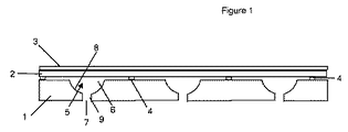
図1に示されるように、スピーカは、約3mmの厚さを有する第1の層又はバックプレーン1を備える。第1の層又はバックプレーン1は、上面に導電層(図示しない)を備えている絶縁ポリマーから構成されている。この層の上には、絶縁ポリマーフィルムの可撓性を有する層2があり、その上には、導電層3がある。導電層3及び絶縁層2は、別個の層とすることができるが、この実施形態においては、導電層3は、金属膜の形態で絶縁層2の外面に適用されて、約12ミクロンの総厚を有するフィルムが設けられているが、いくつかの実施形態においては約6ミクロンの厚さのフィルムが使用されてもよい。Myler(商標)からなる絶縁ストリップ4が層1及び2の間に配置されている。これらのストリップは、1から2mmの幅を有し、20から25ミクロンの厚さを有する。
As shown in FIG. 1, the speaker comprises a first layer or
バックプレーン1は、貫通開口5のアレイを備えている。貫通開口5のそれぞれは、絶縁層2に面した入口6と、出口7とを有する。各開口の上部8は、湾曲して凹面となっており、収束壁を提供する。この上部8はまた、バックプレーンの上面にある層と接続された導電層を備えている。開口の下部は、単純な平行側面を有する孔9の形態である。この実施形態において、開口入口は、12mmの直径を有する円形である。
The
図2からわかるように、絶縁ストリップは、開口5の間に設けられている。
図面は、正確な縮尺ではなく、関係する原理を説明するために変換器の一部のみが示されている。
As can be seen from FIG. 2, the insulating strip is provided between the
The drawings are not to scale and only a portion of the transducer is shown to illustrate the principles involved.
この実施形態にかかる1つの構成において、規則正しい円形開口のアレイがある。
図3を参照すると、およそ200から400ボルトのDCバイアス電圧がバックプレーン1の導電部と外層3との間に印加される。約200ボルトの交流信号はまた、バックプレーン1と外層3との間に印加される。その効果は、層2及び3を有するフィルムが静電力の結果としてバックプレーンに向かって、且つバックプレーンから離れて移動するというものである。開口5を覆う領域において、フィルム2/3は、膨らみ10を形成する。図示するように、フィルム2/3は、開口5の領域において、バックプレーン1に向かって突出しているが、フィルム2/3は、また、バックプレーンから離れる方向にも突出する。この実施形態において、フィルムに向かって突出するとき、膨らみ10は、開口5内に突出することができる。
In one configuration according to this embodiment, there is an array of regular circular apertures.
Referring to FIG. 3, a DC bias voltage of approximately 200 to 400 volts is applied between the conductive portion of the
図4の実施形態において、絶縁スペーサストリップ4が使用され、この場合、バックプレーンに向かって、且つバックプレーンから離れて突出する膨らみがフィルム2/3上に形成されるが、この実施形態においては、バックプレーンに向かって突出するとき、膨らみは、開口5内に突出しない。しかしながら、他の実施形態において、スペーサを使用しても、膨らみは、開口内に突出することがある。
In the embodiment of FIG. 4, an insulating spacer strip 4 is used, in which case a bulge is formed on the
図5の実施形態において、バックプレーン1は、変更された開口11を備えている。この開口11は、開口のより浅い収束部を提供する直線の収束壁12を有する。壁12は、導電性を有する。したがって、開口の出口に通じる下部13は、先の構成におけるものよりも長い。
In the embodiment of FIG. 5, the
図6は、本発明を組み込んだスピーカを示している。バックプレーン1は、この場合は金属化ポリマーフィルムの単一シートによって提供される絶縁及び導電層2/3によって覆われており、フレーム14は、開口を有するバックプレーンの全体に亘って比較的緊張してこれらの層を保持するために設けられている。全体アセンブリは、約3mm厚とすることができる。他の構成において、バックプレーンは、より可撓性を有していてもよく、組み立て品はより薄くなる。
FIG. 6 shows a speaker incorporating the present invention. The
図7は、比較的小さいサイズの開口17を有する内側領域16と、比較的大きいサイズの開口19を有する外側領域18とを備えた変更されたバックプレーン15を示している。このような構成により、2つの領域の周波数応答又は他の特性を異なるものとすることができ、一方の領域を他方よりも低い又は高い周波数により適したものとすることができる。
FIG. 7 shows a modified
図8は、バックプレーン1が変更された開口20を備えたさらなる実施形態を示している。変更された開口20は、内側に向けられた段差22において終端となっている直線の側壁21を有する上部を有する。下部23は、開口の出口に通じている。少なくとも段差22、望ましくは上部側壁21は、導電性を有する。
FIG. 8 shows a further embodiment in which the
図9は、図1の実施形態の変更例を示している。この変更された実施形態において、第1及び第2の層間の間隔ストリップ4は、横方向に間隔をあけて2つの層を一体に接合し、且つ層を離隔するのにも役立つ接着剤24からなるストリップに置き換えられている。さらにまた、結合した第2及び第3の層は、横方向に間隔をあけて2つの層を一体に接合し、且つ層を離隔するのにも役立つ接着剤27からなるストリップによって分離された別個の第2の層25及び第3の層26に置き換えられている。
FIG. 9 shows a modification of the embodiment of FIG. In this modified embodiment, the spacing strip 4 between the first and second layers is separated from the adhesive 24 which is laterally spaced to join the two layers together and also to separate the layers. Has been replaced by a strip. Furthermore, the joined second and third layers are separated by a strip of adhesive 27 that serves to join the two layers together in a laterally spaced manner and also to separate the layers. The second layer 25 and the
図10は、例えば図9の実施形態において使用される代わりの第1の層を示している。これは、単純な開口29のアレイを有するプレート28の形態である。プレート28は、金属製か、又は金属層によって被覆されているポリマーとすることができる。例えば電気メッキによって、開口が形成される前にコーティングが行われる場合、開口は、導電壁を有しない。しかしながら、層間にスペーサを有する実施形態においては、さらに先行技術に対して向上した性能がある。
FIG. 10 shows an alternative first layer used, for example, in the embodiment of FIG. This is in the form of a
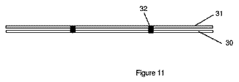
図11は、第2及び第3の層についてのさらに代わりの構成を示している。別個の第2の層30及び別個の第3の層31がある。これらは、例えば溶接によって、離隔された線32に沿って結合される。溶接線間において、層は離隔されている。
FIG. 11 shows a further alternative configuration for the second and third layers. There is a separate
本発明の望ましい実施形態は、音声性能が向上した小型で安価な薄型スピーカを提供する。 The preferred embodiment of the present invention provides a small and inexpensive thin speaker with improved audio performance.
Claims (15)
Applications Claiming Priority (3)
| Application Number | Priority Date | Filing Date | Title |
|---|---|---|---|
| GB1108373.0A GB2490931A (en) | 2011-05-19 | 2011-05-19 | Electrostatic acoustic transducer |
| GB1108373.0 | 2011-05-19 | ||
| PCT/GB2012/051130 WO2012156753A1 (en) | 2011-05-19 | 2012-05-18 | Electrostatic transducer |
Publications (3)
| Publication Number | Publication Date |
|---|---|
| JP2014517603A JP2014517603A (en) | 2014-07-17 |
| JP2014517603A5 JP2014517603A5 (en) | 2015-07-09 |
| JP6089029B2 true JP6089029B2 (en) | 2017-03-01 |
Family
ID=44260757
Family Applications (1)
| Application Number | Title | Priority Date | Filing Date |
|---|---|---|---|
| JP2014510886A Active JP6089029B2 (en) | 2011-05-19 | 2012-05-18 | Electrostatic transducer |
Country Status (6)
| Country | Link |
|---|---|
| US (1) | US9503821B2 (en) |
| EP (1) | EP2710815B1 (en) |
| JP (1) | JP6089029B2 (en) |
| CN (1) | CN103843369B (en) |
| GB (1) | GB2490931A (en) |
| WO (1) | WO2012156753A1 (en) |
Families Citing this family (9)
| Publication number | Priority date | Publication date | Assignee | Title |
|---|---|---|---|---|
| GB2522931A (en) * | 2014-02-11 | 2015-08-12 | Warwick Audio Technologies Ltd | Improved electrostatic transducer |
| GB2522932A (en) | 2014-02-11 | 2015-08-12 | Warwick Audio Technologies Ltd | Improved electrostatic transducer |
| WO2017053716A1 (en) * | 2015-09-24 | 2017-03-30 | Frank Joseph Pompei | Ultrasonic transducers |
| US9667173B1 (en) * | 2016-04-26 | 2017-05-30 | Turtle Beach Corporation | Electrostatic parametric transducer and related methods |
| US9986355B2 (en) * | 2016-06-14 | 2018-05-29 | Bose Corporation | Assembly aid for miniature transducer |
| CN106714055B (en) * | 2016-12-31 | 2019-04-19 | 苏州清听声学科技有限公司 | Back pole plate multichannel electrostatic transducer |
| US11328701B2 (en) | 2019-01-06 | 2022-05-10 | Holosonic Research Labs | Ultrasonic transducer with perforated baseplate |
| GB201906425D0 (en) | 2019-05-07 | 2019-06-19 | Warwick Acoustics Ltd | Electrostatic transducer and diaphragm |
| CN113411966B (en) * | 2021-05-11 | 2022-04-15 | 武汉市木邦电器有限公司 | Welding method based on metal wire |
Family Cites Families (33)
| Publication number | Priority date | Publication date | Assignee | Title |
|---|---|---|---|---|
| GB228176A (en) * | 1924-01-22 | 1926-07-22 | Ernst Hueter | Improvements in vibratory diaphragms |
| US2975243A (en) * | 1958-01-17 | 1961-03-14 | Philco Corp | Transducers |
| US3895193A (en) | 1968-04-29 | 1975-07-15 | Pond Chester C | Cross-over network and bias voltage supply for dynamic-electrostatic speaker system |
| JPS5121791B2 (en) * | 1972-08-04 | 1976-07-05 | ||
| JPS5419172B2 (en) * | 1973-07-23 | 1979-07-13 | ||
| US3935397A (en) | 1974-01-28 | 1976-01-27 | Electronic Industries, Inc. | Electrostatic loudspeaker element |
| US3992585A (en) | 1975-10-06 | 1976-11-16 | Koss Corporation | Self-energizing electrostatic loudspeaker system |
| US4533794A (en) * | 1983-05-23 | 1985-08-06 | Beveridge Harold N | Electrode for electrostatic transducer |
| JPS6046196A (en) * | 1984-06-12 | 1985-03-12 | Matsushita Electric Ind Co Ltd | Diaphragm for speaker |
| US5161128A (en) | 1990-11-30 | 1992-11-03 | Ultrasonic Arrays, Inc. | Capacitive transducer system and method |
| WO1993001691A1 (en) | 1991-07-11 | 1993-01-21 | Driver Michael L | Electrolytic loudspeaker assembly |
| JP3277498B2 (en) | 1992-10-24 | 2002-04-22 | ソニー株式会社 | Speaker device |
| DE4425901A1 (en) | 1994-07-21 | 1996-01-25 | Siemens Ag | Control amplifier for controlling a high-resistance low voltage source |
| US5973368A (en) | 1996-06-05 | 1999-10-26 | Pearce; Lawrence G. | Monolithic class D amplifier |
| JP4388603B2 (en) * | 1997-02-07 | 2009-12-24 | エス アール アイ・インターナショナル | Elastic dielectric polymer film acoustic wave actuator |
| US6044160A (en) * | 1998-01-13 | 2000-03-28 | American Technology Corporation | Resonant tuned, ultrasonic electrostatic emitter |
| US6628791B1 (en) | 1999-10-29 | 2003-09-30 | American Technology Corporation | Signal derived bias supply for electrostatic loudspeakers |
| US7095864B1 (en) | 2000-09-02 | 2006-08-22 | University Of Warwick | Electrostatic audio loudspeakers |
| US20020141606A1 (en) | 2001-02-09 | 2002-10-03 | Richard Schweder | Power supply assembly |
| GB2413027A (en) | 2004-04-01 | 2005-10-12 | Steve Kelsey | Bias for electrostatic loudspeaker is dependent upon signal level |
| US7595580B2 (en) * | 2005-03-21 | 2009-09-29 | Artificial Muscle, Inc. | Electroactive polymer actuated devices |
| JP4822517B2 (en) * | 2005-05-24 | 2011-11-24 | パナソニック株式会社 | Speaker device |
| JP4682927B2 (en) * | 2005-08-03 | 2011-05-11 | セイコーエプソン株式会社 | Electrostatic ultrasonic transducer, ultrasonic speaker, audio signal reproduction method, ultrasonic transducer electrode manufacturing method, ultrasonic transducer manufacturing method, superdirective acoustic system, and display device |
| JP4793174B2 (en) | 2005-11-25 | 2011-10-12 | セイコーエプソン株式会社 | Electrostatic transducer, circuit constant setting method |
| JP4867565B2 (en) | 2005-11-29 | 2012-02-01 | セイコーエプソン株式会社 | Capacitive load drive circuit and ultrasonic speaker |
| RU2440693C2 (en) | 2006-01-03 | 2012-01-20 | Транспарент Саунд Текнолоджи БИ.ВИ.,NL | Electrostatic acoustic systems and methods |
| GB0600014D0 (en) | 2006-01-03 | 2006-02-08 | Warwick Audio Technologies Ltd | Electrostatic loudspeakers |
| TW200908542A (en) | 2007-08-10 | 2009-02-16 | Richtek Technology Corp | Driving device for electrostatic loudspeaker |
| JP5262288B2 (en) * | 2007-09-27 | 2013-08-14 | ヤマハ株式会社 | Electrostatic speaker |
| JP5169208B2 (en) | 2007-12-21 | 2013-03-27 | ヤマハ株式会社 | Wireless speaker device |
| JP2009284397A (en) * | 2008-05-26 | 2009-12-03 | Yamaha Corp | Electrostatic speaker |
| TWI330501B (en) * | 2008-06-05 | 2010-09-11 | Ind Tech Res Inst | Flexible electret transducer assembly, speaker and method of making a flexible electret transducer assembly |
| JP2010004254A (en) * | 2008-06-19 | 2010-01-07 | Yamaha Corp | Electrostatic speaker |
-
2011
- 2011-05-19 GB GB1108373.0A patent/GB2490931A/en not_active Withdrawn
-
2012
- 2012-05-18 WO PCT/GB2012/051130 patent/WO2012156753A1/en active Application Filing
- 2012-05-18 US US14/118,761 patent/US9503821B2/en active Active
- 2012-05-18 EP EP12723735.2A patent/EP2710815B1/en active Active
- 2012-05-18 CN CN201280035607.2A patent/CN103843369B/en active Active
- 2012-05-18 JP JP2014510886A patent/JP6089029B2/en active Active
Also Published As
| Publication number | Publication date |
|---|---|
| US20140232236A1 (en) | 2014-08-21 |
| JP2014517603A (en) | 2014-07-17 |
| GB201108373D0 (en) | 2011-06-29 |
| CN103843369B (en) | 2018-03-30 |
| GB2490931A (en) | 2012-11-21 |
| WO2012156753A1 (en) | 2012-11-22 |
| CN103843369A (en) | 2014-06-04 |
| US9503821B2 (en) | 2016-11-22 |
| EP2710815A1 (en) | 2014-03-26 |
| EP2710815B1 (en) | 2016-10-19 |
Similar Documents
| Publication | Publication Date | Title |
|---|---|---|
| JP6089029B2 (en) | Electrostatic transducer | |
| JP6048469B2 (en) | Electroacoustic transducer | |
| JP4215788B2 (en) | Piezoelectric electroacoustic transducer | |
| JP4231879B2 (en) | Piezoelectric electroacoustic transducer | |
| JP6048470B2 (en) | Electroacoustic transducer | |
| US20200177996A1 (en) | Speaker | |
| CN106331961A (en) | Micro acoustic generator | |
| JP2015233272A (en) | Electroacoustic transducer | |
| JP2020039179A (en) | Improved electrostatic speaker | |
| WO2017053716A1 (en) | Ultrasonic transducers | |
| JP3395672B2 (en) | Piezoelectric electroacoustic transducer | |
| CN108513236B (en) | Loudspeaker vibrating structure and loudspeaker | |
| JP2004096225A (en) | Piezoelectric sound generating device | |
| CN106714055B (en) | Back pole plate multichannel electrostatic transducer | |
| JP6065819B2 (en) | Electroacoustic transducer | |
| JP2001119793A (en) | Piezoelectric speaker | |
| AU2006341771A1 (en) | An electrostatic loudspeaker | |
| JP2531026B2 (en) | Waterproof speaker | |
| JP6481480B2 (en) | Electroacoustic transducer | |
| CN1242922A (en) | Piezoelectric electro electroacoustic transducer | |
| JP6265539B2 (en) | Capacitor headphone unit and method of manufacturing capacitor headphone fixed pole assembly | |
| JP7099110B2 (en) | Electro-acoustic converter | |
| JP6187666B2 (en) | Electroacoustic transducer | |
| JP5760878B2 (en) | Electrostatic acoustic transducer | |
| JP6065820B2 (en) | Electroacoustic transducer |
Legal Events
| Date | Code | Title | Description |
|---|---|---|---|
| A521 | Request for written amendment filed |
Free format text: JAPANESE INTERMEDIATE CODE: A523 Effective date: 20150518 |
|
| A621 | Written request for application examination |
Free format text: JAPANESE INTERMEDIATE CODE: A621 Effective date: 20150518 |
|
| A131 | Notification of reasons for refusal |
Free format text: JAPANESE INTERMEDIATE CODE: A131 Effective date: 20160216 |
|
| A601 | Written request for extension of time |
Free format text: JAPANESE INTERMEDIATE CODE: A601 Effective date: 20160510 |
|
| A521 | Request for written amendment filed |
Free format text: JAPANESE INTERMEDIATE CODE: A523 Effective date: 20160808 |
|
| TRDD | Decision of grant or rejection written | ||
| A01 | Written decision to grant a patent or to grant a registration (utility model) |
Free format text: JAPANESE INTERMEDIATE CODE: A01 Effective date: 20170111 |
|
| A61 | First payment of annual fees (during grant procedure) |
Free format text: JAPANESE INTERMEDIATE CODE: A61 Effective date: 20170206 |
|
| R150 | Certificate of patent or registration of utility model |
Ref document number: 6089029 Country of ref document: JP Free format text: JAPANESE INTERMEDIATE CODE: R150 |
|
| S531 | Written request for registration of change of domicile |
Free format text: JAPANESE INTERMEDIATE CODE: R313531 |
|
| S533 | Written request for registration of change of name |
Free format text: JAPANESE INTERMEDIATE CODE: R313533 |
|
| R350 | Written notification of registration of transfer |
Free format text: JAPANESE INTERMEDIATE CODE: R350 |
|
| R250 | Receipt of annual fees |
Free format text: JAPANESE INTERMEDIATE CODE: R250 |
|
| R250 | Receipt of annual fees |
Free format text: JAPANESE INTERMEDIATE CODE: R250 |
|
| R250 | Receipt of annual fees |
Free format text: JAPANESE INTERMEDIATE CODE: R250 |
|
| R250 | Receipt of annual fees |
Free format text: JAPANESE INTERMEDIATE CODE: R250 |
|
| R250 | Receipt of annual fees |
Free format text: JAPANESE INTERMEDIATE CODE: R250 |