JP6074295B2 - Electrophotographic photosensitive member, process cartridge and electrophotographic apparatus, and method for manufacturing electrophotographic photosensitive member - Google Patents
Electrophotographic photosensitive member, process cartridge and electrophotographic apparatus, and method for manufacturing electrophotographic photosensitive member Download PDFInfo
- Publication number
- JP6074295B2 JP6074295B2 JP2013053506A JP2013053506A JP6074295B2 JP 6074295 B2 JP6074295 B2 JP 6074295B2 JP 2013053506 A JP2013053506 A JP 2013053506A JP 2013053506 A JP2013053506 A JP 2013053506A JP 6074295 B2 JP6074295 B2 JP 6074295B2
- Authority
- JP
- Japan
- Prior art keywords
- oxide particles
- conductive layer
- tin oxide
- particles
- photosensitive member
- Prior art date
- Legal status (The legal status is an assumption and is not a legal conclusion. Google has not performed a legal analysis and makes no representation as to the accuracy of the status listed.)
- Active
Links
Images


Classifications
-
- G—PHYSICS
- G03—PHOTOGRAPHY; CINEMATOGRAPHY; ANALOGOUS TECHNIQUES USING WAVES OTHER THAN OPTICAL WAVES; ELECTROGRAPHY; HOLOGRAPHY
- G03G—ELECTROGRAPHY; ELECTROPHOTOGRAPHY; MAGNETOGRAPHY
- G03G5/00—Recording members for original recording by exposure, e.g. to light, to heat, to electrons; Manufacture thereof; Selection of materials therefor
- G03G5/02—Charge-receiving layers
- G03G5/04—Photoconductive layers; Charge-generation layers or charge-transporting layers; Additives therefor; Binders therefor
- G03G5/043—Photoconductive layers characterised by having two or more layers or characterised by their composite structure
- G03G5/047—Photoconductive layers characterised by having two or more layers or characterised by their composite structure characterised by the charge-generation layers or charge transport layers
-
- G—PHYSICS
- G03—PHOTOGRAPHY; CINEMATOGRAPHY; ANALOGOUS TECHNIQUES USING WAVES OTHER THAN OPTICAL WAVES; ELECTROGRAPHY; HOLOGRAPHY
- G03G—ELECTROGRAPHY; ELECTROPHOTOGRAPHY; MAGNETOGRAPHY
- G03G5/00—Recording members for original recording by exposure, e.g. to light, to heat, to electrons; Manufacture thereof; Selection of materials therefor
- G03G5/02—Charge-receiving layers
- G03G5/04—Photoconductive layers; Charge-generation layers or charge-transporting layers; Additives therefor; Binders therefor
-
- G—PHYSICS
- G03—PHOTOGRAPHY; CINEMATOGRAPHY; ANALOGOUS TECHNIQUES USING WAVES OTHER THAN OPTICAL WAVES; ELECTROGRAPHY; HOLOGRAPHY
- G03G—ELECTROGRAPHY; ELECTROPHOTOGRAPHY; MAGNETOGRAPHY
- G03G15/00—Apparatus for electrographic processes using a charge pattern
- G03G15/06—Apparatus for electrographic processes using a charge pattern for developing
-
- G—PHYSICS
- G03—PHOTOGRAPHY; CINEMATOGRAPHY; ANALOGOUS TECHNIQUES USING WAVES OTHER THAN OPTICAL WAVES; ELECTROGRAPHY; HOLOGRAPHY
- G03G—ELECTROGRAPHY; ELECTROPHOTOGRAPHY; MAGNETOGRAPHY
- G03G5/00—Recording members for original recording by exposure, e.g. to light, to heat, to electrons; Manufacture thereof; Selection of materials therefor
- G03G5/10—Bases for charge-receiving or other layers
- G03G5/104—Bases for charge-receiving or other layers comprising inorganic material other than metals, e.g. salts, oxides, carbon
-
- G—PHYSICS
- G03—PHOTOGRAPHY; CINEMATOGRAPHY; ANALOGOUS TECHNIQUES USING WAVES OTHER THAN OPTICAL WAVES; ELECTROGRAPHY; HOLOGRAPHY
- G03G—ELECTROGRAPHY; ELECTROPHOTOGRAPHY; MAGNETOGRAPHY
- G03G5/00—Recording members for original recording by exposure, e.g. to light, to heat, to electrons; Manufacture thereof; Selection of materials therefor
- G03G5/14—Inert intermediate or cover layers for charge-receiving layers
- G03G5/142—Inert intermediate layers
- G03G5/144—Inert intermediate layers comprising inorganic material
Description
本発明は、電子写真感光体、電子写真感光体を有するプロセスカートリッジおよび電子写真装置、ならびに、電子写真感光体の製造方法に関する。 The present invention relates to an electrophotographic photosensitive member, a process cartridge and an electrophotographic apparatus having the electrophotographic photosensitive member, and a method for manufacturing the electrophotographic photosensitive member.
近年、有機光導電性材料を用いた電子写真感光体(有機電子写真感光体)の研究開発が盛んに行われている。 In recent years, research and development of electrophotographic photoreceptors (organic electrophotographic photoreceptors) using organic photoconductive materials have been actively conducted.
電子写真感光体は、基本的には、支持体と、該支持体上に形成された感光層とから構成される。しかしながら、現状は、支持体の表面の欠陥の隠蔽、感光層の電気的破壊に対する保護、帯電性の向上、支持体から感光層への電荷注入阻止性の改良などのために、支持体と感光層との間には、各種の層が設けられることが多い。 An electrophotographic photosensitive member basically includes a support and a photosensitive layer formed on the support. However, the present situation is that the support and photosensitive layer are exposed in order to conceal defects on the surface of the support, protect against electrical breakdown of the photosensitive layer, improve chargeability, and improve the charge injection prevention property from the support to the photosensitive layer. Various layers are often provided between the layers.
支持体と感光層との間に設けられる層の中でも、支持体の表面の欠陥の隠蔽を目的として設けられる層としては、金属酸化物粒子を含有する層が知られている。金属酸化物粒子を含有する層は、一般的に、金属酸化物粒子を含有しない層に比べて導電性が高く(例えば、体積抵抗率で1.0×10⁸〜5.0×10¹²Ω・cm)、層の膜厚を厚くしても、画像形成時の残留電位の上昇が生じにくい。そのため、支持体の表面の欠陥を隠蔽することが容易である。このような導電性の高い層(以下「導電層」という。)を支持体と感光層との間に設けて支持体の表面の欠陥を隠蔽することにより、支持体の表面の欠陥の許容範囲は大きくなる。その結果、支持体の使用許容範囲が大幅に広がるため、電子写真感光体の生産性の向上が図れるという利点がある。 Among the layers provided between the support and the photosensitive layer, a layer containing metal oxide particles is known as a layer provided for the purpose of concealing defects on the surface of the support. A layer containing metal oxide particles generally has higher conductivity than a layer not containing metal oxide particles (for example, 1.0 × 10 8 to 5.0 × 10 12 Ω in volume resistivity). (Cm), even if the layer thickness is increased, the residual potential is hardly increased during image formation. Therefore, it is easy to conceal defects on the surface of the support. By providing such a highly conductive layer (hereinafter referred to as “conductive layer”) between the support and the photosensitive layer to conceal defects on the surface of the support, the tolerance of defects on the surface of the support is allowed. Becomes bigger. As a result, since the allowable use range of the support is greatly expanded, there is an advantage that the productivity of the electrophotographic photosensitive member can be improved.
特許文献1には、支持体とバリア層、感光層との間の中間層にタンタルがドープされている酸化スズ粒子を用いる技術が記載されている。また、特許文献2および3には、支持体と感光層との間の導電層または中間層にニオブがドープされている酸化スズ粒子を用いる技術が記載されている。
Patent Document 1 describes a technique using tin oxide particles in which tantalum is doped in an intermediate layer between a support, a barrier layer, and a photosensitive layer.
しかしながら、本発明者らの検討の結果、上記のような金属酸化物粒子を含有する層を導電層として採用した電子写真感光体を用いて低温低湿環境下で繰り返して画像形成を行うと、電子写真感光体にリークが発生しやすくなることが判明した。リークとは、電子写真感光体の局所部分で絶縁破壊が発生し、その部分に過剰な電流が流れる現象のことである。リークが発生すると、電子写真感光体を十分に帯電することができず、黒点、横黒スジなどの画像不良につながる。横黒スジとは、電子写真感光体の回転方向(周方向)に直交する方向の黒いスジである。 However, as a result of the study by the present inventors, when an image is formed repeatedly in a low-temperature and low-humidity environment using an electrophotographic photosensitive member that employs a layer containing metal oxide particles as described above as a conductive layer, It has been found that leaks are likely to occur in the photographic photoreceptor. Leakage is a phenomenon in which dielectric breakdown occurs in a local portion of the electrophotographic photosensitive member, and an excessive current flows through that portion. When leakage occurs, the electrophotographic photosensitive member cannot be sufficiently charged, leading to image defects such as black spots and horizontal black stripes. The horizontal black stripe is a black stripe in a direction orthogonal to the rotation direction (circumferential direction) of the electrophotographic photosensitive member.
本発明の目的は、金属酸化物粒子を含有する層を導電層として採用した電子写真感光体であっても、リークが発生しにくい電子写真感光体、該電子写真感光体を有するプロセスカートリッジおよび電子写真装置、ならびに、該電子写真感光体を製造する方法を提供することにある。 An object of the present invention is to provide an electrophotographic photosensitive member in which leakage hardly occurs even when an electrophotographic photosensitive member adopting a layer containing metal oxide particles as a conductive layer, a process cartridge having the electrophotographic photosensitive member, and an electronic It is an object to provide a photographic apparatus and a method for producing the electrophotographic photosensitive member.
本発明は、円筒状支持体と、導電層と、感光層と、をこの順に有する電子写真感光体において、
該導電層が、
(1)ニオブがドープされている酸化スズで被覆されている酸化チタン粒子、
(2)タンタルがドープされている酸化スズで被覆されている酸化チタン粒子、
(3)ニオブがドープされている酸化スズで被覆されている酸化スズ粒子、
(4)タンタルがドープされている酸化スズで被覆されている酸化スズ粒子、
(5)ニオブがドープされている酸化スズで被覆されている酸化亜鉛粒子、および
(6)タンタルがドープされている酸化スズで被覆されている酸化亜鉛粒子
からなる群から選択される少なくとも1種の金属酸化物粒子と、
結着材料と、を含有し、
該導電層の体積抵抗率が、1.0×10 8 Ω・cm以上5.0×10 12 Ω・cm以下であり、
該円筒状支持体と該導電層とから構成される試験用サンプルに対し、常温常湿(23℃/50%RH)環境下において、定電圧−1.0kVの直流電圧(直流成分のみ)を、
{(I t −I t+1 )/I t }×100
(電圧印加からt[分]後における電流量の絶対値をI t [μA]とし、t+1[分]後における電流量の絶対値をI t+1 [μA]とする)
が初めて1%以下になるまで連続して印加する試験を行った場合に、
該I t+1 が10μA以上となり、
該試験における最大電流量の絶対値(Ia)が6000μA以下となることを特徴とする電子写真感光体である。
The present invention includes a cylindrical support, a conductive layer, an electrophotographic photosensitive member comprising a sensitive optical layer, in this order,
The conductive layer is
(1) Titanium oxide particles coated with tin oxide doped with niobium,
(2) Titanium oxide particles coated with tin oxide doped with tantalum,
(3) Tin oxide particles coated with tin oxide doped with niobium,
(4) Tin oxide particles coated with tin oxide doped with tantalum,
(5) zinc oxide particles coated with tin oxide doped with niobium, and
(6) Zinc oxide particles coated with tin oxide doped with tantalum
At least one metal oxide particle selected from the group consisting of:
Containing a binder material, a
The volume resistivity of the conductive layer is 1.0 × 10 8 Ω · cm to 5.0 × 10 12 Ω · cm,
A DC voltage (DC component only) of a constant voltage of −1.0 kV is applied to a test sample composed of the cylindrical support and the conductive layer in a normal temperature and normal humidity (23 ° C./50% RH) environment. ,
{(I t −I t + 1 ) / I t } × 100
(The absolute value of the current amount after t [minute] from the voltage application is I t [μA], and the absolute value of the current amount after t + 1 [minute] is I t + 1 [μA].)
When the test is continuously applied until the value becomes 1% or less for the first time,
The It + 1 becomes 10 μA or more,
The electrophotographic photosensitive member is characterized in that the absolute value (Ia) of the maximum current amount in the test is 6000 μA or less .
また、本発明は、上記電子写真感光体と、帯電手段、現像手段、転写手段およびクリーニング手段からなる群より選択される少なくとも1つの手段とを一体に支持し、電子写真装置本体に着脱自在であることを特徴とするプロセスカートリッジである。 Further, the present invention integrally supports the electrophotographic photosensitive member and at least one means selected from the group consisting of a charging means, a developing means, a transfer means, and a cleaning means, and is detachable from the main body of the electrophotographic apparatus. It is a process cartridge characterized by being.
また、本発明は、上記電子写真感光体、ならびに、帯電手段、露光手段、現像手段および転写手段を有することを特徴とする電子写真装置である。 The present invention also provides an electrophotographic apparatus comprising the above-described electrophotographic photosensitive member, and a charging unit, an exposing unit, a developing unit, and a transfer unit.
また、本発明は、円筒状支持体と、導電層と、感光層と、をこの順に有する電子写真感光体の製造方法であって、
該導電層が、溶剤、結着材料、および、(1)〜(6)からなる群から選択される少なくとも1種の金属酸化物粒子を含有する導電層用塗布液を調製し、該円筒状支持体に塗布することで形成され、
該金属酸化物粒子の粉体抵抗率が、1.0×10³Ω・cm以上1.0×10⁵Ω・cm以下であり、
該導電層用塗布液における、該金属酸化物粒子(P)と結着材料(B)の質量比(P/B)が、1.5/1.0以上3.5/1.0以下であり、
該導電層の体積抵抗率が、1.0×10 8 Ω・cm以上5.0×10 12 Ω・cm以下であることを特徴とする電子写真感光体の製造方法である。
(1)ニオブがドープされている酸化スズで被覆されている酸化チタン粒子
(2)タンタルがドープされている酸化スズで被覆されている酸化チタン粒子
(3)ニオブがドープされている酸化スズで被覆されている酸化スズ粒子
(4)タンタルがドープされている酸化スズで被覆されている酸化スズ粒子
(5)ニオブがドープされている酸化スズで被覆されている酸化亜鉛粒子
(6)タンタルがドープされている酸化スズで被覆されている酸化亜鉛粒子
Further, the present invention is a method for producing an electrophotographic photosensitive member having a cylindrical support, a conductive layer, and a photosensitive layer in this order ,
Conductive layer, a solvent, a binder material, and, (1) to a conductive layer coating liquid containing at least one metal oxide particles are selected from the group consisting of (6) was prepared, the cylindrical Formed by coating on a support,
Powder resistivity of the metal oxide particles is not more than 1.0 × 10 3 Ω · cm or more 1.0 × 10 5 Ω · cm,
In the conductive layer coating liquid, the weight ratio of the metal oxide particles (P) and binder material (B) (P / B) is 1.5 / 1.0 to 3.5 / 1.0 or less Oh it is,
A volume resistivity of the conductive layer is 1.0 × 10 8 Ω · cm or more and 5.0 × 10 12 Ω · cm or less .
(1) Titanium oxide particles coated with tin oxide doped with niobium
(2) Titanium oxide particles coated with tin oxide doped with tantalum
(3) Tin oxide particles coated with tin oxide doped with niobium
(4) Tin oxide particles coated with tin oxide doped with tantalum
(5) Zinc oxide particles coated with tin oxide doped with niobium
(6) Zinc oxide particles coated with tin oxide doped with tantalum
本発明によれば、金属酸化物粒子を含有する層を導電層として採用した電子写真感光体であっても、リークが発生しにくい電子写真感光体、該電子写真感光体を有するプロセスカートリッジおよび電子写真装置、ならびに、該電子写真感光体を製造する方法を提供することができる。 According to the present invention, even in an electrophotographic photosensitive member that employs a layer containing metal oxide particles as a conductive layer, an electrophotographic photosensitive member that does not easily leak, a process cartridge having the electrophotographic photosensitive member, and an electronic A photographic apparatus and a method for producing the electrophotographic photosensitive member can be provided.
本発明の電子写真感光体は、円筒状支持体(以下単に「支持体」ともいう。)、該円筒状支持体上に形成された導電層、および、該導電層上に形成された感光層を有する電子写真感光体である。 The electrophotographic photosensitive member of the present invention includes a cylindrical support (hereinafter also simply referred to as “support”), a conductive layer formed on the cylindrical support, and a photosensitive layer formed on the conductive layer. An electrophotographic photosensitive member having
感光層は、電荷発生物質および電荷輸送物質を単一の層に含有させた単層型感光層であってもよいし、電荷発生物質を含有する電荷発生層と電荷輸送物質を含有する電荷輸送層とを積層した積層型感光層であってもよい。また、必要に応じて、導電層と感光層との間に下引き層(中間層またはバリア層とも呼ばれる。)を設けてもよい。 The photosensitive layer may be a single layer type photosensitive layer containing a charge generation material and a charge transport material in a single layer, or a charge generation layer containing a charge generation material and a charge transport containing a charge transport material. It may be a laminated photosensitive layer in which layers are laminated. If necessary, an undercoat layer (also referred to as an intermediate layer or a barrier layer) may be provided between the conductive layer and the photosensitive layer.
支持体としては、導電性を有するもの(導電性支持体)が好ましく、例えば、アルミニウム、アルミニウム合金、ステンレス鋼などの金属で形成されている金属製支持体を用いることができる。アルミニウムやアルミニウム合金を用いる場合は、押し出し工程および引き抜き工程を含む製造方法により製造されるアルミニウム管や、押し出し工程およびしごき工程を含む製造方法により製造されるアルミニウム管を用いることができる。このようなアルミニウム管は、表面を切削することなく良好な寸法精度や表面平滑性が得られるうえ、コスト的にも有利である。しかしながら、無切削のアルミニウム管の表面にはササクレ状の凸状欠陥が生じやすいため、導電層を設けることが特に有効である。 As the support, those having conductivity (conductive support) are preferable, and for example, a metal support formed of a metal such as aluminum, an aluminum alloy, or stainless steel can be used. In the case of using aluminum or an aluminum alloy, an aluminum tube manufactured by a manufacturing method including an extrusion process and a drawing process, or an aluminum pipe manufactured by a manufacturing method including an extrusion process and an ironing process can be used. Such an aluminum tube is advantageous in terms of cost as well as obtaining good dimensional accuracy and surface smoothness without cutting the surface. However, it is particularly effective to provide a conductive layer because the surface of the non-cut aluminum tube is likely to have a crusted convex defect.
本発明においては、支持体の表面の欠陥の隠蔽を目的として、支持体上には、体積抵抗率が1.0×10⁸Ω・cm以上5.0×10¹²Ω・cm以下の導電層が設けられる。なお、この導電層の体積抵抗率は、後述の直流電圧連続印加試験を行う場合、直流電圧連続印加試験の前に測定された体積抵抗率を意味する。支持体の表面の欠陥を隠蔽するための層として、体積抵抗率が5.0×10¹²Ω・cmを超える層を支持体上に設けると、画像形成時に電荷の流れが滞りやすくなり、残留電位が上昇しやすくなる。一方、導電層の体積抵抗率が1.0×10⁸Ω・cm未満であると、導電層中を流れる電荷の量が多くなりすぎて、リークが発生しやすくなる。 In the present invention, for the purpose of concealing defects on the surface of the support, a conductive layer having a volume resistivity of 1.0 × 10 8 Ω · cm to 5.0 × 10 12 Ω · cm is formed on the support. Is provided. The volume resistivity of the conductive layer means the volume resistivity measured before the DC voltage continuous application test when a DC voltage continuous application test described later is performed. If a layer having a volume resistivity of more than 5.0 × 10 12 Ω · cm is provided on the support as a layer for concealing defects on the surface of the support, the flow of charges tends to stagnate at the time of image formation. The potential tends to rise. On the other hand, if the volume resistivity of the conductive layer is less than 1.0 × 10 8 Ω · cm, the amount of charge flowing in the conductive layer becomes too large, and leakage tends to occur.
図2および図3を用いて、電子写真感光体の導電層の体積抵抗率を測定する方法を説明する。図2は、導電層の体積抵抗率の測定方法を説明するための上面図であり、図3は、導電層の体積抵抗率の測定方法を説明するための断面図である。 A method for measuring the volume resistivity of the conductive layer of the electrophotographic photosensitive member will be described with reference to FIGS. FIG. 2 is a top view for explaining a method for measuring the volume resistivity of the conductive layer, and FIG. 3 is a cross-sectional view for explaining the method for measuring the volume resistivity of the conductive layer.
導電層の体積抵抗率は、常温常湿(23℃/50%RH)環境下において測定する。導電層202の表面に銅製テープ203(住友スリーエム(株)製、型番No.1181)を貼り、これを導電層202の表面側の電極とする。また、支持体201を導電層202の裏面側の電極とする。銅製テープ203と支持体201との間に電圧を印加するための電源206、および、銅製テープ203と支持体201との間を流れる電流を測定するための電流測定機器207をそれぞれ設置する。また、銅製テープ203に電圧を印加するため、銅製テープ203の上に銅線204を載せ、銅線204が銅製テープ203からはみ出さないように銅線204の上から銅製テープ203と同様の銅製テープ205を貼り、銅製テープ203に銅線204を固定する。銅製テープ203には、銅線204を用いて電圧を印加する。
The volume resistivity of the conductive layer is measured under a normal temperature and normal humidity (23 ° C./50% RH) environment. A copper tape 203 (manufactured by Sumitomo 3M Co., Ltd., model number No. 1181) is attached to the surface of the
銅製テープ203と支持体201との間に電圧を印加しないときのバックグラウンド電流値をI0[A]とし、直流電圧(直流成分)のみの電圧を−1V印加したときの電流値をI[A]とし、導電層202の膜厚d[cm]、導電層202の表面側の電極(銅製テープ203)の面積をS[cm2]とするとき、下記数式(1)で表される値を導電層202の体積抵抗率ρ[Ω・cm]とする。
ρ=1/(I−I0)×S/d[Ω・cm] ・・・(1)
この測定では、絶対値で1×10⁻⁶A以下という微小な電流量を測定する。そのため、電流測定機器207としては、微小電流の測定が可能な機器を用いて行うことが好ましい。そのような機器としては、例えば、横河ヒューレットパッカード社製のpAメーター(商品名:4140B)などが挙げられる。
The background current value when no voltage is applied between the
ρ = 1 / (I−I 0 ) × S / d [Ω · cm] (1)
In this measurement, a minute current amount of 1 × 10 −6 A or less in absolute value is measured. Therefore, it is preferable that the
なお、導電層の体積抵抗率は、支持体上に導電層のみを形成した状態で測定しても、電子写真感光体から導電層上の各層(感光層など)を剥離して支持体上に導電層のみを残した状態で測定しても、同様の値を示す。 Even if the volume resistivity of the conductive layer is measured in a state where only the conductive layer is formed on the support, each layer (such as the photosensitive layer) on the conductive layer is peeled off from the electrophotographic photosensitive member on the support. Even when the measurement is performed with only the conductive layer left, the same value is obtained.
本発明において、導電層は、溶剤、結着材料、および、ニオブまたはタンタルがドープされている酸化スズで被覆されている金属酸化物粒子を用いて調製された導電層用塗布液を用いて形成することができる。すなわち、本発明においては、導電層用の金属酸化物粒子として、ニオブまたはタンタルがドープされている酸化スズで被覆されている金属酸化物粒子が用いられる。ニオブまたはタンタルがドープされている酸化スズで被覆されている金属酸化物粒子を、以下「Nb/Taドープ酸化スズ被覆金属酸化物粒子」ともいう。本発明で用いられるNb/Taドープ酸化スズ被覆金属酸化物粒子は、金属酸化物で構成されている芯材粒子と、ニオブまたはタンタルがドープされている酸化スズで構成されている被覆層とを有しており、該被覆層が該芯材粒子を被覆している構造になっている。このような被覆層が芯材粒子を被覆している構造になっている粒子は、複合粒子とも呼ばれる。 In the present invention, the conductive layer is formed using a solvent, a binder material, and a conductive layer coating solution prepared using metal oxide particles coated with tin oxide doped with niobium or tantalum. can do. That is, in the present invention, metal oxide particles coated with tin oxide doped with niobium or tantalum are used as the metal oxide particles for the conductive layer. Hereinafter, the metal oxide particles coated with tin oxide doped with niobium or tantalum are also referred to as “Nb / Ta-doped tin oxide-coated metal oxide particles”. The Nb / Ta-doped tin oxide-coated metal oxide particles used in the present invention comprise a core particle composed of a metal oxide and a coating layer composed of tin oxide doped with niobium or tantalum. And has a structure in which the coating layer coats the core particles. The particles having such a structure that the coating layer covers the core particles are also called composite particles.
芯材粒子を構成する金属酸化物としては、被覆層を構成している酸化スズと同じ酸化スズである場合と、酸化スズ以外の金属酸化物である場合とに大別される。芯材粒子を構成する金属酸化物のうち、酸化スズ以外の金属酸化物としては、例えば、酸化チタン、酸化ジルコニウム、酸化亜鉛などが挙げられ、これらの中でも、酸化チタン、酸化亜鉛が好適に用いられる。また、芯材粒子を構成する金属酸化物は、ノンドープの金属酸化物であることが好ましい。芯材粒子を構成する金属酸化物が酸化スズであって、かつ、該酸化スズがノンドープである場合、被覆層はニオブまたはタンタルがドープされている部分であり、芯材粒子はニオブやタンタルなどのドーパントがドープされていない部分であり、両者を容易に区別することができる。 The metal oxide constituting the core particle is roughly classified into a case where it is the same tin oxide as the tin oxide constituting the coating layer and a case where it is a metal oxide other than tin oxide. Among the metal oxides constituting the core particles, examples of metal oxides other than tin oxide include titanium oxide, zirconium oxide, and zinc oxide. Among these, titanium oxide and zinc oxide are preferably used. It is done. The metal oxide constituting the core particle is preferably a non-doped metal oxide. When the metal oxide constituting the core particle is tin oxide and the tin oxide is non-doped, the coating layer is a portion doped with niobium or tantalum, and the core particle is niobium or tantalum This is a portion where the dopant is not doped, and both can be easily distinguished.
また、本発明で用いられるNb/Taドープ酸化スズ被覆金属酸化物粒子(複合粒子)は、その粒子(複合粒子)の表面側の60質量%の領域に、その粒子にドープされているドーパント(ニオブ、タンタル)の90〜100質量%が存在していることが好ましく、100質量%が存在していることがより好ましい。 Further, the Nb / Ta-doped tin oxide-coated metal oxide particles (composite particles) used in the present invention are doped with dopants (60% by mass on the surface side of the particles (composite particles)). Niobium, tantalum) is preferably present in an amount of 90 to 100% by mass, more preferably 100% by mass.
導電層用塗布液は、Nb/Taドープ酸化スズ被覆金属酸化物粒子を結着材料とともに溶剤に分散させることによって調製することができる。分散方法としては、例えば、ペイントシェーカー、サンドミル、ボールミル、液衝突型高速分散機を用いた方法が挙げられる。導電層は、上記のように調製された導電層用塗布液を支持体上に塗布し、これを乾燥および/または硬化させることによって形成することができる。 The coating liquid for the conductive layer can be prepared by dispersing Nb / Ta-doped tin oxide-coated metal oxide particles in a solvent together with a binder material. Examples of the dispersion method include a method using a paint shaker, a sand mill, a ball mill, and a liquid collision type high-speed disperser. The conductive layer can be formed by applying the conductive layer coating solution prepared as described above onto a support, and drying and / or curing it.
また、耐リーク性の向上および残留電位上昇の抑制の観点から、導電層に直流電圧(直流成分)のみの電圧−1.0kVを連続印加する試験(「直流電圧連続印加試験」ともいう。)を行った場合の導電層を流れる最大電流量の絶対値をIa[μA]とし、導電層を流れる1分あたりの電流量の減少率が初めて1%以下になったときの導電層を流れる電流量の絶対値をIb[μA]としたとき、IaおよびIbが、下記関係式(i)および(ii)を満足することが好ましい。直流電圧連続印加試験の詳細については、後述する。
Ia≦6000 ・・・(i)
10≦Ib ・・・(ii)
In addition, from the viewpoint of improving leakage resistance and suppressing increase in residual potential, a test in which a voltage of only DC voltage (DC component) −1.0 kV is continuously applied to the conductive layer (also referred to as “DC voltage continuous application test”). The absolute value of the maximum amount of current flowing through the conductive layer in the case of performing Ia is set to Ia [μA], and the current flowing through the conductive layer when the rate of decrease in the amount of current per minute flowing through the conductive layer becomes 1% or less for the first time When the absolute value of the quantity is Ib [μA], it is preferable that Ia and Ib satisfy the following relational expressions (i) and (ii). Details of the DC voltage continuous application test will be described later.
Ia ≦ 6000 (i)
10 ≦ Ib (ii)
以下、上記最大電流量の絶対値であるIaを「最大電流量Ia」ともいい、上記電流量の絶対値であるIbを「電流量Ib」ともいう。 Hereinafter, Ia that is the absolute value of the maximum current amount is also referred to as “maximum current amount Ia”, and Ib that is the absolute value of the current amount is also referred to as “current amount Ib”.
導電層を流れる最大電流量Iaが6000μAを超えると、電子写真感光体の耐リーク性が低下しやすくなる。最大電流量Iaが6000μAを超える導電層は、局所的に過剰に電流が流れやすく、リークを引き起こす絶縁破壊が生じやすいと考えられる。耐リーク性をより向上させるには、最大電流量Iaは5000μA以下(Ia≦5000 ・・・(iii))であることが好ましい。 When the maximum current amount Ia flowing through the conductive layer exceeds 6000 μA, the leakage resistance of the electrophotographic photosensitive member tends to be lowered. It is considered that the conductive layer having the maximum current amount Ia exceeding 6000 μA tends to cause an excessive current to flow locally and easily cause a dielectric breakdown that causes a leak. In order to further improve the leakage resistance, the maximum current amount Ia is preferably 5000 μA or less (Ia ≦ 5000 (iii)).
一方、導電層を流れる電流量Ibが10μA未満であると、画像形成時の電子写真感光体の残留電位が上昇しやすくなる。電流量Ibが10μA未満の導電層は、残留電位の上昇を引き起こす電荷の流れの滞りが生じやすいと考えられる。残留電位の上昇をより抑えるには、電流量Ibは20μA以上(20≦Ib ・・・(iv))であることが好ましい。 On the other hand, if the amount of current Ib flowing through the conductive layer is less than 10 μA, the residual potential of the electrophotographic photosensitive member during image formation tends to increase. It is considered that the conductive layer having a current amount Ib of less than 10 μA is likely to cause a charge flow stagnation that causes an increase in residual potential. In order to further suppress the increase in the residual potential, the current amount Ib is preferably 20 μA or more (20 ≦ Ib (iv)).
また、耐リーク性の向上の観点から、あるいは、最大電流量Iaを6000μA以下にする観点から、導電層に用いられるNb/Taドープ酸化スズ被覆金属酸化物粒子の粉体抵抗率は、1.0×103Ω・cm以上であることが好ましい。 From the viewpoint of improving leakage resistance, or from the viewpoint of reducing the maximum current Ia to 6000 μA or less, the powder resistivity of the Nb / Ta-doped tin oxide-coated metal oxide particles used for the conductive layer is 1. It is preferably 0 × 10 3 Ω · cm or more.
Nb/Taドープ酸化スズ被覆金属酸化物粒子の粉体抵抗率が1.0×103Ω・cm未満であると、電子写真感光体の耐リーク性が低下しやすくなる。これは、Nb/Taドープ酸化スズ被覆金属酸化物粒子の粉体抵抗率に応じて、Nb/Taドープ酸化スズ被覆金属酸化物粒子によって形成される導電層中の導電パスの状態が異なるためであると考えられる。Nb/Taドープ酸化スズ被覆金属酸化物粒子の粉体抵抗率が1.0×103Ω・cm未満である場合、Nb/Taドープ酸化スズ被覆金属酸化物粒子の個々を流れる電荷の量は多くなりやすい。一方、Nb/Taドープ酸化スズ被覆金属酸化物粒子の粉体抵抗率が1.0×103Ω・cm以上である場合、Nb/Taドープ酸化スズ被覆金属酸化物粒子の個々を流れる電荷の量は少なくなりやすい。具体的にいえば、粉体抵抗率が1.0×103Ω・cm未満のNb/Taドープ酸化スズ被覆金属酸化物粒子を用いて形成された導電層であっても、粉体抵抗率が1.0×103Ω・cm以上のNb/Taドープ酸化スズ被覆金属酸化物粒子を用いて形成された導電層であっても、両者(導電層)の体積抵抗率が同じである場合は、両者を流れるトータルの電荷の量は同じであると考えられる。導電層を流れるトータルの電荷の量が同じであれば、粉体抵抗率が1.0×103Ω・cm未満のNb/Taドープ酸化スズ被覆金属酸化物粒子と、粉体抵抗率が1.0×103Ω・cm以上のNb/Taドープ酸化スズ被覆金属酸化物粒子とでは、Nb/Taドープ酸化スズ被覆金属酸化物粒子の個々に流れる電荷の量が異なることになる。 When the powder resistivity of the Nb / Ta-doped tin oxide-coated metal oxide particles is less than 1.0 × 10 3 Ω · cm, the leakage resistance of the electrophotographic photosensitive member tends to be lowered. This is because the state of the conductive path in the conductive layer formed by the Nb / Ta-doped tin oxide-coated metal oxide particles varies depending on the powder resistivity of the Nb / Ta-doped tin oxide-coated metal oxide particles. It is believed that there is. When the powder resistivity of the Nb / Ta-doped tin oxide coated metal oxide particles is less than 1.0 × 10 3 Ω · cm, the amount of charge flowing through each of the Nb / Ta-doped tin oxide coated metal oxide particles is It tends to increase. On the other hand, when the powder resistivity of the Nb / Ta-doped tin oxide-coated metal oxide particles is 1.0 × 10 3 Ω · cm or more, the charge flowing through each of the Nb / Ta-doped tin oxide-coated metal oxide particles is reduced. The amount tends to decrease. Specifically, even if the conductive layer is formed using Nb / Ta-doped tin oxide-coated metal oxide particles having a powder resistivity of less than 1.0 × 10 3 Ω · cm, the powder resistivity Is the conductive layer formed using Nb / Ta-doped tin oxide-coated metal oxide particles of 1.0 × 10 3 Ω · cm or more, but the volume resistivity of both (conductive layer) is the same Is considered to have the same total charge flowing through both. If the total amount of charge flowing through the conductive layer is the same, the powder resistivity is less than 1.0 × 10 3 Ω · cm, Nb / Ta-doped tin oxide coated metal oxide particles, and the powder resistivity is 1 The amount of charge flowing individually in the Nb / Ta-doped tin oxide-coated metal oxide particles is different from that of Nb / Ta-doped tin oxide-coated metal oxide particles of 0.0 × 10 3 Ω · cm or more.
このことは、粉体抵抗率が1.0×10³Ω・cm未満のNb/Taドープ酸化スズ被覆金属酸化物粒子を用いて形成された導電層と、粉体抵抗率が1.0×103Ω・cm以上のNb/Taドープ酸化スズ被覆金属酸化物粒子を用いて形成された導電層とでは、導電層中の導電パスの数が異なることを意味する。具体的には、粉体抵抗率が1.0×103Ω・cm以上のNb/Taドープ酸化スズ被覆金属酸化物粒子を用いて形成された導電層の方が、粉体抵抗率が1.0×103Ω・cm未満のNb/Taドープ酸化スズ被覆金属酸化物粒子を用いて形成された導電層に比べて、導電層中の導電パスの数が多いと推測される。 This is because a conductive layer formed using Nb / Ta-doped tin oxide coated metal oxide particles having a powder resistivity of less than 1.0 × 10 3 Ω · cm, and a powder resistivity of 1.0 × This means that the number of conductive paths in the conductive layer is different from that of the conductive layer formed using Nb / Ta-doped tin oxide-coated metal oxide particles of 10 3 Ω · cm or more. Specifically, a conductive layer formed using Nb / Ta-doped tin oxide-coated metal oxide particles having a powder resistivity of 1.0 × 10 3 Ω · cm or more has a powder resistivity of 1 It is estimated that the number of conductive paths in the conductive layer is larger than that of the conductive layer formed using Nb / Ta-doped tin oxide-coated metal oxide particles of less than 0.0 × 10 3 Ω · cm.
したがって、粉体抵抗率が1.0×10³Ω・cm以上のNb/Taドープ酸化スズ被覆金属酸化物粒子を用いて導電層を形成した場合、導電層中の導電パス1本あたりを流れる電荷の量が比較的少なくなり、各導電パスにおいて局所的に過剰な電流が流れることが抑制されることになり、電子写真感光体の耐リーク性の向上につながっていると考えられる。耐リーク性をより向上させるには、導電層に用いられるNb/Taドープ酸化スズ被覆金属酸化物粒子の粉体抵抗率は、3.0×103Ω・cm以上であることが好ましい。 Therefore, when a conductive layer is formed using Nb / Ta-doped tin oxide-coated metal oxide particles having a powder resistivity of 1.0 × 10 3 Ω · cm or more, it flows around one conductive path in the conductive layer. It is considered that the amount of charge is relatively small, and an excessive current is locally prevented from flowing in each conductive path, leading to an improvement in leakage resistance of the electrophotographic photosensitive member. In order to further improve the leak resistance, the powder resistivity of the Nb / Ta-doped tin oxide-coated metal oxide particles used for the conductive layer is preferably 3.0 × 10 3 Ω · cm or more.
また、残留電位上昇の抑制の観点から、あるいは、電流量Ibを10μA以上にする観点から、導電層に用いられるNb/Taドープ酸化スズ被覆金属酸化物粒子の粉体抵抗率は、1.0×105Ω・cm以下であることが好ましい。 From the viewpoint of suppressing the increase in residual potential, or from the viewpoint of setting the current amount Ib to 10 μA or more, the powder resistivity of the Nb / Ta-doped tin oxide-coated metal oxide particles used for the conductive layer is 1.0. It is preferable that it is x10 < 5 > ohm * cm or less.
Nb/Taドープ酸化スズ被覆金属酸化物粒子の粉体抵抗率が1.0×105Ω・cmを超えると、画像形成時に電子写真感光体の残留電位が上昇しやすくなる。また、導電層の体積抵抗率を5.0×1012Ω・cm以下に調整しにくくなる。残留電位上昇をより抑制するには、導電層に用いられるNb/Taドープ酸化スズ被覆金属酸化物粒子の粉体抵抗率は、5.0×104Ω・cm以下であることが好ましい。 If the powder resistivity of the Nb / Ta-doped tin oxide-coated metal oxide particles exceeds 1.0 × 10 5 Ω · cm, the residual potential of the electrophotographic photosensitive member tends to increase during image formation. Moreover, it becomes difficult to adjust the volume resistivity of the conductive layer to 5.0 × 10 12 Ω · cm or less. In order to further suppress the increase in residual potential, the powder resistivity of the Nb / Ta-doped tin oxide-coated metal oxide particles used for the conductive layer is preferably 5.0 × 10 4 Ω · cm or less.
以上の理由より、導電層に用いられるNb/Taドープ酸化スズ被覆金属酸化物粒子の粉体抵抗率は、1.0×103Ω・cm以上1.0×105Ω・cm以下であることが好ましく、3.0×103Ω・cm以上5.0×104Ω・cm以下であることがより好ましい。 For the above reasons, the powder resistivity of the Nb / Ta-doped tin oxide-coated metal oxide particles used for the conductive layer is 1.0 × 10 3 Ω · cm or more and 1.0 × 10 5 Ω · cm or less. It is preferably 3.0 × 10 3 Ω · cm or more and 5.0 × 10 4 Ω · cm or less.
Nb/Taドープ酸化スズ被覆金属酸化物粒子は、酸素欠損型の酸化スズ(SnO2)で被覆されている酸化チタン(TiO2)粒子(以下「酸素欠損型酸化スズ被覆酸化チタン粒子」ともいう。)よりも、電子写真感光体の耐リーク性を向上させる効果が大きく、また、画像形成時の残留電位の上昇を抑える効果も大きい。耐リーク性を向上させる効果が大きい理由については、金属酸化物粒子としてNb/Taドープ酸化スズ被覆金属酸化物粒子を用いた導電層は、酸素欠損型酸化スズ被覆酸化チタン粒子を用いた導電層に比べて、最大電流量Iaが小さく、耐圧性が高いためと考えられる。また、画像形成時の残留電位の上昇を抑える効果が大きい理由については、酸素欠損型酸化スズ被覆酸化チタン粒子は、酸素存在下で酸化して酸化スズ(SnO2)中の酸素欠損部位が消失し、粒子の抵抗が高くなり、導電層における電荷の流れが滞りやすくなるのに対して、Nb/Taドープ酸化スズ被覆金属酸化物粒子では、そのようなことが生じにくいためと考えられる。 The Nb / Ta-doped tin oxide-coated metal oxide particles are also referred to as titanium oxide (TiO 2 ) particles coated with oxygen-deficient tin oxide (SnO 2 ) (hereinafter also referred to as “oxygen-deficient tin oxide-coated titanium oxide particles”). The effect of improving the leakage resistance of the electrophotographic photosensitive member is greater than that of.), And the effect of suppressing the increase in residual potential during image formation is also greater. The reason why the effect of improving the leak resistance is great is that the conductive layer using Nb / Ta-doped tin oxide-coated metal oxide particles as the metal oxide particles is the conductive layer using oxygen-deficient tin oxide-coated titanium oxide particles. It is considered that the maximum current amount Ia is small and the pressure resistance is high. The reason why the effect of suppressing the increase in residual potential during image formation is large is that oxygen-deficient tin oxide-coated titanium oxide particles are oxidized in the presence of oxygen and the oxygen-deficient site in tin oxide (SnO 2 ) disappears. However, the resistance of the particles becomes high and the flow of electric charges in the conductive layer tends to be stagnant, whereas such a phenomenon is unlikely to occur in Nb / Ta-doped tin oxide-coated metal oxide particles.
Nb/Taドープ酸化スズ被覆金属酸化物粒子における酸化スズ(SnO2)の割合(被覆率)は、10〜60質量%であることが好ましい。酸化スズ(SnO2)の被覆率を制御するためには、Nb/Taドープ酸化スズ被覆金属酸化物粒子を製造するときに、酸化スズ(SnO2)を生成するのに必要なスズ原材料を配合する必要がある。例えば、スズ原材料として塩化スズ(SnCl4)を用いる場合、塩化スズ(SnCl4)から生成される酸化スズ(SnO2)の量を考慮した仕込みである必要がある。なお、この場合の被覆率は、酸化スズ(SnO2)にドープされているニオブまたはタンタルの質量を考慮に入れず、被覆層を構成する酸化スズ(SnO2)と芯材粒子を構成する金属酸化物(酸化チタン、酸化ジルコニウム、酸化亜鉛、酸化スズなど。)の合計質量に対する、被覆層を構成する酸化スズ(SnO2)の質量により計算した値とする。酸化スズ(SnO2)の被覆率が10質量%より小さい場合、Nb/Taドープ酸化スズ被覆金属酸化物粒子の粉体抵抗率を1.0×105Ω・cm以下に調整しにくくなる。被覆率が60質量%より大きい場合、酸化スズ(SnO2)による芯材粒子の被覆が不均一になりやすく、また、高コストになりやすく、また、Nb/Taドープ酸化スズ被覆金属酸化物粒子の粉体抵抗率を1.0×103Ω・cm以上に調整しにくい。 The ratio (coverage) of tin oxide (SnO 2 ) in the Nb / Ta-doped tin oxide-coated metal oxide particles is preferably 10 to 60% by mass. In order to control the coverage of the tin oxide (SnO 2), when producing with Nb / Ta-doped tin oxide coated metal oxide particles, blending the tin raw material necessary to produce a tin oxide (SnO 2) There is a need to. For example, when tin chloride (SnCl 4 ) is used as a tin raw material, the preparation needs to take into account the amount of tin oxide (SnO 2 ) produced from tin chloride (SnCl 4 ). The metal the coverage of cases, without taking into account the mass of niobium or tantalum doped in tin oxide (SnO 2), which constitutes a tin oxide (SnO 2) and the core particles constituting the coating layer A value calculated by the mass of tin oxide (SnO 2 ) constituting the coating layer with respect to the total mass of oxide (titanium oxide, zirconium oxide, zinc oxide, tin oxide, etc.). When the coverage of tin oxide (SnO 2 ) is smaller than 10% by mass, it becomes difficult to adjust the powder resistivity of the Nb / Ta-doped tin oxide-coated metal oxide particles to 1.0 × 10 5 Ω · cm or less. When the coverage is larger than 60% by mass, the coating of the core material particles with tin oxide (SnO 2 ) is likely to be non-uniform and expensive, and the Nb / Ta-doped tin oxide coated metal oxide particles It is difficult to adjust the powder resistivity to 1.0 × 10 3 Ω · cm or more.
また、酸化スズ(SnO2)にドープされるニオブまたはタンタルの量は、酸化スズ(SnO2)(ニオブまたはタンタルを含まない質量)に対して0.1〜10質量%であることが好ましい。酸化スズ(SnO2)にドープされるニオブまたはタンタルの量が0.1質量%より少ない場合、Nb/Taドープ酸化スズ被覆金属酸化物粒子の粉体抵抗率を1.0×105Ω・cm以下に調整しにくくなる。酸化スズ(SnO2)にドープされるニオブまたはタンタルの量が10質量%より多い場合、酸化スズ(SnO2)の結晶性が低下し、Nb/Taドープ酸化スズ被覆金属酸化物粒子の粉体抵抗率を1.0×103Ω・cm以上(1.0×105Ω・cm以下)に調整しにくくなる。一般的には、酸化スズ(SnO2)にニオブまたはタンタルをドープすることにより、ドープしていないものに比べて、粒子の粉体抵抗率を低くすることができる。 The amount of niobium or tantalum is doped tin oxide (SnO 2) is preferably 0.1 to 10 mass% with respect to tin oxide (SnO 2) (mass containing no niobium or tantalum). When the amount of niobium or tantalum doped in tin oxide (SnO 2 ) is less than 0.1% by mass, the powder resistivity of the Nb / Ta-doped tin oxide-coated metal oxide particles is 1.0 × 10 5 Ω · It becomes difficult to adjust to below cm. When the amount of niobium or tantalum doped in tin oxide (SnO 2 ) is more than 10% by mass, the crystallinity of tin oxide (SnO 2 ) decreases, and the powder of Nb / Ta-doped tin oxide coated metal oxide particles It becomes difficult to adjust the resistivity to 1.0 × 10 3 Ω · cm or more (1.0 × 10 5 Ω · cm or less). In general, by doping niobium or tantalum into tin oxide (SnO 2 ), the powder resistivity of the particles can be lowered as compared with those not doped.
なお、ニオブまたはタンタルがドープされている酸化スズ(SnO2)で被覆されている酸化チタン粒子の製造方法は、特開2004−349167号公報に開示されている。また、酸化スズ(SnO2)で被覆されている酸化スズ粒子の製造方法は、特開2010−030886号公報に開示されている。 Incidentally, a method for producing titanium oxide particles coated with tin oxide (SnO 2 ) doped with niobium or tantalum is disclosed in Japanese Patent Application Laid-Open No. 2004-349167. The manufacturing method of the tin oxide particles coated with tin oxide (SnO 2) is disclosed in JP-A-2010-030886.
本発明において、Nb/Taドープ酸化スズ被覆金属酸化物粒子などの金属酸化物粒子の粉体抵抗率の測定方法は以下のとおりである。 In the present invention, the method for measuring the powder resistivity of metal oxide particles such as Nb / Ta-doped tin oxide-coated metal oxide particles is as follows.
金属酸化物粒子の粉体抵抗率は、常温常湿(23℃/50%RH)環境下において測定する。本発明においては、測定装置として、三菱化学(株)製の抵抗率計(商品名:ロレスタGP)を用いた。測定対象の金属酸化物粒子は、500kg/cm2の圧力で固めて、ペレット状の測定用サンプルにする。印加電圧は100Vとする。 The powder resistivity of the metal oxide particles is measured under a normal temperature and normal humidity (23 ° C./50% RH) environment. In the present invention, a resistivity meter (trade name: Loresta GP) manufactured by Mitsubishi Chemical Corporation was used as a measuring device. The metal oxide particles to be measured are hardened at a pressure of 500 kg / cm 2 to form a pellet-shaped measurement sample. The applied voltage is 100V.
本発明において、導電層に、金属酸化物で構成されている芯材粒子を有する粒子(Nb/Taドープ酸化スズ被覆金属酸化物粒子)を用いるのは、導電層用塗布液における金属酸化物粒子の分散性の向上を図るためである。ニオブまたはタンタルがドープされている酸化スズ(SnO2)のみからなる粒子を用いた場合、導電層用塗布液における金属酸化物粒子の粒径が大きくなりやすく、導電層の表面に凸状のブツ欠陥が発生し、耐リーク性が低下したり、導電層用塗布液の安定性が低下したりする場合がある。 In the present invention, particles having core material particles composed of metal oxide (Nb / Ta-doped tin oxide-coated metal oxide particles) are used for the conductive layer in the conductive layer. This is to improve the dispersibility of the resin. When particles made of only tin oxide (SnO 2 ) doped with niobium or tantalum are used, the particle size of the metal oxide particles in the coating liquid for the conductive layer tends to be large, and the surface of the conductive layer has convex protrusions. Defects may occur, resulting in a decrease in leakage resistance and a decrease in the stability of the conductive layer coating solution.
また、芯材粒子を構成する材料として、酸化チタン(TiO2)、酸化ジルコニウム(ZrO2)、酸化スズ(SnO2)、酸化亜鉛(ZnO)などの金属酸化物を用いるのは、耐リーク性を向上させやすいからである。さらに、粒子としての透明性が低く、支持体の表面の欠陥を隠蔽しやすいからである。これに対して、芯材粒子を構成する材料として、例えば、金属酸化物ではない硫酸バリウムを用いた場合、導電層中を流れる電荷の量が多くなりやすく、耐リーク性を向上させにくい。また、粒子としての透明性が高いために、支持体の表面の欠陥を隠蔽するための材料が別途必要になる場合がある。 In addition, the use of metal oxides such as titanium oxide (TiO 2 ), zirconium oxide (ZrO 2 ), tin oxide (SnO 2 ), and zinc oxide (ZnO) as the material constituting the core material particles is resistant to leakage. It is because it is easy to improve. Furthermore, it is because the transparency as particles is low and it is easy to conceal defects on the surface of the support. On the other hand, when, for example, barium sulfate that is not a metal oxide is used as the material constituting the core material particles, the amount of charge flowing in the conductive layer is likely to increase, and it is difficult to improve the leak resistance. Moreover, since the transparency as particles is high, a material for concealing defects on the surface of the support may be required separately.
また、金属酸化物粒子として、非被覆の金属酸化物粒子ではなく、ニオブまたはタンタルがドープされている酸化スズ(SnO2)で被覆されている金属酸化物粒子を用いるのは、非被覆の金属酸化物粒子では、画像形成時に電荷の流れが滞りやすくなり、残留電位が上昇しやすくなるからである。 Further, as the metal oxide particles, metal oxide particles coated with tin oxide (SnO 2 ) doped with niobium or tantalum are used instead of uncoated metal oxide particles. This is because the oxide particles tend to stagnate the charge flow during image formation, and the residual potential tends to increase.
導電層用塗布液の調製に用いられる結着材料としては、例えば、フェノール樹脂、ポリウレタン、ポリアミド、ポリイミド、ポリアミドイミド、ポリビニルアセタール、エポキシ樹脂、アクリル樹脂、メラミン樹脂、ポリエステルなどの樹脂が挙げられる。これらは1種または2種以上用いることができる。また、これらの樹脂の中でも、他層へのマイグレーション(溶け込み)の抑制、支持体への密着性、Nb/Taドープ酸化スズ被覆金属酸化物粒子の分散性・分散安定性、層形成後の耐溶剤性などの観点から、硬化性樹脂が好ましく、さらに、熱硬化性樹脂がより好ましい。また、熱硬化性樹脂の中でも、熱硬化性のフェノール樹脂、熱硬化性のポリウレタンが好ましい。導電層の結着材料として硬化性樹脂を用いる場合、導電層用塗布液に含有させる結着材料は、該硬化性樹脂のモノマーおよび/またはオリゴマーとなる。 Examples of the binder material used for preparing the coating liquid for the conductive layer include resins such as phenol resin, polyurethane, polyamide, polyimide, polyamideimide, polyvinyl acetal, epoxy resin, acrylic resin, melamine resin, and polyester. These can be used alone or in combination of two or more. Among these resins, the migration (melting) to other layers is suppressed, the adhesion to the support, the dispersibility / dispersion stability of the Nb / Ta-doped tin oxide-coated metal oxide particles, and the resistance after forming the layer. From the viewpoint of solvent properties, a curable resin is preferable, and a thermosetting resin is more preferable. Of the thermosetting resins, thermosetting phenol resins and thermosetting polyurethanes are preferred. When a curable resin is used as the binder material for the conductive layer, the binder material contained in the conductive layer coating solution is a monomer and / or oligomer of the curable resin.
導電層用塗布液に用いられる溶剤としては、例えば、メタノール、エタノール、イソプロパノールなどのアルコールや、アセトン、メチルエチルケトン、シクロへキサノンなどのケトンや、テトラヒドロフラン、ジオキサン、エチレングリコールモノメチルエーテル、プロピレングリコールモノメチルエーテルなどのエーテルや、酢酸メチル、酢酸エチルなどのエステルや、トルエン、キシレンなどの芳香族炭化水素が挙げられる。 Examples of the solvent used in the conductive layer coating solution include alcohols such as methanol, ethanol, isopropanol, ketones such as acetone, methyl ethyl ketone, and cyclohexanone, tetrahydrofuran, dioxane, ethylene glycol monomethyl ether, propylene glycol monomethyl ether, and the like. Ethers, esters such as methyl acetate and ethyl acetate, and aromatic hydrocarbons such as toluene and xylene.
また、本発明において、導電層用塗布液におけるNb/Taドープ酸化スズ被覆金属酸化物粒子(P)と結着材料(B)の質量比(P/B)は、1.5/1.0以上3.5/1.0以下であることが好ましい。質量比(P/B)が1.5/1.0未満である場合、画像形成時に電荷の流れが滞りやすくなり、残留電位が上昇しやすくなる。また、導電層の体積抵抗率を5.0×1012Ω・cm以下に調整しにくくなる。質量比(P/B)が3.5/1.0を超える場合、導電層の体積抵抗率を1.0×108Ω・cm以上に調整しにくくなり、また、Nb/Taドープ酸化スズ被覆金属酸化物粒子の結着が難しくなり、導電層にクラックが発生しやすくなり、耐リーク性を向上させにくい。 In the present invention, the mass ratio (P / B) of the Nb / Ta-doped tin oxide-coated metal oxide particles (P) and the binder material (B) in the conductive layer coating solution is 1.5 / 1.0. It is preferable that it is above 3.5 / 1.0. When the mass ratio (P / B) is less than 1.5 / 1.0, the flow of charges tends to stagnate during image formation, and the residual potential tends to increase. Moreover, it becomes difficult to adjust the volume resistivity of the conductive layer to 5.0 × 10 12 Ω · cm or less. When the mass ratio (P / B) exceeds 3.5 / 1.0, it becomes difficult to adjust the volume resistivity of the conductive layer to 1.0 × 10 8 Ω · cm or more, and Nb / Ta-doped tin oxide Binding of the coated metal oxide particles becomes difficult, cracks are likely to occur in the conductive layer, and leakage resistance is difficult to improve.
導電層の膜厚は、支持体の表面の欠陥を隠蔽するという観点から、10μm以上40μm以下であることが好ましく、15μm以上35μm以下であることがより好ましい。
なお、本発明においては、導電層を含む電子写真感光体の各層の膜厚の測定装置として、(株)フィッシャーインストルメンツ製のFISCHERSCOPE MMSを用いた。
The film thickness of the conductive layer is preferably 10 μm or more and 40 μm or less, more preferably 15 μm or more and 35 μm or less from the viewpoint of concealing defects on the surface of the support.
In the present invention, a FISCHERSCOPE MMS manufactured by Fisher Instruments Co., Ltd. was used as a film thickness measuring device for each layer of the electrophotographic photosensitive member including the conductive layer.
また、導電層用塗布液におけるNb/Taドープ酸化スズ被覆金属酸化物粒子の平均粒径は、0.10μm以上0.45μm以下であることが好ましく、0.15μm以上0.40μm以下であることがより好ましい。平均粒径が0.10μmより小さい場合、導電層用塗布液の調製後にNb/Taドープ酸化スズ被覆金属酸化物粒子の再凝集が起こり、導電層用塗布液の安定性が低下したり、導電層の表面にクラックが発生したりすることがある。平均粒径が0.45μmより大きい場合は、導電層の表面が荒れて、感光層への局所的な電荷注入が起こりやすくなり、出力画像の白地における黒ポチが目立つようになることがある。 The average particle size of the Nb / Ta-doped tin oxide-coated metal oxide particles in the conductive layer coating solution is preferably 0.10 μm or more and 0.45 μm or less, and preferably 0.15 μm or more and 0.40 μm or less. Is more preferable. When the average particle size is smaller than 0.10 μm, re-aggregation of the Nb / Ta-doped tin oxide-coated metal oxide particles occurs after the preparation of the coating solution for the conductive layer, and the stability of the coating solution for the conductive layer is reduced. Cracks may occur on the surface of the layer. When the average particle diameter is larger than 0.45 μm, the surface of the conductive layer becomes rough, local charge injection into the photosensitive layer is likely to occur, and black spots on the white background of the output image may become noticeable.
導電層用塗布液におけるNb/Taドープ酸化スズ被覆金属酸化物粒子などの金属酸化物粒子の平均粒径の測定は、以下のとおり、液相沈降法によって行うことができる。 The average particle diameter of metal oxide particles such as Nb / Ta-doped tin oxide-coated metal oxide particles in the conductive layer coating solution can be measured by a liquid phase precipitation method as follows.
まず、導電層用塗布液を、その調製に用いた溶剤で透過率が0.8〜1.0の間になるように希釈する。次に、超遠心式自動粒度分布測定装置を用いて、金属酸化物粒子の平均粒径(体積標準D50)および粒度分布のヒストグラムを作成する。本発明においては、超遠心式自動粒度分布測定装置として、(株)堀場製作所製の超遠心式自動粒度分布測定装置(商品名:CAPA700)を用い、回転数3000rpmの条件で測定を行った。 First, the conductive layer coating solution is diluted with the solvent used for the preparation so that the transmittance is between 0.8 and 1.0. Next, using an ultracentrifugal automatic particle size distribution measuring device, an average particle size (volume standard D50) of the metal oxide particles and a histogram of the particle size distribution are created. In the present invention, an ultracentrifugal automatic particle size distribution measuring apparatus (trade name: CAPA700) manufactured by Horiba, Ltd. was used as an ultracentrifugal automatic particle size distribution measuring apparatus, and measurement was performed under the condition of a rotational speed of 3000 rpm.
また、導電層の表面で反射した光が干渉して出力画像に干渉縞が発生することを抑制するため、導電層用塗布液には、導電層の表面を粗面化するための表面粗し付与材を含有させてもよい。表面粗し付与材としては、平均粒径が1μm以上5μm以下の樹脂粒子が好ましい。樹脂粒子としては、例えば、硬化性ゴム、ポリウレタン、エポキシ樹脂、アルキド樹脂、フェノール樹脂、ポリエステル、シリコーン樹脂、アクリル−メラミン樹脂などの硬化性樹脂の粒子が挙げられる。これらの中でも、凝集しにくいシリコーン樹脂の粒子が好ましい。樹脂粒子の比重(0.5〜2)は、Nb/Taドープ酸化スズ被覆金属酸化物粒子の比重(4〜7)に比べて小さいため、導電層形成時に効率的に導電層の表面を粗面化することができる。ただし、導電層中の表面粗し付与材の含有量が多いほど、導電層の体積抵抗率が上昇する傾向にあるため、導電層の体積抵抗率を5.0×1012Ω・cm以下に調整するためには、導電層用塗布液における表面粗し付与材の含有量は、導電層用塗布液中の結着材料に対して1〜80質量%であることが好ましい。 In order to suppress interference of light reflected on the surface of the conductive layer and generation of interference fringes in the output image, the coating liquid for the conductive layer has a surface roughening for roughening the surface of the conductive layer. An imparting material may be included. As the surface roughening material, resin particles having an average particle diameter of 1 μm or more and 5 μm or less are preferable. Examples of the resin particles include curable resin particles such as curable rubber, polyurethane, epoxy resin, alkyd resin, phenol resin, polyester, silicone resin, and acrylic-melamine resin. Among these, silicone resin particles that are difficult to aggregate are preferable. Since the specific gravity (0.5-2) of the resin particles is smaller than the specific gravity (4-7) of the Nb / Ta-doped tin oxide-coated metal oxide particles, the surface of the conductive layer is efficiently roughened when the conductive layer is formed. Can be surfaced. However, since the volume resistivity of the conductive layer tends to increase as the content of the surface roughening agent in the conductive layer increases, the volume resistivity of the conductive layer is set to 5.0 × 10 12 Ω · cm or less. In order to adjust, the content of the surface roughening agent in the conductive layer coating solution is preferably 1 to 80% by mass with respect to the binder material in the conductive layer coating solution.
また、導電層用塗布液には、導電層の表面性を高めるためのレベリング剤を含有させてもよい。また、導電層用塗布液には、導電層の隠蔽性を向上させるための顔料粒子を含有させてもよい。 The conductive layer coating solution may contain a leveling agent for enhancing the surface properties of the conductive layer. Moreover, you may make the coating liquid for conductive layers contain the pigment particle for improving the concealment property of a conductive layer.
導電層と感光層との間には、導電層から感光層への電荷注入を阻止するために、電気的バリア性を有する下引き層(バリア層)を設けてもよい。 An undercoat layer (barrier layer) having an electrical barrier property may be provided between the conductive layer and the photosensitive layer in order to prevent charge injection from the conductive layer to the photosensitive layer.
下引き層は、樹脂(結着樹脂)を含有する下引き層用塗布液を導電層上に塗布し、これを乾燥させることによって形成することができる。 The undercoat layer can be formed by applying an undercoat layer coating solution containing a resin (binder resin) on the conductive layer and drying it.
下引き層に用いられる樹脂(結着樹脂)としては、例えば、ポリビニルアルコール、ポリビニルメチルエーテル、ポリアクリル酸類、メチルセルロース、エチルセルロース、ポリグルタミン酸、カゼイン、でんぷんなどの水溶性樹脂や、ポリアミド、ポリイミド、ポリアミドイミド、ポリアミド酸、メラミン樹脂、エポキシ樹脂、ポリウレタン、ポリグルタミン酸エステルなどが挙げられる。これらの中でも、下引き層の電気的バリア性を効果的に発現させるためには、熱可塑性樹脂が好ましい。熱可塑性樹脂の中でも、熱可塑性のポリアミドが好ましい。ポリアミドとしては、共重合ナイロンが好ましい。 Examples of the resin (binder resin) used for the undercoat layer include water-soluble resins such as polyvinyl alcohol, polyvinyl methyl ether, polyacrylic acids, methyl cellulose, ethyl cellulose, polyglutamic acid, casein, and starch, polyamide, polyimide, and polyamide. Examples include imide, polyamic acid, melamine resin, epoxy resin, polyurethane, and polyglutamic acid ester. Among these, a thermoplastic resin is preferable in order to effectively develop the electrical barrier property of the undercoat layer. Of the thermoplastic resins, thermoplastic polyamide is preferable. As the polyamide, copolymer nylon is preferable.
下引き層の膜厚は、0.1μm以上2μm以下であることが好ましい。 The thickness of the undercoat layer is preferably from 0.1 μm to 2 μm.
また、下引き層において電荷の流れが滞らないようにするために、下引き層には、電子輸送物質(アクセプターなどの電子受容性物質)を含有させてもよい。電子輸送物質としては、例えば、2,4,7−トリニトロフルオレノン、2,4,5,7−テトラニトロフルオレノン、クロラニル、テトラシアノキノジメタンなどの電子吸引性物質や、これらの電子吸引性物質を高分子化したものなども挙げられる。 Further, in order to prevent the flow of electric charges in the undercoat layer, the undercoat layer may contain an electron transport material (electron accepting material such as an acceptor). Examples of electron transport materials include electron-withdrawing materials such as 2,4,7-trinitrofluorenone, 2,4,5,7-tetranitrofluorenone, chloranil, tetracyanoquinodimethane, and their electron-withdrawing materials. Examples include those obtained by polymerizing substances.
導電層または下引き層上には、感光層が設けられる。 A photosensitive layer is provided on the conductive layer or the undercoat layer.
感光層に用いられる電荷発生物質としては、例えば、モノアゾ、ジスアゾ、トリスアゾなどのアゾ顔料や、金属フタロシアニン、非金属フタロシアニンなどのフタロシアニン顔料や、インジゴ、チオインジゴなどのインジゴ顔料や、ペリレン酸無水物、ペリレン酸イミドなどのペリレン顔料や、アンスラキノン、ピレンキノンなどの多環キノン顔料や、スクワリリウム色素や、ピリリウム塩およびチアピリリウム塩や、トリフェニルメタン色素や、キナクリドン顔料や、アズレニウム塩顔料や、シアニン染料や、キサンテン色素や、キノンイミン色素や、スチリル色素などが挙げられる。これらの中でも、オキシチタニウムフタロシアニン、ヒドロキシガリウムフタロシアニン、クロロガリウムフタロシアニンなどの金属フタロシアニンが好ましい。 Examples of the charge generating material used in the photosensitive layer include azo pigments such as monoazo, disazo, and trisazo, phthalocyanine pigments such as metal phthalocyanine and nonmetal phthalocyanine, indigo pigments such as indigo and thioindigo, perylene acid anhydride, Perylene pigments such as perylene imide, polycyclic quinone pigments such as anthraquinone and pyrenequinone, squarylium dyes, pyrylium and thiapyrylium salts, triphenylmethane dyes, quinacridone pigments, azulenium salt pigments, cyanine dyes, Xanthene dyes, quinoneimine dyes, styryl dyes, and the like. Among these, metal phthalocyanines such as oxytitanium phthalocyanine, hydroxygallium phthalocyanine, and chlorogallium phthalocyanine are preferable.
感光層が積層型の感光層である場合、電荷発生層は、電荷発生物質を結着樹脂とともに溶剤に分散させることによって得られる電荷発生層用塗布液を塗布し、これを乾燥させることによって形成することができる。分散方法としては、例えば、ホモジナイザー、超音波、ボールミル、サンドミル、アトライター、ロールミルなどを用いた方法が挙げられる。 When the photosensitive layer is a laminated photosensitive layer, the charge generation layer is formed by applying a charge generation layer coating solution obtained by dispersing a charge generation material in a solvent together with a binder resin, and drying the coating solution. can do. Examples of the dispersion method include a method using a homogenizer, an ultrasonic wave, a ball mill, a sand mill, an attritor, a roll mill, and the like.
電荷発生層に用いられる結着樹脂としては、例えば、ポリカーボネート、ポリエステル、ポリアリレート、ブチラール樹脂、ポリスチレン、ポリビニルアセタール、ジアリルフタレート樹脂、アクリル樹脂、メタクリル樹脂、酢酸ビニル樹脂、フェノール樹脂、シリコーン樹脂、ポリスルホン、スチレン−ブタジエン共重合体、アルキッド樹脂、エポキシ樹脂、尿素樹脂、塩化ビニル−酢酸ビニル共重合体などが挙げられる。これらは、単独、混合または共重合体として1種または2種以上用いることができる。 Examples of the binder resin used for the charge generation layer include polycarbonate, polyester, polyarylate, butyral resin, polystyrene, polyvinyl acetal, diallyl phthalate resin, acrylic resin, methacrylic resin, vinyl acetate resin, phenol resin, silicone resin, polysulfone. Styrene-butadiene copolymer, alkyd resin, epoxy resin, urea resin, vinyl chloride-vinyl acetate copolymer, and the like. These may be used alone or in combination as a mixture or copolymer.
電荷発生物質と結着樹脂との割合(電荷発生物質:結着樹脂)は、10:1〜1:10(質量比)の範囲が好ましく、5:1〜1:1(質量比)の範囲がより好ましい。 The ratio of the charge generation material to the binder resin (charge generation material: binder resin) is preferably in the range of 10: 1 to 1:10 (mass ratio), and in the range of 5: 1 to 1: 1 (mass ratio). Is more preferable.
電荷発生層用塗布液に用いられる溶剤としては、例えば、アルコール、スルホキシド、ケトン、エーテル、エステル、脂肪族ハロゲン化炭化水素、芳香族化合物などが挙げられる。 Examples of the solvent used in the charge generation layer coating solution include alcohols, sulfoxides, ketones, ethers, esters, aliphatic halogenated hydrocarbons, and aromatic compounds.
電荷発生層の膜厚は、5μm以下であることが好ましく、0.1μm以上2μm以下であることがより好ましい。 The thickness of the charge generation layer is preferably 5 μm or less, and more preferably 0.1 μm or more and 2 μm or less.
また、電荷発生層には、種々の増感剤、酸化防止剤、紫外線吸収剤、可塑剤などを必要に応じて添加することもできる。また、電荷発生層において電荷の流れが滞らないようにするために、電荷発生層には、電子輸送物質(アクセプターなどの電子受容性物質)を含有させてもよい。電子輸送物質としては、例えば、2,4,7−トリニトロフルオレノン、2,4,5,7−テトラニトロフルオレノン、クロラニル、テトラシアノキノジメタンなどの電子吸引性物質や、これらの電子吸引性物質を高分子化したものなども挙げられる。 In addition, various sensitizers, antioxidants, ultraviolet absorbers, plasticizers, and the like can be added to the charge generation layer as necessary. In addition, in order to prevent the flow of charges from stagnation in the charge generation layer, the charge generation layer may contain an electron transport material (an electron accepting material such as an acceptor). Examples of electron transport materials include electron-withdrawing materials such as 2,4,7-trinitrofluorenone, 2,4,5,7-tetranitrofluorenone, chloranil, tetracyanoquinodimethane, and their electron-withdrawing materials. Examples include those obtained by polymerizing substances.
感光層に用いられる電荷輸送物質としては、例えば、トリアリールアミン化合物、ヒドラゾン化合物、スチリル化合物、スチルベン化合物、ピラゾリン化合物、オキサゾール化合物、チアゾール化合物、トリアリルメタン化合物などが挙げられる。 Examples of the charge transport material used in the photosensitive layer include triarylamine compounds, hydrazone compounds, styryl compounds, stilbene compounds, pyrazoline compounds, oxazole compounds, thiazole compounds, triallylmethane compounds, and the like.
感光層が積層型の感光層である場合、電荷輸送層は、電荷輸送物質および結着樹脂を溶剤に溶解させることによって得られる電荷輸送層用塗布液を塗布し、これを乾燥させることによって形成することができる。 When the photosensitive layer is a laminated type photosensitive layer, the charge transport layer is formed by applying a charge transport layer coating solution obtained by dissolving a charge transport material and a binder resin in a solvent, and drying it. can do.
電荷輸送層に用いられる結着樹脂としては、例えば、アクリル樹脂、スチレン樹脂、ポリエステル、ポリカーボネート、ポリアリレート、ポリサルホン、ポリフェニレンオキシド、エポキシ樹脂、ポリウレタン、アルキド樹脂、不飽和樹脂などが挙げられる。これらは、単独、混合物または共重合体として1種または2種以上用いることができる。 Examples of the binder resin used for the charge transport layer include acrylic resin, styrene resin, polyester, polycarbonate, polyarylate, polysulfone, polyphenylene oxide, epoxy resin, polyurethane, alkyd resin, and unsaturated resin. These can be used alone or in combination as a mixture or copolymer.
電荷輸送物質と結着樹脂との割合(電荷輸送物質:結着樹脂)は、2:1〜1:2(質量比)の範囲が好ましい。 The ratio of the charge transport material to the binder resin (charge transport material: binder resin) is preferably in the range of 2: 1 to 1: 2 (mass ratio).
電荷輸送層用塗布液に用いられる溶剤としては、例えば、アセトン、メチルエチルケトンなどのケトンや、酢酸メチル、酢酸エチルなどのエステルや、ジメトキシメタン、ジメトキシエタンなどのエーテルや、トルエン、キシレンなどの芳香族炭化水素や、クロロベンゼン、クロロホルム、四塩化炭素などのハロゲン原子で置換された炭化水素などが挙げられる。 Examples of the solvent used in the charge transport layer coating solution include ketones such as acetone and methyl ethyl ketone, esters such as methyl acetate and ethyl acetate, ethers such as dimethoxymethane and dimethoxyethane, and aromatics such as toluene and xylene. Examples include hydrocarbons and hydrocarbons substituted with halogen atoms such as chlorobenzene, chloroform and carbon tetrachloride.
電荷輸送層の膜厚は、帯電均一性や画像再現性の観点から、3μm以上40μm以下であることが好ましく、4μm以上30μm以下であることがより好ましい。 The thickness of the charge transport layer is preferably 3 μm or more and 40 μm or less, more preferably 4 μm or more and 30 μm or less, from the viewpoint of charging uniformity and image reproducibility.
また、電荷輸送層には、酸化防止剤、紫外線吸収剤、可塑剤を必要に応じて添加することもできる。 In addition, an antioxidant, an ultraviolet absorber, and a plasticizer can be added to the charge transport layer as necessary.
感光層が単層型の感光層である場合、単層型の感光層は、電荷発生物質、電荷輸送物質、結着樹脂および溶剤を含有する単層型の感光層用塗布液を塗布し、これを乾燥させることによって形成することができる。電荷発生物質、電荷輸送物質、結着樹脂および溶剤は、例えば、上記の各種のものを用いることができる。 When the photosensitive layer is a single layer type photosensitive layer, the single layer type photosensitive layer is coated with a single layer type photosensitive layer coating solution containing a charge generating material, a charge transporting material, a binder resin and a solvent, It can be formed by drying it. As the charge generation material, the charge transport material, the binder resin, and the solvent, for example, the various types described above can be used.
また、感光層上には、感光層を保護することを目的として、保護層を設けてもよい。
保護層は、樹脂(結着樹脂)を含有する保護層用塗布液を塗布し、これを乾燥および/または硬化させることによって形成することができる。
保護層の膜厚は、0.5μm以上10μm以下であることが好ましく、1μm以上8μm以下であることがより好ましい。
A protective layer may be provided on the photosensitive layer for the purpose of protecting the photosensitive layer.
The protective layer can be formed by applying a protective layer coating solution containing a resin (binder resin), and drying and / or curing it.
The thickness of the protective layer is preferably 0.5 μm or more and 10 μm or less, and more preferably 1 μm or more and 8 μm or less.
上記各層用の塗布液を塗布する際には、例えば、浸漬塗布法(浸漬コーティング法)、スプレーコーティング法、スピンナーコーティング法、ローラーコーティング法、マイヤーバーコーティング法、ブレードコーティング法などの塗布方法を用いることができる。 When applying the coating liquid for each layer, for example, a coating method such as a dip coating method (a dip coating method), a spray coating method, a spinner coating method, a roller coating method, a Meyer bar coating method, a blade coating method, or the like is used. be able to.
図1に、本発明の電子写真感光体を有するプロセスカートリッジを備えた電子写真装置の概略構成の一例を示す。 FIG. 1 shows an example of a schematic configuration of an electrophotographic apparatus provided with a process cartridge having the electrophotographic photosensitive member of the present invention.
図1において、1はドラム状(円筒状)の電子写真感光体であり、軸2を中心に矢印方向に所定の周速度で回転駆動される。
In FIG. 1, reference numeral 1 denotes a drum-shaped (cylindrical) electrophotographic photosensitive member, which is rotationally driven in a direction of an arrow about a
回転駆動される電子写真感光体1の周面は、帯電手段(一次帯電手段、帯電ローラーなど)3により、正または負の所定電位に均一に帯電される。次いで、スリット露光やレーザービーム走査露光などの露光手段(不図示)から出力される露光光(画像露光光)4を受ける。こうして電子写真感光体1の周面に、目的の画像に対応した静電潜像が順次形成されていく。帯電手段3に印加する電圧は、直流電圧のみであってもよいし、交流電圧を重畳した直流電圧であってもよい。 The peripheral surface of the electrophotographic photosensitive member 1 to be rotationally driven is uniformly charged to a predetermined positive or negative potential by a charging unit (primary charging unit, charging roller, etc.) 3. Next, exposure light (image exposure light) 4 output from exposure means (not shown) such as slit exposure or laser beam scanning exposure is received. In this way, electrostatic latent images corresponding to the target image are sequentially formed on the peripheral surface of the electrophotographic photosensitive member 1. The voltage applied to the charging unit 3 may be only a DC voltage or a DC voltage on which an AC voltage is superimposed.
電子写真感光体1の周面に形成された静電潜像は、現像手段5のトナーにより現像されてトナー像となる。次いで、電子写真感光体1の周面に形成されたトナー像が、転写手段(転写ローラーなど)6からの転写バイアスによって、転写材(紙など)Pに転写される。転写材Pは、電子写真感光体1の回転と同期して転写材供給手段(不図示)から電子写真感光体1と転写手段6との間(当接部)に給送されてくる。 The electrostatic latent image formed on the peripheral surface of the electrophotographic photosensitive member 1 is developed with toner of the developing means 5 to become a toner image. Next, the toner image formed on the peripheral surface of the electrophotographic photosensitive member 1 is transferred to a transfer material (such as paper) P by a transfer bias from a transfer unit (such as a transfer roller) 6. The transfer material P is fed from a transfer material supply means (not shown) between the electrophotographic photoreceptor 1 and the transfer means 6 (contact portion) in synchronization with the rotation of the electrophotographic photoreceptor 1.
トナー像の転写を受けた転写材Pは、電子写真感光体1の周面から分離されて定着手段8へ導入されて像定着を受けることにより画像形成物(プリント、コピー)として装置外へプリントアウトされる。 The transfer material P that has received the transfer of the toner image is separated from the peripheral surface of the electrophotographic photosensitive member 1 and is introduced into the fixing means 8 to receive the image fixing, and is printed out of the apparatus as an image formed product (print, copy). Be out.
トナー像転写後の電子写真感光体1の周面は、クリーニング手段(クリーニングブレードなど)7によって転写残りのトナーの除去を受ける。さらに、電子写真感光体1の周面は、前露光手段(不図示)からの前露光光11により除電処理された後、繰り返し画像形成に使用される。なお、帯電手段が帯電ローラーなどの接触帯電手段である場合には、前露光は必ずしも必要ではない。 The peripheral surface of the electrophotographic photosensitive member 1 after the transfer of the toner image is subjected to removal of residual toner by a cleaning means (cleaning blade or the like) 7. Further, the peripheral surface of the electrophotographic photosensitive member 1 is subjected to charge removal processing by pre-exposure light 11 from pre-exposure means (not shown), and then repeatedly used for image formation. When the charging unit is a contact charging unit such as a charging roller, pre-exposure is not always necessary.
上述の電子写真感光体1と、帯電手段3、現像手段5、転写手段6およびクリーニング手段7などから選択される少なくとも1つの構成要素とを容器に納めてプロセスカートリッジとして一体に支持し、このプロセスカートリッジを電子写真装置本体に対して着脱自在に構成してもよい。図1では、電子写真感光体1と、帯電手段3、現像手段5およびクリーニング手段7とを一体に支持してカートリッジ化して、電子写真装置本体のレールなどの案内手段10を用いて電子写真装置本体に着脱自在なプロセスカートリッジ9としている。また、電子写真装置は、上述の電子写真感光体1、ならびに、帯電手段3、露光手段、現像手段5および転写手段6を有する構成としてもよい。
The above-described electrophotographic photosensitive member 1 and at least one component selected from charging means 3, developing means 5, transfer means 6, cleaning means 7 and the like are housed in a container and integrally supported as a process cartridge. The cartridge may be configured to be detachable from the electrophotographic apparatus main body. In FIG. 1, an electrophotographic photosensitive member 1, a charging unit 3, a developing unit 5 and a cleaning unit 7 are integrally supported to form a cartridge, and an electrophotographic apparatus is provided using a
次に、図5および6を用いて、上述の直流電圧連続印加試験について説明する。
直流電圧連続印加試験は、常温常湿(23℃/50%RH)環境下において行う。
Next, the DC voltage continuous application test will be described with reference to FIGS.
The DC voltage continuous application test is performed in a normal temperature and normal humidity (23 ° C./50% RH) environment.
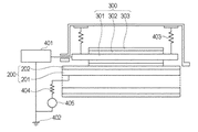
図5は、直流電圧連続印加試験を説明するための図である。
まず、支持体201上に導電層202のみを形成した状態、もしくは、電子写真感光体から導電層202上の各層を剥離して支持体201上に導電層202のみを残した状態のもの(以下「試験用サンプル」ともいう。)200と、芯金301、弾性層302および表面層303を有する導電性ローラー300とを、両者の軸が平行になるように当接させる。その際、導電性ローラー300の芯金301の両端には、バネ403にて500gの荷重を与える。導電性ローラー300の芯金301を直流電源401につなぎ、試験用サンプル200の支持体201をアース402につなぐ。直流電圧(直流成分)のみの電圧−1.0kVの定電圧を、導電性ローラー300に、導電層を流れる1分あたりの電流量の減少率が初めて1%以下になるまで連続して印加する。このようにして、直流電圧のみの電圧−1.0kVが導電層202に連続印加される。図5中、404は抵抗(100kΩ)であり、405は電流計である。通常、電流量の絶対値は電圧印加直後に最大電流量Iaに達する。その後、電流量の絶対値は減少し、その減少の程度は次第に緩やかになっていき、やがて飽和域(導電層を流れる1分あたりの電流量の減少率が1%以下)に達する。電圧印加後のある時間をt[分]とし、その1分後をt+1[分]とし、t[分]のときの電流量の絶対値をIt[μA]とし、t+1[分]のときの電流量の絶対値をIt+1[μA]とした場合、{(It−It+1)/It}×100が初めて1以下(1%以下)になったとき、t+1が「導電層を流れる1分あたりの電流量の減少率が初めて1%以下になったとき」にあたる。これを図示したものが図8である。この場合、Ib=It+1となる。
FIG. 5 is a diagram for explaining a DC voltage continuous application test.
First, a state in which only the
図6は、上記試験に用いられる導電性ローラー300の概略構成を示す図である。
導電性ローラー300は、導電性ローラー300の抵抗を制御する中抵抗の表面層303と、試験用サンプル200の表面と均一なニップを形成するために必要な弾性を有する導電性の弾性層302と、芯金301とで構成される。
FIG. 6 is a diagram illustrating a schematic configuration of the
The
直流成分のみの電圧−1.0kVを試験用サンプル200の導電層202に安定的に連続印加するためには、試験用サンプル200と導電性ローラー300とのニップを一定に保つことが必要である。ニップを一定に保つためには、導電性ローラー300の弾性層302の硬度とバネ403の強度を適宜調整すればよい。その他、ニップ調整用の機構を設けてもよい。
In order to stably apply a voltage of only a direct current component of −1.0 kV to the
導電性ローラー300としては、以下のようにして作製したものを用いた。以下の「部」は「質量部」を意味する。
As the
芯金301としては、直径6mmのステンレス製の芯金を用いた。
As the
次に、弾性層302を以下の方法で芯金301上に形成した。
Next, the
以下の材料を50℃に調節した密閉型ミキサーにて10分間混練することによって、原料コンパウンドを調製した。 A raw material compound was prepared by kneading the following materials in a closed mixer adjusted to 50 ° C. for 10 minutes.
エピクロルヒドリンゴム三元共重合体(エピクロルヒドリン:エチレンオキサイド:アリルグリシジルエーテル=40mol%:56mol%:4mol%);100部
炭酸カルシウム(軽質);30部
脂肪族ポリエステル(可塑剤);5部
ステアリン酸亜鉛;1部
2−メルカプトベンズイミダゾール(老化防止剤);0.5部
酸化亜鉛;5部
下記式で示される四級アンモニウム塩;2部

このコンパウンドに、原料のゴムとしての上記エピクロルヒドリンゴム三元共重合体100部に対して、加硫剤としての硫黄1部、加硫促進剤としてのジベンゾチアジルスルフィド1部およびテトラメチルチウラムモノスルフィド0.5部を加え、20℃に冷却した2本ロール機にて10分間混練した。 To this compound, 100 parts of the above epichlorohydrin rubber terpolymer as a raw rubber, 1 part of sulfur as a vulcanizing agent, 1 part of dibenzothiazyl sulfide as a vulcanization accelerator and tetramethylthiuram monosulfide 0.5 part was added, and it knead | mixed for 10 minutes with the 2-roll machine cooled to 20 degreeC.
この混練にて得られたコンパウンドを、芯金301上に、外径15mmのローラー状になるように押し出し成型機にて成型し、加熱蒸気加硫した後、外径が10mmになるように研磨加工を行うことによって、芯金301上に弾性層302が形成されてなる弾性ローラーを得た。この際、研磨加工においては、幅広研磨方式を採用した。弾性ローラーの長さは232mmとした。
The compound obtained by this kneading is molded on the
次に、弾性層302上に表面層303を以下の方法で被覆形成した。
Next, the
以下の材料を用いて、ガラス瓶を容器として混合溶液を調製した。
カプローラクトン変性アクリルポリオール溶液;100部
メチルイソブチルケトン;250部
導電性の酸化スズ(SnO2)(トリフルオロプロピルトリメトキシシラン処理品、平均粒径:0.05μm、粉体抵抗率:1×10³Ω・cm);250部
疎水性シリカ(ジメチルポリシロキサン処理品、平均粒径:0.02μm、粉体抵抗率:1×10¹⁶Ω・cm);3部
変性ジメチルシリコーンオイル;0.08部
架橋PMMA粒子(平均粒径:4.98μm);80部
Using the following materials, a mixed solution was prepared using a glass bottle as a container.
Caprolactone modified acrylic polyol solution; 100 parts methyl isobutyl ketone; 250 parts Conductive tin oxide (SnO 2 ) (treated with trifluoropropyltrimethoxysilane, average particle size: 0.05 μm, powder resistivity: 1 × 10 3 Ω · cm); 250 parts Hydrophobic silica (dimethylpolysiloxane-treated product, average particle size: 0.02 μm, powder resistivity: 1 × 10 16 Ω · cm); 3 parts modified dimethyl silicone oil; 08 parts crosslinked PMMA particles (average particle size: 4.98 μm); 80 parts
この混合溶液をペイントシェーカー分散機に入れ、分散メディアとしての平均粒径0.8mmのガラスビーズを充填率80%になるように充填し、18時間分散処理することによって、分散溶液を調製した。 This mixed solution was put in a paint shaker disperser, filled with glass beads having an average particle diameter of 0.8 mm as a dispersion medium so as to have a filling rate of 80%, and dispersed for 18 hours to prepare a dispersion solution.
この分散溶液に、ヘキサメチレンジイソシアネート(HDI)とイソホロンジイソシアネート(IPDI)の各ブタノンオキシムブロック体1:1の混合物を、NCO/OH=1.0となるように添加することによって、表面層用塗布液を調製した。 To this dispersion solution, a mixture of hexamethylene diisocyanate (HDI) and isophorone diisocyanate (IPDI) each butanone oxime block body 1: 1 was added so that NCO / OH = 1.0. A liquid was prepared.
この表面層用塗布液を上記弾性ローラーの弾性層302上に浸漬塗布法にて2回塗布し、これを風乾させた後、1時間160℃で乾燥させることによって、表面層303を形成した。
This surface layer coating solution was applied twice on the
このようにして、芯金301、弾性層302および表面層303を有する導電性ローラー300を作製した。作製した導電性ローラーの抵抗を以下のようにして測定したところ、1.0×10⁵Ωであった。
In this way, a
図7は、導電性ローラーの抵抗の測定方法を説明するための図である。 FIG. 7 is a diagram for explaining a method of measuring the resistance of the conductive roller.
導電性ローラーの抵抗は、常温常湿(23℃/50%RH)環境下において測定する。ステンレススチール製の円筒電極515と導電性ローラー300とを、両者の軸が平行になるように当接させる。その際、導電性ローラーの芯金(不図示)の両端には、500gの荷重を与える。円筒電極515としては、上記試験用サンプルと同じ外径のものを選択し、使用する。このような当接状態のまま、円筒電極515を200rpmの回転数で駆動回転させ、同じ速度で導電性ローラー300を従動回転させ、円筒電極515に外部電源53から−200Vを印加する。その際に導電性ローラー300に流れる電流値から算出される抵抗を、導電性ローラー300の抵抗とする。なお、図7中、516は抵抗であり、517はレコーダーである。
The resistance of the conductive roller is measured in a normal temperature and normal humidity (23 ° C./50% RH) environment. The stainless steel cylindrical electrode 515 and the
以下に、具体的な実施例を挙げて本発明をさらに詳細に説明する。ただし、本発明はこれらに限定されるものではない。なお、実施例および比較例中の「部」は「質量部」を意味する。 Hereinafter, the present invention will be described in more detail with reference to specific examples. However, the present invention is not limited to these. In the examples and comparative examples, “part” means “part by mass”.
また、実施例および比較例中で使用した各種酸化スズで被覆されている金属酸化物粒子の中で、芯材粒子が酸化チタン粒子であるものの酸化チタン粒子(芯材粒子)は、すべて硫酸法により製造された純度98.0%、BET値が7.2m2/gの球状のものである。芯材粒子が酸化チタン粒子である各種酸化スズで被覆されている金属酸化物粒子(複合粒子)の被覆率は、すべて45質量%である。また、芯材粒子が酸化チタン粒子である各種酸化スズで被覆されている金属酸化物粒子(複合粒子)のうち、粉体抵抗率5.0×102Ω・cmのもののBET値は、25.0m2/gである。また、芯材粒子が酸化チタン粒子である各種酸化スズで被覆されている金属酸化物粒子(複合粒子)のうち、粉体抵抗率1.0×103Ω・cmのもののBET値は、26.0m2/gである。また、芯材粒子が酸化チタン粒子である各種酸化スズで被覆されている金属酸化物粒子(複合粒子)のうち、粉体抵抗率3.0×103Ω・cmのもののBET値は、26.5m2/gである。また、芯材粒子が酸化チタン粒子である各種酸化スズで被覆されている金属酸化物粒子(複合粒子)のうち、粉体抵抗率5.0×103Ω・cmのもののBET値は、27.0m2/gである。また、芯材粒子が酸化チタン粒子である各種酸化スズで被覆されている金属酸化物粒子(複合粒子)のうち、粉体抵抗率1.0×104Ω・cmのもののBET値は、28.0m2/gである。また、芯材粒子が酸化チタン粒子である各種酸化スズで被覆されている金属酸化物粒子(複合粒子)のうち、粉体抵抗率5.0×104Ω・cmのもののBET値は、29.0m2/gである。また、芯材粒子が酸化チタン粒子である各種酸化スズで被覆されている金属酸化物粒子(複合粒子)のうち、粉体抵抗率1.0×105Ω・cmのもののBET値は、30.0m2/gである。また、芯材粒子が酸化チタン粒子である各種酸化スズで被覆されている金属酸化物粒子(複合粒子)のうち、粉体抵抗率5.0×105Ω・cmのもののBET値は、30.5m2/gである。 Of the metal oxide particles coated with various tin oxides used in Examples and Comparative Examples, all of the titanium oxide particles (core material particles) whose core material particles are titanium oxide particles are sulfuric acid methods. Manufactured in a spherical shape with a purity of 98.0% and a BET value of 7.2 m 2 / g. The coverage of the metal oxide particles (composite particles) in which the core particles are coated with various tin oxides that are titanium oxide particles is 45% by mass. Of the metal oxide particles (composite particles) coated with various tin oxides whose core material particles are titanium oxide particles, those having a powder resistivity of 5.0 × 10 2 Ω · cm have a BET value of 25 0.0 m 2 / g. Of the metal oxide particles (composite particles) coated with various tin oxides whose core material particles are titanium oxide particles, those having a powder resistivity of 1.0 × 10 3 Ω · cm have a BET value of 26 0.0 m 2 / g. Of the metal oxide particles (composite particles) coated with various tin oxides whose core material particles are titanium oxide particles, those having a powder resistivity of 3.0 × 10 3 Ω · cm have a BET value of 26 0.5 m 2 / g. Of the metal oxide particles (composite particles) coated with various tin oxides whose core material particles are titanium oxide particles, those having a powder resistivity of 5.0 × 10 3 Ω · cm have a BET value of 27 0.0 m 2 / g. Of the metal oxide particles (composite particles) coated with various tin oxides whose core material particles are titanium oxide particles, those having a powder resistivity of 1.0 × 10 4 Ω · cm have a BET value of 28 0.0 m 2 / g. Of the metal oxide particles (composite particles) coated with various tin oxides whose core material particles are titanium oxide particles, those having a powder resistivity of 5.0 × 10 4 Ω · cm have a BET value of 29 0.0 m 2 / g. Of the metal oxide particles (composite particles) coated with various tin oxides whose core material particles are titanium oxide particles, those having a powder resistivity of 1.0 × 10 5 Ω · cm have a BET value of 30. 0.0 m 2 / g. Of the metal oxide particles (composite particles) coated with various tin oxides whose core material particles are titanium oxide particles, those having a powder resistivity of 5.0 × 10 5 Ω · cm have a BET value of 30. 0.5 m 2 / g.
また、実施例および比較例中で使用した各種酸化スズで被覆されている金属酸化物粒子の中で、芯材粒子が酸化スズ粒子であるものの酸化スズ粒子(芯材粒子)は、すべて純度99.9%、BET値が9.5m2/gの球状のものである。芯材粒子が酸化スズ粒子である各種酸化スズで被覆されている金属酸化物粒子(複合粒子)の被覆率は、すべて40質量%である。また、芯材粒子が酸化スズ粒子である各種酸化スズで被覆されている金属酸化物粒子(複合粒子)のうち、粉体抵抗率5.0×102Ω・cmのもののBET値は、28.0m2/gである。また、芯材粒子が酸化スズ粒子である各種酸化スズで被覆されている金属酸化物粒子(複合粒子)のうち、粉体抵抗率1.0×103Ω・cmのもののBET値は、29.0m2/gである。また、芯材粒子が酸化スズ粒子である各種酸化スズで被覆されている金属酸化物粒子(複合粒子)のうち、粉体抵抗率3.0×103Ω・cmのもののBET値は、29.5m2/gである。また、芯材粒子が酸化スズ粒子である各種酸化スズで被覆されている金属酸化物粒子(複合粒子)のうち、粉体抵抗率5.0×103Ω・cmのもののBETが30.0m2/gである。また、芯材粒子が酸化スズ粒子である各種酸化スズで被覆されている金属酸化物粒子(複合粒子)のうち、粉体抵抗率1.0×104Ω・cmのもののBET値は、31.0m2/gである。また、芯材粒子が酸化スズ粒子である各種酸化スズで被覆されている金属酸化物粒子(複合粒子)のうち、粉体抵抗率5.0×104Ω・cmのもののBET値は、32.0m2/gである。また、芯材粒子が酸化スズ粒子である各種酸化スズで被覆されている金属酸化物粒子(複合粒子)のうち、粉体抵抗率1.0×105Ω・cmのもののBET値は、33.0m2/gである。また、芯材粒子が酸化スズ粒子である各種酸化スズで被覆されている金属酸化物粒子(複合粒子)のうち、粉体抵抗率5.0×105Ω・cmのもののBET値は、33.5m2/gである。 Of the metal oxide particles coated with various tin oxides used in the examples and comparative examples, the tin oxide particles (core material particles) whose core material particles are tin oxide particles have a purity of 99. .9% and spherical with a BET value of 9.5 m 2 / g. The coverage of metal oxide particles (composite particles) coated with various tin oxides whose core material particles are tin oxide particles is 40% by mass. Of the metal oxide particles (composite particles) coated with various tin oxides whose core material particles are tin oxide particles, those having a powder resistivity of 5.0 × 10 2 Ω · cm have a BET value of 28 0.0 m 2 / g. Of the metal oxide particles (composite particles) coated with various tin oxides whose core material particles are tin oxide particles, those having a powder resistivity of 1.0 × 10 3 Ω · cm have a BET value of 29 0.0 m 2 / g. Of the metal oxide particles (composite particles) coated with various tin oxides whose core material particles are tin oxide particles, those having a powder resistivity of 3.0 × 10 3 Ω · cm have a BET value of 29 0.5 m 2 / g. Of the metal oxide particles (composite particles) coated with various tin oxides whose core material particles are tin oxide particles, those having a powder resistivity of 5.0 × 10 3 Ω · cm have a BET of 30.0 m. 2 / g. Of the metal oxide particles (composite particles) coated with various tin oxides whose core material particles are tin oxide particles, those having a powder resistivity of 1.0 × 10 4 Ω · cm have a BET value of 31. 0.0 m 2 / g. Of the metal oxide particles (composite particles) coated with various tin oxides whose core material particles are tin oxide particles, those having a powder resistivity of 5.0 × 10 4 Ω · cm have a BET value of 32. 0.0 m 2 / g. Of the metal oxide particles (composite particles) coated with various tin oxides whose core material particles are tin oxide particles, those having a powder resistivity of 1.0 × 10 5 Ω · cm have a BET value of 33. 0.0 m 2 / g. Of the metal oxide particles (composite particles) coated with various tin oxides whose core material particles are tin oxide particles, those having a powder resistivity of 5.0 × 10 5 Ω · cm have a BET value of 33. 0.5 m 2 / g.
また、実施例および比較例中で使用した各種酸化スズで被覆されている金属酸化物粒子の中で、芯材粒子が酸化亜鉛粒子であるものの酸化亜鉛粒子(芯材粒子)は、すべて純度98.0%、BET値8.3m2/gの球状のものである。芯材粒子が酸化亜鉛粒子である各種酸化スズで被覆されている金属酸化物粒子(複合粒子)の被覆率は、すべて37質量%である。また、芯材粒子が酸化亜鉛粒子である各種酸化スズで被覆されている金属酸化物粒子(複合粒子)のうち、粉体抵抗率5.0×102Ω・cmのもののBET値は、26.0m2/gである。また、芯材粒子が酸化亜鉛粒子である各種酸化スズで被覆されている金属酸化物粒子(複合粒子)のうち、粉体抵抗率1.0×103Ω・cmのもののBET値は、27.0m2/gである。また、芯材粒子が酸化亜鉛粒子である各種酸化スズで被覆されている金属酸化物粒子(複合粒子)のうち、粉体抵抗率3.0×103Ω・cmのもののBET値は、27.5m2/gである。また、芯材粒子が酸化亜鉛粒子である各種酸化スズで被覆されている金属酸化物粒子(複合粒子)のうち、粉体抵抗率5.0×103Ω・cmのもののBET値は、28.0m2/gである。また、芯材粒子が酸化亜鉛粒子である各種酸化スズで被覆されている金属酸化物粒子(複合粒子)のうち、粉体抵抗率1.0×104Ω・cmのもののBET値は、29.0m2/gである。また、芯材粒子が酸化亜鉛粒子である各種酸化スズで被覆されている金属酸化物粒子(複合粒子)のうち、粉体抵抗率5.0×104Ω・cmのもののBET値は、30.0m2/gである。また、芯材粒子が酸化亜鉛粒子である各種酸化スズで被覆されている金属酸化物粒子(複合粒子)のうち、粉体抵抗率1.0×105Ω・cmのもののBET値は、31.0m2/gである。また、芯材粒子が酸化亜鉛粒子である各種酸化スズで被覆されている金属酸化物粒子(複合粒子)のうち、粉体抵抗率5.0×105Ω・cmのもののBET値は、31.5m2/gである。 Of the metal oxide particles coated with various tin oxides used in Examples and Comparative Examples, the zinc oxide particles (core material particles) whose core material particles are zinc oxide particles have a purity of 98. It is spherical with a 0.0% BET value of 8.3 m 2 / g. The coverage of the metal oxide particles (composite particles) in which the core material particles are coated with various tin oxides that are zinc oxide particles is 37% by mass. Of the metal oxide particles (composite particles) coated with various tin oxides whose core material particles are zinc oxide particles, those having a powder resistivity of 5.0 × 10 2 Ω · cm have a BET value of 26 0.0 m 2 / g. Of the metal oxide particles (composite particles) coated with various tin oxides whose core material particles are zinc oxide particles, those having a powder resistivity of 1.0 × 10 3 Ω · cm have a BET value of 27 0.0 m 2 / g. Of the metal oxide particles (composite particles) coated with various tin oxides whose core material particles are zinc oxide particles, those having a powder resistivity of 3.0 × 10 3 Ω · cm have a BET value of 27 0.5 m 2 / g. Of the metal oxide particles (composite particles) coated with various tin oxides whose core material particles are zinc oxide particles, those having a powder resistivity of 5.0 × 10 3 Ω · cm have a BET value of 28 0.0 m 2 / g. Of the metal oxide particles (composite particles) coated with various tin oxides whose core material particles are zinc oxide particles, those having a powder resistivity of 1.0 × 10 4 Ω · cm have a BET value of 29 0.0 m 2 / g. Of the metal oxide particles (composite particles) coated with various tin oxides whose core material particles are zinc oxide particles, those having a powder resistivity of 5.0 × 10 4 Ω · cm have a BET value of 30 0.0 m 2 / g. Of the metal oxide particles (composite particles) coated with various tin oxides whose core material particles are zinc oxide particles, those having a powder resistivity of 1.0 × 10 5 Ω · cm have a BET value of 31. 0.0 m 2 / g. Of the metal oxide particles (composite particles) coated with various tin oxides whose core material particles are zinc oxide particles, those having a powder resistivity of 5.0 × 10 5 Ω · cm have a BET value of 31. 0.5 m 2 / g.
また、実施例中で使用した各種酸化スズで被覆されている金属酸化物粒子の中で、芯材粒子が酸化ジルコニウム粒子であるものの酸化ジルコニウム粒子(芯材粒子)は、すべて純度99.0%、BET値8.3m2/gの球状のものである。芯材粒子が酸化ジルコニア粒子である各種酸化スズで被覆されている金属酸化物粒子(複合粒子)の被覆率は、すべて36質量%である。また、芯材粒子が酸化ジルコニア粒子である各種酸化スズで被覆されている金属酸化物粒子(複合粒子)のうち、粉体抵抗率1.0×103Ω・cmのもののBET値は、27.0m2/gである。また、芯材粒子が酸化ジルコニア粒子である各種酸化スズで被覆されている金属酸化物粒子(複合粒子)のうち、粉体抵抗率1.0×105Ω・cmのもののBET値は、31.0m2/gである。 Of the metal oxide particles coated with various tin oxides used in the examples, the zirconium oxide particles (core particles) whose core particles are zirconium oxide particles have a purity of 99.0%. , Spherical with a BET value of 8.3 m 2 / g. The coverage of the metal oxide particles (composite particles) in which the core material particles are coated with various tin oxides, which are zirconia oxide particles, is 36% by mass. Of the metal oxide particles (composite particles) coated with various tin oxides whose core material particles are zirconia oxide particles, those having a powder resistivity of 1.0 × 10 3 Ω · cm have a BET value of 27 0.0 m 2 / g. Of the metal oxide particles (composite particles) coated with various tin oxides whose core material particles are zirconia oxide particles, those having a powder resistivity of 1.0 × 10 5 Ω · cm have a BET value of 31. 0.0 m 2 / g.
なお、以下の導電層用塗布液1で使用したニオブがドープされている酸化スズで被覆されている酸化チタン粒子(複合粒子)は、焼成温度650℃で焼成したものである。なお、焼成温度を上昇させるに従い、各種酸化スズで被覆されている金属酸化物粒子(複合粒子)の粉体抵抗率は低下する傾向にあり、BET値は低下する傾向にある。実施例および比較例中で使用した各種酸化スズで被覆されている金属酸化物粒子(複合粒子)の粉体抵抗率についても、焼成温度を変更することによって調整した。 In addition, the titanium oxide particles (composite particles) coated with niobium-doped tin oxide used in the following conductive layer coating solution 1 were fired at a firing temperature of 650 ° C. As the firing temperature is increased, the powder resistivity of metal oxide particles (composite particles) coated with various tin oxides tends to decrease, and the BET value tends to decrease. The powder resistivity of the metal oxide particles (composite particles) coated with various tin oxides used in Examples and Comparative Examples was also adjusted by changing the firing temperature.
また、実施例および比較例中の酸化スズは「SnO2」であり、酸化チタンは「TiO2」、酸化亜鉛は「ZnO」であり、酸化ジルコニウムは「ZrO2」である。 Further, tin oxide in Examples and Comparative Examples is “SnO 2 ”, titanium oxide is “TiO 2 ”, zinc oxide is “ZnO”, and zirconium oxide is “ZrO 2 ”.
〈導電層用塗布液の調製例〉
(導電層用塗布液1の調製例)
金属酸化物粒子としてのニオブがドープされている酸化スズ(SnO2)で被覆されている酸化チタン(TiO2)粒子(粉体抵抗率:1.0×10³Ω・cm、平均一次粒径:250nm)207部、結着材料としてのフェノール樹脂(フェノール樹脂のモノマー/オリゴマー)(商品名:プライオーフェンJ−325、大日本インキ化学工業(株)製、樹脂固形分:60質量%)144部、および、溶剤としての1−メトキシ−2−プロパノール98部を、直径0.8mmのガラスビーズ450部を用いたサンドミルに入れ、回転数:2000rpm、分散処理時間:2.5時間、冷却水の設定温度:18℃の条件で分散処理を行い、分散液を得た。
<Example of preparation of coating solution for conductive layer>
(Preparation example of coating liquid 1 for conductive layer)
Titanium oxide (TiO 2 ) particles coated with tin oxide (SnO 2 ) doped with niobium as metal oxide particles (powder resistivity: 1.0 × 10 3 Ω · cm, average primary particle size : 207 parts, phenol resin (monomer / oligomer of phenol resin) as a binder (trade name: PRIOFEN J-325, manufactured by Dainippon Ink & Chemicals, Inc., resin solid content: 60% by mass) 144 And 98 parts of 1-methoxy-2-propanol as a solvent are put in a sand mill using 450 parts of glass beads having a diameter of 0.8 mm, the rotational speed is 2000 rpm, the dispersion treatment time is 2.5 hours, and the cooling water is used. The dispersion treatment was performed under the condition of a set temperature of 18 ° C. to obtain a dispersion.
この分散液からメッシュでガラスビーズを取り除いた後、分散液に表面粗し付与材としてのシリコーン樹脂粒子(商品名:トスパール120、モメンティブ・パフォーマンス・マテリアルズ社(旧・GE東芝シリコーン(株))製、平均粒径:2μm)13.8部、レベリング剤としてのシリコーンオイル(商品名:SH28PA、東レ・ダウコーニング(株)(旧・東レ・ダウコーニング・シリコーン(株))製)0.014部、メタノール6部、および、1−メトキシ−2−プロパノール6部を添加して攪拌することによって、導電層用塗布液1を調製した。 After removing the glass beads from the dispersion with a mesh, the surface of the dispersion is roughened with silicone resin particles (product name: Tospearl 120, Momentive Performance Materials (former GE Toshiba Silicone)) Manufactured, average particle size: 2 μm) 13.8 parts, leveling agent silicone oil (trade name: SH28PA, manufactured by Toray Dow Corning Co., Ltd. (formerly Toray Dow Corning Silicone Co., Ltd.)) 0.014 The coating liquid 1 for conductive layers was prepared by adding and stirring 6 parts of methanol, 6 parts of methanol, and 6 parts of 1-methoxy-2-propanol.
導電層用塗布液1における金属酸化物粒子(ニオブがドープされている酸化スズ(SnO2)で被覆されている酸化チタン(TiO2)粒子)の平均粒径は、0.29μmであった。 The average particle diameter of the metal oxide particles (titanium oxide (TiO 2 particles coated with niobium-doped tin oxide (SnO 2 ))) in the conductive layer coating solution 1 was 0.29 μm.
(導電層用塗布液2〜110およびC1〜C101の調製例)
導電層用塗布液の調製の際に用いた金属酸化物粒子の種類、粉体抵抗率および量(部数)、結着材料としてのフェノール樹脂(フェノール樹脂のモノマー/オリゴマー)の量(部数)、ならびに、分散処理時間を、それぞれ表1〜表9に示すようにした以外は、導電層用塗布液1の調製例と同様の操作で、導電層用塗布液2〜110およびC1〜C101を調製した。導電層用塗布液2〜110およびC1〜C101における金属酸化物粒子の平均粒径を、それぞれ表1〜表9に示す。
(Preparation examples of conductive
Type of metal oxide particles used in the preparation of the coating liquid for the conductive layer, powder resistivity and amount (parts), amount of phenol resin (monomer / oligomer of phenol resin) as a binder (parts), In addition, the conductive
〈電子写真感光体の製造例〉
(電子写真感光体1の製造例)
押し出し工程および引き抜き工程を含む製造方法により製造された、長さ246mm、直径24mmのアルミニウムシリンダー(JIS−A3003、アルミニウム合金)を支持体とした。
<Example of production of electrophotographic photoreceptor>
(Example of production of electrophotographic photoreceptor 1)
An aluminum cylinder (JIS-A3003, aluminum alloy) having a length of 246 mm and a diameter of 24 mm manufactured by a manufacturing method including an extrusion process and a drawing process was used as a support.
常温常湿(23℃/50%RH)環境下で、導電層用塗布液1を支持体上に浸漬塗布し、これを30分間140℃で乾燥および熱硬化させることによって、膜厚が30μmの導電層を形成した。導電層の体積抵抗率を前述の方法で測定したところ、5.0×109Ω・cmであった。また、導電層の最大電流量Iaおよび電流量Ibを前述の方法で測定したところ、最大電流量Iaは5200μAであり、電流量Ibは30μAであった。 In a room temperature and normal humidity (23 ° C./50% RH) environment, the conductive layer coating solution 1 is dip-coated on a support, and this is dried and thermally cured at 140 ° C. for 30 minutes, whereby the film thickness is 30 μm. A conductive layer was formed. When the volume resistivity of the conductive layer was measured by the method described above, it was 5.0 × 10 9 Ω · cm. Further, when the maximum current amount Ia and the current amount Ib of the conductive layer were measured by the above-described method, the maximum current amount Ia was 5200 μA, and the current amount Ib was 30 μA.
次に、N−メトキシメチル化ナイロン(商品名:トレジンEF−30T、ナガセケムテックス(株)(旧・帝国化学産業(株))製)4.5部および共重合ナイロン樹脂(商品名:アミランCM8000、東レ(株)製)1.5部を、メタノール65部/n−ブタノール30部の混合溶剤に溶解させることによって、下引き層用塗布液を調製した。この下引き層用塗布液を導電層上に浸漬塗布し、これを6分間70℃で乾燥させることによって、膜厚が0.85μmの下引き層を形成した。 Next, N-methoxymethylated nylon (trade name: Toresin EF-30T, Nagase ChemteX Co., Ltd. (former Teikoku Chemical Industry Co., Ltd.)) 4.5 parts and copolymer nylon resin (trade name: Amilan) CM8000 (manufactured by Toray Industries, Inc.) was dissolved in a mixed solvent of 65 parts of methanol / 30 parts of n-butanol to prepare an undercoat layer coating solution. The undercoat layer coating solution was dip-coated on the conductive layer, and dried at 70 ° C. for 6 minutes to form an undercoat layer having a thickness of 0.85 μm.
次に、CuKα特性X線回折におけるブラッグ角(2θ±0.2°)の7.5°、9.9°、16.3°、18.6°、25.1°および28.3°に強いピークを有する結晶形のヒドロキシガリウムフタロシアニン結晶(電荷発生物質)10部、ポリビニルブチラール(商品名:エスレックBX−1、積水化学工業(株)製)5部およびシクロヘキサノン250部を、直径0.8mmのガラスビーズを用いたサンドミルに入れ、分散処理時間:3時間の条件で分散処理を行い、次に、酢酸エチル250部を加えることによって、電荷発生層用塗布液を調製した。この電荷発生層用塗布液を下引き層上に浸漬塗布し、これを10分間100℃で乾燥させることによって、膜厚が0.12μmの電荷発生層を形成した。 Next, the Bragg angles (2θ ± 0.2 °) in CuKα characteristic X-ray diffraction are 7.5 °, 9.9 °, 16.3 °, 18.6 °, 25.1 ° and 28.3 °. A crystalline form of hydroxygallium phthalocyanine crystal (charge generating substance) having a strong peak, 10 parts, polyvinyl butyral (trade name: ESREC BX-1, manufactured by Sekisui Chemical Co., Ltd.), and 250 parts of cyclohexanone, 0.8 mm in diameter In a sand mill using glass beads, a dispersion treatment was performed under the condition of dispersion treatment time: 3 hours, and then 250 parts of ethyl acetate was added to prepare a charge generation layer coating solution. This coating solution for charge generation layer was dip-coated on the undercoat layer and dried at 100 ° C. for 10 minutes to form a charge generation layer having a thickness of 0.12 μm.
次に、下記式(CT−1)で示されるアミン化合物(電荷輸送物質)4.8部および下記式(CT−2)で示されるアミン化合物(電荷輸送物質)3.2部、
このようにして、電荷輸送層が表面層である電子写真感光体1を製造した。 Thus, an electrophotographic photoreceptor 1 having a charge transport layer as a surface layer was produced.
(電子写真感光体2〜110およびC1〜C101の製造例)
電子写真感光体の製造の際に用いた導電層用塗布液を、導電層用塗布液1から、それぞれ導電層用塗布液2〜110、C1〜C101に変更した以外は、電子写真感光体1の製造例と同様の操作で、電荷輸送層が表面層である電子写真感光体2〜110およびC1〜C101を製造した。なお、電子写真感光体2〜110およびC1〜C101の導電層の体積抵抗率ならびに最大電流量Iaおよび電流量Ibに関しても、電子写真感光体1の導電層と同様、前述の方法で測定した。その結果を表10〜表15に示す。なお、電子写真感光体1〜110およびC1〜C101について、導電層の体積抵抗率の測定の際に、それらの導電層の表面を光学顕微鏡で観察したところ、電子写真感光体C8、C10、C20、C22、C32、C34、C44、C46、C56、C58、C68、C70の導電層に関しては、クラックの発生が確認された。
(Examples of production of electrophotographic photoreceptors 2-110 and C1-C101)
The electrophotographic photosensitive member 1 except that the conductive layer coating solution used in the production of the electrophotographic photosensitive member was changed from the conductive layer coating solution 1 to the conductive
(実施例1〜110および比較例1〜101)
電子写真感光体1〜110およびC1〜C101を、それぞれヒューレットパッカード社製のレーザービームプリンター(商品名:HP Laserjet P1505)に装着して、低温低湿(15℃/10%RH)環境下にて通紙耐久試験を行い、画像の評価を行った。通紙耐久試験では、印字率2%の文字画像をレター紙に1枚ずつ出力する間欠モードでプリント操作を行い、3000枚の画像出力を行った。
(Examples 1-110 and Comparative Examples 1-101)
The electrophotographic photosensitive members 1 to 110 and C1 to C101 are respectively attached to a laser beam printer (trade name: HP Laserjet P1505) manufactured by Hewlett-Packard Co., and passed under a low temperature and low humidity (15 ° C./10% RH) environment. A paper durability test was conducted to evaluate the image. In the paper passing durability test, a printing operation was performed in an intermittent mode in which character images with a printing rate of 2% were output one by one on letter paper, and 3000 images were output.
そして、通紙耐久試験開始時、ならびに、1500枚画像出力終了後および3000枚画像出力終了後に各1枚の画像評価用のサンプル(1ドット桂馬パターンのハーフトーン画像)を出力した。1ドット桂馬パターンのハーフトーン画像とは、図9に示すパターンのハーフトーン画像である。 Then, one sample for image evaluation (halftone image of 1-dot Keima pattern) was output at the start of the paper passing durability test and after the end of output of the 1500 sheets and after the end of output of the 3000 sheets. The halftone image of the 1-dot Keima pattern is a halftone image of the pattern shown in FIG.
画像の評価の基準は以下のとおりである。結果を表16〜表21に示す。
A:リークの発生は全くなし。
B:リークが小さな黒点としてわずかに観測される。
C:リークが大きな黒点としてはっきり観測される。
D:リークが大きな黒点と短い横黒スジとして観測される。
E:リークが長い横黒スジとして観測される。
The criteria for image evaluation are as follows. The results are shown in Tables 16-21.
A: No leak occurred at all.
B: Leak is slightly observed as a small black spot.
C: Leak is clearly observed as a large black spot.
D: Leaks are observed as large black spots and short horizontal black stripes.
E: Leak is observed as a long black line.
また、通紙耐久試験開始時ならびに3000枚画像出力終了後の画像評価用のサンプルを出力した後に、帯電電位(暗部電位)と露光時の電位(明部電位)を測定した。電位測定は、白ベタ画像と黒ベタ画像を各1枚ずつ用いて行った。初期(通紙耐久試験開始時)の暗部電位をVd、初期(通紙耐久試験開始時)の明部電位をVlとした。3000枚画像出力終了後の暗部電位をVd’、3000枚画像出力終了後の明部電位をVl’とした。3000枚画像出力終了後の暗部電位Vd’と初期の暗部電位Vdとの差である暗部電位変動量△Vd(=|Vd’|−|Vd|)と、3000枚画像出力終了後の明部電位Vl’と初期の明部電位Vlとの差である明部電位変動量△Vl(=|Vl’|−|Vl|)とをそれぞれ求めた。結果を表16〜表21に示す。 Further, after outputting the sample for image evaluation at the start of the paper passing durability test and after the output of 3000 sheets of images, the charging potential (dark portion potential) and the potential during exposure (bright portion potential) were measured. The potential measurement was performed using one white solid image and one black solid image. The dark portion potential at the initial stage (at the start of the paper passing durability test) was Vd, and the bright portion potential at the initial stage (at the start of the paper passing durability test) was Vl. The dark portion potential after the output of the 3000 sheets of images was Vd ′, and the bright portion potential after the output of the 3000 sheets of images was set to Vl ′. Dark portion potential fluctuation amount ΔVd (= | Vd ′ | − | Vd |), which is the difference between the dark portion potential Vd ′ after the end of the 3000 sheet image output and the initial dark portion potential Vd, and the bright portion after the 3000 sheet image output ends. The bright part potential fluctuation amount ΔVl (= | Vl ′ | − | Vl |), which is the difference between the potential Vl ′ and the initial bright part potential Vl, was obtained. The results are shown in Tables 16-21.
(実施例111〜220および比較例102〜202)
上記の通紙耐久試験を行った電子写真感光体1〜110およびC1〜C101とは別に、もう1つずつ電子写真感光体1〜110およびC1〜C101を用意し、これらの針耐圧試験を以下のようにして行った。結果を表22および表23に示す。
(Examples 111 to 220 and Comparative Examples 102 to 202)
Separately from the electrophotographic photoreceptors 1-110 and C1-C101 subjected to the paper passing durability test, another electrophotographic photoreceptors 1-110 and C1-C101 are prepared one by one. I went as follows. The results are shown in Table 22 and Table 23.
図4に針耐圧試験装置を示す。針耐圧試験は、常温常湿(23℃/50%RH)環境下において行う。電子写真感光体1401の両端を固定台1402に載せ動かないように固定させる。電子写真感光体1401の表面に針電極1403の先端を接触させる。この針電極1403に、電圧を印加するための電源1404と、電流を測定するための電流計1405を、それぞれ接続する。電子写真感光体1401の支持体に接触する部分1406をアースに接続する。針電極1403から2秒間印加する電圧を0Vから10Vずつ上昇させ、針電極1403の先端が接触している電子写真感光体1401の内部でリークが発生し、電流計1405の値が10倍以上大きくなり始めた電圧を針耐圧値とする。この測定を、電子写真感光体1401の表面の5箇所について実施し、その平均値を測定した電子写真感光体1401の針耐圧値とする。
FIG. 4 shows a needle pressure test apparatus. The needle pressure resistance test is performed in a normal temperature and normal humidity (23 ° C./50% RH) environment. Both ends of the electrophotographic
1 電子写真感光体
2 軸
3 帯電手段(一次帯電手段)
4 露光光(画像露光光)
5 現像手段
6 転写手段(転写ローラーなど)
7 クリーニング手段(クリーニングブレードなど)
8 定着手段
9 プロセスカートリッジ
10 案内手段
11 前露光光
P 転写材(紙など)
1 Electrophotographic
4 exposure light (image exposure light)
5 Developing means 6 Transfer means (transfer roller, etc.)
7 Cleaning means (cleaning blade, etc.)
8 Fixing means 9
Claims (6)
該導電層が、
(1)ニオブがドープされている酸化スズで被覆されている酸化チタン粒子、
(2)タンタルがドープされている酸化スズで被覆されている酸化チタン粒子、
(3)ニオブがドープされている酸化スズで被覆されている酸化スズ粒子、
(4)タンタルがドープされている酸化スズで被覆されている酸化スズ粒子、
(5)ニオブがドープされている酸化スズで被覆されている酸化亜鉛粒子、および
(6)タンタルがドープされている酸化スズで被覆されている酸化亜鉛粒子
からなる群から選択される少なくとも1種の金属酸化物粒子と、
結着材料と、を含有し、
該導電層の体積抵抗率が、1.0×10 8 Ω・cm以上5.0×10 12 Ω・cm以下であり、
該円筒状支持体と該導電層とから構成される試験用サンプルに対し、常温常湿(23℃/50%RH)環境下において、定電圧−1.0kVの直流電圧(直流成分のみ)を、
{(I t −I t+1 )/I t }×100
(電圧印加からt[分]後における電流量の絶対値をI t [μA]とし、t+1[分]後における電流量の絶対値をI t+1 [μA]とする)
が初めて1%以下になるまで連続して印加する試験を行った場合に、
該I t+1 が10μA以上となり、
該試験における最大電流量の絶対値(Ia)が6000μA以下となることを特徴とする電子写真感光体。 A cylindrical support, a conductive layer, an electrophotographic photosensitive member comprising a sensitive optical layer, in this order,
The conductive layer is
(1) Titanium oxide particles coated with tin oxide doped with niobium,
(2) Titanium oxide particles coated with tin oxide doped with tantalum,
(3) Tin oxide particles coated with tin oxide doped with niobium,
(4) Tin oxide particles coated with tin oxide doped with tantalum,
(5) zinc oxide particles coated with tin oxide doped with niobium, and
(6) Zinc oxide particles coated with tin oxide doped with tantalum
At least one metal oxide particle selected from the group consisting of:
Containing a binder material, a
The volume resistivity of the conductive layer is 1.0 × 10 8 Ω · cm to 5.0 × 10 12 Ω · cm,
A DC voltage (DC component only) of a constant voltage of −1.0 kV is applied to a test sample composed of the cylindrical support and the conductive layer in a normal temperature and normal humidity (23 ° C./50% RH) environment. ,
{(I t −I t + 1 ) / I t } × 100
(The absolute value of the current amount after t [minute] from the voltage application is I t [μA], and the absolute value of the current amount after t + 1 [minute] is I t + 1 [μA].)
When the test is continuously applied until the value becomes 1% or less for the first time,
The It + 1 becomes 10 μA or more,
An electrophotographic photosensitive member, wherein an absolute value (Ia) of a maximum current amount in the test is 6000 μA or less.
該導電層が、溶剤、結着材料、および、(1)〜(6)からなる群から選択される少なくとも1種の金属酸化物粒子を含有する導電層用塗布液を調製し、該円筒状支持体に塗布することで形成され、
該金属酸化物粒子の粉体抵抗率が、1.0×10³Ω・cm以上1.0×10⁵Ω・cm以下であり、
該導電層用塗布液における、該金属酸化物粒子(P)と結着材料(B)の質量比(P/B)が、1.5/1.0以上3.5/1.0以下であり、
該導電層の体積抵抗率が、1.0×10 8 Ω・cm以上5.0×10 12 Ω・cm以下であることを特徴とする電子写真感光体の製造方法。
(1)ニオブがドープされている酸化スズで被覆されている酸化チタン粒子
(2)タンタルがドープされている酸化スズで被覆されている酸化チタン粒子
(3)ニオブがドープされている酸化スズで被覆されている酸化スズ粒子
(4)タンタルがドープされている酸化スズで被覆されている酸化スズ粒子
(5)ニオブがドープされている酸化スズで被覆されている酸化亜鉛粒子
(6)タンタルがドープされている酸化スズで被覆されている酸化亜鉛粒子 A method for producing an electrophotographic photosensitive member having a cylindrical support, a conductive layer, and a photosensitive layer in this order ,
Conductive layer, a solvent, a binder material, and, (1) to a conductive layer coating liquid containing at least one metal oxide particles are selected from the group consisting of (6) was prepared, the cylindrical Formed by coating on a support,
Powder resistivity of the metal oxides particles, not more than 1.0 × 10 3 Ω · cm or more 1.0 × 10 5 Ω · cm,
In the conductive layer coating liquid, the weight ratio of the metal oxide particles (P) and binder material (B) (P / B) is 1.5 / 1.0 to 3.5 / 1.0 or less Oh it is,
The method for producing an electrophotographic photoreceptor, wherein the conductive layer has a volume resistivity of 1.0 × 10 8 Ω · cm to 5.0 × 10 12 Ω · cm .
(1) Titanium oxide particles coated with tin oxide doped with niobium
(2) Titanium oxide particles coated with tin oxide doped with tantalum
(3) Tin oxide particles coated with tin oxide doped with niobium
(4) Tin oxide particles coated with tin oxide doped with tantalum
(5) Zinc oxide particles coated with tin oxide doped with niobium
(6) Zinc oxide particles coated with tin oxide doped with tantalum
Priority Applications (5)
| Application Number | Priority Date | Filing Date | Title |
|---|---|---|---|
| JP2013053506A JP6074295B2 (en) | 2012-08-30 | 2013-03-15 | Electrophotographic photosensitive member, process cartridge and electrophotographic apparatus, and method for manufacturing electrophotographic photosensitive member |
| US13/972,688 US8980510B2 (en) | 2012-08-30 | 2013-08-21 | Electrophotographic photosensitive member, process cartridge and electrophotographic apparatus, and method for producing electrophotographic photosensitive member |
| KR1020130099487A KR101645777B1 (en) | 2012-08-30 | 2013-08-22 | Electrophotographic photosensitive member, process cartridge and electrophotographic apparatus, and method for producing electrophotographic photosensitive member |
| EP13182131.6A EP2703890B1 (en) | 2012-08-30 | 2013-08-29 | Electrophotographic photosensitive member, process cartridge and electrophotographic apparatus, and method for producing electrophotographic photosensitive member |
| CN201310386714.6A CN103676509B (en) | 2012-08-30 | 2013-08-30 | Electrophotographic photosensitive element and production method, handle box and electronic photographing device |
Applications Claiming Priority (7)
| Application Number | Priority Date | Filing Date | Title |
|---|---|---|---|
| JP2012189531 | 2012-08-30 | ||
| JP2012189531 | 2012-08-30 | ||
| JP2013012125 | 2013-01-25 | ||
| JP2013012117 | 2013-01-25 | ||
| JP2013012117 | 2013-01-25 | ||
| JP2013012125 | 2013-01-25 | ||
| JP2013053506A JP6074295B2 (en) | 2012-08-30 | 2013-03-15 | Electrophotographic photosensitive member, process cartridge and electrophotographic apparatus, and method for manufacturing electrophotographic photosensitive member |
Publications (3)
| Publication Number | Publication Date |
|---|---|
| JP2014160224A JP2014160224A (en) | 2014-09-04 |
| JP2014160224A5 JP2014160224A5 (en) | 2016-05-12 |
| JP6074295B2 true JP6074295B2 (en) | 2017-02-01 |
Family
ID=49035486
Family Applications (1)
| Application Number | Title | Priority Date | Filing Date |
|---|---|---|---|
| JP2013053506A Active JP6074295B2 (en) | 2012-08-30 | 2013-03-15 | Electrophotographic photosensitive member, process cartridge and electrophotographic apparatus, and method for manufacturing electrophotographic photosensitive member |
Country Status (5)
| Country | Link |
|---|---|
| US (1) | US8980510B2 (en) |
| EP (1) | EP2703890B1 (en) |
| JP (1) | JP6074295B2 (en) |
| KR (1) | KR101645777B1 (en) |
| CN (1) | CN103676509B (en) |
Cited By (1)
| Publication number | Priority date | Publication date | Assignee | Title |
|---|---|---|---|---|
| JP2015158598A (en) * | 2014-02-24 | 2015-09-03 | キヤノン株式会社 | Electrophotographic photoreceptor, process cartridge, and electrophotographic device |
Families Citing this family (22)
| Publication number | Priority date | Publication date | Assignee | Title |
|---|---|---|---|---|
| JP6108842B2 (en) | 2012-06-29 | 2017-04-05 | キヤノン株式会社 | Method for producing electrophotographic photosensitive member |
| JP6218502B2 (en) | 2012-08-30 | 2017-10-25 | キヤノン株式会社 | Electrophotographic photosensitive member, process cartridge, and electrophotographic apparatus |
| JP6425523B2 (en) * | 2013-12-26 | 2018-11-21 | キヤノン株式会社 | Electrophotographic photosensitive member, process cartridge and electrophotographic apparatus |
| JP6282138B2 (en) * | 2014-02-24 | 2018-02-21 | キヤノン株式会社 | Electrophotographic photosensitive member, process cartridge, and electrophotographic apparatus |
| JP6512841B2 (en) * | 2014-03-07 | 2019-05-15 | キヤノン株式会社 | Electrophotographic photosensitive member, method of manufacturing the same, process cartridge, and electrophotographic apparatus |
| DE112015003634B4 (en) | 2014-08-06 | 2021-12-09 | Denso Corporation | DISPLAY DEVICE FOR VEHICLE |
| US9625838B2 (en) * | 2014-11-28 | 2017-04-18 | Canon Kabushiki Kaisha | Electrophotographic apparatus, process cartridge, and image forming method |
| US9529284B2 (en) | 2014-11-28 | 2016-12-27 | Canon Kabushiki Kaisha | Process cartridge, image forming method, and electrophotographic apparatus |
| US9568846B2 (en) | 2014-11-28 | 2017-02-14 | Canon Kabushiki Kaisha | Electrophotographic photosensitive member, method for producing the same, process cartridge, and electrophotographic apparatus |
| CN105867080B (en) | 2015-02-09 | 2019-10-11 | 佳能株式会社 | Electrophotographic photosensitive element, handle box and electronic photographing device |
| JP6639256B2 (en) | 2016-02-10 | 2020-02-05 | キヤノン株式会社 | Electrophotographic apparatus and process cartridge |
| US10203617B2 (en) | 2017-02-28 | 2019-02-12 | Canon Kabushiki Kaisha | Electrophotographic photosensitive member, process cartridge and electrophotographic apparatus |
| EP3367167B1 (en) | 2017-02-28 | 2021-05-26 | Canon Kabushiki Kaisha | Electrophotographic photosensitive member, process cartridge, and electrophotographic apparatus |
| US10162278B2 (en) | 2017-02-28 | 2018-12-25 | Canon Kabushiki Kaisha | Electrophotographic photosensitive member, process cartridge and electrophotographic apparatus |
| US10216105B2 (en) | 2017-02-28 | 2019-02-26 | Canon Kabushiki Kaisa | Electrophotographic photosensitive member, process cartridge, and electrophotographic apparatus |
| JP6850205B2 (en) | 2017-06-06 | 2021-03-31 | キヤノン株式会社 | Electrophotographic photosensitive members, process cartridges and electrophotographic equipment |
| CN107248496B (en) * | 2017-06-07 | 2019-11-15 | 西安电子科技大学 | The modification method of ohmic contact regions square resistance |
| JP7118793B2 (en) * | 2018-07-31 | 2022-08-16 | キヤノン株式会社 | Electrophotographic photoreceptor, process cartridge and electrophotographic apparatus |
| JP7114403B2 (en) * | 2018-08-24 | 2022-08-08 | キヤノン株式会社 | Electrophotographic photoreceptor manufacturing method |
| JP7319858B2 (en) | 2018-08-24 | 2023-08-02 | キヤノン株式会社 | Electrophotographic photoreceptor, process cartridge and electrophotographic apparatus |
| JP7401256B2 (en) | 2019-10-18 | 2023-12-19 | キヤノン株式会社 | Electrophotographic equipment, process cartridges and cartridge sets |
| JP7330851B2 (en) | 2019-10-18 | 2023-08-22 | キヤノン株式会社 | Electrophotographic device, process cartridge, and cartridge set |
Family Cites Families (27)
| Publication number | Priority date | Publication date | Assignee | Title |
|---|---|---|---|---|
| JPH01150150A (en) | 1987-12-08 | 1989-06-13 | Matsushita Electric Ind Co Ltd | Electrophotographic sensitive body |
| JP2605789B2 (en) | 1988-03-30 | 1997-04-30 | 松下電器産業株式会社 | Electrophotographic photoreceptor |
| US5422210A (en) | 1991-03-18 | 1995-06-06 | Canon Kabushiki Kaisha | Electrophotographic photosensitive member and electrophotographic apparatus, device unit and facsimile machine using the same |
| US5385797A (en) | 1991-09-24 | 1995-01-31 | Canon Kabushiki Kaisha | Electrophotographic photosensitive member, and electrophotographic apparatus, device unit, and facsimile machine employing the same |
| US5357320A (en) | 1992-09-04 | 1994-10-18 | Canon Kabushiki Kaisha | Electrophotographic apparatus |
| US5455135A (en) | 1992-12-18 | 1995-10-03 | Canon Kabushiki Kaisha | Electrophotographic photosensitive member with overlayer and electrophotographic apparatus employing same |
| US6773856B2 (en) | 2001-11-09 | 2004-08-10 | Canon Kabushiki Kaisha | Electrophotographic photosensitive member, process cartridge, and electrophotographic apparatus |
| JP3938011B2 (en) * | 2002-10-30 | 2007-06-27 | キヤノン株式会社 | Electrophotographic photosensitive member and electrophotographic apparatus |
| JP4712288B2 (en) * | 2003-05-23 | 2011-06-29 | チタン工業株式会社 | White conductive powder and its application |
| US7245851B2 (en) | 2003-11-26 | 2007-07-17 | Canon Kabushiki Kaisha | Electrophotographic apparatus |
| US7276318B2 (en) | 2003-11-26 | 2007-10-02 | Canon Kabushiki Kaisha | Electrophotographic photosensitive member, and electrophotographic apparatus and process cartridge which make use of the same |
| JP4095589B2 (en) * | 2004-02-27 | 2008-06-04 | キヤノン株式会社 | Electrophotographic image forming apparatus and process cartridge |
| JP4702950B2 (en) * | 2005-03-28 | 2011-06-15 | キヤノン株式会社 | Electrophotographic photosensitive member, process cartridge and electrophotographic apparatus, and method for manufacturing electrophotographic photosensitive member |
| CN100578371C (en) | 2005-04-08 | 2010-01-06 | 佳能株式会社 | Electrophotographic photosensitive member, and process cartridge and electrophotographic apparatus with the electrophotographic photosensitive member |
| EP1960838B1 (en) | 2005-12-07 | 2011-05-11 | Canon Kabushiki Kaisha | Electrophotographic photosensitive member, process cartridge, and electrophotographic apparatus |
| CN101878453B (en) | 2007-12-04 | 2012-06-27 | 佳能株式会社 | Electrophotographic photoreceptor, process for producing electrophotographic photoreceptor, process cartridge, and electrophotographic apparatus |
| WO2010001818A1 (en) | 2008-07-02 | 2010-01-07 | 石原産業株式会社 | Tin oxide particles and process for production thereof |
| JP5264342B2 (en) * | 2008-07-24 | 2013-08-14 | キヤノン株式会社 | Image forming apparatus |
| JP5409209B2 (en) * | 2009-09-01 | 2014-02-05 | キヤノン株式会社 | Electrophotographic equipment |
| JP4743921B1 (en) | 2009-09-04 | 2011-08-10 | キヤノン株式会社 | Electrophotographic photosensitive member, process cartridge, and electrophotographic apparatus |
| JP4956654B2 (en) | 2009-09-04 | 2012-06-20 | キヤノン株式会社 | Electrophotographic photosensitive member, process cartridge, electrophotographic apparatus, and method of manufacturing electrophotographic photosensitive member |
| JP5054238B1 (en) | 2011-03-03 | 2012-10-24 | キヤノン株式会社 | Method for producing electrophotographic photosensitive member |
| JP5079153B1 (en) | 2011-03-03 | 2012-11-21 | キヤノン株式会社 | Electrophotographic photosensitive member, process cartridge and electrophotographic apparatus, and method for manufacturing electrophotographic photosensitive member |
| JP5755162B2 (en) | 2011-03-03 | 2015-07-29 | キヤノン株式会社 | Method for producing electrophotographic photosensitive member |
| CN103529663B (en) | 2012-06-29 | 2016-04-20 | 佳能株式会社 | Electrophotographic photosensitive element, handle box and electronic photographing device |
| KR101599578B1 (en) | 2012-06-29 | 2016-03-03 | 캐논 가부시끼가이샤 | Electrophotographic photosensitive member, process cartridge, and electrophotographic apparatus |
| US9029054B2 (en) | 2012-06-29 | 2015-05-12 | Canon Kabushiki Kaisha | Electrophotographic photosensitive member, process cartridge, and electrophotographic apparatus |
-
2013
- 2013-03-15 JP JP2013053506A patent/JP6074295B2/en active Active
- 2013-08-21 US US13/972,688 patent/US8980510B2/en active Active
- 2013-08-22 KR KR1020130099487A patent/KR101645777B1/en active IP Right Grant
- 2013-08-29 EP EP13182131.6A patent/EP2703890B1/en active Active
- 2013-08-30 CN CN201310386714.6A patent/CN103676509B/en active Active
Cited By (1)
| Publication number | Priority date | Publication date | Assignee | Title |
|---|---|---|---|---|
| JP2015158598A (en) * | 2014-02-24 | 2015-09-03 | キヤノン株式会社 | Electrophotographic photoreceptor, process cartridge, and electrophotographic device |
Also Published As
| Publication number | Publication date |
|---|---|
| CN103676509A (en) | 2014-03-26 |
| CN103676509B (en) | 2016-08-24 |
| KR101645777B1 (en) | 2016-08-04 |
| US8980510B2 (en) | 2015-03-17 |
| EP2703890B1 (en) | 2017-10-11 |
| JP2014160224A (en) | 2014-09-04 |
| KR20140029211A (en) | 2014-03-10 |
| EP2703890A1 (en) | 2014-03-05 |
| US20140065529A1 (en) | 2014-03-06 |
Similar Documents
| Publication | Publication Date | Title |
|---|---|---|
| JP6074295B2 (en) | Electrophotographic photosensitive member, process cartridge and electrophotographic apparatus, and method for manufacturing electrophotographic photosensitive member | |
| JP5079153B1 (en) | Electrophotographic photosensitive member, process cartridge and electrophotographic apparatus, and method for manufacturing electrophotographic photosensitive member | |
| JP4956654B2 (en) | Electrophotographic photosensitive member, process cartridge, electrophotographic apparatus, and method of manufacturing electrophotographic photosensitive member | |
| JP5054238B1 (en) | Method for producing electrophotographic photosensitive member | |
| JP6108842B2 (en) | Method for producing electrophotographic photosensitive member | |
| JP5755162B2 (en) | Method for producing electrophotographic photosensitive member | |
| JP4702950B2 (en) | Electrophotographic photosensitive member, process cartridge and electrophotographic apparatus, and method for manufacturing electrophotographic photosensitive member | |
| JP4743921B1 (en) | Electrophotographic photosensitive member, process cartridge, and electrophotographic apparatus | |
| US20160231659A1 (en) | Electrophotographic photosensitive member, process cartridge, and electrophotographic apparatus | |
| JP2008026482A (en) | Electrophotographic photoreceptor | |
| JP5543412B2 (en) | Electrophotographic photosensitive member, process cartridge, and electrophotographic apparatus | |
| JP2011053406A (en) | Electrophotographic device | |
| JP2010091796A (en) | Electrophotographic apparatus | |
| JP4839413B1 (en) | Electrophotographic photosensitive member, process cartridge, and electrophotographic apparatus | |
| JP4485294B2 (en) | Method for producing electrophotographic photosensitive member | |
| JP2011090247A (en) | Method for manufacturing electrophotographic photoreceptor | |
| JP2014026092A (en) | Manufacturing method of electrophotographic photoreceptor |
Legal Events
| Date | Code | Title | Description |
|---|---|---|---|
| A521 | Request for written amendment filed |
Free format text: JAPANESE INTERMEDIATE CODE: A523 Effective date: 20160315 |
|
| A621 | Written request for application examination |
Free format text: JAPANESE INTERMEDIATE CODE: A621 Effective date: 20160315 |
|
| A977 | Report on retrieval |
Free format text: JAPANESE INTERMEDIATE CODE: A971007 Effective date: 20161205 |
|
| TRDD | Decision of grant or rejection written | ||
| A01 | Written decision to grant a patent or to grant a registration (utility model) |
Free format text: JAPANESE INTERMEDIATE CODE: A01 Effective date: 20161208 |
|
| A61 | First payment of annual fees (during grant procedure) |
Free format text: JAPANESE INTERMEDIATE CODE: A61 Effective date: 20170106 |
|
| R151 | Written notification of patent or utility model registration |
Ref document number: 6074295 Country of ref document: JP Free format text: JAPANESE INTERMEDIATE CODE: R151 |