JP6071286B2 - Capacitive transducer and manufacturing method thereof - Google Patents
Capacitive transducer and manufacturing method thereof Download PDFInfo
- Publication number
- JP6071286B2 JP6071286B2 JP2012151941A JP2012151941A JP6071286B2 JP 6071286 B2 JP6071286 B2 JP 6071286B2 JP 2012151941 A JP2012151941 A JP 2012151941A JP 2012151941 A JP2012151941 A JP 2012151941A JP 6071286 B2 JP6071286 B2 JP 6071286B2
- Authority
- JP
- Japan
- Prior art keywords
- cell
- voltage
- electrode
- spring constant
- pull
- Prior art date
- Legal status (The legal status is an assumption and is not a legal conclusion. Google has not performed a legal analysis and makes no representation as to the accuracy of the status listed.)
- Expired - Fee Related
Links
- 238000004519 manufacturing process Methods 0.000 title description 17
- 210000004027 cell Anatomy 0.000 description 360
- 239000012528 membrane Substances 0.000 description 86
- 230000035945 sensitivity Effects 0.000 description 41
- 230000005540 biological transmission Effects 0.000 description 36
- 239000000758 substrate Substances 0.000 description 35
- 239000010410 layer Substances 0.000 description 32
- 238000000034 method Methods 0.000 description 25
- 238000006243 chemical reaction Methods 0.000 description 24
- 238000005530 etching Methods 0.000 description 23
- 229910052581 Si3N4 Inorganic materials 0.000 description 22
- HQVNEWCFYHHQES-UHFFFAOYSA-N silicon nitride Chemical compound N12[Si]34N5[Si]62N3[Si]51N64 HQVNEWCFYHHQES-UHFFFAOYSA-N 0.000 description 22
- VYPSYNLAJGMNEJ-UHFFFAOYSA-N Silicium dioxide Chemical compound O=[Si]=O VYPSYNLAJGMNEJ-UHFFFAOYSA-N 0.000 description 19
- 229910052814 silicon oxide Inorganic materials 0.000 description 19
- 230000003746 surface roughness Effects 0.000 description 17
- 239000000463 material Substances 0.000 description 16
- XUIMIQQOPSSXEZ-UHFFFAOYSA-N Silicon Chemical compound [Si] XUIMIQQOPSSXEZ-UHFFFAOYSA-N 0.000 description 15
- 229910052710 silicon Inorganic materials 0.000 description 15
- 239000010703 silicon Substances 0.000 description 15
- 229910021421 monocrystalline silicon Inorganic materials 0.000 description 6
- 230000005855 radiation Effects 0.000 description 6
- XAGFODPZIPBFFR-UHFFFAOYSA-N aluminium Chemical compound [Al] XAGFODPZIPBFFR-UHFFFAOYSA-N 0.000 description 5
- 229910052782 aluminium Inorganic materials 0.000 description 5
- 208000028659 discharge Diseases 0.000 description 5
- 230000003647 oxidation Effects 0.000 description 5
- 238000007254 oxidation reaction Methods 0.000 description 5
- 239000000523 sample Substances 0.000 description 5
- KRHYYFGTRYWZRS-UHFFFAOYSA-N Fluorane Chemical compound F KRHYYFGTRYWZRS-UHFFFAOYSA-N 0.000 description 4
- 230000005684 electric field Effects 0.000 description 4
- 238000000623 plasma-assisted chemical vapour deposition Methods 0.000 description 4
- RTAQQCXQSZGOHL-UHFFFAOYSA-N Titanium Chemical compound [Ti] RTAQQCXQSZGOHL-UHFFFAOYSA-N 0.000 description 3
- 238000003851 corona treatment Methods 0.000 description 3
- 230000003287 optical effect Effects 0.000 description 3
- 239000010936 titanium Substances 0.000 description 3
- 229910052719 titanium Inorganic materials 0.000 description 3
- VYZAMTAEIAYCRO-UHFFFAOYSA-N Chromium Chemical compound [Cr] VYZAMTAEIAYCRO-UHFFFAOYSA-N 0.000 description 2
- 239000004020 conductor Substances 0.000 description 2
- 238000006073 displacement reaction Methods 0.000 description 2
- 239000011521 glass Substances 0.000 description 2
- 238000010438 heat treatment Methods 0.000 description 2
- 230000031700 light absorption Effects 0.000 description 2
- 239000007788 liquid Substances 0.000 description 2
- BPUBBGLMJRNUCC-UHFFFAOYSA-N oxygen(2-);tantalum(5+) Chemical compound [O-2].[O-2].[O-2].[O-2].[O-2].[Ta+5].[Ta+5] BPUBBGLMJRNUCC-UHFFFAOYSA-N 0.000 description 2
- 238000000059 patterning Methods 0.000 description 2
- 238000007789 sealing Methods 0.000 description 2
- VEALVRVVWBQVSL-UHFFFAOYSA-N strontium titanate Chemical compound [Sr+2].[O-][Ti]([O-])=O VEALVRVVWBQVSL-UHFFFAOYSA-N 0.000 description 2
- PBCFLUZVCVVTBY-UHFFFAOYSA-N tantalum pentoxide Inorganic materials O=[Ta](=O)O[Ta](=O)=O PBCFLUZVCVVTBY-UHFFFAOYSA-N 0.000 description 2
- 238000001039 wet etching Methods 0.000 description 2
- 239000004642 Polyimide Substances 0.000 description 1
- GWEVSGVZZGPLCZ-UHFFFAOYSA-N Titan oxide Chemical compound O=[Ti]=O GWEVSGVZZGPLCZ-UHFFFAOYSA-N 0.000 description 1
- 239000006096 absorbing agent Substances 0.000 description 1
- 229910021417 amorphous silicon Inorganic materials 0.000 description 1
- 230000003321 amplification Effects 0.000 description 1
- 229910052788 barium Inorganic materials 0.000 description 1
- DSAJWYNOEDNPEQ-UHFFFAOYSA-N barium atom Chemical compound [Ba] DSAJWYNOEDNPEQ-UHFFFAOYSA-N 0.000 description 1
- JRPBQTZRNDNNOP-UHFFFAOYSA-N barium titanate Chemical compound [Ba+2].[Ba+2].[O-][Ti]([O-])([O-])[O-] JRPBQTZRNDNNOP-UHFFFAOYSA-N 0.000 description 1
- 229910002113 barium titanate Inorganic materials 0.000 description 1
- 230000015572 biosynthetic process Effects 0.000 description 1
- 230000015556 catabolic process Effects 0.000 description 1
- 210000000170 cell membrane Anatomy 0.000 description 1
- 229910052804 chromium Inorganic materials 0.000 description 1
- 239000011651 chromium Substances 0.000 description 1
- 239000013078 crystal Substances 0.000 description 1
- 230000001419 dependent effect Effects 0.000 description 1
- 238000000151 deposition Methods 0.000 description 1
- 238000001312 dry etching Methods 0.000 description 1
- 238000005516 engineering process Methods 0.000 description 1
- 238000000227 grinding Methods 0.000 description 1
- 239000011810 insulating material Substances 0.000 description 1
- 238000009413 insulation Methods 0.000 description 1
- 239000012212 insulator Substances 0.000 description 1
- 238000003475 lamination Methods 0.000 description 1
- 238000005259 measurement Methods 0.000 description 1
- 238000005459 micromachining Methods 0.000 description 1
- 239000000203 mixture Substances 0.000 description 1
- 229910000484 niobium oxide Inorganic materials 0.000 description 1
- URLJKFSTXLNXLG-UHFFFAOYSA-N niobium(5+);oxygen(2-) Chemical compound [O-2].[O-2].[O-2].[O-2].[O-2].[Nb+5].[Nb+5] URLJKFSTXLNXLG-UHFFFAOYSA-N 0.000 description 1
- 238000003199 nucleic acid amplification method Methods 0.000 description 1
- 239000013307 optical fiber Substances 0.000 description 1
- 238000012634 optical imaging Methods 0.000 description 1
- 230000001590 oxidative effect Effects 0.000 description 1
- TWNQGVIAIRXVLR-UHFFFAOYSA-N oxo(oxoalumanyloxy)alumane Chemical compound O=[Al]O[Al]=O TWNQGVIAIRXVLR-UHFFFAOYSA-N 0.000 description 1
- 238000010895 photoacoustic effect Methods 0.000 description 1
- 229920001721 polyimide Polymers 0.000 description 1
- 238000002360 preparation method Methods 0.000 description 1
- 239000002356 single layer Substances 0.000 description 1
- OGIDPMRJRNCKJF-UHFFFAOYSA-N titanium oxide Inorganic materials [Ti]=O OGIDPMRJRNCKJF-UHFFFAOYSA-N 0.000 description 1
Images


Landscapes
- Transducers For Ultrasonic Waves (AREA)
- Investigating Or Analyzing Materials By The Use Of Ultrasonic Waves (AREA)
- Ultra Sonic Daignosis Equipment (AREA)
Description
本発明は、超音波変換素子などとして用いられる静電容量型トランスデューサ、その製造法等に関する。 The present invention relates to a capacitive transducer used as an ultrasonic transducer, a manufacturing method thereof, and the like.
従来、マイクロマシニング技術によって製造される微小機械部材はマイクロメータオーダの加工が可能であり、これらを用いて様々な微小機能素子が実現されている。このような技術を用いた静電容量型トランスデューサは、圧電素子の代替品として研究されている。このような静電容量型トランスデューサによると、振動膜の振動を用いて超音波、音波、光音響波などの音響波(以下、超音波で代表することもある)を送信、受信することが出来る。特に、液中において優れた広帯域特性(広い周波数領域で比較的高い電気機械変換係数を持つ特性)を容易に得ることが出来る。 Conventionally, micromechanical members manufactured by micromachining technology can be processed on the micrometer order, and various micro functional elements are realized using these. A capacitive transducer using such a technique has been studied as an alternative to a piezoelectric element. According to such a capacitive transducer, it is possible to transmit and receive acoustic waves such as ultrasonic waves, sound waves, and photoacoustic waves (hereinafter sometimes represented by ultrasonic waves) using vibrations of the vibrating membrane. . In particular, it is possible to easily obtain excellent broadband characteristics (characteristics having a relatively high electromechanical conversion coefficient in a wide frequency range) in a liquid.
上記技術として、ばね定数が高い振動膜を有するセルとばね定数が低い振動膜を有するセルを用いて、広帯域特性を実現する静電容量型トランスデューサが提案されている(特許文献1参照)。また、ばね定数が高い複数のセルから構成されるセルグループとばね定数が低い複数のセルから構成されるセルグループを有することにより、広帯域特性を実現する静電容量型トランスデューサも提案されている(特許文献2参照)。 As a technique described above, there has been proposed a capacitive transducer that realizes broadband characteristics using a cell having a vibration film having a high spring constant and a cell having a vibration film having a low spring constant (see Patent Document 1). In addition, a capacitive transducer that has a cell group composed of a plurality of cells having a high spring constant and a cell group composed of a plurality of cells having a low spring constant has been proposed to realize broadband characteristics ( Patent Document 2).
上記の如き静電容量型トランスデューサにおいて、共通電極に対して共通電圧を印加して送信、受信駆動を行うことが出来る。しかし、その場合、ばね定数が高い振動膜を有するセルとばね定数が低い振動膜を有するセルとの複数種のセルで、受信時での振動膜の振動を電気信号に変換する電気機械変換係数、或いは送信時での電気信号を振動膜の振動に変換する電気機械変換係数が異なることがある。従って、広帯域特性を実現することが出来る一方、複数種のセルの電気機械変換係数が異なって、送信感度或いは受信感度が低下してしまうことがある。 In the capacitive transducer as described above, transmission and reception driving can be performed by applying a common voltage to the common electrode. However, in that case, an electromechanical conversion coefficient that converts vibrations of the vibration film at the time of reception into an electric signal in a plurality of types of cells including a cell having a vibration film having a high spring constant and a cell having a vibration film having a low spring constant. Alternatively, the electromechanical conversion coefficient for converting the electrical signal at the time of transmission into the vibration of the diaphragm may be different. Accordingly, wideband characteristics can be realized, but the electromechanical conversion coefficients of the plurality of types of cells may be different, and transmission sensitivity or reception sensitivity may be reduced.
上記課題を解決するための本発明の静電容量型トランスデューサは、間隙を挟んで第一の電極と対向する第二の電極を含む振動膜と該間隙が形成されるように振動膜を支持する振動膜支持部とを含むセルと、第一の電極と第二の電極との間に電圧を印加するための電圧印加手段と、を有する。そして、セルとして、第一のばね定数を有する振動膜を含む第一のセルと、第一のばね定数より低い第二のばね定数を有する振動膜を含む第二のセルとを有し、第一のセルと第二のセルの少なくとも一方に、少なくとも一部が帯電した絶縁部が配置され、前記電圧印加手段により第一のセル及び第二のセルの第一の電極と第二の電極との間に共通の電圧を印加することで、第一の電極と第二の電極との間の電位差が異なる状態で第一のセルと第二のセルをそれぞれ駆動する。 In order to solve the above-described problems, a capacitive transducer according to the present invention supports a vibrating membrane including a vibrating membrane including a second electrode facing the first electrode with a gap therebetween, and the gap is formed. A cell including the diaphragm supporting portion; and a voltage applying means for applying a voltage between the first electrode and the second electrode. The cell includes a first cell including a vibration film having a first spring constant, and a second cell including a vibration film having a second spring constant lower than the first spring constant. At least one of the one cell and the second cell is provided with an insulating portion that is at least partially charged, and the first and second electrodes of the first cell and the second cell by the voltage application means By applying a common voltage between the first cell and the second cell, the first cell and the second cell are driven in a state where the potential difference between the first electrode and the second electrode is different .
本発明の静電容量型トランスデューサでは、ばね定数がそれぞれ異なる振動膜を有する複数種のセルを有しているため、受信時の周波数帯域或いは送信時の周波数帯域を広くすることが出来る。更に、第一のセルのプルイン電圧と第二のセルのプルイン電圧との差を少なくしたり、或いは同じにしたりすることが出来る。または、第一のセルのプルイン電圧に対する印加電圧の比率と、第二のセルのプルイン電圧に対する印加電圧の比率との差を少なくしたり、或いは同じにしたりすることが出来る。これにより、各セルの送信感度或いは受信感度を向上することが出来る。従って、本発明の静電容量型トランスデューサでは、受信時の周波数帯域或いは送信時の周波数帯域を広くすることが出来るとともに、送信感度或いは受信感度を向上することが出来る。なお、本明細書において、プルイン電圧とは、第一の電極と第二の電極との間に電圧を印加した場合に、振動膜の復元力より静電引力のほうが大きくなる電圧のことであり、プルイン電圧以上の電圧を印加すると、振動膜がキャビティ下面に接触する。プルイン電圧は、振動膜のばね定数が高いほど、第一の電極と第二の電極との距離が長いほど高くなる。よって、振動膜のばね定数が高いセルのプルイン電圧は、振動膜のばね定数が低いセルのプルイン電圧より高くなる。 Since the capacitive transducer of the present invention has a plurality of types of cells having vibration films having different spring constants, the frequency band at the time of reception or the frequency band at the time of transmission can be widened. Furthermore, the difference between the pull-in voltage of the first cell and the pull-in voltage of the second cell can be reduced or the same. Alternatively, the difference between the ratio of the applied voltage to the pull-in voltage of the first cell and the ratio of the applied voltage to the pull-in voltage of the second cell can be reduced or made the same. Thereby, the transmission sensitivity or the reception sensitivity of each cell can be improved. Therefore, in the capacitive transducer of the present invention, the frequency band at the time of reception or the frequency band at the time of transmission can be widened, and the transmission sensitivity or the reception sensitivity can be improved. In the present specification, the pull-in voltage is a voltage at which the electrostatic attractive force is larger than the restoring force of the vibrating membrane when a voltage is applied between the first electrode and the second electrode. When a voltage higher than the pull-in voltage is applied, the vibrating membrane comes into contact with the lower surface of the cavity. The pull-in voltage increases as the spring constant of the diaphragm increases and the distance between the first electrode and the second electrode increases. Therefore, the pull-in voltage of a cell having a high vibration constant of the diaphragm is higher than the pull-in voltage of a cell having a low spring constant of the diaphragm.
本発明の静電容量型トランスデューサの特徴は、ばね定数がそれぞれ異なる振動膜を有する複数種のセルを有し、複数種のセルの少なくとも一種に、少なくとも一部が帯電した絶縁部を配置することである。こうした構成により、電圧印加手段により共通の電圧を印加している状態で、ばね定数が大きい第一のセルの振動膜に加わる静電引力を、ばね定数が小さい第二のセルの振動膜に加わる静電引力より大きくすることができる。それにより、受信時の周波数帯域或いは送信時の周波数帯域を広くすることが出来るとともに、送信感度或いは受信感度を向上することが出来る。 A feature of the capacitive transducer of the present invention is that it has a plurality of types of cells having vibrating membranes having different spring constants, and at least one of the plurality of types of cells is provided with an insulating portion at least partially charged. It is. With such a configuration, an electrostatic attractive force applied to the vibrating membrane of the first cell having a large spring constant is applied to the vibrating membrane of the second cell having a small spring constant while a common voltage is applied by the voltage applying means. It can be larger than the electrostatic attractive force. Thereby, the frequency band at the time of reception or the frequency band at the time of transmission can be widened, and the transmission sensitivity or the reception sensitivity can be improved.
上記ばね定数が異なる状態のままの複数種のセルのプルイン電圧は異なるので、このままの状態の複数種のセルの共通電極に対して共通電圧を印加すると、第一のセルの電気機械変換係数は、第二のセルの電気機械変換係数より低くなり、送信感度或いは受信感度が低下してしまう。受信時の振動膜の振動を電気信号に変換する電気機械変換係数、或いは送信時に電気信号を振動膜の振動に変換する電気機械変換係数は、プルイン電圧に対する印加電圧の比率が高いほど高い。従って、本発明では、上記プルイン電圧の差の分程度の電位差を、帯電絶縁部を設けることで少なくとも一種のセルに与えて、複数種のセルが同じ程度の印加電圧でプルインするようにする。これにより、例えば、補償後のプルイン電圧に対する印加電圧の比率を、各セルでほぼ同じにしたり、差を少なくしたりすることが出来る。また、第一のセルのプルイン電圧と第二のセルのプルイン電圧との差を少なくしたり、或いは同じにしたりすることが出来る。こうして、各セルの送信感度或いは受信感度を向上することが出来る。従って、本発明の静電容量型トランスデューサでは、受信時の周波数帯域或いは送信時の周波数帯域を広くすることが出来るとともに、送信感度或いは受信感度を向上することが出来る。 Since the pull-in voltages of the plurality of types of cells with different spring constants are different, when a common voltage is applied to the common electrode of the plurality of types of cells in this state, the electromechanical conversion coefficient of the first cell is Therefore, it becomes lower than the electromechanical conversion coefficient of the second cell, and the transmission sensitivity or the reception sensitivity is lowered. The higher the ratio of the applied voltage to the pull-in voltage, the higher the electromechanical conversion coefficient for converting the vibration of the vibrating membrane during reception into an electric signal, or the electromechanical conversion coefficient for converting the electric signal into vibration of the vibrating membrane during transmission. Therefore, in the present invention, a potential difference corresponding to the difference between the pull-in voltages is provided to at least one type of cell by providing a charging insulating portion so that a plurality of types of cells are pulled in with the same applied voltage. Thereby, for example, the ratio of the applied voltage to the compensated pull-in voltage can be made substantially the same in each cell, or the difference can be reduced. In addition, the difference between the pull-in voltage of the first cell and the pull-in voltage of the second cell can be reduced or made the same. Thus, transmission sensitivity or reception sensitivity of each cell can be improved. Therefore, in the capacitive transducer of the present invention, the frequency band at the time of reception or the frequency band at the time of transmission can be widened, and the transmission sensitivity or the reception sensitivity can be improved.
具体的な構成例として、ばね定数が大きい第1のセルの振動膜の厚さを、ばね定数が小さい第2のセルの振動膜の厚さより厚くし、かつ、第1のセルの振動膜の面積を、第2のセルの振動膜の面積とほぼ同じにすることができる。この場合、各セルの放射インピーダンスをほぼ同じにすることが出来る。こうした例は後述の図3に示されている。なお、本明細書において、放射インピーダンスとは、振動膜の振動速度と振動膜から外部(空気や液体媒質など)に作用する力(圧力)の比率のことであり、セル形状や振動膜形状に依存する。また、ばね定数が大きい第1のセルの振動膜の面積を、ばね定数が小さい第2のセルの振動膜の面積より小さくし、かつ、第1のセルの振動膜の厚さを、第2のセルの振動膜の厚さとほぼ同じにすることができる。この場合、作製を容易にすることが出来る。こうした例は後述の図1や図2や図7に示されている。 As a specific configuration example, the thickness of the vibration film of the first cell having a large spring constant is made larger than the thickness of the vibration film of the second cell having a small spring constant, and the vibration film of the first cell The area can be made substantially the same as the area of the diaphragm of the second cell. In this case, the radiation impedance of each cell can be made substantially the same. Such an example is shown in FIG. In this specification, the radiation impedance is the ratio between the vibration speed of the diaphragm and the force (pressure) acting on the outside (air, liquid medium, etc.) from the diaphragm. Dependent. Further, the area of the diaphragm of the first cell having a large spring constant is made smaller than the area of the diaphragm of the second cell having a small spring constant, and the thickness of the diaphragm of the first cell is set to a second value. The thickness of the diaphragm of the cell can be almost the same. In this case, production can be facilitated. Such an example is shown in FIG. 1, FIG. 2 and FIG.
他方、第1のセルの電極間に電圧を印加するための第1の電圧印加手段と、第2のセルの電極間に電圧を印加するための第2の電圧印加手段を設けることも出来る。この場合、たとえ第1のセルのプルイン電圧と第2のセルのプルイン電圧とが充分に調整されず多少異なっていても、複数種のセルにそれぞれ印加する電圧の大きさを適宜調整することで送信感度或いは受信感度を向上させることが出来る。 On the other hand, a first voltage applying means for applying a voltage between the electrodes of the first cell and a second voltage applying means for applying a voltage between the electrodes of the second cell may be provided. In this case, even if the pull-in voltage of the first cell and the pull-in voltage of the second cell are not sufficiently adjusted and are slightly different, by appropriately adjusting the magnitude of the voltage applied to each of the plurality of types of cells. Transmission sensitivity or reception sensitivity can be improved.
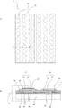
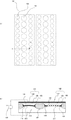
以下に、本発明の実施の形態について図を用いて説明する。図1(a)は、本発明の静電容量型トランスデューサの一実施形態の上面図であり、図1(b)は、図1(a)のA−B断面図である。本実施形態は、第一のセル12と第二のセル19をそれぞれ複数有する静電容量型トランスデューサ1を複数有している。図1では、2つの静電容量型トランスデューサ1のみを記載しているが、トランスデューサ数は幾つでも構わない。また、静電容量型トランスデューサ1は、22個の第一のセル12と8個の第二のセル19から構成されているが、それぞれの個数は幾つであっても構わない。また、セルの配列はどのような配列でも構わない。
Hereinafter, embodiments of the present invention will be described with reference to the drawings. FIG. 1A is a top view of an embodiment of the capacitive transducer of the present invention, and FIG. 1B is a cross-sectional view taken along line AB of FIG. The present embodiment has a plurality of
第一のセル12は、基板2、基板2上に形成される絶縁膜3、絶縁膜3上に形成される第一の電極4、第一の電極4上の絶縁膜5を有する。さらに、第一の電極4と対向する第二の電極6とメンブレン7とを含む振動膜8と、振動膜8を支持する振動膜支持部10、キャビティ(間隙)9とを有している。基板2がガラス基板などの絶縁性基板の場合、絶縁膜3はなくてもよい。第二のセル19は、第一のセル12とほぼ同じ構成である。第二のセル19では、振動膜16の第二のばね定数が第一のセル12の振動膜8の第一のばね定数より低い構成となっている。図1(b)では、振動膜16が振動膜8と同じ材料、厚みで構成されており、振動膜16の直径22を振動膜8の直径21より大きくすることにより、第二のばね定数を小さくしている。ここでは振動膜の形状は円形であるが、正方形、長方形等の形状でも構わない。
The
また、第一のセル12及び第二のセル16の第一の電極と第二の電極との間に電圧を印加する電圧印加手段11を有している。本実施形態では、振動膜8、16のメンブレン7、14は絶縁膜である。特に、窒化シリコン膜は、低い引張り応力、例えば、300MPa以下の引張り応力で形成することが出来るので、窒化シリコン膜の残留応力による振動膜の大きな変形を防止することができ望ましい。ただし、振動膜8、16のメンブレン7、14は絶縁膜でなくとも構わない。例えば、1Ωcm以下の低抵抗シリコン単結晶をメンブレン7、14として用いることも出来る。その場合、メンブレンを第二の電極として用いることも出来る。
Further, voltage application means 11 for applying a voltage between the first electrode and the second electrode of the
上記構成のままで、第一の電極4、13或いは第二の電極6、14に共通の電圧を印加した場合、受信時の振動膜の振動を電気信号に変換する電気機械変換係数、或いは送信時に電気信号を振動膜の振動に変換する電気機械変換係数は、第一のセル12のほうが第二のセル16より低い。なぜなら、第二のセルの振動膜16のばね定数が第一のセル12のばね定数より低い構成となっており、振動膜のばね定数が高いセルのプルイン電圧は、振動膜のばね定数が低いセルのプルイン電圧より高いためである。そこで、本構成では、電圧を印加しない状態で、第一のセルの振動膜にかかる静電引力を、第二のセルの振動膜にかかる静電引力と異なる構成としている。この様にした構成で、電圧印加手段11により共通電極に共通電圧を印加した場合、第一のセルと第二のセルにおいて異なる電位差が生じ、第一のセルの振動膜にかかる静電引力が、第二のセルの振動膜にかかる静電引力より大きくなる。この電位差を、上記ばね定数の違いによるプルイン電圧の差の分を打ち消す値にしておけば、両方のセルがほぼ同じ印加電圧でプルインするようになる。また、第一のセルと第二のセルが有するプルイン電圧に対する印加電圧の比率を、ほぼ同じにすることも出来る。この為には、上記ばね定数の違いによるプルイン電圧差が存在する構成における第一のセルのプルイン電圧に対する印加電圧の比率と第二のセルのプルイン電圧に対する印加電圧の比率との差の分の電位差を、例えば一方のセルに与えておけばよい。
With the above configuration, when a common voltage is applied to the
こうした構成にする方法は、どのような方法であっても構わない。上記ばね定数の違いにより、例えば、第一のセルと第二のセルのプルイン電圧の差が20Vあったとする。この時、第二のセルのメンブレン14を20V分帯電させる(図1(b)参照)。この状態で、第一の電極4に第一のセルがプルインする正符号の電圧を印加すると、第一のセルでは第一の電極4に印加した電圧分だけ電位差が生じる。一方、第二のセルでは、第一の電極13に印加した電圧と上記帯電による電位20Vの差の分だけ電位差が生じる。これにより、共通電極である第一の電極4、13に印加した共通電圧で、ばね定数の異なるセル12、19を同時にプルインさせることが出来る。また、もう一方の共通電極である第二の電極6、15に共通電圧を印加してもよい。第二の電極6、15には、第一のセル12がプルインする負の符号の電圧を印加すればよい。さらに、第二のセル19のメンブレン14の帯電は、−20Vでもよい。その場合には、共通電極である第一の電極4、13に印加する共通電圧の符号を、負にして印加すればよい。また、共通電極である第二の電極6、15に共通電圧を印加する場合には、正の符号にして印加すればよい。第一のセルのプルイン電圧と上記帯電による電圧との差が、第二のセルのプルイン電圧となるように、共通電極に共通電圧を印加すればよい。
Any method may be used for such a configuration. For example, it is assumed that the difference in pull-in voltage between the first cell and the second cell is 20 V due to the difference in the spring constant. At this time, the membrane 14 of the second cell is charged by 20 V (see FIG. 1B). In this state, when a positive sign voltage that pulls in the first cell is applied to the
さらに、第一のセル12を帯電させてもよい。その場合、例えば、第一のセルのメンブレン7を−20V分帯電させる。この状態で、第一の電極4、13に第二のセル19がプルインする正の電圧を印加すると、第二のセルでは第一の電極4、13に印加した電圧分だけ電位差が生じる。一方、第一のセル12では、第一の電極4に印加した電圧と上記帯電による電位の差の分だけ電位差が生じる。これにより、共通電極である第一の電極4、13に印加した共通電圧で、ばね定数の異なるセル12、19を同時にプルインさせることが出来る。また、もう一方の共通電極である第二の電極6、15に共通電圧を印加してもよい。第二の電極6、15には、第二のセル19がプルインする負の符号の電圧を印加すればよい。さらに、第一のセル12のメンブレン7の帯電は、20Vでもよい。その場合には、共通電極である第一の電極4、13に印加する共通電圧の符号を、負の符号にして印加すればよい。また、共通電極である第二の電極6、15に共通電圧を印加する場合には、正の符号にして印加すればよい。第二のセルのプルイン電圧と上記帯電による電圧との差が、第一のセルのプルイン電圧となるように、共通電極に共通電圧を印加すればよい。
Further, the
本構成の帯電個所は、メンブレン7、14だけではなく、絶縁膜5、13であってもよい。つまり、第一のセルと第二のセルの少なくとも一方に、少なくとも一部が帯電した絶縁部が配置されているようにすればよい。上記構成では、上記ばね定数の違いによる第一のセルと第二のセルのプルイン電圧の差の分だけ、どちらか一方のセルの一部を帯電させる。次に、帯電させていないセルのプルイン電圧と上記帯電による電圧との電位差が、帯電させているセルのプルイン電圧となるように、共通電極に共通電圧を印加すればよい。本構成により、第一のセルのプルイン電圧と第二のセルのプルイン電圧との差を少なくしたり、或いは同じにしたりすることが出来るので、送信感度或いは受信感度を向上することが出来る。また上記では、プルイン電圧の差について述べたが、プルイン電圧に対する印加電圧の比率の差の場合でも共通のことが言える。以上より、本実施形態の静電容量型トランスデューサでは、受信時の周波数帯域或いは送信時の周波数帯域を広くすることが出来るとともに、送信感度或いは受信感度を向上することが出来る。
The charging location of this configuration may be not only the membranes 7 and 14 but also the insulating
さらに、第一のセル12の振動膜の面積は、第二のセル19の振動膜の面積より小さく、かつ、第一のセルの振動膜厚さは、第二のセルの振動膜厚さと同じとすることも出来る。本構成にすることによって、振動膜のばね定数が高いセルと振動膜のばね定数が低いセルとを同じ作製プロセスによって作製出来る。従って、低いコストで静電容量型トランスデューサを作製することが出来る。また、本構成にすることによって、第一のセルの振動膜と第二のセルの振動膜とを同じ作製工程によって作製することが出来る。第一のセルの振動膜厚さと、第二のセルの振動膜厚さを同じでなく、どちらかの振動膜をエッチングしたり、或いは異なる工程で成膜したりした場合、第一のセルの振動膜のばね定数と第二のセルの振動膜のばね定数との比がばらつきやすい。この様な場合、静電容量型トランスデューサの送信或いは受信感度や周波数帯域の帯域が所望のものとならないことがある。従って、上記構成により、送信感度或いは受信感度や周波数帯域のばらつきを小さく出来る。
Furthermore, the area of the diaphragm of the
さらに、図3(b)に示すように、第一のセルの振動膜厚さは、第二のセルの振動膜厚さより厚く、かつ、第一のセルの振動膜面積は、第二のセルの振動膜面積と同じである構成とすることも出来る。本構成にすることによって、図3(a)にように、上面から見た各セルの形状が同じにでき、全てのセルの放射インピーダンスを揃えることが出来る。従って、各セルの放射インピーダンスが同じであるため、各セルの振動膜は同じ態様の振動をするので、電気機械変換係数を低下させるような不要な振動を防止することが出来る。 Further, as shown in FIG. 3B, the vibration film thickness of the first cell is larger than the vibration film thickness of the second cell, and the vibration film area of the first cell is the second cell. It can also be set as the structure which is the same as the vibration membrane area. By adopting this configuration, as shown in FIG. 3A, the shape of each cell viewed from above can be made the same, and the radiation impedances of all the cells can be made uniform. Therefore, since the radiation impedance of each cell is the same, the vibrating membranes of each cell vibrate in the same manner, so that unnecessary vibration that reduces the electromechanical conversion coefficient can be prevented.
上記構成は、ばね定数の異なるセルが3種類以上存在する場合にも適用出来る。例えば図2(b)のように、ばね定数の異なるセル毎に、絶縁層の一部を異なる態様で帯電させたり或いは非帯電にしたりすればよい。基準となるセルを決め、ばね定数の違いによるプルルイン電圧の差の分だけ、各セルの一部を帯電させたり或いは非帯電にしたりする。帯電させる部分は、各セルでメンブレンを帯電させてもよいし、セル毎に絶縁膜5、23を帯電させてもよい。基準となるセルのプルイン電圧と上記帯電による電圧との電位差が、帯電させているセルのプルイン電圧となるように、共通電極に共通電圧を印加すればよい。
The above configuration can also be applied when there are three or more types of cells having different spring constants. For example, as shown in FIG. 2B, a part of the insulating layer may be charged in a different manner or uncharged for each cell having a different spring constant. A reference cell is determined, and a part of each cell is charged or uncharged by the difference in the pull-in voltage due to the difference in spring constant. In the portion to be charged, the membrane may be charged in each cell, or the insulating
上記構成では、さらに、ばね定数の異なるセル毎に、異なる態様でセルの一部を帯電させたり非帯電にしたりすることにより、共通電極に共通電圧を印加せずに別個の電圧で駆動することも可能である。以上の構成により、ばね定数の異なる各セルのプルイン電圧の差を少なくしたり、或いは同じにしたりすることが出来る。また、ばね定数の異なる各セルのプルイン電圧に対する印加電圧の比率の差を少なくしたり、或いは同じにしたりすることが出来るので、送信感度或いは受信感度を向上することが出来る。 In the above configuration, each cell having a different spring constant is driven by a separate voltage without applying a common voltage to the common electrode by charging or uncharging a part of the cell in a different manner. Is also possible. With the above configuration, the difference in pull-in voltage between cells having different spring constants can be reduced or the same. Further, since the difference in the ratio of the applied voltage to the pull-in voltage of each cell having a different spring constant can be reduced or made the same, the transmission sensitivity or the reception sensitivity can be improved.
上記構成において、セルを帯電させる方法はどのような方法であっても構わない。例えば、静電容量型トランスデューサの製造途中で帯電させることも出来るし、製造後や使用前、更には使用中にセルを帯電させることも出来る。静電容量型トランスデューサの製造途中で帯電させる場合には、セルの帯電させたい箇所(メンブレンや絶縁膜)にコロナ放電処理を施し、帯電させればよい。また、製造後や使用中に帯電させる場合には、帯電させたいセルをプルインさせて、メンブレンや絶縁膜を帯電させればよい。 In the above configuration, any method may be used for charging the cell. For example, the electrostatic capacity transducer can be charged during the manufacturing process, or the cell can be charged after the manufacturing process, before the use, or even during the use. In the case of charging during the production of the capacitance type transducer, it is only necessary to charge the portion (membrane or insulating film) to be charged of the cell by performing corona discharge treatment. In addition, when charging is performed after manufacturing or during use, a cell or an insulating film may be charged by pulling in a cell to be charged.
上記構成において、帯電箇所は、帯電しやすい材料で構成されていれば、どのような材料の部分であっても構わない。例えば、シリコン酸化膜、窒化シリコン膜、チタン酸バリウム、チタン酸ストロンチウム、チタン酸バリウム・ストロンチウム、五酸化タンタル、酸化ニオブ安定化五酸化タンタル、酸化アルミニウム、酸化チタンなどが挙げられる。また、振動膜等の1種類の膜を単層にするだけでなく、複数種類の膜を複数層組み合わせて構成したりしてもよい。例えば、図3に示すように、セルのメンブレンを二層構造とし、窒化シリコン膜とシリコン酸化膜などで構成したりしてもよい。これらの材質、組成比などにより帯電量を調整することが出来る。 In the above configuration, the charged portion may be a portion of any material as long as it is made of a material that is easily charged. For example, a silicon oxide film, a silicon nitride film, barium titanate, strontium titanate, barium / strontium titanate, tantalum pentoxide, niobium oxide stabilized tantalum pentoxide, aluminum oxide, titanium oxide, and the like can be given. Further, not only a single type of film such as a vibrating membrane may be a single layer, but a plurality of types of films may be combined to form a plurality of layers. For example, as shown in FIG. 3, the cell membrane may have a two-layer structure, and may be composed of a silicon nitride film and a silicon oxide film. The charge amount can be adjusted by these materials and composition ratios.
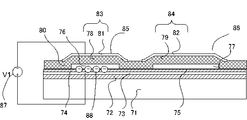
ここで、図4を用いて、本発明の作製方法の一実施形態を説明する。図4は、静電容量型トランスデューサの断面図であり、図1とほぼ同様の構成である。図4は、図1(a)のA−B断面相当図である。まず、図4(a)に示すように、基板71上に絶縁膜72を形成する。基板71はシリコン基板であり、絶縁膜72は第一の電極との絶縁を形成するためのものである。基板71がガラス基板のような絶縁性基板の場合、絶縁膜72は形成しなくともよい。また、基板71は、表面粗さの小さな基板が望ましい。表面粗さが大きい場合、本工程の後工程での成膜工程でも、表面粗さが転写されていって、表面粗さにより第一の電極と第二の電極間の距離が各セル間でばらついてしまう。このばらつきは、電気機械変換係数のばらつきとなるため、感度や帯域のばらつきとなる。従って、基板71は、表面粗さの小さな基板が望ましい。
Here, an embodiment of the manufacturing method of the present invention will be described with reference to FIGS. FIG. 4 is a cross-sectional view of the capacitive transducer, and has substantially the same configuration as FIG. FIG. 4 is a cross-sectional view corresponding to the line AB in FIG. First, as shown in FIG. 4A, the insulating
さらに、第一の電極73を形成する。第一の電極73は、表面粗さが小さい導電材料が望ましく、例えば、チタン、アルミニウム等である。基板と同様に、第一の電極の表面粗さが大きい場合、表面粗さにより第一の電極と第二の電極間の距離が、各セル間、複数のセルを有する各エレメント間でばらついてしまうため、表面粗さが小さい導電材料が望ましい。
Further, the
次に、絶縁膜74、75を形成する。絶縁膜74、75は、表面粗さが小さい絶縁材料が望ましく、第一の電極と第二の電極との間に電圧が印加された場合の第一の電極と第二の電極間の電気的短絡、或いは絶縁破壊を防止するために形成する。低電圧で駆動する場合は、メンブレンが絶縁体であるため、絶縁膜74、75を形成しなくともよい。こうした絶縁膜は、さらに、本工程の後工程で実施する犠牲層除去時に第一の電極がエッチングされることを防止するために形成する。犠牲層除去時のエッチング液やエッチングガスにより、第一の電極がエッチングされない場合は、絶縁膜74、75を形成しなくともよい。基板と同様に、絶縁膜74、75の表面粗さが大きい場合、表面粗さにより第一の電極と第二の電極間の距離が各セル間でばらついてしまうため、表面粗さが小さい絶縁膜が望ましい。例えば、窒化シリコン膜、シリコン酸化膜等である。
Next, insulating
次に、図4(b)に示すように、犠牲層76、77を形成する。犠牲層76の幅は、犠牲層77の幅より小さくなるように形成している。本構成にすることによって、第一のセルのキャビティの直径を第二のセルのキャビティの直径より小さくすることが出来る。犠牲層76、77は、表面粗さが小さい材料が望ましい。基板と同様に、犠牲層の表面粗さが大きい場合、表面粗さにより第一の電極と第二の電極間の距離が各セル間でばらついてしまうため、表面粗さが小さい犠牲層が望ましい。また、犠牲層を除去するエッチングの時間を短くするために、エッチング速度の速い材料が望ましい。また、犠牲層を除去するエッチング液やエッチングガスに対して、絶縁膜やメンブレンがほぼエッチングされないような犠牲層材料が求められる。犠牲層を除去するエッチング液やエッチングガスに対して、絶縁膜やメンブレンがエッチングされる場合、振動膜の厚さがばらつき、第一の電極と第二の電極との間の距離のばらつきが発生することがある。振動膜の厚さばらつき、第一の電極と第二の電極との間の距離ばらつきは、各セル間の感度や帯域のばらつきとなる。絶縁膜やメンブレンが窒化シリコン膜或いはシリコン酸化膜の場合、表面粗さが小さく、絶縁膜やメンブレンがエッチングされにくいエッチング液或いはエッチングガスを用いることが出来る犠牲層材料が望ましい。例えば、アモルファスシリコン、ポリイミド、クロム等である。特に、クロムのエッチング液は、窒化シリコン膜或いはシリコン酸化膜をほぼエッチングしないので、絶縁膜やメンブレンが窒化シリコン膜或いはシリコン酸化膜であるのが望ましい。
Next, as shown in FIG. 4B,
次に、図4(c)に示すように、メンブレン78、79を形成する。メンブレン78、79は、低い引張り応力が望ましい。例えば、300MPa以下の引張り応力がよい。窒化シリコン膜は応力コントロールが可能であり、300MPa以下の低い引張り応力にすることが出来る。メンブレンが圧縮応力を有する場合、メンブレンがスティッキング或いは座屈を引き起こし、大きく変形することがある。また、大きな引張り応力の場合、第一のメンブレンが破壊されることがある。従って、メンブレン78、79は、低い引張り応力が望ましい。例えば、応力コントロールが可能で、低い引張り応力に出来る窒化シリコン膜が望ましい。
Next,
さらに、図示しないエッチングホールを形成し、エッチングホールを介して、犠牲層76、77を除去して、エッチングホールを封止する。これにより、間隙76、77が形成される。例えば、窒化シリコン膜や酸化シリコン膜で封止することが出来る。犠牲層除去工程或いは封止工程は、第二の電極の形成後に行うことも出来る。
Further, an etching hole (not shown) is formed, the
次に、図4(d)に示すように、第二の電極81、82を形成する。第二の電極81、82は、残留応力が小さい材料が望ましく、アルミニウムなどである。犠牲層除去工程或いは封止工程を第二の電極形成後に行う場合、第二の電極は、犠牲層エッチングに対するエッチング耐性や耐熱性を有する材料が望ましい。例えば、チタンなどである。図4(d)では、第二の電極81、82は、電気的に分離されているが、電気的に繋がっていてもよい。これにより、振動膜支持部80で支持された振動膜83、84が形成される。
Next, as shown in FIG. 4D,
次に、図4(e)に示すように、第二のセル86のメンブレン79を帯電させる。図4(d)の状態では、まだ第二のセルは帯電していない為、共通電極に共通電圧を印加した場合、2種類のセルを同じ電圧でプルインさせることが出来ない。また、2種類のセルについて、共通電圧で、各プルイン電圧に対する印加電圧の比率を同じ状態にして駆動することができない。従って、外部の電圧印加手段87により、第二のセル86がプルインする電圧を第一の電極と第二の電極間に印加すると、第二のセル86よりも第一のセル85のばね定数が高い為、第二のセルだけがプルインする。このことを利用して第二のセルのみをプルインさせる。第二のセルがプルインすると、絶縁膜に電荷が注入され、絶縁膜が帯電する。図4(e)のセルの場合、メンブレン79を形成する窒化シリコン膜に電荷88が溜まる。帯電させる符号の方向は、のちに共通電極に共通電圧を印加した時に、第二のセル86にかかる電界の強度が、第一のセル85にかかる電界の強度と同等の強度となる符号方向に帯電させる。この帯電量は、プルインさせる電圧印加の時間などで制御することが出来る。
Next, as shown in FIG. 4E, the
図4(e)において、絶縁膜の種類や膜構成を変えて、絶縁膜74などを帯電させることも出来る。また、図4(a)の後に、図5に示す工程を実施して、セルを帯電させることも出来る。図5では、絶縁膜74をコロナ放電で帯電させている。例えば、ワイヤ状の電極91を、帯電させたい部分の上部に配置する。電極91は、高電圧を印加出来る接地(93で示す)された電源92と接続されている。第一の電極73を接地(94で示す)し、電極91に数kVの高電圧を印加して、帯電させたい箇所にコロナ放電をする。こうすると、電極91からはマイナス電荷が放電されるため、シリコン酸化膜の表面側にはマイナス電荷95が、第一の電極73側の表面にはプラス電荷が帯電する。図5において、電源92の電位の向きを逆にすれば、シリコン酸化膜の表面側をプラス電荷で帯電させることが出来る。帯電させたい箇所に電極91を移動させ、コロナ放電を行うことで、所望の箇所に所望の電荷を帯電させることが出来る。帯電量は、コロナ放電のための印加電圧の大きさなどで制御することが出来る。
In FIG. 4E, the insulating
図6の様に、ばね定数の高い第一のセル85を帯電させる場合、帯電させる符号方向は、のちに共通電極に共通電圧を印加した時に、第二のセルにかかる電界の強度が第一のセルにかかる電界の強度と同等となる方向に帯電させる。帯電した電荷88を安定化させる為に、加熱処理を施してもよい。例えば、大気中で150℃、1時間程度の処理を行うと、帯電した電荷が安定する。
As shown in FIG. 6, when the
以上では、共通電極に共通電圧を印加した場合に、ばね定数の異なるセルのプルインが同時に生じるように帯電させた。また、ばね定数の異なるセルが有するプルイン電圧に対する印加電圧の比率を、各セルで同じにするように帯電させることも出来る。共通電極に共通電圧を印加した場合に各セルでプルイン電圧に対する印加電圧の比率が同じになるように、各セルを帯電させることで、各セルの電気機械変換係数を高くすることが出来る。 As described above, when a common voltage is applied to the common electrode, the cells are charged so that pull-ins of cells having different spring constants are generated simultaneously. In addition, the cells can be charged so that the ratio of the applied voltage to the pull-in voltage of cells having different spring constants is the same in each cell. By charging each cell so that the ratio of the applied voltage to the pull-in voltage is the same in each cell when a common voltage is applied to the common electrode, the electromechanical conversion coefficient of each cell can be increased.
上記作製方法で静電容量型トランスデューサを作製することにより、受信時の周波数帯域或いは送信時の周波数帯域を広くすることが出来るとともに、送信感度或いは受信感度を向上させられる静電容量型トランスデューサを作製出来る。 By producing a capacitive transducer by the above production method, it is possible to widen the frequency band at the time of reception or the frequency band at the time of transmission, and to produce a capacitive transducer that can improve transmission sensitivity or reception sensitivity. I can do it.
以下、より具体的な実施例を挙げて本発明を詳細に説明する。
(実施例1)
本発明の実施例1について図1を用いて説明する。本実施例の基本構造は上記実施形態と同じである。第一のセル12は、300μm厚さのシリコン基板2、シリコン基板2上の絶縁膜3、絶縁膜3上の第一の電極4、第一の電極4上の絶縁膜5を有する。さらに、第二の電極6とメンブレン7とを含む振動膜8と、振動膜8を支持する振動膜支持部10、キャビティ(間隙)9を有している。キャビティ9の高さは100nmである。さらに、第一の電極と第二の電極との間に電圧を印加する電圧印加手段11を有している。
Hereinafter, the present invention will be described in detail with reference to more specific examples.
Example 1
A first embodiment of the present invention will be described with reference to FIG. The basic structure of this example is the same as that of the above embodiment. The
絶縁膜3は、熱酸化により形成した厚さ1μmのシリコン酸化膜である。絶縁膜5は、Prasma−Enhanced−Chemical−Vapor Deposition(PE−CVD)により形成した100nmのシリコン酸化膜である。第一の電極4は厚さが50nmのチタンであり、第二の電極6は厚さが100nmのアルミニウムである。メンブレン7はPE−CVDにより作製した窒化シリコン膜であり、200MPa以下の引張り応力で形成し、厚みは1400nmである。
The insulating
本実施例の静電容量型トランスデューサは、図示しない引き出し配線を用いることで、第二の電極6、15から電気信号を引き出すことが出来る。静電容量型トランスデューサで超音波を受信する場合、直流電圧を第一の電極4、13に印加しておく。超音波を受信すると、第二の電極6、15とメンブレン7、14をそれぞれ有する振動膜8、16が変形するため、第二の電極6、15と第一の電極4、13との間のキャビティ9、17の距離が変わり、静電容量が変化する。この静電容量変化によって、引き出し配線に電流が流れる。この電流を図示しない電流−電圧変換素子によって電圧として、超音波を受信することが出来る。また、第一の電極に直流電圧を印加し、交流電圧を第二の電極に印加し、静電気力によって、振動膜8、16を振動させることが出来る。これによって、超音波を送信することが出来る。
The capacitive transducer according to the present embodiment can extract an electrical signal from the second electrodes 6 and 15 by using a lead wiring (not shown). When receiving ultrasonic waves with a capacitive transducer, a DC voltage is applied to the
第二のセル19は、第一のセル12とほぼ同じ構成である。第一のセル12では、振動膜8の直径21が36μmである一方、第二のセル19では、振動膜16の直径22が44μmである。そのため、振動膜16のばね定数がセル12のばね定数より低い構成となっている。また、第二のセル19のキャビティ17の高さも100nmである。図1(b)では、振動膜16が振動膜8と同じ材料、厚みで構成されており、振動膜16の直径を振動膜8より大きくすることにより、ばね定数を小さくしている。第一のセルのばね定数が82kN/mであり、第二のセルのばね定数が55kN/mである。ここでのばね定数とは、振動膜にかかる荷重を、そのときの振動膜の平均変位で割った値のことである。ばね定数が高い振動膜を有する第一のセルと、ばね定数が低い振動膜を有する第二のセルとを有しているため、受信時の周波数帯域或いは送信時の周波数帯域を広くすることが出来る。
The second cell 19 has substantially the same configuration as the
また、本実施例では、振動膜16が振動膜8と同じ材料、厚みで構成されており、振動膜を形成する工程は、第一のセルと第二のセルとで同じにすることが出来る。従って、第一のセルの振動膜のばね定数と第二のセルの振動膜のばね定数との比率のばらつきを低減出来るため、送信感度或いは受信感度や周波数帯域のばらつきを小さく出来る。 Further, in this embodiment, the vibration film 16 is made of the same material and thickness as the vibration film 8, and the process of forming the vibration film can be the same in the first cell and the second cell. . Accordingly, since the variation in the ratio between the spring constant of the diaphragm of the first cell and the spring constant of the diaphragm of the second cell can be reduced, the variation in transmission sensitivity, reception sensitivity, and frequency band can be reduced.
また、本構成では、振動膜16が振動膜8と同じ材料、厚みで構成されているとともに、絶縁膜5、23の厚さもほぼ同じ100nmであるため、第一の電極と第二の電極との距離はほぼ同じになる。さらに、上述した様に、第二のセル19の振動膜16のばね定数が第一のセル12の振動膜8のばね定数より低い構成となっている。振動膜の復元力より静電引力のほうが大きくなる電圧がプルイン電圧であるので、ばね定数の違いによる第一のセルのプルイン電圧は第二のセルのプルイン電圧より高くなる。ここでは、第一のセル12のプルイン電圧は155Vであり、第二のセル19のプルイン電圧は100Vである。
Further, in this configuration, the vibration film 16 is made of the same material and thickness as the vibration film 8, and the thicknesses of the insulating
本実施例では、共通電極に印加する共通電圧は125Vである。つまり、第一のセルの上記プルイン電圧の80%の電圧である。このままの状態で共通電極に125Vを印加すると、第二のセルにも125Vの電位差が生じる為、第二のセルはプルインする。セルがプルインすると、振動膜が振動し難くなり、電気機械変換係数が大きく低下する。その為、セルに印加する電圧は、プルイン電圧よりも低く、なるべくプルイン電圧に近い値とすることが望ましい。本実施例では、第一のセルと第二のセルを、各セルのプルイン電圧の80%で駆動出来るようにする。その場合、上記構成のままでは、第一のセルに生じさせる電位差は125V、第二のセルに生じさせる電位差は80Vである。ここで第一のセルと第二のセルに生じさせる電位差には、45Vの違いがあるため、第二のセルを45V分帯電させる処理を施す。本実施例では、第二のセルのみをプルインさせて、第二のセルのメンブレン14を45V分帯電させる。外部の電圧印加手段11から、共通電極である第二の電極6、15に150Vの電圧を印加し、第二のセル19のみをプルインさせる。この状態を1時間保持した後に、共通電圧を0Vに戻すと、第二のセルが有するメンブレン14には、約45V分のマイナス電荷が帯電する。 In this embodiment, the common voltage applied to the common electrode is 125V. That is, the voltage is 80% of the pull-in voltage of the first cell. If 125 V is applied to the common electrode in this state, a potential difference of 125 V is also generated in the second cell, so that the second cell is pulled in. When the cell is pulled in, the vibrating membrane is difficult to vibrate, and the electromechanical conversion coefficient is greatly reduced. Therefore, the voltage applied to the cell is preferably lower than the pull-in voltage and as close to the pull-in voltage as possible. In this embodiment, the first cell and the second cell can be driven at 80% of the pull-in voltage of each cell. In that case, with the above configuration, the potential difference generated in the first cell is 125V, and the potential difference generated in the second cell is 80V. Here, since the potential difference generated between the first cell and the second cell has a difference of 45V, the second cell is charged by 45V. In this embodiment, only the second cell is pulled in, and the membrane 14 of the second cell is charged by 45V. A voltage of 150 V is applied from the external voltage application means 11 to the second electrodes 6 and 15 which are common electrodes, and only the second cell 19 is pulled in. When the common voltage is returned to 0 V after holding this state for 1 hour, the negative charge of about 45 V is charged on the membrane 14 of the second cell.
この状態で、共通電極である第一の電極4、13に−125Vを印加すると、第一のセルでは125Vの電位差が生じ、第二のセルでは80Vの電位差が生じる。これにより、ばね定数の異なるセルの共通電極に共通電圧を印加した場合でも、プルイン電圧に対して同じ印加電圧の比率で駆動することが出来る。プルイン電圧に対する印加電圧の比率に依存する電気機械変換係数は、第一のセルと第二のセルにおいて同じにすることが出来る。
In this state, when −125 V is applied to the
本実施例でも、受信時の周波数帯域或いは送信時の周波数帯域を広くすることが出来るとともに、送信感度或いは受信感度を向上することが出来る。さらに、使用中に再度プルインをさせて帯電処理を行うなど、適宜繰り返し帯電を行いながら使用することが出来る。 Also in this embodiment, the frequency band at the time of reception or the frequency band at the time of transmission can be widened, and the transmission sensitivity or the reception sensitivity can be improved. Furthermore, it can be used while being repeatedly charged as appropriate, for example, by pulling in again during use and performing a charging treatment.
(実施例2)
実施例2の静電容量型トランスデューサの構成を図2を用いて説明する。図2(a)は、本実施例の静電容量型トランスデューサの上面図であり、図2(b)は、図2(a)のA−B断面図である。実施例2の静電容量型トランスデューサ31の構成は、実施例1とほぼ同様である。異なる点は、第一の電極36の上の絶縁膜が、二層構成である点と、ばね定数の異なるセルを3種類有し、それぞれの帯電状態が異なる点である。ばね定数の高い順に、第一のセル32、第二のセル33、第三のセル54と呼ぶ。
(Example 2)
The configuration of the capacitive transducer according to the second embodiment will be described with reference to FIG. FIG. 2A is a top view of the capacitive transducer of this embodiment, and FIG. 2B is a cross-sectional view taken along the line AB of FIG. The configuration of the capacitive transducer 31 of the second embodiment is almost the same as that of the first embodiment. The difference is that the insulating film on the first electrode 36 has a two-layer structure, and there are three types of cells having different spring constants, and the respective charged states are different. They are called the first cell 32, the
第一のセル32の振動膜49の直径は32μm、第二のセル33の振動膜50の直径は40μm、第三のセル54の振動膜51の直径は50μmである。振動膜49、50、51の厚さは全て同じ1400nmである。キャビティ(間隙)39、40、41の高さは全て同じ100nmである。絶縁膜35、37、55は窒化シリコン膜であり、厚さは70nmである。絶縁膜38は酸化シリコン膜であり、厚さは60nmである。絶縁膜37、53、55は、上記実施形態において図4(a)で述べた方法と同様の方法により、窒化シリコン膜で形成出来る。絶縁膜38も上記実施形態において図4(a)で述べた方法と同様の方法により、絶縁膜35、37、55を作成した後に、酸化シリコン膜で形成出来る。
The diameter of the diaphragm 49 of the first cell 32 is 32 μm, the diameter of the diaphragm 50 of the
本構成にすることにより、第一のセルのばね定数は103kN/m、第二のセルのばね定数は66kN/m、第三のセルのばね定数は42kN/mとなる。また、このままの構成における各セルのプルイン電圧は、第一のセルは200V、第二のセルは125V、第三のセルは75Vとなる。本実施例における静電型トランスデューサの駆動電圧は、各セルのプルイン電圧に対して80%の印加電圧とする。この場合、各セルの駆動電圧は、第一のセルは160Vであり、第二のセルは100V、第三のセルは60Vとなる。共通電極に印加する共通電圧を100Vとすると、各セルの上記駆動電圧との差分は、第一のセルは60V、第二のセルは0V、第三のセルは−40Vとなる。この共通電圧との差分を、各セルにおいて帯電させる。 With this configuration, the spring constant of the first cell is 103 kN / m, the spring constant of the second cell is 66 kN / m, and the spring constant of the third cell is 42 kN / m. Further, the pull-in voltage of each cell in the configuration as it is is 200V for the first cell, 125V for the second cell, and 75V for the third cell. The driving voltage of the electrostatic transducer in this embodiment is an applied voltage of 80% with respect to the pull-in voltage of each cell. In this case, the driving voltage of each cell is 160V for the first cell, 100V for the second cell, and 60V for the third cell. Assuming that the common voltage applied to the common electrode is 100V, the difference from the drive voltage of each cell is 60V for the first cell, 0V for the second cell, and -40V for the third cell. The difference from the common voltage is charged in each cell.
本実施例での帯電方法は、コロナ放電処理を施す事とする。まず、図4(a)と同様の方法で、基板34上の絶縁膜57に形成された第一の電極36上に、絶縁膜35、37、55を成膜する。そして、図5と同様にして、各セルのキャビティの内側となる部分の絶縁膜を帯電させる。第一のセルのキャビティ内側の部分の絶縁膜は、−60Vに帯電させる。第三のセルのキャビティ内側の部分の絶縁膜は、40Vに帯電させる。第一のセルと第三のセルの絶縁膜を帯電(52、53で示す)させた後、大気中で150℃、1時間程度加熱すると、帯電状態が安定化する。その後、二層目の絶縁膜38を成膜する。成膜後の工程は、図4(b)〜図4(d)と同様の工程を経る事で、図2に記載の静電型トランスデューサを作成することが出来る。なお、図2において、42、43〜45は、それぞれ、振動膜支持部、メンブレンである。
The charging method in this embodiment is performed by corona discharge treatment. First, insulating
この状態で、電圧印加手段56により、共通電極である第二の電極46、47、48に100Vを印加すると、第一のセルでは160Vの電位差が生じ、第二のセルでは100Vの電位差が生じ、第三のセルでは60Vの電位差が生じる。これにより、ばね定数の異なるセルの共通電極に共通電圧を印加した場合でも、プルイン電圧に対して同じ比率の印加電圧で駆動することが出来る。このプルイン電圧に対する印加電圧の比率に依存する電気機械変換係数は、第一のセルと第二のセルと第三のセルにおいて同じにすることが出来る。従って、本実施例の静電容量型トランスデューサでも、受信時の周波数帯域或いは送信時の周波数帯域を広くすることが出来るとともに、送信感度或いは受信感度を向上することが出来る。 In this state, when 100 V is applied to the second electrodes 46, 47, and 48, which are common electrodes, by the voltage application means 56, a potential difference of 160 V is generated in the first cell, and a potential difference of 100 V is generated in the second cell. In the third cell, a potential difference of 60 V is generated. Thereby, even when a common voltage is applied to the common electrode of cells having different spring constants, it can be driven with an applied voltage having the same ratio as the pull-in voltage. The electromechanical conversion coefficient depending on the ratio of the applied voltage to the pull-in voltage can be the same in the first cell, the second cell, and the third cell. Therefore, the capacitive transducer of the present embodiment can widen the frequency band at the time of reception or the frequency band at the time of transmission, and can improve the transmission sensitivity or the reception sensitivity.
(実施例3)
実施例3の静電容量型トランスデューサの構成を図3を用いて説明する。実施例3の静電容量型トランスデューサ61の構成は、実施例1とほぼ同様であり、図3(b)は、図3(a)のA−B断面図である。本実施例では、振動膜のばね定数が高いセルの振動膜厚さは、振動膜のばね定数が低いセルの振動膜厚さより厚く、かつ、振動膜のばね定数が高いセルの振動膜面積は、振動膜のばね定数が低いセルの振動膜面積と同じである。
(Example 3)
The configuration of the capacitive transducer according to the third embodiment will be described with reference to FIG. The configuration of the capacitive transducer 61 of the third embodiment is substantially the same as that of the first embodiment, and FIG. 3B is a cross-sectional view taken along the line AB of FIG. In this example, the vibration film thickness of the cell having a high vibration film spring constant is larger than the vibration film thickness of the cell having a low vibration film spring constant, and the vibration film area of the cell having a high vibration film spring constant is The area of the diaphragm of the cell having the low spring constant of the diaphragm is the same.
第一のセル62の振動膜77の直径及び第二のセル63の振動膜78の直径は、ともに36μmであり、振動膜厚さがそれぞれ1400nmと1200nmである。本構成にすることにより、第一のセルのばね定数が82kN/m、第二のセルのばね定数が55kN/mとなる。キャビティ70、71の高さは100nmである。絶縁膜68、69は窒化シリコン膜であり、厚さは175nmである。絶縁膜68、69は、上記実施形態において図4(a)で述べたのと同様の方法により、窒化シリコン膜で作成出来る。本実施例の静電容量型トランスデューサは、ばね定数が高い振動膜を有する第一のセル62と、ばね定数が低い振動膜を有する第二のセル63とを有しているため、受信時の周波数帯域或いは送信時の周波数帯域を広くすることが出来る。
The diameter of the
本構成では、第二のセル63の振動膜78のばね定数が第一のセル62の振動膜77のばね定数より低い構成となっている。振動膜の復元力より静電引力のほうが大きくなる電圧がプルイン電圧であるので、このままの構成における第一のセルのプルイン電圧は、第二のセルのプルイン電圧より高くなる。第一のセル62のプルイン電圧は155Vであり、第二のセル63のプルイン電圧は90Vである。本実施例における静電型トランスデューサの駆動電圧を、各セルのプルイン電圧の80%になるようにする場合を考える。この場合、このままの構成における各セルの駆動電圧は、第一のセルは125V、第二のセルは72Vとなる。共通電極に印加する共通電圧を125Vとすると、各セルの駆動電圧との差分は、±53Vとなる。この共通電圧との差分を、第二のセル63を帯電させることで補償する。
In this configuration, the spring constant of the
本実施例での帯電方法についても、コロナ放電処理を施す事とする。まず、図4(a)と同様の方法で、基板64上の絶縁膜65に形成された第一の電極66上に、絶縁膜68、69を成膜する。そして、図5と同様にして、第二のセルのキャビティ71の内側となる部分の絶縁膜69を、−53V分帯電(67で示す)させる。次に大気中で150℃、1時間程度加熱すると、帯電状態が安定化する。その後、図4(b)〜図4(d)の工程と同様の工程を経る。
The charging method in this embodiment is also subjected to corona discharge treatment. First, insulating films 68 and 69 are formed on the first electrode 66 formed on the insulating film 65 on the substrate 64 by the same method as in FIG. Then, in the same manner as in FIG. 5, the insulating film 69 in the portion inside the
本構成を作製するために第一のセル62の第二の電極74及び第二のセル63の第二の電極75を形成した後に、第一のセル62の振動膜77の厚さを厚くするために、第二の電極74の下のメンブレンと同じ材料である窒化シリコンを成膜してメンブレン72を形成する。その後、第二のセル63の第二の電極75上にも積層された窒化シリコンをエッチングにより除去する。その際、第二のセル63の第二の電極75がエッチングストップ層となるため、本構成のように、第一のセル62の第二の電極74と第一の電極66の距離を、第二のセル63の第二の電極75と第一の電極66の距離と容易に同じにすることが出来る。
After forming the
この状態で、電圧印加手段79により、図示しない個所で電気的に導通している共通電極である第二の電極74、75に125Vを印加すると、第一のセルでは125Vの電位差が生じ、第二のセルでは72Vの電位差が生じる。これにより、ばね定数の異なるセルの共通電極に、共通電圧を印加した場合でも、プルイン電圧に対して、同じ印加電圧の比率で駆動することが出来る。こうして、プルイン電圧に対する印加電圧の比率に依存する電気機械変換係数は、第一のセルと第二のセルにおいて同じにすることが出来る。また、本実施例において、第二のセルの帯電量が変化した場合、共通電極である第一の電極66に、150Vを印加して第二のセル63のみをプルインさせて、第二のセルの絶縁膜69をさらに帯電させることも出来る。なお、図3において、73、76は、それぞれ、第二のセル63のメンブレン、振動膜支持部である。
In this state, when 125 V is applied to the
以上より、本実施例の静電容量型トランスデューサでも、受信時の周波数帯域或いは送信時の周波数帯域を広くすることが出来るとともに、送信感度或いは受信感度を向上することが出来る。さらに、上記構成にすることによって、図3(a)にように、上面から見た各セル62、63の形状が同じであるため、全てのセルの上記放射インピーダンスを揃えることが出来る。また、各セルの放射インピーダンスが同じであるため、各セルの振動膜は同じ態様で振動をするので、電気機械変換係数を低下させる様な不要な振動を防止することが出来る。 As described above, the capacitive transducer according to the present embodiment can widen the frequency band at the time of reception or the frequency band at the time of transmission, and can improve the transmission sensitivity or the reception sensitivity. Further, with the above configuration, as shown in FIG. 3A, the cells 62 and 63 have the same shape as viewed from above, so that the radiation impedances of all the cells can be made uniform. Further, since the radiation impedance of each cell is the same, the vibrating membranes of each cell vibrate in the same manner, so that unnecessary vibrations that reduce the electromechanical conversion coefficient can be prevented.
(実施例4)
実施例4の静電容量型トランスデューサの構成を図7を用いて説明する。また、図8−1と図8−2を用いて、実施例4の静電容量型トランスデューサの作製方法を説明する。図7(a)は、本発明の静電容量型トランスデューサ101の上面図であり、図7(b)は、図7(a)のA−B断面図である。本実施例のセル配置は、図1(a)と同等であるが、静電容量型トランスデューサの作製方法が異なる。
Example 4
The configuration of the capacitive transducer of Example 4 will be described with reference to FIG. In addition, a manufacturing method of the capacitive transducer of Example 4 will be described with reference to FIGS. FIG. 7A is a top view of the capacitive transducer 101 of the present invention, and FIG. 7B is a cross-sectional view taken along line AB of FIG. 7A. The cell arrangement of this embodiment is the same as that shown in FIG. 1A, but the manufacturing method of the capacitive transducer is different.
第一のセル102は、300μm厚さのシリコン基板119、シリコン基板119上に形成された絶縁膜115、絶縁膜115上に形成された第二の絶縁膜116を有する。シリコン基板119は、後に第一の電極となる。さらに、第二の電極130とメンブレン129を含む振動膜131、振動膜131を支持する振動膜支持部120、キャビティ(間隙)124を有している。キャビティ124の高さは100nmである。さらに、第一の電極と第二の電極との間に電圧を印加する電圧印加手段132を有している。
The
絶縁膜115は、熱酸化により形成した厚さ40nmのシリコン酸化膜である。第二の絶縁膜116は、PE−CVDにより形成した105nmの窒化シリコン酸化膜である。振動膜支持部120は、熱酸化により形成した厚さ700nmのシリコン酸化膜である。第一の電極はシリコン基板119であり、第二の電極127は厚さが100nmのアルミニウムである。メンブレン129は、厚さ2000nmのシリコンである。本実施例のメンブレン129は、単結晶シリコン膜である。単結晶シリコン膜は、積層成膜した振動膜(例えば、窒化シリコン膜)と比較して、残留応力が殆どなく、厚みバラツキも小さい。また、振動膜131のバネ定数のバラツキを小さく出来るため、静電容量型トランスデューサのエレメント間、セル間の性能バラツキを小さく出来る。
The insulating
本実施例の静電容量型トランスデューサは、図示しない引き出し配線を用いることで、第二の電極130から電気信号を引き出すことが出来る。静電容量型トランスデューサで超音波を受信する場合、直流電圧を第一の電極119に印加しておく。超音波を受信すると、第二の電極130を有する振動膜131が変形するため、第二の電極130と第一の電極119との間のキャビティ124の距離が変わり、静電容量が変化する。この静電容量変化によって、引き出し配線に電流が流れる。この電流を図示しない電流−電圧変換素子によって電圧として、超音波を受信することが出来る。また、第一の電極に直流電圧を印加し、交流電圧を第二の電極に印加し、静電気力によって、振動膜131を振動させることが出来る。これによって、超音波を送信することが出来る。
The capacitive transducer of this embodiment can extract an electrical signal from the
第二のセル103は、第一のセル102とほぼ同じ構成である。第一のセル102では、振動膜の直径が36μmである一方、第二のセルでは、第二の電極127とメンブレン126を含む振動膜128の直径が44μmであるため、振動膜のばね定数が第一のセル102のばね定数より低い構成となっている。また、第二のセル103のキャビティ125の高さは100nmである。図7(b)に示す様に、振動膜128が振動膜131と同じ材料、厚みで構成されており、振動膜128の直径を振動膜131の直径より大きくすることにより、ばね定数を小さくしている。第一のセル102のばね定数が82kN/mであり、第二のセル103のばね定数が55kN/mである。ここでのばね定数も、振動膜にかかる荷重を、そのときの振動膜の平均変位で割った値である。
The
本実施例では、振動膜131、128が同じ材料、厚みで構成されており、振動膜を形成する工程は、第一のセルと第二のセルとで同じにすることが出来る。従って、第一のセルの振動膜のばね定数と第二のセルの振動膜のばね定数との比率のばらつきを低減出来るため、送信感度或いは受信感度や周波数帯域のばらつきを小さく出来る。また、第一のセルと第二のセルにおいて、絶縁膜115、117、第二の絶縁膜116、118の厚さもほぼ同じ100nmであるため、第一の電極と第二の電極との距離はほぼ同じになる。
In this embodiment, the
さらに、第二のセル103の振動膜128のばね定数が第一のセル102の振動膜131のばね定数より低い構成となっている。振動膜の復元力より静電引力のほうが大きくなる電圧がプルイン電圧であるので、このままの状態では、第一のセルのプルイン電圧は、第二のセルのプルイン電圧より高くなる。第一のセル102のプルイン電圧は155Vであり、第二のセル103のプルイン電圧は100Vである。
Further, the spring constant of the
本実施例の静電型トランスデューサでは、共通電極に印加する共通電圧は125Vとする。つまり、第一のセルの上記プルイン電圧の80%の電圧である。このままの状態で共通電極に125Vを印加すると、第二のセル103にも125Vの電位差が生じるため、第二のセルはプルインする。セルがプルインすると、振動膜が振動し難くなり、電気機械変換係数が大きく低下する。その為、セルに印加する電圧は、プルイン電圧よりも低く、なるべくプルイン電圧に近い値とすることが望ましい。本実施例では、第一のセルと第二のセルを、各セルの後述の補償後のプルイン電圧の80%で駆動するとする。その場合、第一のセルに生じさせる電位差は125V、第二のセルに生じさせる電位差は80Vである。ここで、第一のセルと第二のセルに生じさせる電位差には45Vの違いがあるため、第二のセルを45V分帯電(133で示す)させる補償処理を施す。
In the electrostatic transducer of this embodiment, the common voltage applied to the common electrode is 125V. That is, the voltage is 80% of the pull-in voltage of the first cell. When 125 V is applied to the common electrode in this state, a potential difference of 125 V is generated in the
次に、図8−1と図8−2を用いて、実施例4の静電容量型トランスデューサの作製方法を説明する。図8−1(a)に示すように、シリコン基板119上に絶縁膜111、112を形成する。絶縁膜111、112は、シリコン基板119を2μm程度の厚さ熱酸化した後に、パターニングとエッチングにより形成したシリコン酸化膜である。次に図8−1(b)に示すように、2回目の熱酸化を行い、絶縁膜113を形成する。絶縁膜113はシリコン酸化膜である。次に図8−1(c)に示すように、形成した絶縁膜全てをエッチングによって除去する。そして図8−1(d)に示すように、絶縁膜115、117を形成する。
Next, a manufacturing method of the capacitive transducer of Example 4 will be described with reference to FIGS. As shown in FIG. 8A, insulating films 111 and 112 are formed on the
シリコン基板119を熱酸化して、厚さ40nmのシリコン酸化膜を形成する。次に、厚さ105nmの窒化シリコン膜を形成する。その後パターニングとエッチングによって、第一のセルのキャビティ底面となる絶縁膜115、116、第二のセルのキャビティ底面となる絶縁膜117、118を形成する。次に図8−1(e)に示すように、振動膜支持部120を、熱酸化により形成する。厚さは700nm程度である。
The
次に、図8−2(f)に示すように、SOI基板を接合する。SOI基板は、シリコン基板123(ハンドル層)と表面シリコン層121(活性層)の間に酸化シリコン層122(BOX層)を挿入した構造の基板である。次に、SOI基板のハンドル層123を薄化し、活性層121を露出させる。ハンドル層の除去は、グラインディング、CMP、エッチングで行うことが出来る。また、BOX層の除去は、酸化膜のエッチング(ドライエッチングやフッ酸等のウェットエッチング)により、実施することが出来る。フッ酸のようなウェットエッチングは、シリコンがエッチングされる事を防止出来るので、エッチングによる単結晶シリコン膜の厚みバラツキを低減出来るため、より好ましい。SOI基板の活性層121は、厚みバラツキが小さいため、単結晶シリコン膜の厚みバラツキを低減することができ、単結晶シリコン膜のバネ定数バラツキを低減出来るため、静電容量型トランスデューサの性能バラツキを低減することが出来る。
Next, as shown in FIG. 8-2 (f), the SOI substrate is bonded. The SOI substrate is a substrate having a structure in which a silicon oxide layer 122 (BOX layer) is inserted between a silicon substrate 123 (handle layer) and a surface silicon layer 121 (active layer). Next, the
次に、図8−2(g)に示すように、単結晶シリコン膜129、126の上に第二の電極130、127を形成する。第二の電極130、127は、厚さ100nmのアルミニウムである。次に、図8−2(h)に示すように、第二のセル103が有する絶縁膜118を帯電させる。本実施例では、第二のセル103のみをプルインさせて、第二のセルの絶縁膜118を−45V分帯電させる。外部の電圧印加手段132から、共通電極である第一の電極119に150Vの電圧を印加し、第二のセルのみをプルインさせる。この状態を1時間保持した後に、共通電圧を0Vに戻すと、第二のセルが有する絶縁膜118には、約45V分のマイナス電荷133が帯電する。
Next, as shown in FIG. 8-2 (g),
この状態で、共通電極である第二の電極130、127に−125Vを印加すると、第一のセル102では125Vの電位差が生じ、第二のセル103では80Vの電位差が生じる。これにより、ばね定数の異なるセルの共通電極に共通電圧を印加した場合でも、帯電処理を行った構成の複数種のセルのプルイン電圧に対して同じ比率の印加電圧でセルを駆動することが出来る。こうして、プルイン電圧に対する印加電圧の比率に依存する電気機械変換係数は、第一のセルと第二のセルにおいて同じにすることが出来る。
In this state, when −125 V is applied to the
以上により、本実施例の静電容量型トランスデューサでは、受信時の周波数帯域或いは送信時の周波数帯域を広くすることが出来るとともに、送信感度或いは受信感度を向上することが出来る。さらに、使用中に再度プルインをさせて帯電処理を行うなど、繰り返し帯電をさせながら使用することが出来る。 As described above, in the capacitive transducer of this embodiment, the frequency band at the time of reception or the frequency band at the time of transmission can be widened, and the transmission sensitivity or the reception sensitivity can be improved. Furthermore, it can be used while being repeatedly charged, such as performing a charging process by pulling in again during use.
(実施例5)
上記実施形態や実施例で説明した静電容量型トランスデューサを備える探触子は、音響波を用いた被検体情報取得装置に適用することが出来る。被検体からの音響波を静電容量型トランスデューサで受信し、出力される電気信号を用い、光吸収係数などの被検体の光学特性値を反映した被検体情報を取得することが出来る。
(Example 5)
The probe including the capacitive transducer described in the above embodiments and examples can be applied to a subject information acquisition apparatus using acoustic waves. The acoustic wave from the subject is received by the capacitive transducer, and the outputted electrical signal can be used to obtain subject information reflecting the subject's optical characteristic values such as a light absorption coefficient.
図9は、光音響効果を利用した本実施例の被検体情報取得装置を示したものである。パルス状に光を発生する光源151から発生したパルス光152は、レンズ、ミラー、光ファイバー等の光学部材154を介して、被検体153に照射される。被検体153の内部にある光吸収体155は、パルス光のエネルギーを吸収し、音響波である光音響波156を発生する。広帯域特性を有し電気機械変換係数の良い本発明の静電容量型トランスデューサを収納する筺体を備えるプローブ(探触子)157は、光音響波156を受信して電気信号に変換し、信号処理部159に出力する。信号処理部159は、入力された電気信号に対して、A/D変換や増幅等の信号処理を行い、データ処理部150へ出力する。データ処理部150は、入力された信号を用いて被検体情報(光吸収係数などの被検体の光学特性値を反映した被検体情報)を画像データとして取得する。表示部158は、データ処理部150から入力された画像データに基づいて、画像を表示する。なお、プローブは、機械的に走査するものであっても、医師や技師等のユーザが被検体に対して移動させるもの(ハンドヘルド型)であってもよい。勿論、本発明の電気機械変換装置である静電容量型トランスデューサは、音響波があてられた被検体からの音響波を検出する被検体診断装置で用いることも出来る。ここでも、被検体からの音響波を静電容量型トランスデューサで検出し、変換された信号を信号処理部で処理することで被検体内部の情報を取得する。ここでは、被検体に向けて送信する音響波を本発明の静電容量型トランスデューサから発信することも出来る。
FIG. 9 shows an object information acquiring apparatus according to the present embodiment using the photoacoustic effect. The
本発明の静電容量型トランスデューサは、生体などの測定対象内の情報を得る光イメージング装置や、従来の超音波診断装置などに適用することが出来る。更に、超音波探傷機など、他の用途に用いることも出来る。 The capacitive transducer of the present invention can be applied to an optical imaging apparatus that obtains information in a measurement target such as a living body, a conventional ultrasonic diagnostic apparatus, and the like. Furthermore, it can be used for other applications such as an ultrasonic flaw detector.
1・・静電容量型トランスデューサ、3、5・・絶縁膜(絶縁部)、4、13・・第一の電極、6、15・・第二の電極、7、14・・メンブレン(絶縁部)、8、16・・振動膜、9、17・・キャビティ(間隙)、10・・支持部、11・・電圧印加手段、12・・第1のセル、19・・第2のセル
1 ..
Claims (2)
前記第一の電極と前記第二の電極との間に電圧を印加するための電圧印加手段と、
を有する静電容量型トランスデューサであって、
前記セルとして、第一のばね定数を有する前記振動膜を含む第一のセルと、前記第一のばね定数より低い第二のばね定数を有する前記振動膜を含む第二のセルと、を有し、
前記第一のセルと前記第二のセルの少なくとも一方に、少なくとも一部が帯電した絶縁部が配置され、
前記電圧印加手段により前記第一のセル及び前記第二のセルの前記第一の電極と前記第二の電極との間に共通の電圧を印加することで、前記第一の電極と前記第二の電極との間の電位差が異なる状態で前記第一のセルと前記第二のセルをそれぞれ駆動することを特徴とする静電容量型トランスデューサ。 A vibration film including a first electrode, a second electrode facing the first electrode across a gap, and a vibration film support portion that supports the vibration film so that the gap is formed Cell
Voltage applying means for applying a voltage between the first electrode and the second electrode;
A capacitive transducer comprising:
The cell includes a first cell including the vibration film having a first spring constant, and a second cell including the vibration film having a second spring constant lower than the first spring constant. And
At least one of the first cell and the second cell is provided with an insulating portion that is at least partially charged ,
By applying a common voltage between the first electrode and the second electrode of the first cell and the second cell by the voltage application means, the first electrode and the second cell A capacitive transducer , wherein each of the first cell and the second cell is driven in a state in which a potential difference between the first electrode and the second electrode is different .
光を発生する光源と、
前記静電容量型トランスデューサから出力される信号を処理する信号処理部と、
を有し、
該光源から発せられて被検体にあてられた前記光によって生じる光音響波を前記静電容量型トランスデューサで受信し、電気信号に変換された信号を前記信号処理部で処理することで被検体の情報を取得することを特徴とする被検体情報取得装置。 The capacitive transducer according to claim 1 ;
A light source that generates light;
A signal processing unit for processing a signal output from the capacitive transducer;
Have
A photoacoustic wave generated by the light emitted from the light source and applied to the subject is received by the capacitive transducer, and a signal converted into an electric signal is processed by the signal processing unit, thereby A subject information acquisition apparatus characterized by acquiring information.
Priority Applications (1)
| Application Number | Priority Date | Filing Date | Title |
|---|---|---|---|
| JP2012151941A JP6071286B2 (en) | 2012-07-06 | 2012-07-06 | Capacitive transducer and manufacturing method thereof |
Applications Claiming Priority (1)
| Application Number | Priority Date | Filing Date | Title |
|---|---|---|---|
| JP2012151941A JP6071286B2 (en) | 2012-07-06 | 2012-07-06 | Capacitive transducer and manufacturing method thereof |
Publications (2)
| Publication Number | Publication Date |
|---|---|
| JP2014017567A JP2014017567A (en) | 2014-01-30 |
| JP6071286B2 true JP6071286B2 (en) | 2017-02-01 |
Family
ID=50111919
Family Applications (1)
| Application Number | Title | Priority Date | Filing Date |
|---|---|---|---|
| JP2012151941A Expired - Fee Related JP6071286B2 (en) | 2012-07-06 | 2012-07-06 | Capacitive transducer and manufacturing method thereof |
Country Status (1)
| Country | Link |
|---|---|
| JP (1) | JP6071286B2 (en) |
Family Cites Families (4)
| Publication number | Priority date | Publication date | Assignee | Title |
|---|---|---|---|---|
| JP4746291B2 (en) * | 2004-08-05 | 2011-08-10 | オリンパス株式会社 | Capacitive ultrasonic transducer and manufacturing method thereof |
| CN101238754A (en) * | 2005-10-18 | 2008-08-06 | 株式会社日立制作所 | Ultrasonic transducer, ultrasonic probe and ultrasonic imaging device |
| EP1949856B1 (en) * | 2005-11-11 | 2014-08-06 | Hitachi Medical Corporation | Ultrasonic probe and ultrasonographic device |
| JP5586977B2 (en) * | 2010-02-08 | 2014-09-10 | キヤノン株式会社 | Subject information acquisition apparatus and subject information acquisition method |
-
2012
- 2012-07-06 JP JP2012151941A patent/JP6071286B2/en not_active Expired - Fee Related
Also Published As
| Publication number | Publication date |
|---|---|
| JP2014017567A (en) | 2014-01-30 |
Similar Documents
| Publication | Publication Date | Title |
|---|---|---|
| JP6071285B2 (en) | Capacitive transducer | |
| JP6057571B2 (en) | Capacitive transducer | |
| KR101954102B1 (en) | Capacitive transducer, capacitive transducer manufacturing method, and object information acquisition apparatus | |
| JP4746291B2 (en) | Capacitive ultrasonic transducer and manufacturing method thereof | |
| CN102728534B (en) | Electromechanical transducer and manufacture method thereof | |
| JP5875243B2 (en) | Electromechanical transducer and method for manufacturing the same | |
| JP5408937B2 (en) | Electromechanical transducer and manufacturing method thereof | |
| US10101303B2 (en) | Capacitive micromachined ultrasonic transducer and test object information acquiring apparatus including capacitive micromachined ultrasonic transducer | |
| Wang et al. | A dual-electrode MEMS speaker based on ceramic PZT with improved sound pressure level by phase tuning | |
| KR102452984B1 (en) | Capacitive microfabrication ultrasonic transducer with adjustable bending angle and method of fabricating thereof | |
| CN108886660A (en) | Ultrasonic transducer, manufacturing method of ultrasonic transducer, and ultrasonic imaging device | |
| JP6071286B2 (en) | Capacitive transducer and manufacturing method thereof | |
| JP2008252854A (en) | Electrostatic transducer and manufacturing method thereof | |
| JP2019075831A (en) | Capacitance-type acoustic wave transducer and subject information acquisition apparatus with the same | |
| JP2008259062A (en) | Electrostatic transducer | |
| JP6555869B2 (en) | Capacitive transducer | |
| JP6184534B2 (en) | Electromechanical transducer and method for manufacturing the same | |
| JP6309034B2 (en) | Electromechanical transducer and method for manufacturing the same |
Legal Events
| Date | Code | Title | Description |
|---|---|---|---|
| A621 | Written request for application examination |
Free format text: JAPANESE INTERMEDIATE CODE: A621 Effective date: 20150703 |
|
| A977 | Report on retrieval |
Free format text: JAPANESE INTERMEDIATE CODE: A971007 Effective date: 20160525 |
|
| A131 | Notification of reasons for refusal |
Free format text: JAPANESE INTERMEDIATE CODE: A131 Effective date: 20160621 |
|
| A521 | Request for written amendment filed |
Free format text: JAPANESE INTERMEDIATE CODE: A523 Effective date: 20160822 |
|
| TRDD | Decision of grant or rejection written | ||
| A01 | Written decision to grant a patent or to grant a registration (utility model) |
Free format text: JAPANESE INTERMEDIATE CODE: A01 Effective date: 20161206 |
|
| A61 | First payment of annual fees (during grant procedure) |
Free format text: JAPANESE INTERMEDIATE CODE: A61 Effective date: 20161227 |
|
| R151 | Written notification of patent or utility model registration |
Ref document number: 6071286 Country of ref document: JP Free format text: JAPANESE INTERMEDIATE CODE: R151 |
|
| RD03 | Notification of appointment of power of attorney |
Free format text: JAPANESE INTERMEDIATE CODE: R3D03 |
|
| LAPS | Cancellation because of no payment of annual fees |