JP6069586B2 - Operating M-PHY based communications through mass storage based interfaces and associated connectors, systems, and methods - Google Patents
Operating M-PHY based communications through mass storage based interfaces and associated connectors, systems, and methods Download PDFInfo
- Publication number
- JP6069586B2 JP6069586B2 JP2016515956A JP2016515956A JP6069586B2 JP 6069586 B2 JP6069586 B2 JP 6069586B2 JP 2016515956 A JP2016515956 A JP 2016515956A JP 2016515956 A JP2016515956 A JP 2016515956A JP 6069586 B2 JP6069586 B2 JP 6069586B2
- Authority
- JP
- Japan
- Prior art keywords
- memory card
- card connector
- phy
- standard
- connector
- Prior art date
- Legal status (The legal status is an assumption and is not a legal conclusion. Google has not performed a legal analysis and makes no representation as to the accuracy of the status listed.)
- Active
Links
- 238000000034 method Methods 0.000 title claims description 48
- 238000004891 communication Methods 0.000 title claims description 18
- 238000003860 storage Methods 0.000 title claims description 13
- 230000004044 response Effects 0.000 claims description 16
- 238000003780 insertion Methods 0.000 claims description 14
- 230000037431 insertion Effects 0.000 claims description 14
- 230000002093 peripheral effect Effects 0.000 claims description 9
- 101000934888 Homo sapiens Succinate dehydrogenase cytochrome b560 subunit, mitochondrial Proteins 0.000 claims description 5
- 102100025393 Succinate dehydrogenase cytochrome b560 subunit, mitochondrial Human genes 0.000 claims description 5
- 238000013507 mapping Methods 0.000 description 11
- 238000007726 management method Methods 0.000 description 9
- 238000004519 manufacturing process Methods 0.000 description 9
- 238000001514 detection method Methods 0.000 description 7
- 238000010586 diagram Methods 0.000 description 7
- 230000008569 process Effects 0.000 description 7
- 238000013461 design Methods 0.000 description 6
- 230000008901 benefit Effects 0.000 description 5
- 101001003569 Homo sapiens LIM domain only protein 3 Proteins 0.000 description 3
- 101000639972 Homo sapiens Sodium-dependent dopamine transporter Proteins 0.000 description 3
- 102100026460 LIM domain only protein 3 Human genes 0.000 description 3
- 238000011161 development Methods 0.000 description 3
- 238000012545 processing Methods 0.000 description 3
- 230000005540 biological transmission Effects 0.000 description 2
- 238000005516 engineering process Methods 0.000 description 2
- 230000006870 function Effects 0.000 description 2
- 239000007787 solid Substances 0.000 description 2
- 101000711846 Homo sapiens Transcription factor SOX-9 Proteins 0.000 description 1
- 102100034204 Transcription factor SOX-9 Human genes 0.000 description 1
- 238000003491 array Methods 0.000 description 1
- 230000001413 cellular effect Effects 0.000 description 1
- 239000004744 fabric Substances 0.000 description 1
- 238000010348 incorporation Methods 0.000 description 1
- 239000004973 liquid crystal related substance Substances 0.000 description 1
- 239000006249 magnetic particle Substances 0.000 description 1
- 230000013011 mating Effects 0.000 description 1
- 239000000203 mixture Substances 0.000 description 1
- 238000012986 modification Methods 0.000 description 1
- 230000004048 modification Effects 0.000 description 1
- 238000012544 monitoring process Methods 0.000 description 1
- 239000002245 particle Substances 0.000 description 1
- 230000002085 persistent effect Effects 0.000 description 1
- 239000002861 polymer material Substances 0.000 description 1
- 238000002360 preparation method Methods 0.000 description 1
- 238000004321 preservation Methods 0.000 description 1
- 230000035755 proliferation Effects 0.000 description 1
- 230000001953 sensory effect Effects 0.000 description 1
- 230000000007 visual effect Effects 0.000 description 1
Images


Classifications
-
- H—ELECTRICITY
- H04—ELECTRIC COMMUNICATION TECHNIQUE
- H04L—TRANSMISSION OF DIGITAL INFORMATION, e.g. TELEGRAPHIC COMMUNICATION
- H04L69/00—Network arrangements, protocols or services independent of the application payload and not provided for in the other groups of this subclass
- H04L69/03—Protocol definition or specification
-
- G—PHYSICS
- G06—COMPUTING; CALCULATING OR COUNTING
- G06F—ELECTRIC DIGITAL DATA PROCESSING
- G06F13/00—Interconnection of, or transfer of information or other signals between, memories, input/output devices or central processing units
- G06F13/38—Information transfer, e.g. on bus
- G06F13/382—Information transfer, e.g. on bus using universal interface adapter
- G06F13/387—Information transfer, e.g. on bus using universal interface adapter for adaptation of different data processing systems to different peripheral devices, e.g. protocol converters for incompatible systems, open system
-
- G—PHYSICS
- G06—COMPUTING; CALCULATING OR COUNTING
- G06F—ELECTRIC DIGITAL DATA PROCESSING
- G06F13/00—Interconnection of, or transfer of information or other signals between, memories, input/output devices or central processing units
- G06F13/38—Information transfer, e.g. on bus
- G06F13/42—Bus transfer protocol, e.g. handshake; Synchronisation
- G06F13/4265—Bus transfer protocol, e.g. handshake; Synchronisation on a point to point bus
-
- G—PHYSICS
- G06—COMPUTING; CALCULATING OR COUNTING
- G06K—GRAPHICAL DATA READING; PRESENTATION OF DATA; RECORD CARRIERS; HANDLING RECORD CARRIERS
- G06K19/00—Record carriers for use with machines and with at least a part designed to carry digital markings
- G06K19/06—Record carriers for use with machines and with at least a part designed to carry digital markings characterised by the kind of the digital marking, e.g. shape, nature, code
- G06K19/067—Record carriers with conductive marks, printed circuits or semiconductor circuit elements, e.g. credit or identity cards also with resonating or responding marks without active components
- G06K19/07—Record carriers with conductive marks, printed circuits or semiconductor circuit elements, e.g. credit or identity cards also with resonating or responding marks without active components with integrated circuit chips
-
- G—PHYSICS
- G06—COMPUTING; CALCULATING OR COUNTING
- G06K—GRAPHICAL DATA READING; PRESENTATION OF DATA; RECORD CARRIERS; HANDLING RECORD CARRIERS
- G06K7/00—Methods or arrangements for sensing record carriers, e.g. for reading patterns
- G06K7/0013—Methods or arrangements for sensing record carriers, e.g. for reading patterns by galvanic contacts, e.g. card connectors for ISO-7816 compliant smart cards or memory cards, e.g. SD card readers
- G06K7/0021—Methods or arrangements for sensing record carriers, e.g. for reading patterns by galvanic contacts, e.g. card connectors for ISO-7816 compliant smart cards or memory cards, e.g. SD card readers for reading/sensing record carriers having surface contacts
-
- H—ELECTRICITY
- H04—ELECTRIC COMMUNICATION TECHNIQUE
- H04W—WIRELESS COMMUNICATION NETWORKS
- H04W40/00—Communication routing or communication path finding
-
- H—ELECTRICITY
- H04—ELECTRIC COMMUNICATION TECHNIQUE
- H04W—WIRELESS COMMUNICATION NETWORKS
- H04W80/00—Wireless network protocols or protocol adaptations to wireless operation
-
- G—PHYSICS
- G06—COMPUTING; CALCULATING OR COUNTING
- G06F—ELECTRIC DIGITAL DATA PROCESSING
- G06F13/00—Interconnection of, or transfer of information or other signals between, memories, input/output devices or central processing units
- G06F13/38—Information transfer, e.g. on bus
- G06F13/42—Bus transfer protocol, e.g. handshake; Synchronisation
Description
優先権出願
本出願は、参照によりその全体を本明細書に組み込まれている、2013年8月19日に出願した、「OPERATING M-PHY BASED COMMUNICATIONS OVER MASS STORAGE-BASED INTERFACES, AND RELATED CONNECTORS, SYSTEMS AND METHODS」という名称の米国仮特許出願第61/867353号の優先権およびその利益を主張するものである。
Priority application Claims the priority and benefit of US Provisional Patent Application No. 61/867353 entitled "AND METHODS".
本出願は、参照によりその全体を本明細書に組み込まれている、2013年8月19日に出願した、「OPERATING M-PHY BASED COMMUNICATIONS OVER MASS STORAGE-BASED INTERFACES, AND RELATED CONNECTORS, SYSTEMS AND METHODS」という名称の米国仮特許出願第61/867343号の優先権およびその利益もまた主張するものである。 This application is filed on August 19, 2013, "OPERATING M-PHY BASED COMMUNICATIONS OVER MASS STORAGE-BASED INTERFACES, AND RELATED CONNECTORS, SYSTEMS AND METHODS", which is incorporated herein by reference in its entirety. The priority and benefit of US Provisional Patent Application No. 61/867343, which is named, is also claimed.
本出願は、参照によりその全体を本明細書に組み込まれている、2014年5月2日に出願した、「OPERATING M-PHY BASED COMMUNICATIONS OVER MASS STORAGE-BASED INTERFACES, AND RELATED CONNECTORS, SYSTEMS AND METHODS」という名称の米国特許出願第14/267983号の優先権およびその利益もまた主張するものである。 This application is `` OPERATING M-PHY BASED COMMUNICATIONS OVER MASS STORAGE-BASED INTERFACES, AND RELATED CONNECTORS, SYSTEMS AND METHODS '' filed May 2, 2014, which is incorporated herein by reference in its entirety. The priority and benefit of U.S. Patent Application No. 14/267983, named as follows.
本開示の技術は、概して、電子デバイス間の通信に使用される通信インターフェースに関する。 The techniques of this disclosure generally relate to communication interfaces used for communication between electronic devices.
社会全体にわたって、広範なアプリケーションおよび用途をサポートする電子デバイスが急増している。デバイスの数および種類が拡大するにつれて、電子デバイスが互いに通信する必要性が増している。この必要性に応じて、様々なプロトコルが提案され、採用されてきた。多くの場合、プロトコルは、電子デバイス間で通信される信号レベル、関連するデータ表現、およびタイミングを定義する。これらのプロトコルの例は、電気電子技術者協会(IEEE:Institute of Electrical and Electronics Engineers)によって示される802.11規格およびBLUETOOTH(登録商標)などのワイヤレス通信を含む。ワイヤレス信号プロトコルは、周波数および電力レベルを指定することもできる。これらのプロトコルの他のものは、有線ベースである。プロトコルが有線ベースである場合、デバイス間の通信を行うには、標準化された物理コネクタが必要とされることがある。様々な物理コネクタ、たとえば登録ジャック-11(RJ-11:Registered Jack-11)、RJ-14、RJ-21、RJ-45、およびRJ-49が、様々な目的およびプロトコルにうまく使用されてきた。 There is a proliferation of electronic devices that support a wide range of applications and uses throughout society. As the number and type of devices grows, the need for electronic devices to communicate with each other increases. Depending on this need, various protocols have been proposed and adopted. In many cases, protocols define the signal levels, associated data representations, and timings communicated between electronic devices. Examples of these protocols include wireless communications such as the 802.11 standard and BLUETOOTH® as set forth by the Institute of Electrical and Electronics Engineers (IEEE). The wireless signal protocol can also specify the frequency and power level. Others of these protocols are wire-based. If the protocol is wired, a standardized physical connector may be required to communicate between devices. Various physical connectors such as Registered Jack-11 (RJ-11), RJ-14, RJ-21, RJ-45, and RJ-49 have been successfully used for various purposes and protocols .
モバイルプラットフォームデバイスの増加、およびこれらのデバイスの各々において機能が増加したことに伴い、周辺機器間のデータレートが指数関数的に増加した。これに関連して、モバイル業界プロセッサインターフェース(Mobile Industry Processor Interface:MIPI(登録商標))アライアンスは、最近、レーンあたり10Kbpsから5.8Gbpsのデータレートを定義するM-PHY(登録商標)物理層規格を提案した。M-PHY規格は、モバイル端末、スマートフォンなどのためのカメラ、ディスプレイなど、モバイル用途に最適化されている。しかしながら、M-PHY規格は高帯域能力を有するシリアルインターフェース技術を提供するが、M-PHY仕様は、コネクタ定義を意図的に避け、デバイス間の永続的トレースに基づく接続(permanent trace based connection)を支持する。永続的トレースに基づく接続は、ユーザが求める接続の柔軟性をなくす。 With the increase in mobile platform devices and increased functionality in each of these devices, the data rate between peripherals has increased exponentially. In this context, the Mobile Industry Processor Interface (MIPI®) Alliance has recently developed an M-PHY® physical layer standard that defines data rates from 10 Kbps to 5.8 Gbps per lane. Proposed. The M-PHY standard is optimized for mobile applications such as cameras and displays for mobile terminals and smartphones. However, while the M-PHY standard provides serial interface technology with high bandwidth capability, the M-PHY specification intentionally avoids connector definitions and does not allow permanent trace based connections between devices. To support. Connections based on persistent traces eliminate the connection flexibility required by the user.
詳細な説明において開示される実施形態は、大容量記憶装置ベースのインターフェースを通じてM-PHY通信を運用することを含む。関連するコネクタ、システム、および方法もまた開示される。詳細には、本開示の実施形態は、M-PHY規格対応の信号を採用し、メモリカードベースのコネクタを有する2つのM-PHY規格対応のデバイスが通信できるように、メモリカード対応のコネクタをそれらに通過させる。これらのコネクタに対する確かな製造基盤およびその物理的限界の理解があるので、メモリカードのフォームファクタを再利用することにより、製造および業界内の受入れの効率化を考慮し、これは、そのようなコネクタをその製品に組み入れる際に設計者の助けとなる。 The embodiments disclosed in the detailed description include operating M-PHY communications through a mass storage based interface. Related connectors, systems, and methods are also disclosed. Specifically, embodiments of the present disclosure employ a memory card compatible connector so that two M-PHY compatible devices that employ M-PHY standard compatible signals and have a memory card based connector can communicate. Let them pass. With a solid manufacturing base for these connectors and an understanding of their physical limitations, reusing the memory card form factor allows for more efficient manufacturing and industry acceptance, which Helps the designer in incorporating the connector into the product.
別の実施形態では、どの種類のカードがホストデバイス差し込み口に入れられたかを確認する方法が開示される。この方法は、メモリカードフォームファクタ差し込み口へのメモリカードコネクタの挿入を検出するステップを含む。この方法はまた、メモリカードコネクタが、メモリカードと関連付けられているか、またはM-PHYプロトコルに従って動作しているかを判断するステップを含む。この方法はまた、この判断するステップに基づいて動作するステップを含む。 In another embodiment, a method for determining what type of card has been inserted into the host device slot is disclosed. The method includes detecting the insertion of a memory card connector into a memory card form factor slot. The method also includes determining whether the memory card connector is associated with the memory card or operating according to the M-PHY protocol. The method also includes a step that operates based on the determining step.
別の実施形態では、どの種類のカードがホストデバイス差し込み口に入れられたかを確認する方法が開示される。この方法は、メモリカードフォームファクタ差し込み口へのメモリカードコネクタの挿入を検出するステップを含む。この方法はまた、第1のメモリカード通信プロトコルと一意に関連付けられる第1のコマンドを、メモリカードコネクタ内のロジックに第1のコマンドを提供するステップを含む。この方法はまた、第1のコマンドへの第1の応答が、メモリカードコネクタ内のロジックからホストデバイスに提供されるかどうかを判断するステップを含む。この方法はまた、第1の応答が提供されない場合、第2のメモリカード通信プロトコルと関連付けられる第2のコマンドを、メモリカードコネクタ内のロジックに提供するステップを含む。この方法はまた、第2のコマンドへの第2の応答が、メモリカードコネクタ内のロジックからホストデバイスに提供されるかどうかを判断するステップを含む。この方法はまた、第2の応答が提供されない場合、M-PHYプロトコルに従って動作するステップを含む。 In another embodiment, a method for determining what type of card has been inserted into the host device slot is disclosed. The method includes detecting the insertion of a memory card connector into a memory card form factor slot. The method also includes providing a first command uniquely associated with the first memory card communication protocol to the logic within the memory card connector. The method also includes determining whether a first response to the first command is provided to the host device from logic in the memory card connector. The method also includes providing a second command associated with the second memory card communication protocol to logic in the memory card connector if the first response is not provided. The method also includes determining whether a second response to the second command is provided to the host device from logic in the memory card connector. The method also includes operating according to the M-PHY protocol if a second response is not provided.
別の実施形態では、非一時的コンピュータ可読媒体が開示される。この媒体は、メモリカードフォームファクタ差し込み口へのメモリカードコネクタの挿入を検出するための命令を有するソフトウェアを含む。この媒体はまた、メモリカードコネクタが、メモリカードと関連付けられているか、またはM-PHYプロトコルに従って動作しているかを判断するための命令を有するソフトウェアを含む。この媒体はまた、この判断に基づいて動作するための命令を有するソフトウェアを含む。 In another embodiment, a non-transitory computer readable medium is disclosed. The medium includes software having instructions for detecting insertion of a memory card connector into a memory card form factor slot. The medium also includes software having instructions for determining whether the memory card connector is associated with the memory card or operating according to the M-PHY protocol. The medium also includes software having instructions for operating based on this determination.
別の実施形態では、コンピューティングデバイスが開示される。このデバイスは、メモリカードコネクタを収納するように構成され、メモリカードフォームファクタ内の接点と嵌合するように構成された電気接点を有する差し込み口を含む。このデバイスはまた、電気接点に動作可能に結合され、差し込み口へのメモリカードコネクタの挿入を検出するように構成された制御システムを含む。制御システムはまた、メモリカードコネクタが、メモリカードと関連付けられているか、またはM-PHYプロトコルに従って動作しているかを判断するように構成される。制御システムはまた、この判断に基づいて動作するように構成される。 In another embodiment, a computing device is disclosed. The device is configured to receive a memory card connector and includes an outlet having an electrical contact configured to mate with a contact in a memory card form factor. The device also includes a control system operably coupled to the electrical contacts and configured to detect insertion of the memory card connector into the slot. The control system is also configured to determine whether the memory card connector is associated with the memory card or operating according to the M-PHY protocol. The control system is also configured to operate based on this determination.
次に図面に関して、本開示のいくつかの例示的な実施形態について説明する。「例示的な」という用語は、本明細書では「例、事例、または実例として役に立つこと」を意味するように使用される。「例示的」として本明細書で説明するいかなる実施形態も、他の実施形態よりも好ましいまたは有利であると必ずしも解釈されるべきではない。 Several exemplary embodiments of the present disclosure will now be described with reference to the drawings. The term “exemplary” is used herein to mean “serving as an example, instance, or illustration”. Any embodiment described herein as "exemplary" is not necessarily to be construed as preferred or advantageous over other embodiments.
詳細な説明において開示される実施形態は、大容量記憶装置ベースのインターフェースを通じてM-PHY通信を運用することを含む。関連するコネクタ、システム、および方法もまた開示される。詳細には、本開示の実施形態は、M-PHY規格対応の信号を採用し、メモリカードベースのコネクタを有する2つのM-PHY規格対応のデバイスが通信できるように、メモリカード対応のコネクタをそれらに通過させる。これらのコネクタに対する確かな製造基盤およびその物理的限界の理解があるので、メモリカードのフォームファクタを再利用することにより、製造および業界内の受入れの効率化を考慮し、これは、そのようなコネクタをその製品に組み入れる際に設計者の助けとなる。 The embodiments disclosed in the detailed description include operating M-PHY communications through a mass storage based interface. Related connectors, systems, and methods are also disclosed. Specifically, embodiments of the present disclosure employ a memory card compatible connector so that two M-PHY compatible devices that employ M-PHY standard compatible signals and have a memory card based connector can communicate. Let them pass. With a solid manufacturing base for these connectors and an understanding of their physical limitations, reusing the memory card form factor allows for more efficient manufacturing and industry acceptance, which Helps the designer in incorporating the connector into the product.
モバイル業界プロセッサインターフェース(MIPI(登録商標))アライアンスは、デバイスが互いに通信する方法を詳述する物理層プロトコルであるM-PHY規格を提案している。しかしながら、MIPI(登録商標)アライアンスは、M-PHY規格を定義または強制されず、規格に適合する特定のコネクタタイプから始めなければならず、物理コネクタの設計を、このスペースに製品を配置する実体に委ねる。既存のコネクタタイプに関係なくそのような物理コネクタを設計することは可能であるが、ここでは既存のコネクタが、シグナルインテグリティおよびMIPI(登録商標)アライアンスM-PHY規格の他の要件を満たすように適合される。詳細には、メモリカード業界は、いくつかのあらかじめ定義されたフォームファクタを有し、その各々が複数の電気的接続(ピン)を有する。既存のメモリカード規格内にも、サブフォームファクタがあることがある(たとえば、セキュアデジタル(SD)は、SD、miniSD、microSD、SDHC、miniSDHC、microSDHCなどのフォーマットを有する)。記載するように、これらのフォームファクタの各々が、メモリカード内の論理セルおよび/またはメモリセルとの通信を可能にする複数の電気的接続(ピン)を有する。これらのピンの存在は、フォームファクタがM-PHY対応のデバイスで使用するために再目的化され得る機会を考慮し、フォームファクタ上のピンはM-PHY対応の信号を運ぶために使用される。メモリカード業界内にはいくつかの専用のピンレイアウトがあるが、各メモリカードと関連するフォームファクタは、十分に文書化され、理解されており、したがって本明細書でさらに開示するように再目的化され得る。非限定的な例として、MIPI(登録商標)アライアンスM-PHY規格に使用されるように適合されるメモリカードフォームファクタは、コンパクトフラッシュ(登録商標)(IおよびII)、セキュアデジタル(SD)(SD、miniSD、microSD、SDHC、miniSDHC、microSDHC、SDXC)、メモリスティック(スタンダード、Pro、Pro Duo、Pro-HG Duo、Micro(M2)、xC)、MultiMediaCard(MMC)(MMC、RS-MMC、MMCmobile、MMCplus、MMCmicro、eMMC)、カードフォーマット内の動作のシリアル周辺機器インターフェース(SPI)モード、xD(スタンダード、Type M、Type H、Type M+)、XQD、またはウルトラハイスピード(UHS:Ultra High Speed)(IおよびII)ピンレイアウトのいずれかであり得る。メモリカードコネクタをM-PHY規格に適合させる実施形態を説明する前に、まずメモリカードコネクタについて、図1A〜図1Dに関して説明する。本開示の例示的な実施形態の説明は、図2Aに関して以下に始める。 The Mobile Industry Processor Interface (MIPI®) Alliance has proposed the M-PHY standard, which is a physical layer protocol that details how devices communicate with each other. However, the MIPI® Alliance does not define or enforce the M-PHY standard, it must start with a specific connector type that conforms to the standard, and the physical connector design is the entity that places the product in this space. I leave it to. It is possible to design such a physical connector regardless of the existing connector type, but here the existing connector meets the other requirements of the signal integrity and MIPI® Alliance M-PHY standards. Be adapted. Specifically, the memory card industry has several predefined form factors, each of which has multiple electrical connections (pins). There may also be sub-form factors within existing memory card standards (eg, secure digital (SD) has formats such as SD, miniSD, microSD, SDHC, miniSDHC, microSDHC, etc.). As described, each of these form factors has a plurality of electrical connections (pins) that allow communication with logic cells and / or memory cells in the memory card. The presence of these pins allows for the opportunity that the form factor can be repurposed for use with M-PHY enabled devices, and the pins on the form factor are used to carry M-PHY enabled signals . Although there are several dedicated pin layouts within the memory card industry, the form factors associated with each memory card are well documented and understood and are therefore repurposed as further disclosed herein. Can be As a non-limiting example, memory card form factors adapted for use in the MIPI® Alliance M-PHY standard include CompactFlash® (I and II), Secure Digital (SD) ( SD, miniSD, microSD, SDHC, miniSDHC, microSDHC, SDXC), Memory Stick (Standard, Pro, Pro Duo, Pro-HG Duo, Micro (M2), xC), MultiMediaCard (MMC) (MMC, RS-MMC, MMCmobile , MMCplus, MMCmicro, eMMC), Serial Peripheral Interface (SPI) mode of operation within the card format, xD (Standard, Type M, Type H, Type M +), XQD, or Ultra High Speed (UHS) It can be either (I and II) pin layout. Before describing an embodiment for adapting a memory card connector to the M-PHY standard, the memory card connector will first be described with respect to FIGS. 1A-1D. Description of exemplary embodiments of the present disclosure begins below with respect to FIG. 2A.
これに関連して、図1A〜図1Dは、単独の、およびホストデバイスで使用中の、例示的な従来のメモリカードを示す(ホストデバイスは、メモリカードコントローラまたはカードコントローラと呼ばれることもあることに注意する)。そのようなメモリカードの一般的な使用は、デジタルカメラ、スマートフォン、および他の小型携帯デバイスにおけるものである。データは、一般的に小型携帯デバイスを介して取得され、メモリカードに記憶される。その後、カードは取り外され、デスクトップコンピュータなどのコンピューティングデバイス上の差し込み口に挿入され、ファイルは、コンピューティングデバイスに転送される。そのような使用は、業界ではよく理解されている。しかしながら、完全を期すために、物理的属性および機能の概要を提供する。 In this regard, FIGS. 1A-1D illustrate an exemplary conventional memory card, both alone and in use by a host device (the host device may also be referred to as a memory card controller or card controller). Be careful). A common use of such memory cards is in digital cameras, smartphones, and other small portable devices. Data is generally obtained via a small portable device and stored in a memory card. The card is then removed and inserted into a slot on a computing device such as a desktop computer, and the file is transferred to the computing device. Such use is well understood in the industry. However, for completeness, an overview of physical attributes and functions is provided.
これに関連して、図1Aは、ピン12A〜12I(まとめてピン12)を有するSDカード10を示す。SDカード10は、通常プラスティックまたは他のポリマー材料で作られたおおむね五角形のハウジング14を有する。ピン12は通常、同一平面上にあり、またはハウジング14内にわずかに埋め込まれており、導電性の接点領域を形成し、それを通して電気的接続が行われ得る。以下のTABLE 1(表1)は、各ピン12に対する本開示の参照番号と共に従来のピン割当てを列挙している。
In this regard, FIG. 1A shows an

SD仕様に関するさらなる情報については、興味のある読者は、mac6.ma.psu.edu/においてSDグループから入手可能である、SD仕様書、パート1、Physical Layer Simplified Specification、バージョン2.00、2006年9月25日を参照されたい。これによりその全体を参照により組み込まれる。さらに、興味のある読者は、SDグループによって公開されているバージョン3.00または4.00にアクセスすることができる可能性がある。
For further information on the SD specification, interested readers can obtain it from the SD group at mac6.ma.psu.edu/, SD Specification,
SDメモリカード10は、初期のカード、すなわちMMCの発展である。例示的な従来のMMC16が、図1Bに示されている。MMC16は、ピン18A〜18G(まとめてピン18)を有する。MMC16は、SDカード10のハウジング14と実質的に同一であるおおむね五角形のハウジング20を有する。主な違いは、SDカード10が、MMC16の7つのピンを超えて2つのさらなるピン(すなわち、ピン12Aおよび12I)を有することである。以下のTABLE 2(表2)は、各ピン18に対する本開示の参照番号と共に従来のピン割当てを列挙している。
The
上記のように、MMCはSD規格よりもさらに古い規格であり、業界は、規格に対応したカードを製造することおよびその操作をよく知っている。また標準的なMMCは、7つのピンを有し、MMCの変形(permutation)は、より多くのピンを備えて存在する(たとえばMMCPlus、MMCmicro、eMMC)ことに注意する。7つのピンしかないより古い基本的なMMC(ならびにRS-MMCおよびSecureMMC)は、本明細書に記載するように再目的化にあまり適していない。しかしながら、13のピンを有するMMCPlusから始まるMMC規格の後続製品(たとえば、MMCplus、MMCmobile)は、本明細書に記載する再目的化に適している。したがって、図1Cは、ハウジング20と実質的に似ているハウジング20'を有する従来のMMCplusカード16'を示している。MMCplusカード16'は、MMCカード16(図1B)のピン18A〜18Gと同一のピン18A〜18Gを有するが、さらなるピン18H〜18Lも追加し、さらなるデータチャネルを可能にする。以下のTABLE 3(表3)は、各ピン18に対する本開示の参照番号と共に従来のピン割当てを列挙している。
As mentioned above, MMC is an older standard than the SD standard, and the industry is well aware of manufacturing and operating cards that comply with the standard. Note also that a standard MMC has seven pins, and MMC permutations exist with more pins (eg, MMCPlus, MMCmicro, eMMC). Older basic MMCs (and RS-MMCs and SecureMMCs) with only 7 pins are not well suited for re-purpose as described herein. However, MMC standard successors (eg, MMCplus, MMCmobile) beginning with MMCPlus with 13 pins are suitable for re-purpose as described herein. Accordingly, FIG. 1C shows a
図1A〜図1Cには3つの従来のカードピンレイアウトしか示されていないが、当然のことながら他の従来のメモリカードが同様によく理解されている。したがって、MMCMicro、コンパクトフラッシュ(登録商標)、メモリスティック、SPI、xD、XQD、またはUHSのためのピンレイアウトは提供されていないが、これらのフォーマットを使用するカードは定着しており、各フォーマットに対する公表された規格が存在し、興味のある読者は、関連する規格設定機関(たとえば、JEDEC)の公表文献を通じて、より知ることができる。 Although only three conventional card pin layouts are shown in FIGS. 1A-1C, it will be appreciated that other conventional memory cards are equally well understood. Therefore, pin layouts for MMCMicro, CompactFlash, Memory Stick, SPI, xD, XQD, or UHS are not provided, but cards that use these formats are well established and for each format There are published standards and interested readers can learn more through the published documents of relevant standards setting bodies (eg JEDEC).
各メモリカードは、ホストデバイスまたはメモリカードコントローラと呼ばれることもある、ある種のデバイスで使用されるように構成され、そのデバイスは、デジタルカメラなどの携帯電子デバイスであるか、デスクトップコンピュータなどのより固定されたデバイスである。図1Dは、従来のホスト24に差し込まれた従来のカード22の簡略図を示す。詳細には、ホスト24は、標準的なサイズのカード22に適合するようなサイズの差し込み口26を含む。さらにホスト24は、カード22に信号を提供し、カード22から信号を受信するために電気接点32と相互運用するように構成された送信(TX)要素28と受信(RX)要素30とを含む。詳細には、カード22は、よく理解されるように、通信パスを生じさせるためにホスト24の電気接点32に電気的に結合する接点またはピン34を含む。カード22は、RX要素36およびTX要素38ならびにコンピュータ可読メモリ40をさらに含む。RX要素36およびTX要素38は、よく理解されるように、ホスト24から信号を受信し、ホスト24に信号を送るために、ピン34と相互運用する。
Each memory card is configured to be used with some type of device, sometimes referred to as a host device or memory card controller, that is a portable electronic device such as a digital camera or more than a desktop computer or the like. It is a fixed device. FIG. 1D shows a simplified diagram of a
メモリカードの他のフォーマットに対して、同様の表が、容易に作成され得る。メモリカード規格は定着しているので、業界は規格化されたフォームファクタを開発する時間があった。定着したフォームファクタに従ってコネクタを製造することができる数多くの製造業者がある。同様に、ストレス耐性および屈曲耐性、ならびに他の疲労に関連する耐性などは、そのようなコネクタを使用する人々によってよく理解されている。メモリカード仕様書には多くの特定の定義および要件が示され、業界は、これらの定義および要件を満たすことに慣れている。 Similar tables can be easily created for other formats of memory cards. As the memory card standard has become established, the industry has had time to develop a standardized form factor. There are numerous manufacturers that can manufacture connectors according to established form factors. Similarly, stress resistance and flex resistance, as well as other fatigue related resistance, etc. are well understood by those who use such connectors. The memory card specification provides many specific definitions and requirements, and the industry is accustomed to meeting these definitions and requirements.
本開示は、どの業界がメモリカード型コネクタを扱うかを、および詳細にはカード10、16、16'、22のハウジング(および対応する差し込み口26)を熟知していることを活用し、M-PHY規格対応のデバイスで使用するためにそのようなコネクタを再目的化することを提案する。詳細には、M-PHY規格対応のデバイスに既存のメモリカード型コネクタを使用することにより、業界がメモリカード型コネクタで有する専門知識および熟知していることのすべてが活用されて、M-PHY規格対応のデバイスでそれを使用することをすぐに受け入れられるようになる。定着した製造基盤により、M-PHY規格対応のデバイスに組み込むためのコネクタを容易に確保すること(securing)ができる。すなわち、M-PHY規格対応のデバイスへの参入準備のためにコネクタの許容できる製造業者を確保する際のラグタイムがほとんどまたは全くなくなることになり、既存の製造業者間の競争は、個々のコネクタのコストが妥当なものとなりそうであることを意味する。同様に、コネクタは現在、大量に作られているので、適切な量産効果(economies of scale)によりコストの削減となり得る。
This disclosure takes advantage of which industry is familiar with memory card type connectors, and in particular, familiarity with the housing of
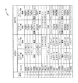
本開示の例示的な実施形態により、様々なカードフォーマットの多くが再目的化され得るが、本明細書に示されるのはほんの一部にすぎない。一般に、再目的化(repurposing)は、データ専用のピン、または予約されたピンを採用し、そのようなピンを使用して、差動M-PHYデータ信号を運ぶ差動データピンペアを形成する。クロック信号、電力信号、および挿入検出ピンが残され得る。この一般的な再目的化は、特に検討されているが、既存のフォームファクタのピンの目的を完全に入れ替える他の再目的化が考えられる。これに関連して、図2Aに関して、チャート42が提供されて、シリアル周辺機器インターフェース(SPI)モードの対応するSDカードコネクタへのM-PHY規格対応のピン名のマッピングを示す。詳細には、図2Aは、データ入力(DI)ライン、予備(RSV)ライン、データ出力(DO)ライン、および第2のRSVライン用のピンが、そのそれぞれのSPI信号使用から、対応するM-PHY信号使用に再目的化されている。したがって、本開示の例示的な実施形態では、データ入力に使用されていたDIピンは、TXDP信号に使用され、将来の規格開発に備えて予約されていた第1のRSVピンは、TXDN信号に使用され、データ出力信号に使用されていたDOピンは、RXDN信号に使用され、将来の規格開発に備えて予約されていた第2のRSVピンは、RXDP信号に使用される。
Although many of the various card formats can be repurposed according to exemplary embodiments of the present disclosure, only a portion is shown herein. In general, repurposing takes data-only pins or reserved pins and uses such pins to form differential data pin pairs that carry differential M-PHY data signals. . Clock signals, power signals, and insertion detection pins may be left. This general repurpose is specifically considered, but other repurposes are possible that completely replace the purpose of existing form factor pins. In this regard, with respect to FIG. 2A, a
図2Bに関して、チャート44が、対応するSDカードコネクタ信号(SPI動作なし)へのM-PHY規格対応のピン名のマッピングを示す。詳細には、図2Bは、DAT0ライン、DAT1ライン、DAT2ライン、およびDAT3ライン用のピンが、そのそれぞれのSD信号使用から、対応するM-PHY信号使用に再目的化されている。したがって、本開示の例示的な実施形態では、データ入力に使用されていたDAT0ピンは、TXDP信号に使用され、データ入力に使用されていたDAT1ピンは、TXDN信号に使用され、データ出力信号に使用されていたDAT2ピンは、RXDN信号に使用され、データ出力信号に使用されていたDAT3ピンは、RXDP信号に使用される。 With reference to FIG. 2B, chart 44 shows the mapping of pin names corresponding to the M-PHY standard to corresponding SD card connector signals (no SPI operation). Specifically, in FIG. 2B, the pins for the DAT0 line, DAT1 line, DAT2 line, and DAT3 line have been repurposed from using their respective SD signals to using the corresponding M-PHY signals. Thus, in the exemplary embodiment of the present disclosure, the DAT0 pin that was used for data input is used for the TXDP signal, and the DAT1 pin that was used for data input is used for the TXDN signal and the data output signal. The DAT2 pin that was used is used for the RXDN signal, and the DAT3 pin that was used for the data output signal is used for the RXDP signal.
図2Cに関して、チャート46が、対応するUHS-IIカードコネクタ信号へのM-PHY規格対応のピン名のマッピングを示す。詳細には、図2Cは、D0+ライン、D0-ライン、D1+ライン、およびD1-ライン用のピンが、そのそれぞれのUHS-II信号使用から、対応するM-PHY信号使用に再目的化されている。したがって、本開示の例示的な実施形態では、データ入力に使用されていたD0+ピンは、TXDP信号に使用され、データ入力に使用されていたD0-ピンは、TXDN信号に使用され、データ出力信号に使用されていたD1+ピンは、RXDN信号に使用され、データ出力信号に使用されていたD0-ピンは、RXDP信号に使用される。ピン1、2、3、および5によって形成される第2のレーンはオプションであり、第2の差動レーンには4つの予約されたピンを使用することに注意されたい。
With respect to FIG. 2C, chart 46 shows the mapping of M-PHY standard compliant pin names to corresponding UHS-II card connector signals. Specifically, Figure 2C shows that the pins for D0 +, D0-, D1 +, and D1- lines have been repurposed from their respective UHS-II signal usage to the corresponding M-PHY signal usage. Yes. Thus, in the exemplary embodiment of the present disclosure, the D0 + pin that was used for data input is used for the TXDP signal, and the D0- pin that was used for data input is used for the TXDN signal and the data output signal. The D1 + pin used for the RXD signal is used for the RXDN signal, and the D0- pin used for the data output signal is used for the RXDP signal. Note that the second lane formed by
図2Dに関して、チャート48は、M-PHY規格対応のピン名の、対応するMMCplusコネクタ信号へのマッピングを示す。詳細には、図2Dは、DAT0ラインからDAT7ライン用のピンが、そのそれぞれのMMC信号使用から、対応するM-PHY信号使用に再目的化されている。したがって、本開示の例示的な実施形態では、データ入力に使用されていたDAT0ピンおよびDAT1ピンは、TXDP0信号およびTXDN0信号に使用され、データ出力に使用されていたDAT2ピンおよびDAT3ピンは、RXDN0信号およびRXDP0信号に使用され、データ入力信号に使用されていたDAT4ピンおよびDAT5ピンは、TXDP1信号およびTXDN1信号に使用され、データ出力信号に使用されていたDAT6ピンおよびDAT7ピンは、RXDN1信号およびRXDP1信号に使用される。ピン10、11、12、および13によって形成される第2のレーンはオプションであり、実装はピン1、7、8、および9によって形成される1つの差動レーンだけを使用し得ることに注意されたい。
With reference to FIG. 2D, chart 48 shows the mapping of pin names corresponding to the M-PHY standard to corresponding MMCplus connector signals. Specifically, in FIG. 2D, the pins for the DAT0 line to the DAT7 line are repurposed from using their respective MMC signals to using the corresponding M-PHY signals. Thus, in the exemplary embodiment of the present disclosure, the DAT0 and DAT1 pins that were used for data input are used for the TXDP0 and TXDN0 signals, and the DAT2 and DAT3 pins that were used for data output are RXDN0. The DAT4 and DAT5 pins used for the data and RXDP0 signals and used for the data input signal are used for the TXDP1 and TXDN1 signals, and the DAT6 and DAT7 pins used for the data output signal are the RXDN1 signal and Used for RXDP1 signal. Note that the second lane formed by
図2A〜図2Dのチャートは、特定のメモリカードフォームファクタのための再割当てを知る際に役立つが、再目的化されたメモリカードフォームファクタを見ることもまた役立つ可能性がある。これに関連して、図2Eは、ピン12A'〜ピン12I'(まとめてピン12')を有する、再目的化されたSD型メモリカードフォームファクタコネクタ10'の上面図を示す。ピン12'は、ハウジング14'内に配置されている。ハウジング14'は、図1Aのハウジング14と同一のサイズにされ、ピン12'は、図1Aのピン12と同じ場所に配置されている。しかしながら、上記の説明のように、ピン12の再目的化は、メモリカードフォームファクタコネクタ10'がM-PHYプロトコルにより動作できるようにする。さらに、実際のペアは、互いから離れている(たとえば、送信はメモリカードコネクタの一方の端部にあり、受信は反対の端部にある)が、ピンレイアウトおよび再目的化は、各差動ペアの2つのピンを互いに隣接して配置するように設計される(たとえば、ピン1およびピン9がTXDNおよびTXDP差動ペアを運び、ピン7およびピン8がRXDPおよびRXDN差動ペアを運ぶ)。ピン12'の再目的化は、以下のTABLE 4(表4)にまとめられている。
While the charts of FIGS. 2A-2D are helpful in knowing the reassignment for a particular memory card form factor, it may also be helpful to look at the repurposed memory card form factor. In this regard, FIG. 2E shows a top view of a repurposed SD memory card
メモリカード規格およびプロトコルからのデータチャネルのこの再マッピングは、従来のメモリカード用の同じフォームファクタが、M-PHY対応のデバイスで使用されることを可能にする。さらに、業界の認知度および規格化されたメモリカードフォームファクタでメモリカードを作るための定着した製造プロセスを考えると、そのような規格化されたコネクタを実装するM-PHYデバイスのための容易に利用可能な製造チェーンがあるはずである。 This remapping of data channels from memory card standards and protocols allows the same form factor for conventional memory cards to be used in M-PHY capable devices. In addition, given the industry recognition and established manufacturing process for making memory cards with a standardized memory card form factor, it is easy for M-PHY devices to implement such standardized connectors There should be a production chain available.
図3Aに関して、ピン要件を有する例示的な従来のM-PHY信号パスレイアウト50が提供される。すなわち、第1の電子デバイス52が、第2の電子デバイス54に接続される。第1の電子デバイス52は、(図6に関して以下に説明する)制御システムまたはプロセッサを含むことができ、これが適切なデバイスドライバを通じて、(本明細書ではインターフェースのための手段と呼ばれることもある)通信インターフェースの信号レーン56A、56Bを制御することができる。信号レーン56Aは、第1の電子デバイス52が、RXDPピン60AおよびRXDNピン60BへのTXDPピン58AおよびTXDNピン58Bを通じて第2の電子デバイス54にデータを送信するレーンである。同様に、第2の電子デバイス54は、RXDPピン64AおよびRXDNピン64BへのTXDPピン62AおよびTXDNピン62Bを通じて第1の電子デバイス52にデータを送信する。各電子デバイス52、54は、それぞれのレーン管理モジュール70A、70Bによって制御される、その独自のそれぞれの送信機M-TX66A、68Bと、受信機M-RX68A、66Bとを有する。レーン管理モジュール70A、70Bは、要求に応じてハードウェア、またはソフトウェア、またはこの2つの混合であってもよく、リンク78A、78Bを介して制御システムと通信することができる。ピン58A、58B、64A、64Bは、単一のMポート72にあってもよく、ピン60A、60B、62A、62Bは、それらが第2の異なるデバイス上にあることから、第2のMポート74にあると定義される。
With reference to FIG. 3A, an exemplary conventional M-PHY
引き続き図3Aに関して、レーン管理モジュール70Aは、周辺機器交換フォーマット(PIF:peripheral interchange format)リンク76Aを介して送信機66Aと、およびPIFリンク76Bを介して受信機68Aと、通信することができる。同様に、レーン管理モジュール70Bは、PIFリンク76Cを介して受信機66B、およびPIFリンク76Dを介して送信機68Bと通信することができる。レーン管理モジュール70A、70B、リンク78A、78B、送信機66A、68B、受信機66B、68A、およびPIFリンク76A〜76Dは、M-PHY規格に示されており、興味のある読者は、そこでこれらの要素に関するより多くの情報を得られる。図のように、第1の電子デバイス52は、第2の電子デバイス54に直接接続されている。明示的に示していないが、当然のことながら、直接接続は、コネクタ、ケーブル、または組合せによって代替され得る。やはり、信号およびレーン管理要素は、M-PHY規格によって定義されるが、ピンおよび任意のコネクタの配置は、未定義のままである。しかしながら、図2A〜図2Eに関して記載したように、メモリカード型コネクタは、メモリカードフォームファクタに物理的変更を求めることなく、データピンをTXDP、TXDN、RXDN、RXDP信号パスにマップすることによって、再目的化され得る。これに関連して、メモリカードフォームファクタは、本明細書では接続するための手段と呼ばれることがあってもよい。
Still referring to FIG. 3A, the
ホストデバイス24に挿入された再目的化されたメモリカードフォームファクタコネクタ10'の例示的な簡略図が、図3Bに提供されている。詳細には、メモリカードフォームファクタコネクタ10'は、適切なピン58A、58B、64A、64B(図3A)を介してホストデバイス24の送信機M-TX66Aおよび受信機M-RX68Aからの出力に結合するピン12'を有する。メモリカードフォームファクタコネクタ10'のハウジング14'の内部には、受信機66Bおよび送信機68Bならびに従来のレーン管理70Bがある。
An exemplary simplified diagram of a repurposed memory card form factor connector 10 'inserted into the
図4を見ると、フローチャートが提供され、M-PHY規格を使用して動作するように構成された、電子デバイス52などの第1の電子デバイスを、嵌合接続部(mated connection)、嵌合接続部を有するケーブルなどを介して電子デバイス54などの第2の電子デバイスに接続する方法を示している。最初に方法は、電子デバイスを提供し(ブロック100)、電子デバイスに複数のデータパスを形成する。各パスは、M-PHY規格に準拠している(ブロック102)。方法は、第1の電子デバイスに複数のピンを有するメモリカード型コネクタを提供する(ブロック104)。例示的な実施形態では、メモリカード型コネクタは、次の標準フォームファクタの1つに準拠する:SD、MMC、コンパクトフラッシュ(登録商標)、メモリスティック、SPI、xD、XQD、またはUHS。
Looking at FIG. 4, a flowchart is provided and a first electronic device, such as
引き続き図4に関して、方法は、メモリカード型フォームファクタ内のピンを、データパスに電気的に結合する(ブロック106)。例示的な実施形態では、ピンは、第1の送信ピンをM-PHY TXDPデータパスに電気的に結合し、第2の送信ピンをM-PHY TXDNデータパスに電気的に結合し、第1の受信ピンをM-PHY RXDNデータパスに電気的に結合し、第2の受信ピンをM-PHY RXDPデータパスに電気的に結合することによってマップされる。メモリカードコネクタフォームファクタが正常に4つのデータパスを持っていない場合、予約された接点が、その代わりに使用され得る。同様に、データパスが送信または受信データパスとして特に指定されていない場合、そのような指定が選択され得る。 With continued reference to FIG. 4, the method electrically couples a pin in the memory card type form factor to the data path (block 106). In the exemplary embodiment, the pin electrically couples the first transmit pin to the M-PHY TXDP data path, electrically couples the second transmit pin to the M-PHY TXDN data path, and the first Are electrically coupled to the M-PHY RXDN data path and the second receive pin is electrically coupled to the M-PHY RXDP data path. If the memory card connector form factor does not successfully have four data paths, reserved contacts can be used instead. Similarly, if the data path is not specifically designated as a transmit or receive data path, such designation may be selected.
引き続き図4に関して、およびデータパスがメモリカード型フォームファクタ内のそれぞれのピンに接続されて、第1の電子デバイスは、第2の電子デバイス(たとえば、第2のデバイス54)に接続され得る(ブロック108)。接続中またはその後すぐに、コネクタに関連する制御システムは、挿入検出を行う(ブロック110)および/または第2の電子デバイス54に電力を供給する(ブロック112)ことができる。 Continuing with FIG. 4, and with the data path connected to respective pins in the memory card type form factor, the first electronic device may be connected to a second electronic device (e.g., second device 54) ( Block 108). During or shortly after connection, the control system associated with the connector may perform insertion detection (block 110) and / or provide power to the second electronic device 54 (block 112).
上記の説明は、メモリカード型フォームファクタ内のデータパスを再目的化することに焦点を当てたが、メモリカード型フォームファクタ内には、挿入検出および/または電力供給などの他の目的に使用され得る他のピンがある。たとえば、ほとんどのメモリカードは、電源ピンを含む。電源ピンの存在は、挿入検出を可能にし、第2の電子デバイス54に電力を供給する能力を与える。挿入検出により、第1の電子デバイス52は、データを送るまたは第2の電子デバイス54からのデータをリッスンすることがいつ許容できるかを知ることができる。同様に、第2の電子デバイス54は、第1の電子デバイス52が接続されたことを検出するはずである。挿入検出を通して他の利点も実現される可能性があり、本開示はこれに限るものではない。同様に、第2の電子デバイス54に電力を提供することにより、設計者は第2の電子デバイス54に電源コードまたは代替電源を提供する必要を回避することができる。
While the above discussion has focused on repurposed data paths within the memory card form factor, the memory card form factor may be used for other purposes such as insertion detection and / or power delivery. There are other pins that can be done. For example, most memory cards include power pins. The presence of the power pin enables insertion detection and provides the ability to power the second
同じ一般的なフォームファクタを有するが、潜在的に異なるピン構成および使用を有する非常に多くのメモリカードが存在することから、ホストデバイスが、どのタイプのカードが挿入されたかを確かめるための何らかの方法が必要である。どのタイプのカードが挿入されたかを判断するための例示的なプロセス120が、図5に示されている。プロセス120は、ブロック122から始まり、第1の電子デバイス52は、差し込み口26内のカードにCMD5メッセージを送る(ブロック124)。ブロック126においてカードが応答する場合、第1の電子デバイス52は、差し込み口26内のカードが、セキュアデジタル入力出力(SDIO:secure digital input output)カードであると判断する(ブロック128)。しかしながら、ブロック126において応答が得られない場合、第1の電子デバイス52は、差し込み口26内のカードにCMD41メッセージを送る(ブロック130)。ブロック132においてカードが応答する場合、第1の電子デバイス52は、差し込み口26内のカードが、SDカードであると判断する(ブロック134)。しかしながら、ブロック132において応答が得られない場合、第1の電子デバイス52は、差し込み口26内のカードにCMD1メッセージを送る(ブロック136)。
Since there are so many memory cards that have the same general form factor but potentially different pin configurations and uses, the host device has some way to see what type of card is inserted is necessary. An
引き続き図5に関して、ブロック138においてカードが応答する場合、第1の電子デバイス52は、差し込み口26内のカードが、MMCであると判断する(ブロック140)。しかしながら、ブロック138において応答が得られない場合、第1の電子デバイス52は、差し込み口26内のカードは、M-PHYプロトコルに従って動作していると推論し、M-PHYインターフェースに変え、カードにアクセスしようと試みる(ブロック142)。ブロック144において差し込み口26内のカードが応答する場合、ホストデバイス52は、差し込み口26内のカードが、M-PHY対応のデバイスであると判断する(ブロック146)。差し込み口26内のカードが依然として応答しない場合、プロセスはエラーを生成する(ブロック148)。
Continuing with FIG. 5, if the card responds at
プロセス120は、差し込み口26に挿入されたカードが特定のタイプのカードであったかどうかを判断するための特定のコマンドについて検討し、説明しているが、当然のことながら、これらのカードタイプの各々に対する規格は、複数の一意のコマンド(すなわち、その規格に対してのみ存在し、他の規格には対応するコマンドがないコマンド(たとえば、SDに対してのみ存在するが、MMC、UHSなどに対しては存在しないコマンド))を有する。したがって、本開示の範囲を逸脱することなくどのカードタイプが挿入されているかについて判断する助けとなるように他のコマンドが使用され得る。
上記の説明は、メモリカードフォームファクタ内のピンを再目的化することに焦点を当てたが、本開示はこれに限らない。さらに、本開示は、メモリカードフォームファクタと併せてユニバーサルフラッシュストレージ(UFS:Universal Flash Storage)ストレージシステムを使用することを考える。UFSは従来、コンピューティングデバイスのボードにはんだ付けされたフラッシュメモリなどの固定メモリユニットに対してのみ提案されていることに注意されたい。参照によってその全体をこれにより組み込まれている、2011年10月12日公表のYuping ChungによるJEDEC公表UFS PHY and UNIPRO(登録商標)から明らかであるように、UFSは、M-PHYプロトコルと強く結びついている。ChungはM-PHY物理層を通して実装されるUFSを検討するが、Chungは、取り外し可能なメモリカードでUFSを使用すること、または上述のように標準化されたコネクタを介してM-PHYを使用して、メモリカードと通信することを検討しない。本開示は、既存のUFS機能を、取り外し可能なメモリカードコネクタに使用可能にすること、容易に利用可能なカードフォームファクタを使用すること、および本明細書に開示する再目的化技法によって、これを拡張することを考える。 Although the above description has focused on repurpose pins within a memory card form factor, the present disclosure is not so limited. Furthermore, this disclosure contemplates using a Universal Flash Storage (UFS) storage system in conjunction with a memory card form factor. Note that UFS has traditionally been proposed only for fixed memory units such as flash memory soldered to the board of a computing device. UFS is strongly associated with the M-PHY protocol, as is evident from JEDEC's published UFS PHY and UNIPRO® by Yuping Chung, published October 12, 2011, which is hereby incorporated by reference in its entirety. ing. Chung considers UFS implemented through the M-PHY physical layer, but Chung uses UFS with removable memory cards, or uses M-PHY through standardized connectors as described above. And do not consider communicating with memory cards. This disclosure makes this possible by making existing UFS functionality available to removable memory card connectors, using readily available card form factors, and the re-purpose techniques disclosed herein. Think about extending.
本開示は、様々なメモリカード規格からM-PHY使用へ特定のピンを再目的化することに焦点を当てているが、メモリカードフォームファクタ上のいかなるピンも、送信機および受信機差動ペアを保持するように再目的化され得ることに注意されたい。設計の選択の問題として、M-PHY使用下で送信機および受信機差動ペアとして働くようにメモリカードフォームファクタからのデータピンを再目的化することの方がより理にかなっている。同様に、多くの場合、M-PHY使用において他のメモリカードフォームファクタピンの目的を保つことは理にかなっている。たとえば、グラウンド接続をグラウンド接続として保つことは理にかなっている。同様に、電源ピンとして指定されているピンは、M-PHYシステムにおいて電源ピンとして保たれ得る。ピン機能のそのような保存は、相互運用性を促進し、1つのシステムに詳しい設計者が再目的化されたシステムにおけるピンレイアウトに容易に適応することを可能にする。SDおよびMMCplusのみが明確に示されているが、それによって示される再目的化の概念は、コンパクトフラッシュ(登録商標)(IおよびII)、セキュアデジタル(SD)(SD、miniSD、microSD、SDHC、miniSDHC、microSDHC、SDXC)、メモリスティック(スタンダード、Pro、Pro Duo、Pro-HG Duo、Micro(M2)、xC)、MultiMediaCard(MMC)(MMC、RS-MMC、MMCmobile、MMCplus、MMCmicro、eMMC)、シリアル周辺機器インターフェース(SPI)、xD(スタンダード、Type M、Type H、Type M+)、XQD、およびウルトラハイスピード(UHS:Ultra High Speed)(IおよびII)などの、様々な他のメモリカードコネクタに適用可能であることは、繰り返して述べる価値がある。 Although this disclosure focuses on re-purpose specific pins from various memory card standards to M-PHY use, any pin on the memory card form factor can be used as a transmitter and receiver differential pair. Note that it can be repurposed to preserve As a matter of design choice, it makes more sense to repurpose the data pins from the memory card form factor to work as a transmitter and receiver differential pair under M-PHY. Similarly, in many cases, it makes sense to preserve the purpose of other memory card form factor pins when using M-PHY. For example, it makes sense to keep a ground connection as a ground connection. Similarly, pins that are designated as power pins can be kept as power pins in the M-PHY system. Such preservation of pin functionality facilitates interoperability and allows designers familiar with one system to easily adapt to the pin layout in a repurposed system. Only SD and MMCplus are clearly shown, but the concept of repurposes shown by them is CompactFlash (I and II), Secure Digital (SD) (SD, miniSD, microSD, SDHC, miniSDHC, microSDHC, SDXC), Memory Stick (Standard, Pro, Pro Duo, Pro-HG Duo, Micro (M2), xC), MultiMediaCard (MMC) (MMC, RS-MMC, MMCmobile, MMCplus, MMCmicro, eMMC), Various other memory card connectors such as Serial Peripheral Interface (SPI), xD (Standard, Type M, Type H, Type M +), XQD, and Ultra High Speed (UHS) (I and II) It is worth reiterating that it is applicable.
補足説明として、共有クロックの使用は、(既存のクロックピンを使用して、またはクロック信号を運ぶように再目的化された異なるピンを使用して)行われ得る。共有クロックの使用は、M-PHYタイプIIの利用を可能にし、UFSがクロック信号を必要とするので、(M-PHYタイプIはクロックを必要としないが)M-PHYタイプIを使用するUFSにも合致する。 As a side note, the use of a shared clock can be done (using existing clock pins or using different pins repurposed to carry clock signals). The use of a shared clock allows the use of M-PHY Type II and UFS uses M-PHY Type I (though M-PHY Type I does not require a clock) because UFS requires a clock signal. It also matches.
図示していないが代替的実施形態では、メモリは、TXDP/TXDNペアのみを必要とする書き込み専用メモリであってもよく、したがってデータ伝送に2つのピンしか必要とされないことになる。そのような利用の例示的な状況は、監視局、センサアレイ(sensory array)、または遠隔測定システムが、データをメモリに書き込むが、これを決して読み返さない(たとえば、監視者、ロケット、気象観測気球、航空機ブラックボックスなどに書き込まれる)ことであろう。 In an alternative embodiment, not shown, the memory may be a write-only memory that requires only a TXDP / TXDN pair, so only two pins are required for data transmission. An exemplary situation for such use is when a monitoring station, sensory array, or telemetry system writes data to memory but never reads it back (e.g., a supervisor, rocket, weather observation) Will be written in balloons, aircraft black boxes, etc.).
本明細書に開示される実施形態により、メモリカードフォームファクタインターフェースを使用するM-PHY通信プロトコルの運用、ならびに関連するデバイス、システム、および方法は、任意のプロセッサベースのデバイスにおいて提供され得る、またはこれに統合され得る。例は、セットトップボックス、エンターテイメントユニット、ナビゲーションデバイス、通信デバイス、固定位置データユニット、モバイル位置データユニット、携帯電話、セルラ電話またはスマートフォン、コンピュータ、ポータブルコンピュータ、デスクトップコンピュータ、携帯情報端末(PDA)、モニタ、コンピュータモニタ、テレビ、チューナ、ラジオ、衛星ラジオ、音楽プレーヤ、デジタル音楽プレーヤ、ポータブル音楽プレーヤ、デジタルビデオプレーヤ、ビデオプレーヤ、デジタルビデオディスク(DVD)プレーヤ、およびポータブルデジタルビデオプレーヤを含むが、これらに限らない。 According to embodiments disclosed herein, operation of an M-PHY communication protocol using a memory card form factor interface, and associated devices, systems, and methods may be provided in any processor-based device, or It can be integrated into this. Examples are set-top boxes, entertainment units, navigation devices, communication devices, fixed location data units, mobile location data units, mobile phones, cellular phones or smartphones, computers, portable computers, desktop computers, personal digital assistants (PDAs), monitors Computer monitors, televisions, tuners, radios, satellite radios, music players, digital music players, portable music players, digital video players, video players, digital video disc (DVD) players, and portable digital video players. Not exclusively.
これに関連して、図6は、図2A〜図2Dのマッピング(または、本明細書に開示する他の概念に合致する他のマッピング)を適用してメモリカード型コネクタを使用することができるプロセッサベースのシステム170の例を示す。コントローラ200が、図のようにレーン管理モジュール70Aと相互運用する。図6のために、メモリカード型コネクタは、コネクタ202と呼ぶ。この例では、プロセッサベースのシステム170は、1つまたは複数の中央処理装置(CPU)172を含み、各CPUが1つまたは複数のプロセッサ174を含んでいる。CPU172は、マスターデバイスであってもよい。CPU172は、一時的に記憶されたデータへの高速アクセスのためにプロセッサ174に結合されたキャッシュメモリ176を有することができる。CPU172は、システムバス180に結合され、プロセッサベースのシステム170に含まれるマスターデバイスおよびスレーブデバイスを相互結合することができる。システムバス180は、バス相互接続であってよい。よく知られているように、CPU172は、システムバス180を通じてアドレス、制御、およびデータ情報を交換することによって、これらの他のデバイスと通信する。たとえば、CPU172は、スレーブデバイスの一例として、メモリコントローラ168(N)にバストランザクション要求を通信することができる。図6には示していないが、複数のシステムバス180が設けられることが可能であり、各システムバス180が異なる構造(fabric)を構成する。
In this regard, FIG. 6 can use the memory card type connector applying the mapping of FIGS. 2A-2D (or other mappings consistent with other concepts disclosed herein). An example of a processor-based
他のマスターデバイスおよびスレーブデバイスが、システムバス180に接続され得る。図6に示すように、これらのデバイスは、例として、メモリシステム182、1つまたは複数の入力デバイス184、1つまたは複数の出力デバイス186、1つまたは複数のネットワークインターフェースデバイス188、および1つまたは複数のディスプレイコントローラ190を含むことができる。入力デバイス184は、入力キー、スイッチ、音声プロセッサなどを含む、ただしこれらに限らない、いかなるタイプの入力デバイスも含むことができる。出力デバイス186は、オーディオ、ビデオ、他の視覚的表示器などを含む、ただしこれらに限らない、いかなるタイプの出力デバイスも含むことができる。ネットワークインターフェースデバイス188は、ネットワーク192へのおよびネットワーク192からのデータの交換を可能にするように構成されたいかなるデバイスでもあり得る。ネットワーク192は、有線またはワイヤレスネットワーク、プライベートまたはパブリックネットワーク、ローカルエリアネットワーク(LAN)、ワイドローカルエリアネットワーク(WLAN)、およびインターネットを含む、ただしこれらに限らない、いかなるタイプのネットワークでもあり得る。ネットワークインターフェースデバイス188は、所望のいかなるタイプの通信プロトコルもサポートするように構成され得る。メモリシステム182は、1つまたは複数のメモリユニット193(0〜N)を含むことができる。アービタは、システムバス180と、たとえばメモリシステム182に設けられたメモリユニット193(0〜N)など、システムバス180に結合されたマスターデバイスおよびスレーブデバイスとの間に設けられ得る。
Other master devices and slave devices may be connected to the
CPU172はまた、システムバス180を介してディスプレイコントローラ190にアクセスして、1つまたは複数のディスプレイ194に送られる情報を制御するように構成することもできる。ディスプレイコントローラ190は、1つまたは複数のビデオプロセッサ196を介して表示されるようにディスプレイ194に情報を送り、1つまたは複数のビデオプロセッサ196は、表示される情報を処理して、ディスプレイ194に適したフォーマットにする。ディスプレイ194は、陰極線管(CRT)、液晶ディスプレイ(LCD)、プラズマディスプレイなどを含む、ただしこれに限らない、いかなるタイプのディスプレイも含むことができる。
CPU172およびディスプレイコントローラ190は、システムバス180を通じてアービタへのメモリアクセス要求を行うためのマスターデバイスとして働くことができる。CPU172およびディスプレイコントローラ190内の様々なスレッドが、アービタへの要求を行うことができる。
The
本明細書に開示する実施形態に関連して説明する様々な例示的論理ブロック、モジュール、回路、およびアルゴリズムは、電子ハードウェア、メモリにもしくは別のコンピュータ可読媒体に記憶され、プロセッサもしくは他の処理デバイスによって実行される命令、または両方の組合せとして実装され得ることは、当業者にはさらに理解されよう。本明細書に記載するアービタ、マスターデバイス、およびスレーブデバイスは、例として、いかなる回路、ハードウェアコンポーネント、集積回路(IC)、またはICチップにおいても、使用され得る。本明細書に開示するメモリは、いかなるタイプおよびサイズのメモリであってもよく、所望のいかなるタイプの情報も記憶するように構成され得る。このような互換性をわかりやすく説明するために、様々な例示的な構成要素、ブロック、モジュール、回路、およびステップを、概してその機能に関して上述した。そのような機能がいかにして実装されるかは、システム全体に課される特定の用途、設計選択、および/または設計制約によって決まる。当業者は、特定の用途ごとに様々な方法で、記載した機能を実装することができるが、そのような実装の決定は、本開示の範囲からの逸脱を生じさせると解釈されるべきではない。 Various exemplary logic blocks, modules, circuits, and algorithms described in connection with the embodiments disclosed herein are stored in electronic hardware, memory, or in another computer-readable medium, and are processor or other processing. One skilled in the art will further appreciate that it may be implemented as instructions executed by the device, or a combination of both. The arbiters, master devices, and slave devices described herein may be used in any circuit, hardware component, integrated circuit (IC), or IC chip, by way of example. The memory disclosed herein may be any type and size of memory and may be configured to store any type of information desired. To clearly illustrate such compatibility, various illustrative components, blocks, modules, circuits, and steps have been described above generally in terms of their functionality. How such functionality is implemented depends on the specific application, design choices, and / or design constraints imposed on the overall system. Those skilled in the art can implement the described functionality in a variety of ways for a particular application, but such implementation decisions should not be construed as causing a departure from the scope of this disclosure. .
本明細書に開示する実施形態と関連して説明する様々な例示的論理ブロック、モジュール、および回路は、プロセッサ、デジタル信号プロセッサ(DSP)、特定用途用集積回路(ASIC)、フィールドプログラマブルゲートアレイ(FPGA)もしくは他のプログラマブルロジックデバイス、個別のゲートもしくはトランジスタロジック、個別のハードウェアコンポーネント、または本明細書に記載した機能を行うように設計されたこれらの任意の組合せを用いて、実装または実行され得る。プロセッサは、マイクロプロセッサとすることができるが、代替的にプロセッサは、いかなる従来のプロセッサ、コントローラ、マイクロコントローラ、または状態機械とすることもできる。プロセッサは、たとえばDSPとマイクロプロセッサの組合せ、複数のマイクロプロセッサ、DSPコアと連結した1つもしくは複数のマイクロプロセッサ、または任意の他のそのような構成など、コンピューティングデバイスの組合せとしても実装され得る。 Various exemplary logic blocks, modules, and circuits described in connection with the embodiments disclosed herein include processors, digital signal processors (DSPs), application specific integrated circuits (ASICs), field programmable gate arrays ( FPGA) or other programmable logic device, individual gate or transistor logic, individual hardware components, or any combination of these designed to perform the functions described herein. obtain. The processor can be a microprocessor, but alternatively the processor can be any conventional processor, controller, microcontroller, or state machine. A processor may also be implemented as a combination of computing devices, such as a combination of DSP and microprocessor, multiple microprocessors, one or more microprocessors coupled to a DSP core, or any other such configuration. .
本明細書に開示する実施形態は、ハードウェアにおいて、およびハードウェアに記憶されている命令において具体化されることが可能であり、たとえば、ランダムアクセスメモリ(RAM)、フラッシュメモリ、リードオンリメモリ(ROM)、電気的プログラム可能ROM(EPROM:Electrically Programmable ROM)、電気的消去可能プログラム可能ROM(EEPROM:Electrically Erasable Programmable ROM)、レジスタ、ハードディスク、リムーバブルディスク、CD-ROM、または当技術分野で知られているその他の形式のコンピュータ可読媒体に、常駐することが可能である。プロセッサが記憶媒体から情報を読み取ること、および記憶媒体に情報を書き込むことができるように、例示的記憶媒体がプロセッサに結合される。代替的に記憶媒体は、プロセッサと一体化され得る。プロセッサおよび記憶媒体は、ASIC内に存在し得る。ASICは、遠隔局に存在し得る。代替的にプロセッサおよび記憶媒体は、遠隔局、基地局、またはサーバに個別構成要素として存在し得る。 Embodiments disclosed herein may be embodied in hardware and in instructions stored in hardware, for example, random access memory (RAM), flash memory, read only memory ( ROM, Electrically Programmable ROM (EPROM), Electrically Erasable Programmable ROM (EEPROM), Register, Hard Disk, Removable Disk, CD-ROM, or known in the art It can reside on other forms of computer readable media. An exemplary storage medium is coupled to the processor such that the processor can read information from, and write information to, the storage medium. In the alternative, the storage medium may be integral to the processor. The processor and the storage medium may reside in an ASIC. The ASIC can reside at a remote station. In the alternative, the processor and the storage medium may reside as discrete components in a remote station, base station, or server.
本明細書の例示的な実施形態のいずれかに記載する動作ステップは、例および説明を提供するために記載されていることにも注意されたい。記載する動作は、例示の順序以外の数多くの異なる順序で行われ得る。さらに、単一の動作ステップに記載する動作が、実際にはいくつかの異なるステップで行われ得る。その上、例示的な実施形態に記載される1つまたは複数の動作ステップは、結合され得る。フローチャート図に示す動作ステップは、当業者には容易にわかるように、数多くの異なる変更の影響を受ける可能性がある。情報および信号は、多種多様な技術および技法のいずれかを使用して表され得ることもまた、当業者には理解されよう。たとえば、上記の説明全体を通して参照され得るデータ、命令、コマンド、情報、信号、ビット、シンボル、およびチップは、電圧、電流、電磁波、磁場もしくは磁性粒子、光場もしくは光粒子、またはその任意の組合せによって表され得る。 Note also that the operational steps described in any of the exemplary embodiments herein are set forth to provide examples and explanations. The operations described can be performed in a number of different orders other than the illustrated order. Furthermore, the operations described in a single operation step can actually be performed in several different steps. Moreover, one or more operational steps described in the exemplary embodiments can be combined. The operational steps shown in the flowchart diagrams can be affected by many different changes, as will be readily appreciated by those skilled in the art. Those skilled in the art will also appreciate that information and signals may be represented using any of a variety of different technologies and techniques. For example, data, instructions, commands, information, signals, bits, symbols, and chips that may be referred to throughout the above description are voltages, currents, electromagnetic waves, magnetic fields or magnetic particles, light fields or light particles, or any combination thereof Can be represented by:
本開示についての前述の説明は、当業者が本開示を作成または利用することができるように提供する。本開示への様々な変更形態が当業者には容易に理解されることになり、本明細書で規定する包括的な原理は、本開示の趣旨または範囲から逸脱することなく他の変形形態に適用され得る。したがって、本開示は、本明細書に記載する例および設計に限定されるものではなく、本明細書で開示する原理および新規の特徴に合致する最も広い範囲を与えられるべきである。 The previous description of the disclosure is provided to enable any person skilled in the art to make or use the disclosure. Various modifications to the present disclosure will be readily apparent to those skilled in the art, and the generic principles defined herein may be modified in other ways without departing from the spirit or scope of the present disclosure. Can be applied. Accordingly, the present disclosure is not intended to be limited to the examples and designs described herein, but is to be accorded the widest scope consistent with the principles and novel features disclosed herein.
10 SDカード
12 ピン
14 ハウジング
16 マルチメディアカード
18 ピン
20 ハウジング
22 従来のカード
24 ホスト
26 差し込み口
28 送信要素
30 受信要素
32 電気接点
34 ピン
36 受信要素
38 送信要素
40 コンピュータ可読メモリ
50 M-PHY信号パスレイアウト
52 電子デバイス
54 電子デバイス
56 信号レーン
58 ピン
60 ピン
62 ピン
64 ピン
66 送信機、受信機
68 送信機、受信機
70 レーン管理モジュール
72 Mポート
74 Mポート
76 周辺機器交換フォーマット(PIF)リンク
78 リンク
172 中央処理装置(CPU)
174 プロセッサ
176 キャッシュメモリ
180 システムバス
182 メモリシステム
184 入力デバイス
186 出力デバイス
188 ネットワークインターフェースデバイス
190 ディスプレイコントローラ
192 ネットワーク
193 メモリユニット
194 ディスプレイ
196 ビデオプロセッサ
200 コントローラ
202 コネクタ
10 SD card
12 pin
14 Housing
16 Multimedia card
18 pin
20 Housing
22 Conventional card
24 hosts
26 slot
28 Sending elements
30 receiving elements
32 Electrical contacts
34 pin
36 Receiving element
38 Sending elements
40 computer readable memory
50 M-PHY signal path layout
52 Electronic devices
54 Electronic devices
56 signal lanes
58 pins
60 pins
62 pin
64-pin
66 Transmitter, receiver
68 Transmitter, receiver
70 lane management module
72 M port
74 M port
76 Peripheral Device Exchange Format (PIF) link
78 links
172 Central processing unit (CPU)
174 processor
176 cache memory
180 System bus
182 Memory system
184 Input device
186 Output device
188 Network interface device
190 Display controller
192 network
193 Memory unit
194 displays
196 video processor
200 controller
202 connector
Claims (20)
メモリカードフォームファクタ差し込み口へのメモリカードコネクタの挿入を検出するステップと、
前記メモリカードコネクタがメモリカードと関連付けられているかどうか、または前記メモリカードコネクタがM-PHYプロトコルに従って動作するように構成された回路と関連付けられているかどうかを判断するステップと、
前記判断するステップが、前記メモリカードコネクタが前記メモリカードと関連付けられていると判断する場合、第1のモードで動作するステップと、
前記判断するステップが、前記メモリカードコネクタが前記M-PHYプロトコルに従って動作するように構成された前記回路と関連付けられていると判断する場合、第2のモードで動作するステップと
を含む、方法。 A method of checking which type of card is inserted into the host device slot,
Detecting the insertion of a memory card connector into the memory card form factor slot;
Determining whether the memory card connector is associated with a memory card or whether the memory card connector is associated with a circuit configured to operate according to an M-PHY protocol;
If the determining step determines that the memory card connector is associated with the memory card, the step of operating in a first mode;
Operating in a second mode if the determining step determines that the memory card connector is associated with the circuit configured to operate according to the M-PHY protocol.
メモリカードフォームファクタ差し込み口へのメモリカードコネクタの挿入を検出するステップと、
前記メモリカードコネクタ内の論理手段に、第1のメモリカード通信プロトコルと一意に関連付けられる第1のコマンドを提供するステップと、
前記第1のコマンドへの第1の応答が、前記メモリカードコネクタ内の前記論理手段からホストデバイスに提供されるかどうかを判断するステップと、
第1の応答が提供されない場合、前記メモリカードコネクタ内の前記論理手段に、第2のメモリカード通信プロトコルと関連付けられる第2のコマンドを提供するステップと、
前記第2のコマンドへの第2の応答が、前記メモリカードコネクタ内の前記論理手段から前記ホストデバイスに提供されるかどうかを判断するステップと、
第2の応答が提供されない場合、M-PHYプロトコルに従って前記メモリカードコネクタを通じて前記メモリカードコネクタと関連付けられた回路と対話するステップと
を含む、方法。 A method of checking which type of card is inserted into the host device slot,
Detecting the insertion of a memory card connector into the memory card form factor slot;
Providing logic means within the memory card connector with a first command uniquely associated with a first memory card communication protocol;
Determining whether a first response to the first command is provided to the host device from the logic means in the memory card connector;
Providing a second command associated with a second memory card communication protocol to the logic means in the memory card connector if a first response is not provided;
Determining whether a second response to the second command is provided to the host device from the logic means in the memory card connector;
Interacting with circuitry associated with the memory card connector through the memory card connector according to an M-PHY protocol if a second response is not provided.
前記メモリカードコネクタがメモリカードと関連付けられているかどうか、または前記メモリカードコネクタがM-PHYプロトコルに従って動作するように構成された回路と関連付けられているかどうかを判断し、
前記判断が、前記メモリカードコネクタが前記メモリカードと関連付けられていると判断する場合、第1のモードで動作し、
前記判断が、前記メモリカードコネクタが前記M-PHYプロトコルに従って動作するように構成された前記回路と関連付けられていると判断する場合、第2のモードで動作する
ための命令を有するソフトウェアを含む非一時的コンピュータ可読記録媒体。 Detects insertion of a memory card connector into the memory card form factor slot,
Determining whether the memory card connector is associated with a memory card or whether the memory card connector is associated with a circuit configured to operate according to an M-PHY protocol;
If the determination determines that the memory card connector is associated with the memory card, operates in a first mode;
If the determination determines that the memory card connector is associated with the circuit configured to operate according to the M-PHY protocol, the software includes a software having instructions to operate in a second mode. Temporary computer-readable recording medium.
前記電気接点に動作可能に結合され、
前記差し込み口への前記メモリカードコネクタの挿入を検出し、
前記メモリカードコネクタがメモリカードと関連付けられているかどうか、または前記メモリカードコネクタがM-PHYプロトコルに従って動作するように構成された回路と関連付けられているかどうかを判断し、
前記判断が、前記メモリカードコネクタが前記メモリカードと関連付けられていると判断する場合、第1のモードで動作し、
前記判断が、前記メモリカードコネクタが前記M-PHYプロトコルに従って動作するように構成された前記回路と関連付けられていると判断する場合、第2のモードで動作する
ように構成された制御システムと
を含む、コンピューティングデバイス。 An outlet having an electrical contact configured to receive a memory card connector and configured to mate with a contact in a memory card form factor;
Operably coupled to the electrical contact;
Detecting the insertion of the memory card connector into the slot;
Determining whether the memory card connector is associated with a memory card or whether the memory card connector is associated with a circuit configured to operate according to an M-PHY protocol;
If the determination determines that the memory card connector is associated with the memory card, operates in a first mode;
A control system configured to operate in a second mode if the determination determines that the memory card connector is associated with the circuit configured to operate according to the M-PHY protocol; Including computing devices.
Applications Claiming Priority (7)
| Application Number | Priority Date | Filing Date | Title |
|---|---|---|---|
| US201361867343P | 2013-08-19 | 2013-08-19 | |
| US201361867353P | 2013-08-19 | 2013-08-19 | |
| US61/867,353 | 2013-08-19 | ||
| US61/867,343 | 2013-08-19 | ||
| US14/267,983 | 2014-05-02 | ||
| US14/267,983 US9137335B2 (en) | 2013-08-19 | 2014-05-02 | Operating M-PHY based communications over mass storage-based interfaces, and related connectors, systems and methods |
| PCT/US2014/051482 WO2015026717A1 (en) | 2013-08-19 | 2014-08-18 | Operating m-phy based communications over mass storage-based interfaces, and related connectors, systems and methods |
Publications (2)
| Publication Number | Publication Date |
|---|---|
| JP2016534420A JP2016534420A (en) | 2016-11-04 |
| JP6069586B2 true JP6069586B2 (en) | 2017-02-01 |
Family
ID=52466809
Family Applications (2)
| Application Number | Title | Priority Date | Filing Date |
|---|---|---|---|
| JP2016515956A Active JP6069586B2 (en) | 2013-08-19 | 2014-08-18 | Operating M-PHY based communications through mass storage based interfaces and associated connectors, systems, and methods |
| JP2016536351A Expired - Fee Related JP6549579B2 (en) | 2013-08-19 | 2014-08-18 | Operating M-PHY based communication through mass storage based interface and associated connectors, systems and methods |
Family Applications After (1)
| Application Number | Title | Priority Date | Filing Date |
|---|---|---|---|
| JP2016536351A Expired - Fee Related JP6549579B2 (en) | 2013-08-19 | 2014-08-18 | Operating M-PHY based communication through mass storage based interface and associated connectors, systems and methods |
Country Status (7)
| Country | Link |
|---|---|
| US (2) | US9674310B2 (en) |
| EP (2) | EP3036691A1 (en) |
| JP (2) | JP6069586B2 (en) |
| KR (2) | KR20160042921A (en) |
| CN (2) | CN105474238B (en) |
| CA (2) | CA2917817A1 (en) |
| WO (2) | WO2015026716A1 (en) |
Families Citing this family (11)
| Publication number | Priority date | Publication date | Assignee | Title |
|---|---|---|---|---|
| US9552318B2 (en) * | 2014-06-04 | 2017-01-24 | Qualcomm Incorporated | Removable memory card type detection systems and methods |
| US11037042B2 (en) | 2016-12-29 | 2021-06-15 | Samsung Electronics Co., Ltd. | Semiconductor integrated circuit cards and communication systems including the same |
| KR20180077727A (en) | 2016-12-29 | 2018-07-09 | 삼성전자주식회사 | Semiconductor integrated circuit card and communication system having the same |
| KR20190051530A (en) | 2017-11-07 | 2019-05-15 | 에스케이하이닉스 주식회사 | Data processing system and operating method of data processing system |
| US10353840B2 (en) | 2017-11-27 | 2019-07-16 | Motorola Solutions, Inc. | Secure digital format card having two interfaces to communicate with two processors |
| US10940959B2 (en) | 2018-10-05 | 2021-03-09 | Simmonds Precision Products, Inc. | Configurable distributed health monitoring system for a landing system |
| CN111783484A (en) * | 2019-04-04 | 2020-10-16 | 深圳市江波龙电子股份有限公司 | Identification method of memory card, electronic equipment and computer storage medium |
| JP2021162907A (en) * | 2020-03-30 | 2021-10-11 | キヤノン株式会社 | Communication device, control method, and program |
| TW202236821A (en) | 2021-03-08 | 2022-09-16 | 韓商愛思開海力士有限公司 | Method for information configuration in power mode change for an interconnection protocol, controller and storage device |
| US11902366B2 (en) | 2022-05-25 | 2024-02-13 | Bank Of America Corporation | System for implementing dynamic multi-factor soft lock on user identifiers |
| US20240126431A1 (en) * | 2022-10-14 | 2024-04-18 | Qualcomm Incorporated | Configurable flash memory physical interface in a host device |
Family Cites Families (28)
| Publication number | Priority date | Publication date | Assignee | Title |
|---|---|---|---|---|
| US5555510A (en) * | 1994-08-02 | 1996-09-10 | Intel Corporation | Automatic computer card insertion and removal algorithm |
| US5589719A (en) * | 1995-03-10 | 1996-12-31 | Fiset; Peter D. | Card out of socket detector for IC cards |
| US5568610A (en) * | 1995-05-15 | 1996-10-22 | Dell Usa, L.P. | Method and apparatus for detecting the insertion or removal of expansion cards using capacitive sensing |
| US5805903A (en) * | 1996-05-21 | 1998-09-08 | Compaq Computer Corporation | Protection of computer system against incorrect card insertion during start-up |
| US6062480A (en) * | 1998-07-20 | 2000-05-16 | Vlsi Technologies, Inc. | Hot docking system and methods for detecting and managing hot docking of bus cards |
| FI107973B (en) | 1999-03-11 | 2001-10-31 | Nokia Mobile Phones Ltd | Method and means for using option cards in a mobile station |
| JP3655597B2 (en) | 2002-03-25 | 2005-06-02 | 株式会社東芝 | Electronic device, electronic card, and card identification method |
| TWI222028B (en) | 2002-06-07 | 2004-10-11 | Carry Computer Eng Co Ltd | Switching method and judgment method of common connector and terminals of memory card |
| KR100440972B1 (en) | 2002-07-27 | 2004-07-21 | 삼성전자주식회사 | Apparatus and method for establishing data transfer mode by card insertion identification |
| US7664902B1 (en) | 2004-03-16 | 2010-02-16 | Super Talent Electronics, Inc. | Extended SD and microSD hosts and devices with USB-like high performance packetized interface and protocol |
| JP4676163B2 (en) | 2004-04-30 | 2011-04-27 | 株式会社リコー | CARD ACCESS DEVICE AND ELECTRONIC DEVICE WITH THE SAME |
| US7464213B2 (en) | 2004-12-24 | 2008-12-09 | Sony Corporation | Memory adapter and unit including independent radio circuit and removable memory store |
| JP4817836B2 (en) * | 2004-12-27 | 2011-11-16 | 株式会社東芝 | Card and host equipment |
| KR100589227B1 (en) * | 2005-05-23 | 2006-06-19 | 엠텍비젼 주식회사 | Apparatus capable of multi-interfacing memories and interfacing method of the same |
| TWM328041U (en) | 2007-05-16 | 2008-03-01 | Genesys Logic Inc | Card reader controlling apparatus based on secure digital protocol |
| US8359418B2 (en) | 2009-02-26 | 2013-01-22 | Sandisk Il Ltd. | Host device with USB interface |
| US8301822B2 (en) | 2009-09-23 | 2012-10-30 | Sandisk Il Ltd. | Multi-protocol storage device bridge |
| KR101679430B1 (en) * | 2010-09-30 | 2016-11-25 | 삼성전자주식회사 | Method and apparatus for detecting of sim card inserting in a portable terminal |
| US20120185663A1 (en) | 2011-01-14 | 2012-07-19 | Satoshi Yokoya | Memory Interface Converter |
| KR20120119092A (en) * | 2011-04-20 | 2012-10-30 | 삼성전자주식회사 | Semiconductor memory system and operating method thereof |
| JP5677336B2 (en) * | 2011-08-01 | 2015-02-25 | 株式会社東芝 | Memory device |
| US20130272368A1 (en) * | 2011-09-28 | 2013-10-17 | Wei-Lien Yang | Low power data recovery using over-clocking |
| KR101911059B1 (en) | 2011-10-18 | 2018-10-24 | 삼성전자주식회사 | Test method for UFS interface and memory device testing by the same method |
| US20130191568A1 (en) * | 2012-01-23 | 2013-07-25 | Qualcomm Incorporated | Operating m-phy based communications over universal serial bus (usb) interface, and related cables, connectors, systems and methods |
| US9081907B2 (en) * | 2012-10-29 | 2015-07-14 | Qualcomm Incorporated | Operating M-PHY based communications over peripheral component interconnect (PCI)-based interfaces, and related cables, connectors, systems and methods |
| US20140244904A1 (en) * | 2013-02-28 | 2014-08-28 | Kabushiki Kaisha Toshiba | Memory device and computer system |
| US9086966B2 (en) * | 2013-03-15 | 2015-07-21 | Intel Corporation | Systems, apparatuses, and methods for handling timeouts |
| US9563260B2 (en) * | 2013-03-15 | 2017-02-07 | Intel Corporation | Systems, apparatuses, and methods for synchronizing port entry into a low power state |
-
2014
- 2014-05-02 US US14/267,974 patent/US9674310B2/en active Active
- 2014-05-02 US US14/267,983 patent/US9137335B2/en active Active
- 2014-08-18 CN CN201480045694.9A patent/CN105474238B/en not_active Expired - Fee Related
- 2014-08-18 CA CA2917817A patent/CA2917817A1/en not_active Abandoned
- 2014-08-18 EP EP14759391.7A patent/EP3036691A1/en not_active Ceased
- 2014-08-18 CA CA2918425A patent/CA2918425A1/en not_active Abandoned
- 2014-08-18 CN CN201480045690.0A patent/CN105453108A/en active Pending
- 2014-08-18 KR KR1020167005332A patent/KR20160042921A/en active IP Right Grant
- 2014-08-18 JP JP2016515956A patent/JP6069586B2/en active Active
- 2014-08-18 KR KR1020167005334A patent/KR101678348B1/en active IP Right Grant
- 2014-08-18 WO PCT/US2014/051478 patent/WO2015026716A1/en active Application Filing
- 2014-08-18 WO PCT/US2014/051482 patent/WO2015026717A1/en active Application Filing
- 2014-08-18 JP JP2016536351A patent/JP6549579B2/en not_active Expired - Fee Related
- 2014-08-18 EP EP14759392.5A patent/EP3036682A1/en not_active Ceased
Also Published As
| Publication number | Publication date |
|---|---|
| US20150052266A1 (en) | 2015-02-19 |
| CN105474238A (en) | 2016-04-06 |
| EP3036682A1 (en) | 2016-06-29 |
| KR20160029148A (en) | 2016-03-14 |
| WO2015026716A1 (en) | 2015-02-26 |
| CA2917817A1 (en) | 2015-02-26 |
| JP2016532206A (en) | 2016-10-13 |
| CN105474238B (en) | 2018-09-21 |
| CA2918425A1 (en) | 2015-02-26 |
| US9674310B2 (en) | 2017-06-06 |
| CN105453108A (en) | 2016-03-30 |
| JP6549579B2 (en) | 2019-07-24 |
| WO2015026717A1 (en) | 2015-02-26 |
| KR20160042921A (en) | 2016-04-20 |
| US9137335B2 (en) | 2015-09-15 |
| KR101678348B1 (en) | 2016-11-21 |
| JP2016534420A (en) | 2016-11-04 |
| EP3036691A1 (en) | 2016-06-29 |
| US20150049746A1 (en) | 2015-02-19 |
Similar Documents
| Publication | Publication Date | Title |
|---|---|---|
| JP6069586B2 (en) | Operating M-PHY based communications through mass storage based interfaces and associated connectors, systems, and methods | |
| KR101561516B1 (en) | Operating m-phy based communications over pci-based interfaces, and related cables, connectors, systems and methods | |
| US20130191568A1 (en) | Operating m-phy based communications over universal serial bus (usb) interface, and related cables, connectors, systems and methods | |
| JP2011166720A (en) | Motherboard compatible with multiple versions of usb, and related method | |
| WO2017095593A1 (en) | Increased data flow in universal serial bus (usb) cables | |
| JP2019197598A (en) | Systems and methods for low voltage secure digital (sd) interfaces | |
| CN106575140B (en) | Apparatus, method and system for enabling higher current charging of a Universal Serial Bus (USB) specification version 2.0(USB 2.0) portable electronic device from a USB3.X host | |
| US9081908B2 (en) | Operating M-PHY based communications over serial advanced technology attachment (SATA)-based interface, and related cables, connectors, systems and methods |
Legal Events
| Date | Code | Title | Description |
|---|---|---|---|
| A521 | Request for written amendment filed |
Free format text: JAPANESE INTERMEDIATE CODE: A523 Effective date: 20161017 |
|
| TRDD | Decision of grant or rejection written | ||
| A01 | Written decision to grant a patent or to grant a registration (utility model) |
Free format text: JAPANESE INTERMEDIATE CODE: A01 Effective date: 20161205 |
|
| A61 | First payment of annual fees (during grant procedure) |
Free format text: JAPANESE INTERMEDIATE CODE: A61 Effective date: 20161226 |
|
| R150 | Certificate of patent or registration of utility model |
Ref document number: 6069586 Country of ref document: JP Free format text: JAPANESE INTERMEDIATE CODE: R150 |
|
| R250 | Receipt of annual fees |
Free format text: JAPANESE INTERMEDIATE CODE: R250 |
|
| R250 | Receipt of annual fees |
Free format text: JAPANESE INTERMEDIATE CODE: R250 |
|
| R250 | Receipt of annual fees |
Free format text: JAPANESE INTERMEDIATE CODE: R250 |
|
| R250 | Receipt of annual fees |
Free format text: JAPANESE INTERMEDIATE CODE: R250 |
|
| R250 | Receipt of annual fees |
Free format text: JAPANESE INTERMEDIATE CODE: R250 |