JP6050073B2 - Power storage device - Google Patents
Power storage device Download PDFInfo
- Publication number
- JP6050073B2 JP6050073B2 JP2012209931A JP2012209931A JP6050073B2 JP 6050073 B2 JP6050073 B2 JP 6050073B2 JP 2012209931 A JP2012209931 A JP 2012209931A JP 2012209931 A JP2012209931 A JP 2012209931A JP 6050073 B2 JP6050073 B2 JP 6050073B2
- Authority
- JP
- Japan
- Prior art keywords
- active material
- graphene
- shape
- storage device
- negative electrode
- Prior art date
- Legal status (The legal status is an assumption and is not a legal conclusion. Google has not performed a legal analysis and makes no representation as to the accuracy of the status listed.)
- Active
Links
Images


Classifications
-
- H—ELECTRICITY
- H01—ELECTRIC ELEMENTS
- H01M—PROCESSES OR MEANS, e.g. BATTERIES, FOR THE DIRECT CONVERSION OF CHEMICAL ENERGY INTO ELECTRICAL ENERGY
- H01M4/00—Electrodes
- H01M4/02—Electrodes composed of, or comprising, active material
-
- H—ELECTRICITY
- H01—ELECTRIC ELEMENTS
- H01M—PROCESSES OR MEANS, e.g. BATTERIES, FOR THE DIRECT CONVERSION OF CHEMICAL ENERGY INTO ELECTRICAL ENERGY
- H01M4/00—Electrodes
- H01M4/02—Electrodes composed of, or comprising, active material
- H01M4/13—Electrodes for accumulators with non-aqueous electrolyte, e.g. for lithium-accumulators; Processes of manufacture thereof
- H01M4/134—Electrodes based on metals, Si or alloys
-
- H—ELECTRICITY
- H01—ELECTRIC ELEMENTS
- H01G—CAPACITORS; CAPACITORS, RECTIFIERS, DETECTORS, SWITCHING DEVICES OR LIGHT-SENSITIVE DEVICES, OF THE ELECTROLYTIC TYPE
- H01G9/00—Electrolytic capacitors, rectifiers, detectors, switching devices, light-sensitive or temperature-sensitive devices; Processes of their manufacture
- H01G9/004—Details
- H01G9/04—Electrodes or formation of dielectric layers thereon
-
- H—ELECTRICITY
- H01—ELECTRIC ELEMENTS
- H01M—PROCESSES OR MEANS, e.g. BATTERIES, FOR THE DIRECT CONVERSION OF CHEMICAL ENERGY INTO ELECTRICAL ENERGY
- H01M12/00—Hybrid cells; Manufacture thereof
- H01M12/08—Hybrid cells; Manufacture thereof composed of a half-cell of a fuel-cell type and a half-cell of the secondary-cell type
-
- H—ELECTRICITY
- H01—ELECTRIC ELEMENTS
- H01M—PROCESSES OR MEANS, e.g. BATTERIES, FOR THE DIRECT CONVERSION OF CHEMICAL ENERGY INTO ELECTRICAL ENERGY
- H01M4/00—Electrodes
- H01M4/02—Electrodes composed of, or comprising, active material
- H01M4/13—Electrodes for accumulators with non-aqueous electrolyte, e.g. for lithium-accumulators; Processes of manufacture thereof
-
- H—ELECTRICITY
- H01—ELECTRIC ELEMENTS
- H01M—PROCESSES OR MEANS, e.g. BATTERIES, FOR THE DIRECT CONVERSION OF CHEMICAL ENERGY INTO ELECTRICAL ENERGY
- H01M4/00—Electrodes
- H01M4/02—Electrodes composed of, or comprising, active material
- H01M4/36—Selection of substances as active materials, active masses, active liquids
- H01M4/362—Composites
- H01M4/366—Composites as layered products
-
- H—ELECTRICITY
- H01—ELECTRIC ELEMENTS
- H01M—PROCESSES OR MEANS, e.g. BATTERIES, FOR THE DIRECT CONVERSION OF CHEMICAL ENERGY INTO ELECTRICAL ENERGY
- H01M4/00—Electrodes
- H01M4/02—Electrodes composed of, or comprising, active material
- H01M4/36—Selection of substances as active materials, active masses, active liquids
- H01M4/58—Selection of substances as active materials, active masses, active liquids of inorganic compounds other than oxides or hydroxides, e.g. sulfides, selenides, tellurides, halogenides or LiCoFy; of polyanionic structures, e.g. phosphates, silicates or borates
- H01M4/583—Carbonaceous material, e.g. graphite-intercalation compounds or CFx
- H01M4/587—Carbonaceous material, e.g. graphite-intercalation compounds or CFx for inserting or intercalating light metals
-
- H—ELECTRICITY
- H01—ELECTRIC ELEMENTS
- H01M—PROCESSES OR MEANS, e.g. BATTERIES, FOR THE DIRECT CONVERSION OF CHEMICAL ENERGY INTO ELECTRICAL ENERGY
- H01M4/00—Electrodes
- H01M4/02—Electrodes composed of, or comprising, active material
- H01M4/62—Selection of inactive substances as ingredients for active masses, e.g. binders, fillers
- H01M4/624—Electric conductive fillers
- H01M4/625—Carbon or graphite
-
- H—ELECTRICITY
- H01—ELECTRIC ELEMENTS
- H01M—PROCESSES OR MEANS, e.g. BATTERIES, FOR THE DIRECT CONVERSION OF CHEMICAL ENERGY INTO ELECTRICAL ENERGY
- H01M10/00—Secondary cells; Manufacture thereof
- H01M10/05—Accumulators with non-aqueous electrolyte
- H01M10/052—Li-accumulators
- H01M10/0525—Rocking-chair batteries, i.e. batteries with lithium insertion or intercalation in both electrodes; Lithium-ion batteries
-
- H—ELECTRICITY
- H01—ELECTRIC ELEMENTS
- H01M—PROCESSES OR MEANS, e.g. BATTERIES, FOR THE DIRECT CONVERSION OF CHEMICAL ENERGY INTO ELECTRICAL ENERGY
- H01M4/00—Electrodes
- H01M4/02—Electrodes composed of, or comprising, active material
- H01M2004/025—Electrodes composed of, or comprising, active material with shapes other than plane or cylindrical
-
- H—ELECTRICITY
- H01—ELECTRIC ELEMENTS
- H01M—PROCESSES OR MEANS, e.g. BATTERIES, FOR THE DIRECT CONVERSION OF CHEMICAL ENERGY INTO ELECTRICAL ENERGY
- H01M4/00—Electrodes
- H01M4/02—Electrodes composed of, or comprising, active material
- H01M2004/026—Electrodes composed of, or comprising, active material characterised by the polarity
- H01M2004/027—Negative electrodes
-
- H—ELECTRICITY
- H01—ELECTRIC ELEMENTS
- H01M—PROCESSES OR MEANS, e.g. BATTERIES, FOR THE DIRECT CONVERSION OF CHEMICAL ENERGY INTO ELECTRICAL ENERGY
- H01M50/00—Constructional details or processes of manufacture of the non-active parts of electrochemical cells other than fuel cells, e.g. hybrid cells
- H01M50/40—Separators; Membranes; Diaphragms; Spacing elements inside cells
- H01M50/46—Separators, membranes or diaphragms characterised by their combination with electrodes
-
- H—ELECTRICITY
- H01—ELECTRIC ELEMENTS
- H01M—PROCESSES OR MEANS, e.g. BATTERIES, FOR THE DIRECT CONVERSION OF CHEMICAL ENERGY INTO ELECTRICAL ENERGY
- H01M50/00—Constructional details or processes of manufacture of the non-active parts of electrochemical cells other than fuel cells, e.g. hybrid cells
- H01M50/40—Separators; Membranes; Diaphragms; Spacing elements inside cells
- H01M50/463—Separators, membranes or diaphragms characterised by their shape
- H01M50/469—Separators, membranes or diaphragms characterised by their shape tubular or cylindrical
-
- Y—GENERAL TAGGING OF NEW TECHNOLOGICAL DEVELOPMENTS; GENERAL TAGGING OF CROSS-SECTIONAL TECHNOLOGIES SPANNING OVER SEVERAL SECTIONS OF THE IPC; TECHNICAL SUBJECTS COVERED BY FORMER USPC CROSS-REFERENCE ART COLLECTIONS [XRACs] AND DIGESTS
- Y02—TECHNOLOGIES OR APPLICATIONS FOR MITIGATION OR ADAPTATION AGAINST CLIMATE CHANGE
- Y02E—REDUCTION OF GREENHOUSE GAS [GHG] EMISSIONS, RELATED TO ENERGY GENERATION, TRANSMISSION OR DISTRIBUTION
- Y02E60/00—Enabling technologies; Technologies with a potential or indirect contribution to GHG emissions mitigation
- Y02E60/10—Energy storage using batteries
Description
本発明は、蓄電装置に関するものである。 The present invention relates to a power storage device.
近年、環境技術の高まりにより、従来の発電方式よりも環境への負荷が小さい発電装置(例えば、太陽光発電)の開発が盛んに行われている。発電技術の開発と並行してリチウム二次電池、リチウムイオンキャパシタ、空気電池等の蓄電装置の開発も進められている。 In recent years, with the development of environmental technology, development of power generation devices (for example, photovoltaic power generation) that has a smaller environmental load than conventional power generation methods has been actively conducted. In parallel with the development of power generation technology, development of power storage devices such as lithium secondary batteries, lithium ion capacitors, and air batteries is also underway.
これら蓄電装置の大容量化を目的として、正極及び負極に複数の柱状の突起が設けることが検討されている(特許文献1乃至3参照)。当該突起の形成により、正極及び負極の間に設けられるセパレータにかかる圧力を低減するため、正極及び負極のそれぞれ突起の先端に絶縁体を設けている。
In order to increase the capacity of these power storage devices, it has been studied to provide a plurality of columnar protrusions on the positive electrode and the negative electrode (see
また、シリコンチップ上に集積されたリチウム電池の電極として、n型シリコンウェハ上に作製されたサブミクロン直径のシリコンピラーが検討されている(特許文献4参照)。ピラーは島リソグラフィ又はフォトリソグラフィにより作製することが開示されている。 Further, as an electrode of a lithium battery integrated on a silicon chip, a silicon pillar having a submicron diameter manufactured on an n-type silicon wafer has been studied (see Patent Document 4). It is disclosed that the pillar is manufactured by island lithography or photolithography.
ところで、蓄電装置用の電極は、一般に集電体上に形成され、集電体上に接して設けられた活物質等により構成される。負極活物質としては、例えば炭素またはシリコンなど、キャリアとなるイオン(以下、キャリアイオンと示す。)の吸蔵及び放出が可能な材料が用いられる。例えば、シリコンまたはリンがドープされたシリコンは、炭素に比べ、約4倍のキャリアとなるイオンを吸蔵することが可能であるため、理論容量が大きく、蓄電装置の大容量化という点において優れている。従って、上述した柱状の突起構造と組み合わせることで、さらなる大容量化が期待できる。 Incidentally, an electrode for a power storage device is generally formed on a current collector, and is composed of an active material or the like provided in contact with the current collector. As the negative electrode active material, a material capable of occluding and releasing ions serving as carriers (hereinafter referred to as carrier ions) such as carbon or silicon is used. For example, silicon doped with silicon or phosphorus can occlude ions that are about four times as many carriers as carbon, and thus has a large theoretical capacity and is excellent in terms of increasing the capacity of a power storage device. Yes. Therefore, a further increase in capacity can be expected by combining with the columnar protrusion structure described above.
しかしながら、負極活物質へのキャリアイオンの吸蔵量が増加すると、充放電サイクルにおけるキャリアイオンの吸蔵放出に伴う体積の変化が増大し、集電体及びシリコンの密着性が低下する。その結果、充放電の繰り返しによって電池特性が劣化してしまうという問題がある。 However, when the amount of occlusion of carrier ions in the negative electrode active material increases, the volume change associated with occlusion / release of carrier ions in the charge / discharge cycle increases, and the adhesion between the current collector and silicon decreases. As a result, there is a problem that the battery characteristics deteriorate due to repeated charge and discharge.
そこで、集電体上に、シリコンからなる層を形成し、該シリコンからなる層上にグラファイトからなる層を設けることで、シリコンからなる層の膨張収縮による電池特性の劣化を低減している(特許文献5参照)。また、シリコンは炭素と比較して電気伝導性が低いため、シリコン粒子の表面をグラファイトで被覆し、当該シリコン粒子を含む活物質層を集電体上に形成することで、活物質層の抵抗率を低減した負極を作製している。 Therefore, by forming a layer made of silicon on the current collector and providing a layer made of graphite on the layer made of silicon, deterioration of battery characteristics due to expansion and contraction of the layer made of silicon is reduced ( (See Patent Document 5). In addition, since silicon has a lower electrical conductivity than carbon, the surface of silicon particles is coated with graphite, and an active material layer containing the silicon particles is formed on a current collector, whereby the resistance of the active material layer is increased. A negative electrode with a reduced rate is produced.
一方、近年、半導体装置において、導電性を有する電子部材としてグラフェンを用いることが検討されている。 On the other hand, in recent years, it has been studied to use graphene as an electronic member having conductivity in a semiconductor device.
グラフェンは化学的に安定であり、且つ電気特性が良好であるため、トランジスタのチャネル領域、ビア、配線等、半導体装置への応用に期待されている。また、リチウムイオンバッテリ用の電極材料の導電性を高めるために、粒子状の活物質にグラファイト又はグラフェンを被覆している(特許文献6参照)。 Since graphene is chemically stable and has good electrical characteristics, it is expected to be applied to semiconductor devices such as transistor channel regions, vias, and wiring. Moreover, in order to improve the electroconductivity of the electrode material for lithium ion batteries, the particulate active material is coat | covered with graphite or graphene (refer patent document 6).
しかしながら、蓄電装置の電極に上述した柱状の突起を採用すると、該突起の機械的な強度を保つことが課題となる。すなわち、柱状の突起はその構造上、耐衝撃性、耐振動性に弱い。また、キャリアイオンの突起への充放電の繰り返しによって、突起が変形し、やがて強度を維持することが困難となる。さらに強度の低下の進行によって、突起が集電体から滑落する。また、円筒型、角型等の蓄電装置においては、電極を捲回して組み立てるため、機械的強度の脆弱な突起構造を有する電極は、これらに採用することは難しい。 However, when the above-described columnar protrusion is employed for the electrode of the power storage device, it becomes a problem to maintain the mechanical strength of the protrusion. That is, the columnar protrusion is weak in impact resistance and vibration resistance due to its structure. Further, the repetition of charging and discharging of the carrier ions on the protrusions deforms the protrusions, and it becomes difficult to maintain the strength over time. Furthermore, the protrusion slides off the current collector as the strength decreases. In addition, in a power storage device such as a cylindrical type or a square type, since the electrodes are wound and assembled, it is difficult to employ an electrode having a protruding structure with weak mechanical strength.
また、集電体上に設けられたシリコンからなる層をグラファイトからなる層で覆う場合、グラファイトからなる層の厚さがサブミクロンからミクロン単位と厚くなってしまい、電解質及びシリコンからなる層の間でのキャリアイオンの移動量が低減してしまう。一方、グラファイトを被覆したシリコン粒子を含む活物質層は、活物質層に含まれるシリコン含有量が低減してしまう。これらの結果、シリコン及びキャリアイオンの反応量が低下してしまい、充放電容量の低下の原因となるとともに、蓄電装置の急速充放電が困難である。 In addition, when the layer made of silicon provided on the current collector is covered with the layer made of graphite, the thickness of the layer made of graphite increases from the submicron to the micron unit, and between the layer made of the electrolyte and silicon. This reduces the amount of carrier ion movement. On the other hand, in the active material layer containing silicon particles coated with graphite, the silicon content contained in the active material layer is reduced. As a result, the reaction amount of silicon and carrier ions decreases, causing a decrease in charge / discharge capacity, and rapid charge / discharge of the power storage device is difficult.
また、粒子状の活物質をグラフェンで被覆しても、度重なる充放電により生じる体積の膨張及びそれに伴う粒子状の活物質の微粉化を抑制することは困難である。 In addition, even when the particulate active material is coated with graphene, it is difficult to suppress volume expansion caused by repeated charge and discharge and accompanying pulverization of the particulate active material.
そこで、本発明の一態様は、充放電容量が大きく、急速充放電が可能であり、且つ充放電による電池特性の劣化が少ない蓄電装置を提供する。 Thus, one embodiment of the present invention provides a power storage device that has a large charge / discharge capacity, can be rapidly charged / discharged, and has little deterioration in battery characteristics due to charge / discharge.
本発明の一態様は、複数の柱状の突起(又は、複数の突起)を有する活物質を負極に有し、柱状の突起が四角柱又は円柱である場合に比べて機械的強度が増すように、突起の軸に垂直な断面の形状を十字型、H字型、L字型、I字型、T字型、U字型、Z字型のような多角形状(180度より大きい内角を有する場合には、凹型多角形状とよぶこともある)若しくは曲線を含む多角形状とする蓄電装置である。 According to one embodiment of the present invention, an active material having a plurality of columnar protrusions (or a plurality of protrusions) is included in a negative electrode, and mechanical strength is increased as compared with a case where the columnar protrusion is a quadrangular column or a cylinder. , The cross-sectional shape perpendicular to the axis of the protrusion is a polygonal shape such as a cross shape, H shape, L shape, I shape, T shape, U shape, Z shape (having an internal angle greater than 180 degrees) In some cases, the power storage device may be called a concave polygon shape) or a polygonal shape including a curve.
本発明の一態様は、集電体と、集電体上の複数の柱状の突起を有する活物質と、を負極に有し、柱状の突起が角柱又は円柱である場合に比べて機械的強度が増すように、突起の軸に垂直な断面の形状を十字型、H字型、L字型、I字型、T字型、U字型、Z字型のような多角形状若しくは曲線を含む多角形状とする蓄電装置である。 One embodiment of the present invention includes a current collector and an active material having a plurality of columnar protrusions on the current collector in a negative electrode, and has a mechanical strength compared to a case where the columnar protrusion is a prism or a cylinder. The shape of the cross section perpendicular to the axis of the protrusion includes a polygonal shape or a curve such as a cross shape, an H shape, an L shape, an I shape, a T shape, a U shape, or a Z shape. A power storage device having a polygonal shape.
また本発明の一態様は、上記の態様において、複数の柱状の突起と、活物質の上面とが、グラフェンにより覆われている蓄電装置である。 Another embodiment of the present invention is a power storage device in which the plurality of columnar protrusions and the upper surface of the active material are covered with graphene in the above embodiment.
また本発明の一態様は、上記の態様において、複数の柱状の突起は、それぞれが並進対称に配列している蓄電装置である。 One embodiment of the present invention is the power storage device according to the above embodiment, in which the plurality of columnar protrusions are arranged in translational symmetry.
上記負極が有する活物質は、複数の柱状の突起の他に、該複数の柱状の突起が連結する共通部を有していてもよい。共通部とは、集電体の全面を覆い、且つ複数の柱状突起と同様の材料により形成される領域である。層状の活物質に、エッチング工程により柱状の突起を形成する場合、エッチング除去された残余の部分が柱状の突起及び共通部となる。 The active material included in the negative electrode may have a common portion connected to the plurality of columnar protrusions in addition to the plurality of columnar protrusions. The common portion is a region that covers the entire surface of the current collector and is formed of the same material as the plurality of columnar protrusions. When columnar protrusions are formed on a layered active material by an etching process, the remaining portions removed by etching become columnar protrusions and a common portion.
ここで、柱状の突起とは、突起が一つの軸を有することと換言できる。突起の軸とは、突起の頂点(または上面の中心)と、突起が共通部または集電体と接する面の中心とを通る直線をいう。すなわち、柱状の突起の長手方向における中心を通る直線をいう。また、複数の柱状突起それぞれの当該直線が略一致する方向に平行になることを、複数の柱状の突起の軸が揃っていると表現する。代表的には、複数の柱状突起それぞれの当該直線でなす角度が10度以下、好ましくは5度以下である。換言すると、柱状の突起とは、異方性又は等方性エッチング等の半導体加工技術を用いて活物質層を掘削するなどの方法により、寸法等事前の設計通りに加工形成した構造体を意味する。以上のように、複数の柱状の突起とは、エッチング工程により形成した構造体を指し、任意の方向にランダムに伸長したウィスカー状の構造体とは異なる。 Here, the columnar protrusion can be said in other words that the protrusion has one axis. The axis of the protrusion refers to a straight line passing through the apex of the protrusion (or the center of the upper surface) and the center of the surface where the protrusion is in contact with the common part or the current collector. That is, it refers to a straight line passing through the center in the longitudinal direction of the columnar protrusion. In addition, the fact that the straight lines of the plurality of columnar protrusions are parallel to each other in a substantially coincident direction is expressed that the axes of the plurality of columnar protrusions are aligned. Typically, the angle formed by the straight line of each of the plurality of columnar protrusions is 10 degrees or less, preferably 5 degrees or less. In other words, the columnar protrusion means a structure that is processed and formed according to a prior design such as dimensions by a method such as excavating an active material layer using a semiconductor processing technique such as anisotropic or isotropic etching. To do. As described above, the plurality of columnar protrusions refers to a structure formed by an etching process, and is different from a whisker-like structure that is randomly extended in an arbitrary direction.
なお、上述した突起の柱状の形状は、錐体状、板状、またはパイプ状の形状を含む。また、複数の柱状突起の先端とグラフェンとの間に、保護層を有していてもよい。 The columnar shape of the protrusion described above includes a cone shape, a plate shape, or a pipe shape. Further, a protective layer may be provided between the tips of the plurality of columnar protrusions and the graphene.
共通部及び複数の柱状の突起はシリコンで形成されてもよい。または、共通部及び複数の柱状の突起は、リンまたはボロン等の導電性を付与する不純物が添加されたシリコンで形成されてもよい。共通部及び複数の柱状の突起は、単結晶シリコン、多結晶シリコン、若しくは非晶質シリコンで形成されてもよい。または、共通部が単結晶シリコン若しくは多結晶シリコンで形成され、複数の柱状の突起が非晶質シリコンで形成されてもよい。または、共通部及び複数の柱状の突起の一部が単結晶構造若しくは多結晶構造で形成され、複数の柱状の突起の他部が非晶質構造で形成されてもよい。 The common portion and the plurality of columnar protrusions may be formed of silicon. Alternatively, the common portion and the plurality of columnar protrusions may be formed using silicon to which an impurity imparting conductivity such as phosphorus or boron is added. The common portion and the plurality of columnar protrusions may be formed of single crystal silicon, polycrystalline silicon, or amorphous silicon. Alternatively, the common portion may be formed of single crystal silicon or polycrystalline silicon, and the plurality of columnar protrusions may be formed of amorphous silicon. Alternatively, part of the common portion and the plurality of columnar protrusions may be formed with a single crystal structure or a polycrystalline structure, and the other portion of the plurality of columnar protrusions may be formed with an amorphous structure.
なお、本明細書においてグラフェンは、単層のグラフェン又は2層以上100層以下の多層グラフェンを含むものである。単層グラフェンとは、π結合を有する1原子層の炭素分子のシートのことをいう。また、グラフェンは、2atoms%以上11atoms%以下、好ましくは3atoms%以上10atoms%以下の酸素を含んでもよい。 Note that in this specification, graphene includes single-layer graphene or multilayer graphene of two to 100 layers. Single-layer graphene refers to a sheet of one atomic layer of carbon molecules having a π bond. Further, graphene may contain oxygen in a range of 2 atoms% to 11 atoms%, preferably 3 atoms% to 10 atoms%.
上述の通り、負極の活物質は、共通部、及び共通部から突出する複数の柱状の突起を有する。また、複数の柱状突起の軸が揃っており、さらに共通部に対して垂直方向に突出している。このため、負極において突起の密度を高めることが可能であり、活物質の表面積を増加させることができる。また、複数の柱状突起の間には隙間が設けられており、さらに活物質をグラフェンが覆うことによって、充電により活物質が膨張しても、突起どうしの接触を低減することが可能であるとともに、活物質が剥離しても、活物質の崩落を防ぐことができる。また、複数の柱状の突起は平面的に並進対称性を有して配置されるため、負極としての均一性が高い。よって、正極及び負極においての局所的な反応が低減し、キャリアイオン及び活物質の反応が正極及び負極の間で均一に生じる。これらにより、当該負極を蓄電装置に用いた場合、高速な充放電が可能となるとともに、充放電による活物質の崩壊及び剥離を抑制できる。すなわち、高充放電サイクル特性がさらに向上した蓄電装置を作製することができる。 As described above, the negative electrode active material has a common portion and a plurality of columnar protrusions protruding from the common portion. Further, the axes of the plurality of columnar protrusions are aligned, and further protrude in the vertical direction with respect to the common portion. For this reason, it is possible to increase the density of protrusions in the negative electrode, and to increase the surface area of the active material. In addition, a gap is provided between the plurality of columnar protrusions, and further, the graphene covers the active material, so that the contact between the protrusions can be reduced even if the active material expands due to charging. Even if the active material peels, the collapse of the active material can be prevented. Further, since the plurality of columnar protrusions are arranged with translational symmetry in a plane, the uniformity as the negative electrode is high. Therefore, the local reaction in the positive electrode and the negative electrode is reduced, and the reaction between the carrier ions and the active material occurs uniformly between the positive electrode and the negative electrode. Accordingly, when the negative electrode is used in a power storage device, high-speed charging / discharging is possible, and the collapse and separation of the active material due to charging / discharging can be suppressed. That is, a power storage device with further improved high charge / discharge cycle characteristics can be manufactured.
また、柱状の突起の軸に垂直な断面形状は、十字型、H字型、L字型、I字型、T次型、U字型、Z字型のような多角形状若しくは曲線を含む多角形状である。該断面形状を円形にした場合、円は平面的に等方的な図形であるため、全方向の応力に対応でき、また加工も他の形状に比べて容易である。しかし、断面形状を円形にした場合、必要な機械的強度を確保するために断面形状の直径を大きくする必要がある。このため、断面形状をできるだけ小さくし、柱状の突起の密度を増加させて蓄電装置の大容量化を実現することに反する結果となる。一方で、断面形状を矩形型にした場合には、方向性が生じて特定方向の応力にしか対応ができない構造耐力の低い構造となる。これに対して、本発明の一態様である柱状の突起は、断面形状を、十字型、H字型、L字型、I字型、T次型、U字型、Z字型のような凹型多角形状、直交した複数の矩形部からなる形状、若しくは曲線を有する凹型多角形状とすることで、水平応力に対して準等方的な安定構造となるため、断面形状の面積を大きくすることなく、全方向の応力に対応が可能な構造耐力を有することができる。このため、小さな突起を複数配置することができ、ひいては蓄電装置の容量を増大させることができる。なお、十字型、H字型、L字型、I字型、T字型、U字型、Z字型は、部分的に、直交した複数の矩形部からなる形状を含んでおり、直交した複数の矩形部からなる形状を含む形状であれば、使用することができる。さらに、曲線を含む多角形状とは、丸い角や曲線状の辺を有する多角形状である。 The cross-sectional shape perpendicular to the axis of the columnar protrusion may be a polygonal shape including a cross shape, an H shape, an L shape, an I shape, a T-order shape, a U shape, a Z shape, or a curved line. Shape. When the cross-sectional shape is circular, since the circle is a planar isotropic figure, it can cope with stress in all directions, and processing is easier than other shapes. However, when the cross-sectional shape is circular, it is necessary to increase the diameter of the cross-sectional shape in order to ensure the necessary mechanical strength. For this reason, the cross-sectional shape is made as small as possible and the density of the columnar protrusions is increased, which is contrary to the realization of an increase in the capacity of the power storage device. On the other hand, when the cross-sectional shape is a rectangular shape, a structure with low structural yield strength that can handle only stress in a specific direction is generated. In contrast, the columnar protrusion which is one embodiment of the present invention has a cross-sectional shape such as a cross shape, an H shape, an L shape, an I shape, a T-order shape, a U shape, or a Z shape. By making a concave polygonal shape, a shape consisting of a plurality of orthogonal rectangular parts, or a concave polygonal shape having a curve, it becomes a quasi-isotropic stable structure against horizontal stress, thus increasing the area of the cross-sectional shape In addition, it can have structural strength capable of dealing with stress in all directions. For this reason, a plurality of small protrusions can be provided, and as a result, the capacity of the power storage device can be increased. The cross shape, H shape, L shape, I shape, T shape, U shape, and Z shape partially include a shape composed of a plurality of orthogonal rectangular portions, and are orthogonal to each other. Any shape including a shape composed of a plurality of rectangular portions can be used. Furthermore, the polygonal shape including a curve is a polygonal shape having rounded corners or curved sides.
また、断面形状を十字型等の形状にした場合、円形にした場合と比較して、柱状の突起における体積当たりの表面積が増大する。このため、突起の軸に垂直な断面形状を十字型等の形状の突起を形成することで、蓄電装置の高出力化が可能となる。 In addition, when the cross-sectional shape is a cross shape or the like, the surface area per volume of the columnar protrusion is increased as compared with a circular shape. For this reason, it is possible to increase the output of the power storage device by forming a cross-shaped projection having a cross section perpendicular to the projection axis.
該断面形状は、形状端の角部又は凹部が丸みを帯びていても良い。角部又は凹部は外部からの応力又は柱状の突起の膨張収縮による内部応力が集中するため、丸みを帯びることでこれらの集中を緩和することができ、機械的強度が向上する。なお、角部又は凹部の丸みは、フォトリソグラフィ工程の際の露光解像度等の理由により不可避的に形成される程度の丸みでも良く、あるいは意図的に丸みを帯びるように、フォトマスクにあらかじめレイアウトしても良い。 The cross-sectional shape may be rounded at the corner or recess of the shape end. Since corners or recesses concentrate external stress or internal stress due to expansion and contraction of columnar protrusions, rounding can alleviate such concentration and improve mechanical strength. The rounded corners or recesses may be rounded to the extent that they are inevitably formed for reasons such as exposure resolution during the photolithography process, or may be laid out in advance on the photomask so that they are intentionally rounded. May be.
また、柱状の突起は平坦な上面を有しても良い。柱状の突起の上面に平坦な面を設けることで、スペーサを用いた蓄電装置を形成する場合に、該スペーサと接触してスペーサを支持することが可能となる。このため、柱状の突起の上面の平坦性が高い程、正極負極の間隔を一定かつ均一に保つことができ、蓄電装置の小型化に寄与する。なお、柱状の突起の上面の端部はその側面が湾曲していても良く、この場合には柱状の突起の上面の端部は平坦面とはならないことに留意する。 In addition, the columnar protrusion may have a flat upper surface. By providing a flat surface on the upper surface of the columnar protrusion, it is possible to support the spacer by contacting the spacer when a power storage device using the spacer is formed. For this reason, the higher the flatness of the upper surface of the columnar protrusion, the more constant and uniform the interval between the positive electrode and the negative electrode, which contributes to the miniaturization of the power storage device. Note that the end of the upper surface of the columnar protrusion may have a curved side surface, and in this case, the end of the upper surface of the columnar protrusion does not become a flat surface.
また、蓄電装置において、活物質表面が電解質と接触することにより、電解質及び活物質が反応し、活物質の表面に被膜が形成される。当該被膜はSEI(Solid Electrolyte Interface)と呼ばれ、活物質と電解質の反応を緩和し、安定化させるために必要であると考えられている。しかしながら、当該被膜が厚くなると、キャリアイオンが活物質に吸蔵されにくくなり、活物質と電解質間のキャリアイオン伝導性の低下などの問題がある。そこで、本発明の一態様にあるように、活物質をグラフェンで被覆することで、当該被膜の膜厚の増加を抑制することが可能であり、キャリアイオン伝導性の低下を抑制することができる。 Further, in the power storage device, when the surface of the active material comes into contact with the electrolyte, the electrolyte and the active material react to form a film on the surface of the active material. The coating is called SEI (Solid Electrolyte Interface) and is considered necessary for relaxing and stabilizing the reaction between the active material and the electrolyte. However, when the coating film is thick, carrier ions are less likely to be occluded by the active material, causing problems such as a decrease in carrier ion conductivity between the active material and the electrolyte. Therefore, as in one embodiment of the present invention, by covering the active material with graphene, an increase in the thickness of the coating can be suppressed, and a decrease in carrier ion conductivity can be suppressed. .
シリコンは炭素と比較すると電気伝導性が低く、また充放電による非晶質化によりさらに電気伝導性が低下するため、シリコンを活物質とする負極は抵抗率が高くなる。しかしながら、グラフェンは導電性が高いため、シリコンをグラフェンで被覆することで、キャリアイオンが通過する場であるグラフェンにおいて電子の移動を十分早くすることができる。また、グラフェンは厚さの薄いシート状であるため、複数の柱状の突起をグラフェンで覆うことで、活物質層に含まれるシリコン量をより多くすることが可能であるとともに、キャリアイオンの移動がグラファイトに比べて容易となる。これらの結果、キャリアイオンの伝導性を高めることができ、活物質であるシリコン及びキャリアイオンの反応性を高めることが可能であり、キャリアイオンがシリコンに吸蔵されやすくなる。このため、当該負極を用いた蓄電装置において、急速充放電が可能となる。 Silicon has lower electrical conductivity than carbon, and further lowers electrical conductivity due to amorphization due to charge / discharge, so that the negative electrode using silicon as an active material has higher resistivity. However, since graphene has high conductivity, by covering silicon with graphene, the movement of electrons can be sufficiently accelerated in the graphene where the carrier ions pass. In addition, since graphene is a thin sheet, it is possible to increase the amount of silicon contained in the active material layer by covering a plurality of columnar protrusions with graphene and to move carrier ions. It becomes easier than graphite. As a result, the conductivity of carrier ions can be increased, the reactivity of silicon as an active material and carrier ions can be increased, and carrier ions can be easily stored in silicon. For this reason, in the electrical storage apparatus using the said negative electrode, rapid charge / discharge is attained.
本発明の一態様により、複数の柱状の突起を有する活物質と、該活物質を覆うグラフェンを少なくとも有することで、充放電容量が高く、急速充放電が可能であり、且つ充放電による劣化が少ない蓄電装置を提供することができる。 According to one embodiment of the present invention, by including at least an active material having a plurality of columnar protrusions and graphene covering the active material, charge / discharge capacity is high, rapid charge / discharge is possible, and deterioration due to charge / discharge is caused. A small number of power storage devices can be provided.
以下、実施の形態について図面を参照しながら説明する。但し、実施の形態は多くの異なる態様で実施することが可能であり、趣旨及びその範囲から逸脱することなくその形態及び詳細を様々に変更し得ることは当業者であれば容易に理解される。従って、本発明は、以下の実施の形態の記載内容に限定して解釈されるものではない。 Hereinafter, embodiments will be described with reference to the drawings. However, the embodiments can be implemented in many different modes, and it is easily understood by those skilled in the art that the modes and details can be variously changed without departing from the spirit and scope thereof. . Therefore, the present invention should not be construed as being limited to the description of the following embodiments.
(実施の形態1)
本実施の形態では、充放電による劣化が少なく、高充放電サイクル特性を有する蓄電装置の負極の構造及びその作製方法について、図1乃至図5を用いて説明する。
(Embodiment 1)
In this embodiment, a structure and a manufacturing method of a negative electrode of a power storage device with little deterioration due to charge and discharge and high charge / discharge cycle characteristics will be described with reference to FIGS.
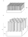
図1(A)は負極100の斜視図である。負極100が、活物質として機能する構造である。
FIG. 1A is a perspective view of the
ここで、活物質とは、キャリアイオンの吸蔵及び放出に関わる物質を指す。活物質層は、活物質の他に、導電助剤、バインダー、グラフェン等のいずれか一以上を有する。よって、活物質と活物質層は区別される。 Here, the active material refers to a substance related to insertion and extraction of carrier ions. The active material layer has one or more of a conductive additive, a binder, graphene, and the like in addition to the active material. Therefore, an active material and an active material layer are distinguished.
また、キャリアイオンとしてリチウムイオンを用いる二次電池をリチウム二次電池という。また、リチウムイオンの代わりに用いることが可能なキャリアイオンとしては、ナトリウムイオン、カリウムイオン等のアルカリ金属イオン、カルシウムイオン、ストロンチウムイオン、バリウムイオン等のアルカリ土類金属イオン、ベリリウムイオン、またはマグネシウムイオン等がある。 A secondary battery using lithium ions as carrier ions is called a lithium secondary battery. Carrier ions that can be used in place of lithium ions include alkali metal ions such as sodium ions and potassium ions, alkaline earth metal ions such as calcium ions, strontium ions, and barium ions, beryllium ions, or magnesium ions. Etc.
負極100の詳細な構造について、図1(B)、図2(A)及び図2(B)を用いて説明する。なお、負極100の代表的な形態を、図2(A)及び図2(B)において、それぞれ負極100a、100bとして説明する。
A detailed structure of the
図1(B)は負極100の拡大斜視図であり、図2(A)及び図2(B)は、負極100の拡大断面図である。負極100は、活物質101を有する。また、活物質101は、共通部101a、及び共通部101aから突出する柱状の突起101bを有する。図1(B)に示すように、柱状の突起101bは共通部101aの上面に複数が所定の間隔で配置される。この間隔は柱状の突起101bがキャリアイオンを吸蔵して体積膨張した際に、他の柱状の突起と接触しない程度に密に配置されるように設計する。このように活物質101に柱状の突起101bを複数設けることで、負極の表面積を大幅に増加させて充放電容量を向上させることができる。
1B is an enlarged perspective view of the
共通部101aは、柱状の突起101bの下地層として機能する。また、共通部101aは連続した層であり、共通部101a及び複数の柱状の突起101bは接している。なお、柱状の突起101bの頂部又は稜は湾曲していてもよい。湾曲すること、すなわち突起の端部に角部を持たないことで、キャリアイオンの脱挿入に伴う体積膨張収縮による角部への応力集中を緩和し、柱状の突起の変形を抑制することができる。
The
また、柱状の突起101bは、図1(A)、図1(B)においては突起の軸に垂直な断面形状は十字型である。この場合の断面形状とは、柱状の突起が形成された面と概略平行な平面を含む柱状の突起の断面の形状をいう。また柱状の突起101bは平坦な上面を有する。柱状の突起の上面に平坦な面を設けることで、後述するスペーサを用いた場合に、該スペーサと接触してスペーサを支持することが可能となる。このため、柱状の突起の上面の平坦性が高い程柱状の突起の座屈強度が高まり、また正極負極の間隔を一定かつ均一に保つことができ、蓄電装置の信頼性向上及び小型化に寄与する。なお、柱状の突起の上面の端部はその側面が湾曲していても良く、この場合には柱状の突起の上面の端部は平坦面とはならないことに留意する。
The
図1(A)、図1(B)においては、柱状の突起101bの断面形状を十字型で示す。しかし、突起の断面形状はこれに限られず、H字型、L字型、I字型、T字型、U字型、Z字型のような多角形状若しくは曲線を含む多角形状でも良く、またはこれらや十字型との組み合わせ等であっても良い。
1A and 1B, the cross-sectional shape of the
活物質101としては、キャリアであるイオンの吸蔵及び放出が可能なシリコン、ゲルマニウム、スズ、アルミニウム等のいずれか一以上を用いる。なお、活物質101として、充放電理論容量が高いシリコンを用いることが好ましい。または、リン、ボロン等の一導電型を付与する不純物元素が添加されたシリコンを用いてもよい。リン、ボロン等の一導電型を付与する不純物元素が添加されたシリコンは、導電性が高くなるため、負極の導電率を高めることができる。
As the
共通部101a及び複数の柱状の突起101bは適宜、単結晶構造または多結晶構造とすることができる。または、共通部101aを単結晶構造または多結晶構造とし、複数の柱状の突起101bを非晶質構造とすることができる。または、共通部101a及び複数の柱状の突起101bの一部を単結晶構造または多結晶構造とし、複数の柱状の突起101bの他部を非晶質構造とすることができる。なお、当該複数の柱状の突起101bの一部とは少なくとも共通部101aと接する領域を含む。
The
なお、共通部101a及び複数の柱状の突起101bの界面は明確でない。このため、活物質101において、複数の柱状の突起101bの間に形成される谷のうち最も深い谷の底を通り、且つ活物質101において、柱状の突起101bが形成される面と平行な面を、共通部101a及び複数の柱状の突起101bの界面104として定義する。
Note that the interface between the
また、複数の柱状の突起101bの長手方向は、揃っている。すなわち、複数の柱状の突起101bの軸105が揃っている。さらに好ましくは、複数の柱状の突起101bのそれぞれの形状が略同一である。このような構造とすることで、活物質の体積を制御することが可能である。なお、突起の軸105とは、突起の頂点(または上面の中心)と、突起が共通部と接する面の中心とを通る直線をいう。すなわち、柱状の突起の長手方向における中心を通る直線をいう。なお、複数の柱状突起の軸が揃っているとは、複数の柱状突起それぞれの当該直線が略一致する方向に平行になることをいい、代表的には、複数の柱状突起それぞれの軸でなす角度が10度以下、好ましくは5度以下である。
The longitudinal directions of the plurality of
なお、複数の柱状の突起101bが共通部101aから伸張している方向を長手方向と呼び、長手方向に切断した断面形状を長手方向の断面形状とよぶ。
A direction in which the plurality of
柱状の突起101bについて、突起の軸に垂直な断面形状における幅は、0.1μm以上1μm以下、好ましくは0.2μm以上0.5μm以下である。また、柱状の突起101bの高さは、突起の幅の5倍以上100倍以下、好ましくは10倍以上50倍以下であり、代表的には0.5μm以上100μm以下、好ましくは1μm以上50μm以下である。
The width of the
柱状の突起101bの突起の軸に垂直な断面形状における幅を、0.1μm以上とすることで、また、充放電容量を高めることが可能であり、1μm以下とすることで、充放電において突起が膨張しても、崩壊することを抑制することができる。また、柱状の突起101bの高さを、0.5μm以上とすることで、充放電容量を高めることが可能であり、100μm以下とすることで、充放電において突起が膨張しても、崩壊することを抑制することができる。
By setting the width in the cross-sectional shape perpendicular to the projection axis of the
なお、柱状の突起101bにおける「高さ」とは、長手方向の断面形状において、柱状の突起101bの頂点(または上面の中心)を通る軸に沿う方向の該頂点と共通部101aの間隔をいう。
The “height” in the
また、複数の柱状の突起101bはそれぞれ、一定の間隔を空けて共通部101a上に設けられる。柱状の突起101bの間隔は、柱状の突起101bの幅の1.29倍以上2倍以下とすることが好ましい。当該範囲は、後述するが、柱状の突起の上面の配置において、繰り返される基本構造の最小単位において、柱状の突起101bが占める割合を25%以上60%以下とすることが好ましいことに基づく。この結果、当該負極を用いた蓄電装置の充電により柱状の突起101bの体積が膨張しても、柱状の突起101bどうしが接触せず、柱状の突起101bの崩壊を抑制することができるとともに、蓄電装置の充放電容量の低下を妨げることができる。
Further, each of the plurality of
また、負極100の活物質101において共通部101aから複数の柱状の突起101bが突出しているため、板状の活物質に比べて表面積が広い。また、複数の柱状突起の軸が揃っており、さらに共通部に対して垂直方向に突出しているため、負極において突起の密度を高めることが可能であり、より表面積を増加させることができる。また、複数の柱状突起の間には隙間が設けられており、充電により活物質が膨張しても、突起どうしの接触を低減することが可能である。また後述するように、複数の柱状突起は並進対称性を有し、負極において均一性高く形成されているため、正極及び負極においての局所的な反応が低減し、キャリアイオン及び活物質の反応が正極及び負極の間で均質に生じる。これらのため、負極100を蓄電装置に用いた場合、高速な充放電が可能となるとともに、充放電による活物質の崩壊及び剥離を抑制でき、サイクル特性がさらに向上した蓄電装置を作製することができる。さらには、突起の形状を略一致することで、局所的な充放電を低減するとともに、活物質の重量を制御することが可能である。また、突起の高さが揃っていると、電池の作製工程時において局所的な荷重を防ぐことが可能であり、歩留まりを高めることができる。これらのため、電池の仕様を制御しやすい。
In addition, since the plurality of
また、図2(B)に示す負極100bのように、活物質101に含まれる複数の柱状の突起101bの上面に、保護層103を設けてもよい。
Further, as in the
保護層103は、導電層、半導体層、または絶縁層を適宜用いることができる。保護層103の厚さは100nm以上10μm以下が好ましい。なお、活物質101と比較してエッチング速度の遅い材料を用いて保護層103を形成することで、保護層103が複数の柱状突起をエッチングにより形成する際のハードマスクとして機能し、複数の柱状突起の高さのばらつきを低減することができる。
As the
本実施の形態に示す電極の断面形状について、図3を用いて説明する。 A cross-sectional shape of the electrode described in this embodiment is described with reference to FIGS.
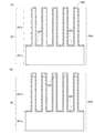
図3(A)は、共通部101aと、共通部101aから突出する複数の柱状の突起101bの上面図である。ここでは、突起の軸に垂直な断面形状が十字型である複数の柱状の突起101bが上下左右の方向に等間隔に配置されている。図3(A)乃至図3(C)においては、柱状の突起101bの断面形状を十字型で示す。しかし、突起の断面形状はこれに限られず、H字型、L字型、I字型、T字型、U字型、Z字型でも良く、またはこれらや十字型との組み合わせ等であっても良い。すなわち、断面形状が円形や楕円形ではなく、矩形形状を複数組み合わせた形状の多角形状若しくは曲線を含む多角形状である。
FIG. 3A is a top view of the
突起の軸に垂直な断面形状を円形にした場合、円は平面的に等方的な図形であるため、全方向(円を含む平面において、円の中心から円の外に向かう全ての方向。)の応力に対応できる。また加工も他の形状に比べて容易である。しかし、断面形状を円形にした場合、必要な機械的強度を確保するために断面形状の直径を大きくする必要がある。このため、断面形状をできるだけ小さくし、柱状の突起の密度を増加させて蓄電装置の大容量化を実現することに反する結果となる。一方で、断面形状を単純な矩形型にした場合には、方向性が生じて特定方向の応力にしか対応ができない構造耐力の低い構造となる。これに対して、柱状の突起の断面形状を、十字型、H字型、L字型、I字型、T字型、U字型、Z字型のような多角形状若しくは曲線を含む多角形状とすることで、水平応力に対して準等方的な安定構造となるため、断面形状の面積を大きくすることなく、全方向の応力に対応が可能な構造耐力を有することができる。このため、小さな突起を複数配置することができ、ひいては蓄電装置の容量を増大させることができる。 When the cross-sectional shape perpendicular to the axis of the protrusion is circular, the circle is a planar isotropic figure, so all directions (all directions from the center of the circle to the outside of the circle in the plane including the circle). ) Stress. Processing is also easier compared to other shapes. However, when the cross-sectional shape is circular, it is necessary to increase the diameter of the cross-sectional shape in order to ensure the necessary mechanical strength. For this reason, the cross-sectional shape is made as small as possible and the density of the columnar protrusions is increased, which is contrary to the realization of an increase in the capacity of the power storage device. On the other hand, when the cross-sectional shape is a simple rectangular shape, a structure with low structural yield strength that can handle only stress in a specific direction is generated. On the other hand, the cross-sectional shape of the columnar protrusion is a polygonal shape including a cross shape, an H shape, an L shape, an I shape, a T shape, a U shape, a Z shape, or a curved shape. By doing so, a quasi-isotropic stable structure with respect to horizontal stress is obtained, so that it is possible to have structural strength capable of dealing with stress in all directions without increasing the cross-sectional area. For this reason, a plurality of small protrusions can be provided, and as a result, the capacity of the power storage device can be increased.
また、断面形状を十字型等の形状にした場合、円形にした場合と比較して、柱状の突起における体積当たりの表面積が増大する。このため、断面形状を十字型等の多角形状若しくは曲線を含む多角形状とする突起を形成することで、蓄電装置の高出力化が可能となる。 In addition, when the cross-sectional shape is a cross shape or the like, the surface area per volume of the columnar protrusion is increased as compared with a circular shape. For this reason, it is possible to increase the output of the power storage device by forming protrusions whose cross-sectional shape is a polygonal shape such as a cross or a polygonal shape including a curve.
図3(B)は、図3(A)を方向aに移動したときの断面図である。図3(A)及び図3(B)おいて、複数の柱状の突起101bの位置が同一である。また、ここでは、図3(A)において、方向aに移動したが、方向b、方向cにそれぞれ移動しても、図3(B)と同様の配置となる。すなわち、図3(A)に示す複数の柱状の突起101bは柱状の突起の断面が並ぶ平面座標において、並進操作において所定の距離をとっても対称である並進対称性を有する。また、図3(A)に示す複数の柱状の突起101bは、例えば十字型の断面形状の中心を軸に90°回転した場合もとの断面形状に重なるため回転対称性を有する。
FIG. 3B is a cross-sectional view when FIG. 3A is moved in the direction a. 3A and 3B, the positions of the plurality of
ここで、図3(A)の柱状の突起の断面の配置において、繰り返される基本構造の最小単位(以下、対称性の単位という)を破線110で示す。対称性の単位において、柱状の突起101bが占める割合は、25%以上60%以下が好ましい。すなわち、対称性の単位における柱状の突起間の空隙率は40%以上75%以下であることが好ましい。対称性の単位において、柱状の突起101bの占める割合を25%以上とすると、負極における充放電の理論容量を約1000mAh/g以上とすることができる。一方、柱状の突起101bが占める割合を60%とすることで、充放電容量が最大(すなわち、理論容量)となり、隣り合う突起が膨張しても突起どうしが接触せず、突起の崩壊を防ぐことができる。この結果、高い充放電容量を達成するとともに、充放電による負極の劣化を低減することができる。
Here, in the arrangement of the cross-sections of the columnar protrusions in FIG. 3A, a minimum unit (hereinafter referred to as a symmetry unit) of the basic structure that is repeated is indicated by a
図3(A)に示す、柱状の突起101bが占める割合は約31%である。これに対して、図3(C)では、十字型の断面形状の柱状の突起を所定の方向において千鳥状(ジグザグ状)になるように配置されている。この場合には、柱状の突起101bが占める割合は約50%であり、図3(A)に示す柱状の突起の配置と比べて、充放電の理論容量を増加させることができる。
The proportion of the
また、図4(A)乃至図4(D)は、柱状の突起の軸に垂直な断面形状について、十字型以外の形状の例を示すものである。図4(A)は、柱状の突起の断面形状が、U字型であるものを示す図である。図4(B)は、柱状の突起の断面形状が、H字型又はI字型であるものを示す図である。図4(C)は、柱状の突起の断面形状が、L字型であるものを示す図である。図4(D)は、柱状の突起の断面形状が、T字型であるものを示す図である。図4(A)乃至図4(D)に示す柱状の突起の断面形状は、いずれも複数の矩形を合わせた図形であり、それら図形の配置は並進対称性を有する。 4A to 4D show examples of cross-sectional shapes other than the cross shape perpendicular to the axis of the columnar protrusion. FIG. 4A is a diagram showing a columnar protrusion having a U-shaped cross-sectional shape. FIG. 4B is a diagram illustrating a columnar protrusion whose cross-sectional shape is H-shaped or I-shaped. FIG. 4C is a diagram showing a columnar protrusion having an L-shaped cross section. FIG. 4D is a diagram showing a columnar protrusion having a T-shaped cross section. Each of the cross-sectional shapes of the columnar protrusions shown in FIGS. 4A to 4D is a figure formed by combining a plurality of rectangles, and the arrangement of these figures has translational symmetry.
複数の柱状の突起を並進対称性に配置することで、複数の柱状の突起それぞれの電子伝導性のばらつきを低減することができる。このため、正極及び負極においての局所的な反応が低減され、キャリアイオン及び活物質の反応が均一に生じ、拡散過電圧(濃度過電圧)を防ぐとともに、電池特性の信頼性を高めることができる。 By arranging the plurality of columnar protrusions in translational symmetry, variations in the electron conductivity of each of the plurality of columnar protrusions can be reduced. For this reason, the local reaction in the positive electrode and the negative electrode is reduced, the reaction between the carrier ions and the active material occurs uniformly, preventing diffusion overvoltage (concentration overvoltage) and improving the reliability of battery characteristics.
また、図4(A)乃至図4(D)に示す断面形状は、全方向の応力に対応することが可能な構造である。これにより、負極の機械的強度が向上する。また、断面形状を千鳥状(ジグザグ状)に配置しているため、強度をさらに向上させることに寄与している。 In addition, the cross-sectional shapes illustrated in FIGS. 4A to 4D are structures that can handle stress in all directions. Thereby, the mechanical strength of the negative electrode is improved. Moreover, since the cross-sectional shape is arranged in a zigzag shape (zigzag shape), it contributes to further improving the strength.
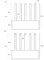
次に、負極100の作製方法について図5を用いて説明する。ここでは、負極100の一形態として、図2(A)に示す負極100aを用いて説明する。
Next, a method for manufacturing the
図5(A)に示すように、シリコン基板120上にマスク121を形成する。
As shown in FIG. 5A, a
シリコン基板120は、単結晶シリコン基板または多結晶シリコン基板を用いる。なお、シリコン基板は、リンが添加されたn型シリコン基板、ボロンが添加されたp型シリコン基板を用いることで、集電体を設けずとも、活物質を負極として用いることができる。
As the
マスク121は、フォトリソグラフィ工程により形成することができる。また、マスク121は、インクジェット法、印刷法等を用いて形成することができる。マスク121の上面パターンは、図3又は図4で示すような、十字型等の図形を所定の間隔で配列させたパターンを用いる。
The
次に、マスク121を用いて、シリコン基板120を選択的にエッチングして、図5(B)に示すように、共通部101a及び複数の柱状の突起101bを有する活物質101を形成する。シリコン基板のエッチング方法としては、ドライエッチング法、ウエットエッチング法を適宜用いることができる。なお、深堀りエッチング法であるボッシュ法を用いることで、高さの高い突起を形成することができる。
Next, the
例えば、ICP(Inductively Coupled Plasma:誘導結合型プラズマ)装置を用い、エッチングガスとして塩素、臭化水素、及び酸素を用いて、n型のシリコン基板をエッチングすることで、共通部101a及び複数の柱状の突起101bを有する活物質101を形成することができる。なお、ここでは、共通部101aが残存するように、エッチング時間を調整する。また、エッチングガスの流量比は適宜調整すればよいが、エッチングガスの流量比の一例として、塩素、臭化水素、及び酸素それぞれの流量比を10:15:3とすることができる。
For example, by using an ICP (Inductively Coupled Plasma) apparatus and etching an n-type silicon substrate using chlorine, hydrogen bromide, and oxygen as etching gases, the
本実施の形態に示すように、マスクを用いてシリコン基板をエッチングすることで、軸が揃っている複数の柱状突起を形成することができる。また、断面形状を十字型等の任意の形状とする柱状の突起を形成することができる。さらには、立体形状が略一致している複数の柱状の突起を形成することができる。 As shown in this embodiment mode, a plurality of columnar protrusions with aligned axes can be formed by etching a silicon substrate using a mask. In addition, columnar protrusions having an arbitrary shape such as a cross shape can be formed. Furthermore, it is possible to form a plurality of columnar protrusions having substantially the same three-dimensional shape.
最後に、マスク121を除去することで、図5(C)に示すように、負極100aを作製することができる。
Finally, by removing the
本実施の形態により、図2(A)に示す負極100aを形成することができる。
According to this embodiment, the
なお、シリコン基板120上に保護層を形成し、当該保護層上にマスク121を形成し、当該マスク121を用いて、分離された保護層103(図2(B)参照。)を形成した後、当該マスク121及び分離された保護層を用いてシリコン基板120を選択的にエッチングすることで、図2(B)に示す負極100bを形成することができる。このとき、複数の柱状の突起101bの高さが高い場合、即ちエッチング時間が長い場合、エッチング工程においてマスクの厚さが徐々に薄くなり、一部のマスクが除去され、シリコン基板120が露出されてしまう。この結果、突起の高さにばらつきが生じるが、分離された保護層103をハードマスクとして用いることで、シリコン基板120の露出を妨げることが可能であり、突起の高さのばらつきを低減することができる。
Note that after a protective layer is formed over the
(実施の形態2)
本実施の形態では、充放電による劣化が少なく、高充放電サイクル特性を有する蓄電装置の負極の構造及びその作製方法について、図6乃至図7を用いて説明する。本実施の形態で説明する負極は、実施の形態1と比較して、グラフェンを設ける構成を有する点において異なる。
(Embodiment 2)
In this embodiment, a structure and a manufacturing method of a negative electrode of a power storage device with little deterioration due to charge and discharge and high charge / discharge cycle characteristics will be described with reference to FIGS. The negative electrode described in this embodiment is different from that in
図6(A)は負極200の斜視図である。負極200が、活物質として機能する構造である。
FIG. 6A is a perspective view of the
負極200の詳細な構造について、図6(B)、図7(A)及び図7(B)を用いて説明する。なお、負極200の代表的な形態を、図7(A)及び図7(B)において、それぞれ負極200a、200bとして説明する。
A detailed structure of the
本実施の形態に示す負極200は、実施の形態1で示した負極100の表面がグラフェン202で覆われたものである。すなわち、負極200は、活物質201、及び活物質201を覆うグラフェン202を有する。その他の構成は柱状の突起の断面形状も含めて、実施の形態1で示した負極100と同様である。
In the
グラフェン202は、共通部201aの上面、柱状の突起201bの側面及び上面を覆う。グラフェンは活物質の各部分と直接接していても良く、また、キャリアイオンの活物質への脱挿入が可能な程度において、活物質とグラフェンとの間に酸化膜等の絶縁膜が存在することも許容される。
The
グラフェン202は、導電助剤として機能する。また、グラフェン202は、活物質として機能する場合もある。
The
グラフェン202は、単層グラフェンまたは多層グラフェンを含む。グラフェン202は、長さが数μmのシート状である。
The
単層グラフェンは、π結合を有する1原子層の炭素分子のシートのことをいい、極めて厚さが薄い。また、炭素で構成される六員環が平面方向に広がっており、七員環、八員環、九員環、十員環等の、六員環の一部の炭素結合が切断された多員環が一部に形成される。 Single layer graphene refers to a sheet of monoatomic carbon molecules having a π bond and is extremely thin. In addition, a six-membered ring made of carbon spreads in the plane direction, and many carbon bonds in the six-membered ring such as seven-membered ring, eight-membered ring, nine-membered ring, and ten-membered ring are broken. A member ring is formed in part.
なお、多員環は、炭素及び酸素で構成される場合がある。または、多員環の炭素に酸素が結合する場合がある。グラフェンに酸素を含む場合、六員環の一部の炭素結合が切断され、結合が切断された炭素に酸素が結合し、多員環が形成される。このため、当該炭素及び酸素の結合の内部には、イオンの移動が可能な通路として機能する間隙を有する。すなわち、グラフェンに含まれる酸素の割合が多いほど、イオンの移動が可能な通路である間隙の割合が増加する。 The multi-membered ring may be composed of carbon and oxygen. Alternatively, oxygen may be bonded to carbon of a multi-membered ring. In the case where graphene contains oxygen, part of the carbon bond of the six-membered ring is broken, and oxygen is bonded to the carbon whose bond is broken, thereby forming a multi-membered ring. For this reason, a gap functioning as a passage through which ions can move is formed inside the carbon-oxygen bond. That is, the greater the proportion of oxygen contained in graphene, the greater the proportion of gaps that are channels through which ions can move.
なお、グラフェン202に酸素が含まれる場合、酸素の割合は全体の2atomic%以上11atomic%以下、好ましくは3atomic%以上10atomic%以下である。酸素の割合が低い程、グラフェンの導電性を高めることができる。また、酸素の割合を高める程、グラフェンにおいてイオンの通路となる間隙をより多く形成することができる。
Note that in the case where oxygen is contained in the
グラフェン202が多層グラフェンの場合、複数の単層グラフェンで構成され、代表的には、単層グラフェンが2層以上100層以下で構成されるため、極めて厚さが薄い。単層グラフェンが酸素を有することで、グラフェンの層間距離は0.34nmより大きく0.5nm以下、好ましくは0.38nm以上0.42nm以下、更に好ましくは0.39nm以上0.41nm以下となる。通常のグラファイトは、単層グラフェンの層間距離が0.34nmであり、グラフェン202の方がグラファイトよりも層間距離が長いため、単層グラフェンの表面と平行な方向におけるイオンの移動が容易となる。また、酸素を含み、多員環が構成される単層グラフェンまたは多層グラフェンで構成され、所々に間隙を有する。このため、グラフェン202が多層グラフェンの場合、単層グラフェンの表面と平行な方向、即ち単層グラフェンどうしの隙間とともに、グラフェンの表面に対する垂直方向、即ち単層グラフェンそれぞれに設けられる間隙の間をイオンが移動することが可能である。
In the case where the
負極の活物質として、シリコンを用いることで、グラファイトを活物質として用いた場合と比較して、理論吸蔵容量が大きいため、蓄電装置の小型化に有利である。 By using silicon as the active material for the negative electrode, the theoretical storage capacity is larger than when graphite is used as the active material, which is advantageous for downsizing the power storage device.
また、負極200の活物質201において共通部201aから複数の柱状の突起201bが突出しているため、板状の活物質に比べて表面積が広い。また、複数の柱状突起の軸が揃っており、さらに共通部に対して垂直方向に突出しているため、負極において突起の密度を高めることが可能であり、より表面積を増加させることができる。また、複数の柱状突起の間には隙間が設けられており、さらに、活物質をグラフェンが覆うため、充電により活物質が膨張しても、突起どうしの接触を低減することが可能である。さらに、活物質が剥離してもグラフェンにより、活物質の崩落を防ぐことができる。また、複数の柱状の突起は並進対称性を有し、負極において均一性高く形成されているため、正極及び負極においての局所的な反応が低減し、キャリアイオン及び活物質の反応が正極及び負極の間で均質に生じる。これらのため、負極200を蓄電装置に用いた場合、高速な充放電が可能となるとともに、充放電による活物質の崩壊及び剥離を抑制でき、サイクル特性がさらに向上した蓄電装置を作製することができる。さらには、突起の形状を略一致することで、局所的な充放電を低減するとともに、活物質の重量を制御することが可能である。また、突起の高さが揃っていると、電池の作製工程時において局所的な荷重を防ぐことが可能であり、歩留まりを高めることができる。これらのため、電池の仕様を制御しやすい。
Further, in the
また、蓄電装置において、活物質201表面が電解質と接触することにより、電解質及び活物質が反応し、活物質の表面に被膜が形成される。当該被膜はSEI(Solid Electrolyte Interface)と呼ばれ、活物質と電解質の反応を緩和し、安定化させるために必要であると考えられている。しかしながら、当該被膜が厚くなると、キャリアイオンが活物質に吸蔵されにくくなり、活物質と電解質間のキャリアイオン伝導性の低下などの問題がある。
Further, in the power storage device, when the surface of the
活物質201をグラフェン202で被覆することで、当該被膜の膜厚の増加を抑制することが可能であり、キャリアイオン伝導性の低下を抑制することができる。
By coating the
また、グラフェンは導電性が高いため、シリコンをグラフェンで被覆することで、グラフェンにおいて電子の移動を十分速くすることができる。また、グラフェンは厚さの薄いシート状であるため、複数の柱状突起上にグラフェンを設けることで、活物質層に含まれる活物質量をより多くすることが可能であるとともに、キャリアイオンの移動がグラファイトより容易となる。これらの結果、キャリアイオンの伝導性を高めることができ、活物質であるシリコン及びキャリアイオンの反応性を高めることが可能であり、キャリアイオンが活物質に吸蔵されやすくなる。このため、当該負極を用いた蓄電装置において、急速充放電が可能である。 In addition, since graphene has high conductivity, the movement of electrons can be sufficiently accelerated in graphene by covering silicon with graphene. In addition, since graphene is a thin sheet, it is possible to increase the amount of active material contained in the active material layer and to move carrier ions by providing graphene on a plurality of columnar protrusions. Is easier than graphite. As a result, the conductivity of carrier ions can be increased, the reactivity of silicon as an active material and carrier ions can be increased, and carrier ions can be easily stored in the active material. For this reason, in the power storage device using the negative electrode, rapid charging / discharging is possible.
なお、活物質201とグラフェン202の間に、酸化シリコン層を有してもよい。活物質201上に酸化シリコン層を設けることで、蓄電装置の充電時に酸化シリコン中にキャリアであるイオンが挿入される。この結果、Li4SiO4、Na4SiO4、K4SiO4等のアルカリ金属シリケート、Ca2SiO4、Sr2SiO4、Ba2SiO4等のアルカリ土類金属シリケート、Be2SiO4、Mg2SiO4等のシリケート化合物が形成される。これらのシリケート化合物は、キャリアイオンの移動パスとして機能する。また、酸化シリコン層を有することで、活物質201の膨張を抑制することができる。これらのため、充放電容量を維持しつつ、活物質201の崩壊を抑えることができる。なお、充電の後、放電しても、酸化シリコン層において形成されたシリケート化合物から、キャリアイオンとなる金属イオンは全て放出されず、一部残存するため、酸化シリコン層は、酸化シリコン及びシリケート化合物の混合層となる。
Note that a silicon oxide layer may be provided between the
また、当該酸化シリコン層の厚さを2nm以上10nm以下とすることが好ましい。酸化シリコン層の厚さを2nm以上とすることで、充放電による活物質201の膨張を緩和することができる。また、酸化シリコン層の厚さ10nm以下であると、キャリアとなるイオンの移動が容易であり、充放電容量の低下を妨げることができる。酸化シリコン層を活物質201上に設けることで、充放電における活物質201の膨張及び収縮を緩和し、活物質201の崩壊を抑制することができる。
The thickness of the silicon oxide layer is preferably 2 nm or more and 10 nm or less. By setting the thickness of the silicon oxide layer to 2 nm or more, expansion of the
また、図7(B)に示す負極200bのように、活物質201に含まれる複数の柱状の突起201bの頂部及びグラフェン202の間に、保護層203を設けてもよい。
Further, as in the
保護層203は、導電層、半導体層、または絶縁層を適宜用いることができる。保護層203の厚さは100nm以上10μm以下が好ましい。なお、活物質201と比較してエッチング速度の遅い材料を用いて保護層203を形成することで、保護層203が複数の柱状突起をエッチングにより形成する際のハードマスクとして機能し、複数の柱状突起の高さのばらつきを低減することができる。
As the
次に、負極200の作製方法について説明する。複数の柱状の突起を有する活物質を形成する工程までは、実施の形態1で示した作製方法と同様である。
Next, a method for manufacturing the
活物質201上にグラフェン202を形成することで、図7(A)に示すように、負極200aを作製することができる。
By forming the
グラフェン202の形成方法としては、活物質201上にニッケル、鉄、金、銅またはそれらを含む合金を核として形成した後、メタンまたはアセチレン等の炭化水素を含む雰囲気で核からグラフェンを成長させる気相法がある。また、酸化グラフェンを含む分散液を用いて、活物質201の表面に酸化グラフェン設けた後、酸化グラフェンを還元し、グラフェンとする液相法がある。
As a method for forming the
酸化グラフェンを含む分散液は、酸化グラフェンを溶媒に分散させる方法、溶媒中でグラファイトを酸化した後、酸化グラファイトを酸化グラフェンに分離して、酸化グラフェンを含む分散液を形成する方法等により得ることができる。ここでは、グラファイトを酸化した後、酸化グラファイトを酸化グラフェンに分離して形成した酸化グラフェンを含む分散液を用いて、活物質201上にグラフェン202を形成する方法について、説明する。
A dispersion containing graphene oxide is obtained by a method of dispersing graphene oxide in a solvent, a method of oxidizing graphite in a solvent, then separating the graphite oxide into graphene oxide, and forming a dispersion containing graphene oxide. Can do. Here, a method for forming the
本実施の形態では、Hummers法と呼ばれる酸化法を用いて酸化グラフェンを形成する。Hummers法は、単結晶グラファイト粉末に過マンガン酸カリウムの硫酸溶液、過酸化水素水等を加えて酸化反応させて酸化グラファイトを含む混合液を形成する。酸化グラファイトは、グラファイトの炭素の酸化により、カルボキシル基等のカルボニル基、ヒドロキシル基等の官能基を有する。このため、複数のグラフェンの層間距離がグラファイトと比較して長い。次に、酸化グラファイトを含む混合液に超音波振動を加えることで、層間距離の長い酸化グラファイトを劈開し、酸化グラフェンを分離することができるとともに、酸化グラフェンを含む分散液を形成することができる。なお、Hummers法以外の酸化グラフェンの形成方法を適宜用いることができる。 In this embodiment, graphene oxide is formed using an oxidation method called a Hummers method. In the Hummers method, a mixed solution containing graphite oxide is formed by adding a sulfuric acid solution of potassium permanganate, a hydrogen peroxide solution or the like to single crystal graphite powder to cause an oxidation reaction. Graphite oxide has a functional group such as a carbonyl group such as a carboxyl group and a hydroxyl group by oxidation of carbon of graphite. For this reason, the interlayer distance of a plurality of graphenes is longer than that of graphite. Next, by applying ultrasonic vibration to the mixed liquid containing graphite oxide, it is possible to cleave graphite oxide having a long interlayer distance to separate graphene oxide and to form a dispersion liquid containing graphene oxide. . Note that a method for forming graphene oxide other than the Hummers method can be used as appropriate.
なお、酸化グラフェンは、エポキシ基、カルボキシル基等のカルボニル基、ヒドロキシル基等を有する。なお、カルボニル基を有する酸化グラフェンは極性を有する液体中において水素が電離するため、酸化グラフェンはイオン化し、異なる酸化グラフェンどうしが凝集しにくい。このため、極性を有する液体においては、均一に酸化グラフェンが分散するとともに、後の工程において、酸化シリコン層の表面に均一な割合で酸化グラフェンを設けることができる。 Note that graphene oxide has an epoxy group, a carbonyl group such as a carboxyl group, a hydroxyl group, and the like. Note that in graphene oxide having a carbonyl group, hydrogen is ionized in a polar liquid, so that graphene oxide is ionized and different graphene oxides are less likely to aggregate. Therefore, in the liquid having polarity, the graphene oxide is uniformly dispersed, and the graphene oxide can be provided at a uniform ratio on the surface of the silicon oxide layer in a later step.
酸化グラフェンを含む分散液に活物質201を浸し、活物質201上に酸化グラフェンを設ける方法としては、塗布法、スピンコート法、ディップ法、スプレー法、電気泳動法等がある。また、これらの方法を複数組み合わせてもよい。なお、電気泳動法を用いると、イオン化した酸化グラフェンを電気的に活物質まで移動させることができるため、共通部及び複数の柱状突起の接する領域にまで酸化グラフェンを設けることが可能である。このため、複数の柱状突起の高さが高い場合でも、共通部及び複数の柱状突起の表面に均一に酸化グラフェン設けることができる。
As a method for immersing the
活物質201上に設けられた酸化グラフェンを還元する方法としては、真空中あるいは不活性ガス(窒素あるいは希ガス等)中等の雰囲気で、150℃以上、好ましくは200℃以上の温度、活物質201が耐えうる温度以下で加熱する方法がある。加熱する温度が高い程、また、加熱する時間が長いほど、酸化グラフェンが還元されやすく、純度の高い(すなわち、炭素以外の元素の濃度の低い)グラフェンが得られる。または、還元性溶液に浸し、酸化グラフェンを還元する方法がある。
As a method for reducing graphene oxide provided on the
なお、Hummers法では、グラファイトを硫酸で処理するため、酸化グラファイトは、スルホン基等も結合しているが、この分解(脱離)は、300℃前後で開始する。したがって、加熱により酸化グラフェンを還元する方法において、酸化グラフェンの還元は300℃以上で行うことが好ましい。 In the Hummers method, since graphite is treated with sulfuric acid, graphite oxide is also bonded with a sulfone group and the like, but this decomposition (desorption) starts at around 300 ° C. Therefore, in the method of reducing graphene oxide by heating, the reduction of graphene oxide is preferably performed at 300 ° C. or higher.
上記還元処理において、隣接するグラフェンどうしが結合し、より巨大な網目状あるはシート状となる。また、当該還元処理において、酸素の脱離により、グラフェン内には間隙が形成される。更には、グラフェンどうしが基体の表面に対して、平行に重なり合う。この結果、グラフェンの層間及びグラフェン内の間隙においてイオンの移動が可能なグラフェンが形成される。 In the above reduction treatment, adjacent graphenes are combined to form a larger network or sheet. In the reduction treatment, a gap is formed in the graphene due to desorption of oxygen. Furthermore, the graphenes overlap in parallel with the surface of the substrate. As a result, graphene capable of ion migration is formed between the graphene layers and in the gaps in the graphene.
本実施の形態により、図7(A)に示す負極200aを形成することができる。
According to this embodiment, the
(実施の形態3)
本実施の形態では、充放電による劣化が少なく、高充放電サイクル特性を有する蓄電装置の負極の構造及びその作製方法について、図8を用いて説明する。本実施の形態で説明する負極は、実施の形態1と比較して、集電体を有する構成で異なり、さらにグラフェンを設けた構成も説明する。
(Embodiment 3)
In this embodiment, a structure and a manufacturing method of a negative electrode of a power storage device with less deterioration due to charge and discharge and high charge / discharge cycle characteristics will be described with reference to FIGS. The negative electrode described in this embodiment is different from that in
図8(A)及び図8(B)は負極300の俯瞰図である。負極300は、集電体303上に活物質層が設けられる。
8A and 8B are overhead views of the
図8(B)は、集電体303及び活物質層の拡大断面図である。集電体303上に活物質層が設けられる。また、活物質層は、活物質301及び活物質301を覆うグラフェン302を有する。また、活物質301は、共通部301a、及び共通部301aから突出する複数の柱状の突起301bを有する。また、複数の柱状の突起301bの長手方向は、揃っている。すなわち、複数の柱状の突起301bの軸が揃っている。
FIG. 8B is an enlarged cross-sectional view of the
集電体303は、ステンレス、金、白金、亜鉛、鉄、アルミニウム、銅、チタン等に代表される金属、及びこれらの合金など、導電性の高い材料を用いることができる。なお、集電体303として、シリコン、チタン、ネオジム、スカンジウム、モリブデンなどの耐熱性を向上させる元素が添加されたアルミニウム合金を用いることが好ましい。また、集電体303として、シリコンと反応してシリサイドを形成する金属元素で形成してもよい。シリコンと反応してシリサイドを形成する金属元素としては、ジルコニウム、チタン、ハフニウム、バナジウム、ニオブ、タンタル、クロム、モリブデン、タングステン、コバルト、ニッケル等がある。
The
集電体303は、箔状、板状(シート状)、網状、パンチングメタル状、エキスパンドメタル状等の形状を適宜用いることができる。
The
活物質301は、実施の形態1に示す活物質101と同様の材料を適宜用いることができる。
As the
共通部301aは、実施の形態1に示す共通部101aと同様に、複数の柱状の突起301bの下地層として機能し、集電体303上に連続している層である。また、共通部301a及び複数の柱状の突起301bは接している。
The
複数の柱状の突起301bは、実施の形態1に示す複数の柱状の突起101bの形状を適宜用いることができる。
As the plurality of
共通部301a及び複数の柱状の突起301bは適宜、単結晶構造、多結晶構造、または非晶質構造とすることができる。また、微結晶構造等、これらの中間に位置する結晶構造とすることができる。さらに、共通部301aを単結晶構造または多結晶構造とし、複数の柱状の突起301bを非晶質構造とすることができる。または、共通部301a及び複数の柱状の突起301bの一部を単結晶構造または多結晶構造とし、複数の柱状の突起301bの他部を非晶質構造とすることができる。なお、当該複数の柱状の突起301bの一部とは少なくとも共通部301aと接する領域を含む。
The
複数の柱状の突起301bの幅及び高さは、実施の形態1に示す柱状の突起101bと同様にすることができる。
The width and height of the plurality of
グラフェン302は、実施の形態2に示すグラフェン202と同様の構造を適宜用いることができる。
As the
なお、図示しないが、活物質は共通部を有さずに、集電体303上に分離された複数の柱状の突起301bが設けられ、集電体303及び複数の柱状の突起301b上にグラフェン302が形成されてもよい。また、複数の柱状の突起301bの軸は、揃っている。
Note that although not illustrated, the active material does not have a common portion, and a plurality of
この場合、グラフェン302は集電体303の一部と接するため、グラフェン302において電子が流れやすくなり、キャリアイオン及び活物質の反応性を高めることができる。
In this case, since the
また、集電体303としてシリサイドを形成する金属材料を用いる場合、集電体303において、活物質301と接する側にシリサイド層が形成される場合がある。集電体303にシリサイドを形成する金属材料を用いると、チタンシリサイド、ジルコニウムシリサイド、ハフニウムシリサイド、バナジウムシリサイド、ニオブシリサイド、タンタルシリサイド、クロムシリサイド、モリブデンシリサイド、コバルシリサイド、ニッケルシリサイド等がシリサイド層として形成される。
In the case where a metal material that forms silicide is used as the
本実施の形態に示す負極は、集電体303を支持体として活物質層を設けることができる。このため、集電体303が箔状、網状等の可撓性を有する場合、可撓性を有する負極を作製することができる。
In the negative electrode described in this embodiment, an active material layer can be provided using the
次に、負極300の作製方法については、実施の形態1に示す方法と同様であるが、本実施の形態においては、集電体303上にシリコン層を形成し、エッチング工程を行って共通部301aと柱状の突起301bを有する活物質301を形成する点において異なる。
Next, a method for manufacturing the
具体的な負極300の作製方法を、図9を用いて以下に説明する。まず、集電体303上にシリコン層320を形成する。次に、シリコン層320に、実施の形態1と同様に、マスク321を形成する。
A specific method for manufacturing the
シリコン層320は、CVD法、スパッタリング法、蒸着法等を適宜用いることができる。シリコン層320としては、単結晶シリコン、多結晶シリコン、または非晶質シリコンを用いて形成する。なお、シリコン層320は、リンが添加されたn型シリコン層、ボロンが添加されたp型シリコン層としてもよい。
For the
次に、マスク321を用いて、シリコン層320を選択的にエッチングして、図9(B)に示すように、共通部301a及び複数の柱状の突起301bを有する活物質301を形成する。シリコン層320のエッチング方法としては、ドライエッチング法、ウエットエッチング法を適宜用いることができる。なお、ドライエッチング法でも、ボッシュ法を用いることで、高さの高い突起を形成することができる。
Next, the
次に、マスク321を除去した後に、活物質301上に、グラフェン302を形成することで、集電体303上に活物質層を有する負極300を作製することができる。
Next, after removing the
グラフェン302は、実施の形態2に示すグラフェン202と同様に形成することができる。
The
なお、図9(B)において、共通部301aをエッチングし、集電体303を露出させることで、集電体上に柱状の突起301bのみを活物質として有する負極を作製することもできる。
Note that in FIG. 9B, the
また、シリコン層320上に保護層(図示せず)を形成し、当該保護層上にマスク321を形成し、当該マスク321を用いて、分離された保護層(図7(B)参照。)を形成した後、当該マスク321及び分離された保護層を用いてシリコン層320を選択的にエッチングすることで、保護層を有する活物質層を有する負極を作製することができる。このとき、複数の柱状の突起301bの高さが高い場合、即ちエッチング時間が長い場合、エッチング工程においてマスクの厚さが徐々に薄くなり、一部のマスクが除去され、シリコン層320が露出されてしまう。この結果、突起の高さにばらつきが生じるが、分離された保護層をハードマスクとして用いることで、シリコン層320の露出を妨げることが可能であり、突起の高さのばらつきを低減することができる。
Further, a protective layer (not shown) is formed over the
(実施の形態4)
本実施の形態では、蓄電装置の正極構造及び作製方法について説明する。
(Embodiment 4)
In this embodiment, a positive electrode structure and a manufacturing method of a power storage device will be described.
図10(A)は正極400の断面図である。正極400は、正極集電体401上に正極活物質層402が形成される。
FIG. 10A is a cross-sectional view of the
正極集電体401は、白金、アルミニウム、銅、チタン、ステンレス等の導電性の高い材料を用いることができる。また、正極集電体401は、箔状、板状、網状等の形状を適宜用いることができる。
The positive electrode
正極活物質層402は、LiFeO2、LiCoO2、LiNiO2、LiMn2O4、V2O5、Cr2O5、MnO2等の材料として用いることができる。
The positive electrode
または、オリビン型構造のリチウム含有複合酸化物(一般式LiMPO4(Mは、Fe(II),Mn(II),Co(II),Ni(II)の一以上)を用いることができる。一般式LiMPO4の代表例としては、LiFePO4、LiNiPO4、LiCoPO4、LiMnPO4、LiFeaNibPO4、LiFeaCobPO4、LiFeaMnbPO4、LiNiaCobPO4、LiNiaMnbPO4(a+bは1以下、0<a<1、0<b<1)、LiFecNidCoePO4、LiFecNidMnePO4、LiNicCodMnePO4(c+d+eは1以下、0<c<1、0<d<1、0<e<1)、LiFefNigCohMniPO4(f+g+h+iは1以下、0<f<1、0<g<1、0<h<1、0<i<1)等のリチウム化合物を材料として用いることができる。
Alternatively, a lithium-containing composite oxide having a olivine structure (general formula LiMPO 4 (M is one or more of Fe (II), Mn (II), Co (II), Ni (II)) can be used. Representative examples of the formula LiMPO 4 include LiFePO 4 , LiNiPO 4 , LiCoPO 4 , LiMnPO 4 , LiFe a Ni b PO 4 , LiFe a Co b PO 4 , LiFe a Mn b PO 4 , LiNi a Co b PO 4 . a Mn b PO 4 (a + b ≦ 1, 0 <a <1,0 <b <1), LiFe c Ni d
または、一般式Li(2−j)MSiO4(Mは、Fe(II),Mn(II),Co(II),Ni(II)の一以上、0≦j≦2)等のリチウム含有複合酸化物を用いることができる。一般式Li(2−j)MSiO4の代表例としては、Li(2−j)FeSiO4、Li(2−j)NiSiO4、Li(2−j)CoSiO4、Li(2−j)MnSiO4、Li(2−j)FeaNibSiO4、Li(2−j)FeaCobSiO4、Li(2−j)FekMnlSiO4、Li(2−j)NikColSiO4、Li(2−j)NikMnlSiO4(k+lは1以下、0<k<1、0<l<1)、Li(2−j)FemNinCoqSiO4、Li(2−j)FemNinMnqSiO4、Li(2−j)NimConMnqSiO4(m+n+qは1以下、0<m<1、0<n<1、0<q<1)、Li(2−j)FerNisCotMnuSiO4(r+s+t+uは1以下、0<r<1、0<s<1、0<t<1、0<u<1)等のリチウム化合物を材料として用いることができる。
Or a lithium-containing composite such as a general formula Li (2-j) MSiO 4 (M is one or more of Fe (II), Mn (II), Co (II), Ni (II), 0 ≦ j ≦ 2) An oxide can be used. Representative examples of the general formula Li (2-j) MSiO 4 include Li (2-j) FeSiO 4 , Li (2-j) NiSiO 4 , Li (2-j) CoSiO 4 , Li (2-j) MnSiO 4 , Li (2-j) Fe a Ni b SiO 4 , Li (2-j) Fe a Co b SiO 4 , Li (2-j) Fe k Mn l SiO 4 , Li (2-j) Ni k Co l SiO 4, Li (2- j) Ni k Mn l SiO 4 (k + l is 1 or less, 0 <k <1,0 <l <1), Li (2-j) Fe m Ni n
なお、キャリアイオンが、リチウムイオン以外のアルカリ金属イオン、アルカリ土類金属イオン、ベリリウムイオン、またはマグネシウムイオンの場合、正極活物質層402として、上記リチウム化合物及びリチウム含有複合酸化物において、リチウムの代わりに、アルカリ金属(例えば、ナトリウムやカリウム等)、アルカリ土類金属(例えば、カルシウム、ストロンチウム、バリウム等)、ベリリウム、またはマグネシウムを用いてもよい。
Note that in the case where the carrier ions are alkali metal ions other than lithium ions, alkaline earth metal ions, beryllium ions, or magnesium ions, the positive electrode
図10(B)は、正極活物質層402として、キャリアイオンの吸蔵放出が可能な粒子状の正極活物質403と、当該正極活物質403の複数を覆いつつ、当該正極活物質403が内部に詰められたグラフェン404で構成される正極活物質層402の平面図である。複数の正極活物質403の表面を異なるグラフェン404が覆う。また、一部において、正極活物質403が露出していてもよい。なお、グラフェン404は、実施の形態2に示すグラフェン202を適宜用いることができる。
FIG. 10B illustrates a positive electrode
正極活物質403の粒径は、20nm以上100nm以下が好ましい。なお、隣接する正極活物質403間での電子が移動しやすくなるため、正極活物質403の粒径はより小さい方が好ましい。
The particle size of the positive electrode
また、正極活物質403の表面にグラファイト層が被覆されていなくとも十分な特性が得られるが、グラファイト層が被覆されている正極活物質とグラフェンをともに用いると、キャリアが正極活物質間をホッピングし、電流が流れるためより好ましい。
In addition, sufficient characteristics can be obtained even if the surface of the positive electrode
図10(C)は、図10(B)の正極活物質層402の一部における断面図である。正極活物質403、及び当該正極活物質403を覆うグラフェン404を有する。グラフェン404は断面図においては線状で観察される。同一のグラフェンまたは複数のグラフェンにより、複数の正極活物質を内包する。即ち、同一のグラフェンまたは複数のグラフェンの間に、複数の正極活物質が内在する。なお、グラフェンは袋状になっており、該内部において、複数の正極活物質を内包する場合がある。また、グラフェンに覆われず、一部の正極活物質が露出している場合がある。
FIG. 10C is a cross-sectional view of part of the positive electrode
正極活物質層402の厚さは、20μm以上100μm以下の間で所望の厚さを選択する。なお、クラックや剥離が生じないように、正極活物質層402の厚さを適宜調整することが好ましい。
A desired thickness of the positive electrode
なお、正極活物質層402には、グラフェンの体積の0.1倍以上10倍以下のアセチレンブラック粒子や1次元の拡がりを有するカーボン粒子(カーボンナノファイバー等)、公知のバインダーを有してもよい。
Note that the positive electrode
なお、正極活物質においては、キャリアとなるイオンの吸蔵により体積が膨張するものがある。このため、充放電により、正極活物質層が脆くなり、正極活物質層の一部が崩落してしまい、この結果蓄電装置の信頼性が低下する。しかしながら、正極活物質が充放電により体積膨張しても、当該周囲をグラフェンが覆うことにより、正極活物質の分散や正極活物質層の崩落を妨げることが可能である。即ち、グラフェンは、充放電に伴い正極活物質の体積が膨張及び収縮しても、正極活物質どうしの結合を維持する効果を有する。 Note that some positive electrode active materials expand in volume due to occlusion of ions serving as carriers. For this reason, the positive electrode active material layer becomes brittle due to charge and discharge, and a part of the positive electrode active material layer collapses. As a result, the reliability of the power storage device decreases. However, even if the positive electrode active material expands due to charge and discharge, the surrounding area is covered with graphene, whereby dispersion of the positive electrode active material and collapse of the positive electrode active material layer can be prevented. That is, graphene has an effect of maintaining the bonding between the positive electrode active materials even when the volume of the positive electrode active material expands and contracts with charge and discharge.
また、グラフェン404は、複数の正極活物質と接しており、導電助剤としても機能する。また、キャリアイオンの吸蔵放出が可能な正極活物質403を保持する機能を有する。このため、正極活物質層にバインダーを混合する必要が無く、正極活物質層当たりの正極活物質量を増加させることが可能であり、蓄電装置の充放電容量を高めることができる。
Further, the
次に、正極活物質層402の作製方法について説明する。
Next, a method for manufacturing the positive electrode
粒子状の正極活物質及び酸化グラフェンを含むスラリーを形成する。次に、正極集電体上に、当該スラリーを塗布した後、実施の形態2に示すグラフェンの作製方法と同様に、還元雰囲気での加熱により還元処理を行って、正極活物質を焼成するとともに、酸化グラフェンに含まれる酸素を脱離させ、グラフェンに間隙を形成する。なお、酸化グラフェンに含まれる酸素は全て還元されず、一部の酸素はグラフェンに残存する。以上の工程により、正極集電体401上に正極活物質層402を形成することができる。この結果、正極活物質層の導電性が高まる。
A slurry containing a particulate positive electrode active material and graphene oxide is formed. Next, after applying the slurry onto the positive electrode current collector, similarly to the method for producing graphene described in Embodiment 2, a reduction treatment is performed by heating in a reducing atmosphere to sinter the positive electrode active material. Then, oxygen contained in the graphene oxide is desorbed to form a gap in the graphene. Note that not all oxygen contained in graphene oxide is reduced and part of oxygen remains in graphene. Through the above steps, the positive electrode
酸化グラフェンは酸素を含むため、極性溶媒中では負に帯電する。この結果、酸化グラフェンは互いに分散する。このため、スラリーに含まれる正極活物質が凝集しにくくなり、焼成による正極活物質の粒径の増大を低減することができる。このため、隣接する正極活物質間の電子の移動が容易となり、正極活物質層の導電性を高めることができる。 Since graphene oxide contains oxygen, it is negatively charged in a polar solvent. As a result, the graphene oxides are dispersed with each other. For this reason, it becomes difficult for the positive electrode active material contained in a slurry to aggregate, and the increase in the particle size of the positive electrode active material by baking can be reduced. For this reason, the movement of electrons between adjacent positive electrode active materials becomes easy, and the conductivity of the positive electrode active material layer can be increased.
なお、図11に示すように、正極400の表面にスペーサ405を設けてもよい。図11(A)はスペーサを有する正極の斜視図であり、図11(A)の一点波線A−Bの断面図を図11(B)に示す。
Note that a
図11(A)及び図11(B)に示すように、正極400は、正極集電体401上に正極活物質層402が設けられる。また、正極活物質層402上にスペーサ405が設けられる。
As shown in FIGS. 11A and 11B, the
スペーサ405は、絶縁性を有し、且つ電解質と反応しない材料を用いて形成する。代表的には、アクリル樹脂、エポキシ樹脂、シリコーン樹脂、ポリイミド、ポリアミド等の有機材料、ガラスペースト、ガラスフリット、ガラスリボン等の低融点ガラスを用いることができる。スペーサ405を正極400上に設けることで、後に形成する蓄電装置において、セパレータが不要である。この結果、蓄電装置の部品数を削減することが可能であり、コストを削減できる。また、セパレータを用いることなくスペーサ405に正極及び負極を接触させることができるため、蓄電装置の薄型化、小型化に著しく寄与する。
The
スペーサ405は、平面形状を格子状、円または多角形の閉ループ状等の、一部の正極活物質層402を露出させる形状とすることが好ましい。この結果、正極及び負極の接触を防ぐとともに、正極及び負極の間のキャリアイオンの移動を促すことができる。
The
スペーサ405の厚さは、1μm以上5μm以下、好ましくは2μm以上3μm以下とすることが好ましい。この結果、従来の蓄電装置のように、正極及び負極の間に厚さ数十μmのセパレータを設けた場合と比較して、正極及び負極の間隔を狭めることが可能であり、正極及び負極の間のキャリアイオンの移動距離を短くできる。このため、蓄電装置内に含まれるキャリアイオンを充放電に有効活用できる。また、蓄電装置の薄型化、小型化を可能にする。
The thickness of the
スペーサ405は、印刷法、インクジェット法等を適宜用いて形成することができる。
The
ここで、実施の形態1乃至3で示した柱状の突起の上面に平坦面を設けることで、スペーサ405を用いた蓄電装置を形成する場合に、柱状の突起は、スペーサ405と接触してスペーサ405を支持することが可能となる。このため、柱状の突起の上面の平坦性が高い程、正極負極の間隔を一定かつ均一に保つことができ、蓄電装置の薄型化、小型化に寄与する。なお、柱状の突起の上面の端部はその側面が湾曲していても良く、この場合には柱状の突起の上面の端部は平坦面とはならないことに留意する。
Here, when a power storage device using the
(実施の形態5)
本実施の形態では、蓄電装置の構造及び作製方法について説明する。
(Embodiment 5)
In this embodiment, a structure and a manufacturing method of a power storage device will be described.
本実施の形態の蓄電装置の代表例であるリチウム二次電池の一形態について図12を用いて説明する。ここでは、リチウム二次電池の断面構造について、以下に説明する。 One mode of a lithium secondary battery which is a typical example of the power storage device of this embodiment is described with reference to FIGS. Here, the cross-sectional structure of the lithium secondary battery will be described below.
図12は、リチウム二次電池の断面図である。 FIG. 12 is a cross-sectional view of a lithium secondary battery.
リチウム二次電池500は、負極集電体501及び負極活物質層503で構成される負極505と、正極集電体507及び正極活物質層509で構成される正極511と、負極505及び正極511で挟持されるセパレータ513とで構成される。なお、セパレータ513中には電解質515が含まれる。また、負極集電体501は外部端子517と接続し、正極集電体507は外部端子519と接続する。外部端子519の端部はガスケット521に埋没されている。即ち、外部端子517、519は、ガスケット521によって絶縁化されている。
The lithium
負極505は、実施の形態1に示す負極100、実施の形態2に示す負極200又は実施の形態3に示す負極300を適宜用いて形成すればよい。
The
正極集電体507及び正極活物質層509はそれぞれ、実施の形態4に示す正極集電体401及び正極活物質層402を適宜用いることができる。
As the positive electrode current collector 507 and the positive electrode active material layer 509, the positive electrode
セパレータ513は、絶縁性の多孔体を用いる。セパレータ513の代表例としては、セルロース(紙)、ポリエチレン、ポリプロピレン等がある。 As the separator 513, an insulating porous body is used. Typical examples of the separator 513 include cellulose (paper), polyethylene, and polypropylene.
なお、正極511として、図11に示すように、正極活物質層上にスペーサを有する正極を用いる場合は、セパレータ513を設けなくともよい。
Note that as illustrated in FIG. 11, the separator 513 is not necessarily provided as the
電解質515の溶質は、キャリアイオンを有する材料を用いる。電解質の溶質の代表例としては、LiClO4、LiAsF6、LiBF4、LiPF6、Li(C2F5SO2)2N等のリチウム塩がある。 As the solute of the electrolyte 515, a material having carrier ions is used. Typical examples of the electrolyte solute include lithium salts such as LiClO 4 , LiAsF 6 , LiBF 4 , LiPF 6 , and Li (C 2 F 5 SO 2 ) 2 N.
なお、キャリアイオンが、リチウムイオン以外のアルカリ金属イオン、アルカリ土類金属イオン、ベリリウムイオン、またはマグネシウムイオンの場合、電解質515の溶質として、上記リチウム塩において、リチウムの代わりに、アルカリ金属(例えば、ナトリウムやカリウム等)、アルカリ土類金属(例えば、カルシウム、ストロンチウム、バリウム等)、ベリリウム、またはマグネシウムを用いてもよい。 When the carrier ions are alkali metal ions other than lithium ions, alkaline earth metal ions, beryllium ions, or magnesium ions, as the solute of the electrolyte 515, in the lithium salt, an alkali metal (for example, Sodium, potassium, etc.), alkaline earth metals (eg, calcium, strontium, barium, etc.), beryllium, or magnesium may be used.
また、電解質515の溶媒としては、キャリアイオンの移送が可能な材料を用いる。電解質515の溶媒としては、非プロトン性有機溶媒が好ましい。非プロトン性有機溶媒の代表例としては、エチレンカーボネート、プロピレンカーボネート、ジメチルカーボネート、ジエチルカーボネート、γーブチロラクトン、アセトニトリル、ジメトキシエタン、テトラヒドロフラン等があり、これらの一つまたは複数を用いることができる。また、電解質515の溶媒としてゲル化される高分子材料を用いることで、漏液しにくくなり安全性が高まる。また、リチウム二次電池500の薄型化及び軽量化が可能である。ゲル化される高分子材料の代表例としては、シリコンゲル、アクリルゲル、アクリロニトリルゲル、ポリエチレンオキサイド、ポリプロピレンオキサイド、フッ素系ポリマー等がある。また、電解質515の溶媒として、難燃性及び難揮発性であるイオン液体(常温溶融塩)を一つまたは複数用いることで、蓄電装置の内部短絡や、過充電等によって内部温度が上昇しても、蓄電装置の破裂や発火などを防ぐことができる。
As a solvent for the electrolyte 515, a material capable of transferring carrier ions is used. As a solvent for the electrolyte 515, an aprotic organic solvent is preferable. Typical examples of the aprotic organic solvent include ethylene carbonate, propylene carbonate, dimethyl carbonate, diethyl carbonate, γ-butyrolactone, acetonitrile, dimethoxyethane, tetrahydrofuran and the like, and one or more of these can be used. In addition, by using a polymer material that is gelled as a solvent for the electrolyte 515, it is difficult to leak and the safety is improved. Further, the lithium
また、電解質515として、Li3PO4等の固体電解質を用いることができる。固体電解質を用いると、セパレータが不要になる。 Further, a solid electrolyte such as Li 3 PO 4 can be used as the electrolyte 515. When a solid electrolyte is used, a separator becomes unnecessary.
外部端子517、519は、ステンレス鋼板、アルミニウム板などの金属部材を適宜用いることができる。
As the
なお、本実施の形態では、リチウム二次電池500として、コイン型リチウム二次電池を示したが、封止型リチウム二次電池、円筒型リチウム二次電池、角型リチウム二次電池等様々な形状のリチウム二次電池を用いることができる。また、正極、負極、及びセパレータが複数積層された構造、正極、負極、及びセパレータが捲回された構造であってもよい。
In this embodiment, a coin-type lithium secondary battery is shown as the lithium
次に、本実施の形態に示すリチウム二次電池500の作製方法について説明する。
Next, a method for manufacturing the lithium
実施の形態1及び本実施の形態に示す作製方法により、適宜、負極505及び正極511を作製する。
The
次に、負極505、セパレータ513、及び正極511を電解質515に含浸させる。次に、外部端子517に、負極505、セパレータ513、ガスケット521、正極511、及び外部端子519の順に積層し、「コインかしめ機」で外部端子517及び外部端子519をかしめてコイン型のリチウム二次電池を作製することができる。
Next, the electrolyte 515 is impregnated with the
なお、外部端子517及び負極505の間、または外部端子519及び正極511の間に、スペーサ、及びワッシャを入れて、外部端子517及び負極505の接続、並びに外部端子519及び正極511の接続をより高めてもよい。
Note that a spacer and a washer are inserted between the
(実施の形態6)
本発明の一態様に係る蓄電装置は、電力により駆動する様々な電気機器の電源として用いることができる。
(Embodiment 6)
The power storage device according to one embodiment of the present invention can be used as a power source for various electric devices driven by electric power.
本発明の一態様に係る蓄電装置を用いた電気機器の具体例として、表示装置、照明装置、デスクトップ型或いはノート型のパーソナルコンピュータ、DVD(Digital Versatile Disc)などの記録媒体に記憶された静止画または動画を再生する画像再生装置、携帯電話、携帯型ゲーム機、携帯情報端末、電子書籍、ビデオカメラ、デジタルスチルカメラ、電子レンジ等の高周波加熱装置、電気炊飯器、電気洗濯機、エアコンディショナーなどの空調設備、電気冷蔵庫、電気冷凍庫、電気冷凍冷蔵庫、DNA保存用冷凍庫、透析装置などが挙げられる。また、蓄電装置からの電力を用いて電動機により推進する移動体なども、電気機器の範疇に含まれるものとする。上記移動体として、例えば、電気自動車、内燃機関と電動機を併せ持った複合型自動車(ハイブリッドカー)、電動アシスト自転車を含む原動機付自転車などが挙げられる。 Specific examples of electrical appliances using the power storage device according to one embodiment of the present invention include a display device, a lighting device, a desktop or notebook personal computer, and a still image stored in a recording medium such as a DVD (Digital Versatile Disc). Or an image playback device that plays back movies, a mobile phone, a portable game machine, a portable information terminal, an electronic book, a video camera, a digital still camera, a microwave oven or other high-frequency heating device, an electric rice cooker, an electric washing machine, an air conditioner, etc. Air conditioning equipment, electric refrigerator, electric freezer, electric refrigerator-freezer, DNA storage freezer, dialyzer and the like. In addition, moving objects driven by an electric motor using electric power from a power storage device are also included in the category of electric devices. Examples of the moving body include an electric vehicle, a hybrid vehicle having both an internal combustion engine and an electric motor, and a motor-equipped bicycle including an electric assist bicycle.
なお、上記電気機器は、消費電力の殆ど全てを賄うための蓄電装置(主電源とよぶ)として、本発明の一態様に係る蓄電装置を用いることができる。或いは、上記電気機器は、上記主電源や商用電源からの電力の供給が停止した場合に、電気機器への電力の供給を行うことができる蓄電装置(無停電電源とよぶ)として、本発明の一態様に係る蓄電装置を用いることができる。或いは、上記電気機器は、上記主電源や商用電源からの電気機器への電力の供給と並行して、電気機器への電力の供給を行うための蓄電装置(補助電源とよぶ)として、本発明の一態様に係る蓄電装置を用いることができる。 Note that the above electrical device can use the power storage device according to one embodiment of the present invention as a power storage device (referred to as a main power supply) for covering almost all power consumption. Alternatively, the electric device is an electric storage device (referred to as an uninterruptible power supply) that can supply electric power to the electric device when supply of electric power from the main power supply or commercial power supply is stopped. The power storage device according to one embodiment can be used. Alternatively, the electric device is a power storage device (referred to as an auxiliary power source) for supplying electric power to the electric device in parallel with the supply of electric power to the electric device from the main power source or the commercial power source. The power storage device according to one embodiment can be used.
図13に、上記電気機器の具体的な構成を示す。図13において、表示装置5000は、本発明の一態様に係る蓄電装置5004を用いた電気機器の一例である。具体的に、表示装置5000は、TV放送受信用の表示装置に相当し、筐体5001、表示部5002、スピーカー部5003、蓄電装置5004等を有する。本発明の一態様に係る蓄電装置5004は、筐体5001の内部に設けられている。表示装置5000は、商用電源から電力の供給を受けることもできるし、蓄電装置5004に蓄積された電力を用いることもできる。よって、停電などにより商用電源から電力の供給が受けられない時でも、本発明の一態様に係る蓄電装置5004を無停電電源として用いることで、表示装置5000の利用が可能となる。
FIG. 13 shows a specific structure of the electric device. In FIG. 13, a
表示部5002には、液晶表示装置、有機EL素子などの発光素子を各画素に備えた発光装置、電気泳動表示装置、DMD(Digital Micromirror Device)、PDP(Plasma Display Panel)、FED(Field Emission Display)などの、半導体表示装置を用いることができる。
The
なお、表示装置には、TV放送受信用の他、パーソナルコンピュータ用、広告表示用など、全ての情報表示用表示装置が含まれる。 The display device includes all information display devices such as a personal computer and an advertisement display in addition to a TV broadcast reception.
図13において、据え付け型の照明装置5100は、本発明の一態様に係る蓄電装置5103を用いた電気機器の一例である。具体的に、照明装置5100は、筐体5101、光源5102、蓄電装置5103等を有する。図13では、蓄電装置5103が、筐体5101及び光源5102が据え付けられた天井5104の内部に設けられている場合を例示しているが、蓄電装置5103は、筐体5101の内部に設けられていても良い。照明装置5100は、商用電源から電力の供給を受けることもできるし、蓄電装置5103に蓄積された電力を用いることもできる。よって、停電などにより商用電源から電力の供給が受けられない時でも、本発明の一態様に係る蓄電装置5103を無停電電源として用いることで、照明装置5100の利用が可能となる。
In FIG. 13, a
なお、図13では天井5104に設けられた据え付け型の照明装置5100を例示しているが、本発明の一態様に係る蓄電装置は、天井5104以外、例えば側壁5105、床5106、窓5107等に設けられた据え付け型の照明装置に用いることもできるし、卓上型の照明装置などに用いることもできる。
Note that FIG. 13 illustrates the
また、光源5102には、電力を利用して人工的に光を得る人工光源を用いることができる。具体的には、白熱電球、蛍光灯などの放電ランプ、LEDや有機EL素子などの発光素子が、上記人工光源の一例として挙げられる。
As the
図13において、室内機5200及び室外機5204を有するエアコンディショナーは、本発明の一態様に係る蓄電装置5203を用いた電気機器の一例である。具体的に、室内機5200は、筐体5201、送風口5202、蓄電装置5203等を有する。図13では、蓄電装置5203が、室内機5200に設けられている場合を例示しているが、蓄電装置5203は室外機5204に設けられていても良い。或いは、室内機5200と室外機5204の両方に、蓄電装置5203が設けられていても良い。エアコンディショナーは、商用電源から電力の供給を受けることもできるし、蓄電装置5203に蓄積された電力を用いることもできる。特に、室内機5200と室外機5204の両方に蓄電装置5203が設けられている場合、停電などにより商用電源から電力の供給が受けられない時でも、本発明の一態様に係る蓄電装置5203を無停電電源として用いることで、エアコンディショナーの利用が可能となる。
In FIG. 13, an air conditioner including an
なお、図13では、室内機と室外機で構成されるセパレート型のエアコンディショナーを例示しているが、室内機の機能と室外機の機能とを1つの筐体に有する一体型のエアコンディショナーに、本発明の一態様に係る蓄電装置を用いることもできる。 Note that FIG. 13 illustrates a separate type air conditioner composed of an indoor unit and an outdoor unit, but an integrated air conditioner having the functions of the indoor unit and the outdoor unit in a single housing. The power storage device according to one embodiment of the present invention can also be used.
図13において、電気冷凍冷蔵庫5300は、本発明の一態様に係る蓄電装置5304を用いた電気機器の一例である。具体的に、電気冷凍冷蔵庫5300は、筐体5301、冷蔵室用扉5302、冷凍室用扉5303、蓄電装置5304等を有する。図13では、蓄電装置5304が、筐体5301の内部に設けられている。電気冷凍冷蔵庫5300は、商用電源から電力の供給を受けることもできるし、蓄電装置5304に蓄積された電力を用いることもできる。よって、停電などにより商用電源から電力の供給が受けられない時でも、本発明の一態様に係る蓄電装置5304を無停電電源として用いることで、電気冷凍冷蔵庫5300の利用が可能となる。
In FIG. 13, an electric refrigerator-
なお、上述した電気機器のうち、電子レンジ等の高周波加熱装置、電気炊飯器などの電気機器は、短時間で高い電力を必要とする。よって、商用電源では賄いきれない電力を補助するための補助電源として、本発明の一態様に係る蓄電装置を用いることで、電気機器の使用時に商用電源のブレーカーが落ちるのを防ぐことができる。 Note that among the electric devices described above, a high-frequency heating device such as a microwave oven and an electric device such as an electric rice cooker require high power in a short time. Therefore, by using the power storage device according to one embodiment of the present invention as an auxiliary power source for assisting electric power that cannot be covered by a commercial power source, a breaker of the commercial power source can be prevented from falling when an electric device is used.
また、電気機器が使用されない時間帯、特に、商用電源の供給元が供給可能な総電力量のうち、実際に使用される電力量の割合(電力使用率とよぶ)が低い時間帯において、蓄電装置に電力を蓄えておくことで、上記時間帯以外において電力使用率が高まるのを抑えることができる。例えば、電気冷凍冷蔵庫5300の場合、気温が低く、冷蔵室用扉5302、冷凍室用扉5303の開閉が行われない夜間において、蓄電装置5304に電力を蓄える。そして、気温が高くなり、冷蔵室用扉5302、冷凍室用扉5303の開閉が行われる昼間において、蓄電装置5304を補助電源として用いることで、昼間の電力使用率を低く抑えることができる。
Also, during the time when electrical equipment is not used, especially during the time when the ratio of the amount of power actually used (referred to as the power usage rate) is low in the total amount of power that can be supplied by the commercial power source. By storing electric power in the apparatus, it is possible to suppress an increase in the power usage rate outside the above time period. For example, in the case of the electric refrigerator-
次に、電気機器の一例である携帯情報端末について、図14を用いて説明する。 Next, a portable information terminal which is an example of an electric device will be described with reference to FIGS.
図14(A)及び図14(B)は2つ折り可能なタブレット型端末である。図14(A)は、開いた状態であり、タブレット型端末は、筐体9630、表示部9631a、表示部9631b、表示モード切り替えスイッチ9034、電源スイッチ9035、省電力モード切り替えスイッチ9036、留め具9033、操作スイッチ9038、を有する。
14A and 14B illustrate a tablet terminal that can be folded. FIG. 14A shows an open state in which the tablet terminal includes a
表示部9631aは、一部をタッチパネルの領域9632aとすることができ、表示された操作キー9638にふれることでデータ入力をすることができる。なお、表示部9631aにおいては、一例として半分の領域が表示のみの機能を有する構成、もう半分の領域がタッチパネルの機能を有する構成を示しているが該構成に限定されない。表示部9631aの全ての領域がタッチパネルの機能を有する構成としても良い。例えば、表示部9631aの全面をキーボードボタン表示させてタッチパネルとし、表示部9631bを表示画面として用いることができる。
Part of the
また、表示部9631bにおいても表示部9631aと同様に、表示部9631bの一部をタッチパネルの領域9632bとすることができる。また、タッチパネルのキーボード表示切り替えボタン9639が表示されている位置に指やスタイラスなどでふれることで表示部9631bにキーボードボタン表示することができる。
Further, in the
また、タッチパネルの領域9632aとタッチパネルの領域9632bに対して同時にタッチ入力することもできる。
Touch input can be performed simultaneously on the
また、表示モード切り替えスイッチ9034は、縦表示または横表示などの表示の向きを切り替え、白黒表示やカラー表示の切り替えなどを選択できる。省電力モード切り替えスイッチ9036は、タブレット型端末に内蔵している光センサで検出される使用時の外光の光量に応じて表示の輝度を最適なものとすることができる。タブレット型端末は光センサだけでなく、ジャイロ、加速度センサ等の傾きを検出するセンサなどの他の検出装置を内蔵させてもよい。
A display
また、図14(A)では表示部9631bと表示部9631aの表示面積が同じ例を示しているが特に限定されず、一方のサイズともう一方のサイズが異なっていてもよく、表示の品質も異なっていてもよい。例えば一方が他方よりも高精細な表示を行える表示パネルとしてもよい。
FIG. 14A shows an example in which the display areas of the
図14(B)は、閉じた状態であり、タブレット型端末は、筐体9630、太陽電池9633、充放電制御回路9634、バッテリー9635、DCDCコンバータ9636を有する。なお、図14(B)では充放電制御回路9634の一例としてバッテリー9635、DCDCコンバータ9636を有する構成について示しており、バッテリー9635は、上記実施の形態で説明した蓄電装置を有している。
FIG. 14B illustrates a closed state, in which the tablet terminal includes a
なお、タブレット型端末は2つ折り可能なため、未使用時に筐体9630を閉じた状態にすることができる。従って、表示部9631a、表示部9631bを保護できるため、耐久性に優れ、長期使用の観点からも信頼性の優れたタブレット型端末を提供できる。
Note that since the tablet terminal can be folded in two, the
また、この他にも図14(A)及び図14(B)に示したタブレット型端末は、様々な情報(静止画、動画、テキスト画像など)を表示する機能、カレンダー、日付又は時刻などを表示部に表示する機能、表示部に表示した情報をタッチ入力操作又は編集するタッチ入力機能、様々なソフトウェア(プログラム)によって処理を制御する機能、等を有することができる。 In addition, the tablet terminal shown in FIGS. 14A and 14B has a function for displaying various information (still images, moving images, text images, etc.), a calendar, a date, or a time. A function for displaying on the display unit, a touch input function for performing touch input operation or editing of information displayed on the display unit, a function for controlling processing by various software (programs), and the like can be provided.
タブレット型端末の表面に装着された太陽電池9633によって、電力をタッチパネル、表示部、または映像信号処理部等に供給することができる。なお、太陽電池9633は、筐体9630の片面又は両面に設けることができ、バッテリー9635の充電を効率的に行う構成とすることができる。なおバッテリー9635としては、本発明の一態様に係る蓄電装置を用いると、小型化を図れる等の利点がある。
Electric power can be supplied to the touch panel, the display unit, the video signal processing unit, or the like by the
また、図14(B)に示す充放電制御回路9634の構成、及び動作について図14(C)にブロック図を示し説明する。図14(C)には、太陽電池9633、バッテリー9635、DCDCコンバータ9636、コンバータ9637、スイッチSW1乃至SW3、表示部9631について示しており、バッテリー9635、DCDCコンバータ9636、コンバータ9637、スイッチSW1乃至SW3が、図14(B)に示す充放電制御回路9634に対応する箇所となる。
The structure and operation of the charge /
まず外光により太陽電池9633により発電がされる場合の動作の例について説明する。太陽電池で発電した電力は、バッテリー9635を充電するための電圧となるようDCDCコンバータ9636で昇圧または降圧がなされる。そして、表示部9631の動作に太陽電池9633からの電力が用いられる際にはスイッチSW1をオンにし、コンバータ9637で表示部9631に必要な電圧に昇圧または降圧をすることとなる。また、表示部9631での表示を行わない際には、SW1をオフにし、SW2をオンにしてバッテリー9635の充電を行う構成とすればよい。
First, an example of operation in the case where power is generated by the
なお太陽電池9633については、発電手段の一例として示したが、特に限定されず、圧電素子(ピエゾ素子)や熱電変換素子(ペルティエ素子)などの他の発電手段によるバッテリー9635の充電を行う構成であってもよい。例えば、無線(非接触)で電力を送受信して充電する無接点電力電送モジュールや、また他の充電手段を組み合わせて行う構成としてもよい。
Note that the
また、上記実施の形態で説明した蓄電装置を具備していれば、図14に示した電気機器に特に限定されないことは言うまでもない。 Needless to say, the electronic device illustrated in FIG. 14 is not particularly limited as long as the power storage device described in any of the above embodiments is included.
本実施の形態は、上記実施の形態と適宜組み合わせて実施することが可能である。 This embodiment can be implemented in combination with any of the above embodiments as appropriate.
100 負極
100a 負極
100b 負極
101 活物質
101a 共通部
101b 柱状の突起
103 保護層
200 負極
200a 負極
200b 負極
201 活物質
201a 共通部
201b 柱状の突起
202 グラフェン
203 保護層
300 負極
301 活物質
301a 共通部
301b 柱状の突起
302 グラフェン
400 正極
401 正極集電体
402 正極活物質層
403 正極活物質
404 グラフェン
405 スペーサ
500 リチウム二次電池
501 負極集電体
503 負極活物質層
505 負極
507 正極集電体
509 正極活物質層
511 正極
513 セパレータ
515 電解質
517 外部端子
519 外部端子
521 ガスケット
5000 表示装置
5001 筐体
5002 表示部
5003 スピーカー部
5004 蓄電装置
5100 照明装置
5101 筐体
5102 光源
5103 蓄電装置
5104 天井
5105 側壁
5106 床
5107 窓
5200 室内機
5201 筐体
5202 送風口
5203 蓄電装置
5204 室外機
5300 電気冷凍冷蔵庫
5301 筐体
5302 冷蔵室用扉
5303 冷凍室用扉
5304 蓄電装置
9033 留め具
9034 表示モード切り替えスイッチ
9035 電源スイッチ
9036 省電力モード切り替えスイッチ
9038 操作スイッチ
9630 筐体
9631 表示部
9631a 表示部
9631b 表示部
9632a 領域
9632b 領域
9633 太陽電池
9634 充放電制御回路
9635 バッテリー
9636 DCDCコンバータ
9637 コンバータ
9638 操作キー
9639 キーボード表示切り替えボタン
100 negative electrode 100a negative electrode 100b negative electrode 101 active material 101a common part 101b columnar protrusion 103 protective layer 200 negative electrode 200a negative electrode 200b negative electrode 201 active material 201a common part 201b columnar protrusion 202 graphene 203 protective layer 300 negative electrode 301 active material 301a common part 301b columnar Projection 302 Graphene 400 Positive electrode 401 Positive electrode current collector 402 Positive electrode active material layer 403 Positive electrode active material 404 Graphene 405 Spacer 500 Lithium secondary battery 501 Negative electrode current collector 503 Negative electrode active material layer 505 Negative electrode 507 Positive electrode current collector 509 Positive electrode active material Layer 511 Positive electrode 513 Separator 515 Electrolyte 517 External terminal 519 External terminal 521 Gasket 5000 Display device 5001 Case 5002 Display portion 5003 Speaker portion 5004 Power storage device 5100 Lighting device 51 DESCRIPTION OF SYMBOLS 1 Case 5102 Light source 5103 Power storage device 5104 Ceiling 5105 Side wall 5106 Floor 5107 Window 5200 Indoor unit 5201 Case 5202 Air outlet 5203 Power storage device 5204 Outdoor unit 5300 Electric refrigerator-freezer 5301 Case 5302 Refrigeration room door 5303 Freezer compartment door 5304 Power storage Device 9033 Fastener 9034 Display mode switch 9035 Power switch 9036 Power saving mode switch 9038 Operation switch 9630 Case 9631 Display unit 9631a Display unit 9631b Display unit 9632a Region 9632b Region 9633 Solar cell 9634 Charge / discharge control circuit 9635 Battery 9636 DCDC converter 9637 Converter 9638 Operation key 9539 Keyboard display switching button
Claims (5)
前記複数の柱状の突起を有する活物質は、シリコンからなり、
前記複数の柱状の突起の軸に垂直な断面の形状は、多角形状又は曲線を含む多角形状であり、
前記多角形状の断面形状又は前記曲線を含む多角形状の断面形状は、凹型多角形状、直交した複数の矩形部からなる形状、又は曲線を有する凹型多角形状であり、
前記活物質は、グラフェンで覆われていることを特徴とする蓄電装置。 Having an active material having a plurality of columnar protrusions on the negative electrode,
The active material having the plurality of columnar protrusions is made of silicon,
The shape of the cross section perpendicular to the axis of the plurality of columnar protrusions is a polygonal shape or a polygonal shape including a curve,
The polygonal cross-sectional shape or the polygonal cross-sectional shape including the curve is a concave polygonal shape, a shape consisting of a plurality of orthogonal rectangular portions, or a concave polygonal shape having a curve,
The power storage device, wherein the active material is covered with graphene.
前記複数の柱状の突起を有する活物質は、シリコンからなり、
前記複数の柱状の突起の軸に垂直な断面の形状は、多角形状又は曲線を含む多角形状であり、
前記多角形状の断面形状又は前記曲線を含む多角形状の断面形状は、凹型多角形状、直交した複数の矩形部からなる形状、又は曲線を有する凹型多角形状であり、
前記活物質は、グラフェンで覆われており、
前記グラフェンは、酸素を有し、
前記グラフェン中の酸素の割合は、2atomic%以上11atomic%以下であることを特徴とする蓄電装置。 Having an active material having a plurality of columnar protrusions on the negative electrode,
The active material having the plurality of columnar protrusions is made of silicon,
The shape of the cross section perpendicular to the axis of the plurality of columnar protrusions is a polygonal shape or a polygonal shape including a curve,
The polygonal cross-sectional shape or the polygonal cross-sectional shape including the curve is a concave polygonal shape, a shape consisting of a plurality of orthogonal rectangular portions, or a concave polygonal shape having a curve,
The active material is covered with graphene,
The graphene has oxygen,
A power storage device, wherein a ratio of oxygen in the graphene is 2 atomic% or more and 11 atomic% or less.
前記複数の柱状の突起は、並進対称に配列していることを特徴とする蓄電装置。 In claim 1 or 2,
The power storage device, wherein the plurality of columnar protrusions are arranged in translational symmetry.
前記複数の柱状の突起は、千鳥状に配列していることを特徴とする蓄電装置。 In any one of Claims 1 thru | or 3,
The power storage device, wherein the plurality of columnar protrusions are arranged in a staggered manner.
前記複数の柱状の突起を有する活物質は、単結晶シリコンからなることを特徴とする蓄電装置。 In any one of Claims 1 thru | or 4,
The power storage device, wherein the active material having the plurality of columnar protrusions is made of single crystal silicon.
Priority Applications (1)
| Application Number | Priority Date | Filing Date | Title |
|---|---|---|---|
| JP2012209931A JP6050073B2 (en) | 2011-09-30 | 2012-09-24 | Power storage device |
Applications Claiming Priority (3)
| Application Number | Priority Date | Filing Date | Title |
|---|---|---|---|
| JP2011217069 | 2011-09-30 | ||
| JP2011217069 | 2011-09-30 | ||
| JP2012209931A JP6050073B2 (en) | 2011-09-30 | 2012-09-24 | Power storage device |
Publications (3)
| Publication Number | Publication Date |
|---|---|
| JP2013084588A JP2013084588A (en) | 2013-05-09 |
| JP2013084588A5 JP2013084588A5 (en) | 2015-10-29 |
| JP6050073B2 true JP6050073B2 (en) | 2016-12-21 |
Family
ID=47992871
Family Applications (1)
| Application Number | Title | Priority Date | Filing Date |
|---|---|---|---|
| JP2012209931A Active JP6050073B2 (en) | 2011-09-30 | 2012-09-24 | Power storage device |
Country Status (4)
| Country | Link |
|---|---|
| US (1) | US20130084495A1 (en) |
| JP (1) | JP6050073B2 (en) |
| KR (1) | KR102028550B1 (en) |
| CN (1) | CN103035876B (en) |
Families Citing this family (28)
| Publication number | Priority date | Publication date | Assignee | Title |
|---|---|---|---|---|
| JP5961496B2 (en) | 2011-09-16 | 2016-08-02 | 株式会社半導体エネルギー研究所 | Power storage device |
| US9401247B2 (en) | 2011-09-21 | 2016-07-26 | Semiconductor Energy Laboratory Co., Ltd. | Negative electrode for power storage device and power storage device |
| JP6218349B2 (en) | 2011-09-30 | 2017-10-25 | 株式会社半導体エネルギー研究所 | Power storage device |
| JP6059941B2 (en) | 2011-12-07 | 2017-01-11 | 株式会社半導体エネルギー研究所 | Negative electrode for lithium secondary battery and lithium secondary battery |
| JP6050106B2 (en) | 2011-12-21 | 2016-12-21 | 株式会社半導体エネルギー研究所 | Method for producing silicon negative electrode for non-aqueous secondary battery |
| JP2013229111A (en) * | 2012-04-24 | 2013-11-07 | Showa Denko Kk | Negative electrode active material for lithium secondary battery and manufacturing method therefor |
| CN103367702B (en) * | 2013-07-18 | 2017-05-03 | 东莞新能源科技有限公司 | Lithium ion battery pole piece and lithium ion battery comprising pole piece |
| FR3011539B1 (en) * | 2013-10-07 | 2017-03-31 | Centre Nat Rech Scient | MICROSTRUCTURE SUBSTRATE. |
| WO2015108596A2 (en) * | 2013-10-25 | 2015-07-23 | Ohio University | Electrochemical cell containing a graphene coated electrode |
| CN112018325A (en) | 2014-10-24 | 2020-12-01 | 株式会社半导体能源研究所 | Secondary battery and method for manufacturing secondary battery |
| US20170309913A1 (en) * | 2014-11-14 | 2017-10-26 | Hitachi, Ltd. | Negative Electrode Active Material for Lithium Ion Secondary Battery and Lithium Ion Secondary Battery |
| KR20160066651A (en) | 2014-12-02 | 2016-06-13 | 삼성디스플레이 주식회사 | Fabrication method of display device and display device |
| US11492261B2 (en) | 2014-12-05 | 2022-11-08 | Korea Research Institute Of Chemical Technology | Method of using chemical reaction transparency of graphene |
| WO2016160703A1 (en) | 2015-03-27 | 2016-10-06 | Harrup Mason K | All-inorganic solvents for electrolytes |
| CN107615427A (en) * | 2015-04-09 | 2018-01-19 | 林科闯 | Electrode material and energy storage devices |
| WO2016178117A1 (en) | 2015-05-06 | 2016-11-10 | Semiconductor Energy Laboratory Co., Ltd. | Secondary battery and electronic device |
| KR102394450B1 (en) | 2015-07-01 | 2022-05-03 | 삼성에스디아이 주식회사 | Rechargeable battery module |
| US9722254B2 (en) * | 2015-07-27 | 2017-08-01 | X Development Llc | Graphene application in battery |
| JP6890956B2 (en) | 2015-12-10 | 2021-06-18 | 株式会社半導体エネルギー研究所 | Power storage device and electronic equipment |
| US10326165B2 (en) * | 2016-03-28 | 2019-06-18 | Basf Corporation | Silicon-based solid electrolyte for rechargeable battery |
| US10707531B1 (en) | 2016-09-27 | 2020-07-07 | New Dominion Enterprises Inc. | All-inorganic solvents for electrolytes |
| US11450876B2 (en) * | 2016-09-30 | 2022-09-20 | LiBama, LLC | Porous electrode for electrochemical cells |
| US11038207B2 (en) | 2016-12-02 | 2021-06-15 | Semiconductor Energy Laboratory Co., Ltd. | Power storage device and electronic device |
| WO2018104838A1 (en) * | 2016-12-09 | 2018-06-14 | Semiconductor Energy Laboratory Co., Ltd. | Secondary battery and manufacturing method thereof |
| KR102208515B1 (en) | 2017-06-27 | 2021-01-26 | 주식회사 엘지화학 | Electrode assembly and lithium secondary battery including the same |
| EP3561859B1 (en) * | 2018-04-26 | 2020-11-25 | Murata Manufacturing Co., Ltd. | Electronic product comprising a component having triskelion-pillars, and corresponding fabrication method |
| JP7289072B2 (en) * | 2018-05-31 | 2023-06-09 | パナソニックIpマネジメント株式会社 | lithium secondary battery |
| JP6981453B2 (en) * | 2019-07-31 | 2021-12-15 | 株式会社豊田中央研究所 | Secondary battery |
Family Cites Families (23)
| Publication number | Priority date | Publication date | Assignee | Title |
|---|---|---|---|---|
| JP3913439B2 (en) | 2000-04-03 | 2007-05-09 | 三洋電機株式会社 | Lithium secondary battery |
| JP4037229B2 (en) * | 2002-09-30 | 2008-01-23 | 日立マクセル株式会社 | Lithium secondary battery electrode and lithium secondary battery using this as a negative electrode |
| GB2395059B (en) | 2002-11-05 | 2005-03-16 | Imp College Innovations Ltd | Structured silicon anode |
| JP4974450B2 (en) * | 2003-09-17 | 2012-07-11 | 日立マクセルエナジー株式会社 | Nonaqueous secondary battery electrode and nonaqueous secondary battery |
| KR100542213B1 (en) * | 2003-10-31 | 2006-01-10 | 삼성에스디아이 주식회사 | Negative electrode of lithium metal battery and lithium metal battery comprisng same |
| JP4898095B2 (en) * | 2004-02-19 | 2012-03-14 | 三井化学株式会社 | Lithium secondary battery |
| JP2008522360A (en) * | 2004-11-26 | 2008-06-26 | コーニンクレッカ フィリップス エレクトロニクス エヌ ヴィ | Electrochemical energy source, electronic module, electronic device, and method of manufacturing the energy source |
| CN100533849C (en) * | 2004-11-26 | 2009-08-26 | 皇家飞利浦电子股份有限公司 | Energy system, electronic module, electronic device, and method for manufacturing of said energy system |
| JP2008078119A (en) * | 2006-08-25 | 2008-04-03 | Ngk Insulators Ltd | Totally solid storage element |
| US20090035664A1 (en) * | 2007-05-25 | 2009-02-05 | Massachusetts Institute Of Technology | Batteries and electrodes for use thereof |
| GB0713898D0 (en) * | 2007-07-17 | 2007-08-29 | Nexeon Ltd | A method of fabricating structured particles composed of silcon or a silicon-based material and their use in lithium rechargeable batteries |
| JP4865673B2 (en) * | 2007-10-23 | 2012-02-01 | パナソニック株式会社 | Lithium secondary battery |
| US7745047B2 (en) * | 2007-11-05 | 2010-06-29 | Nanotek Instruments, Inc. | Nano graphene platelet-base composite anode compositions for lithium ion batteries |
| JP4469020B2 (en) * | 2008-03-26 | 2010-05-26 | パナソニック株式会社 | ELECTRODE FOR LITHIUM SECONDARY BATTERY AND METHOD FOR PRODUCING THE SAME |
| US8927156B2 (en) | 2009-02-19 | 2015-01-06 | Semiconductor Energy Laboratory Co., Ltd. | Power storage device |
| JP2010239122A (en) * | 2009-03-09 | 2010-10-21 | Semiconductor Energy Lab Co Ltd | Power storage device |
| JP5337546B2 (en) * | 2009-03-18 | 2013-11-06 | 株式会社半導体エネルギー研究所 | Method for producing electrochemical capacitor |
| JP2010262752A (en) * | 2009-04-30 | 2010-11-18 | Furukawa Electric Co Ltd:The | Negative electrode for lithium ion secondary battery, lithium ion secondary battery using the same, and method of manufacturing negative electrode for lithium ion secondary battery |
| CN102144320A (en) * | 2009-06-29 | 2011-08-03 | 松下电器产业株式会社 | Negative electrode for lithium ion battery, production method therefor, and lithium ion battery |
| EP2287946A1 (en) | 2009-07-22 | 2011-02-23 | Belenos Clean Power Holding AG | New electrode materials, in particular for rechargeable lithium ion batteries |
| US8557613B2 (en) * | 2010-06-14 | 2013-10-15 | California Institute Of Technology | Methods for designing, fabricating, and predicting shape formations in a material |
| US20120214066A1 (en) * | 2011-02-17 | 2012-08-23 | Board Of Regents, The University Of Texas System | High Aspect Ratio Patterning of Silicon |
| US8637186B2 (en) * | 2011-08-24 | 2014-01-28 | Gwangju Institute Of Science And Technology | Electrode for battery and method for manufacturing thereof |
-
2012
- 2012-09-24 US US13/625,111 patent/US20130084495A1/en not_active Abandoned
- 2012-09-24 KR KR1020120105779A patent/KR102028550B1/en active IP Right Grant
- 2012-09-24 JP JP2012209931A patent/JP6050073B2/en active Active
- 2012-09-28 CN CN201210367335.8A patent/CN103035876B/en not_active Expired - Fee Related
Also Published As
| Publication number | Publication date |
|---|---|
| KR102028550B1 (en) | 2019-10-04 |
| US20130084495A1 (en) | 2013-04-04 |
| CN103035876B (en) | 2018-01-19 |
| CN103035876A (en) | 2013-04-10 |
| KR20130035894A (en) | 2013-04-09 |
| JP2013084588A (en) | 2013-05-09 |
Similar Documents
| Publication | Publication Date | Title |
|---|---|---|
| JP6050073B2 (en) | Power storage device | |
| JP6705865B2 (en) | Power storage device | |
| JP5961499B2 (en) | Negative electrode for power storage device | |
| JP5961496B2 (en) | Power storage device | |
| JP6218349B2 (en) | Power storage device | |
| JP6694864B2 (en) | Negative electrode for secondary battery | |
| US9601764B2 (en) | Power storage device | |
| US9929407B2 (en) | Negative electrode for non-aqueous secondary battery, non-aqueous secondary battery, and manufacturing methods thereof | |
| KR20190110505A (en) | Square lithium secondary battery | |
| JP6134533B2 (en) | Secondary battery | |
| JP2018060804A (en) | Power storage device | |
| JP2016173993A (en) | Power storage device |
Legal Events
| Date | Code | Title | Description |
|---|---|---|---|
| A521 | Request for written amendment filed |
Free format text: JAPANESE INTERMEDIATE CODE: A523 Effective date: 20150904 |
|
| A621 | Written request for application examination |
Free format text: JAPANESE INTERMEDIATE CODE: A621 Effective date: 20150904 |
|
| A977 | Report on retrieval |
Free format text: JAPANESE INTERMEDIATE CODE: A971007 Effective date: 20160523 |
|
| A131 | Notification of reasons for refusal |
Free format text: JAPANESE INTERMEDIATE CODE: A131 Effective date: 20160531 |
|
| A521 | Request for written amendment filed |
Free format text: JAPANESE INTERMEDIATE CODE: A523 Effective date: 20160708 |
|
| A131 | Notification of reasons for refusal |
Free format text: JAPANESE INTERMEDIATE CODE: A131 Effective date: 20160823 |
|
| A521 | Request for written amendment filed |
Free format text: JAPANESE INTERMEDIATE CODE: A523 Effective date: 20161003 |
|
| TRDD | Decision of grant or rejection written | ||
| A01 | Written decision to grant a patent or to grant a registration (utility model) |
Free format text: JAPANESE INTERMEDIATE CODE: A01 Effective date: 20161108 |
|
| A61 | First payment of annual fees (during grant procedure) |
Free format text: JAPANESE INTERMEDIATE CODE: A61 Effective date: 20161124 |
|
| R150 | Certificate of patent or registration of utility model |
Ref document number: 6050073 Country of ref document: JP Free format text: JAPANESE INTERMEDIATE CODE: R150 |
|
| R250 | Receipt of annual fees |
Free format text: JAPANESE INTERMEDIATE CODE: R250 |
|
| R250 | Receipt of annual fees |
Free format text: JAPANESE INTERMEDIATE CODE: R250 |
|
| R250 | Receipt of annual fees |
Free format text: JAPANESE INTERMEDIATE CODE: R250 |
|
| R250 | Receipt of annual fees |
Free format text: JAPANESE INTERMEDIATE CODE: R250 |