JP6034429B2 - Photoelectric conversion device and method for manufacturing photoelectric conversion device - Google Patents
Photoelectric conversion device and method for manufacturing photoelectric conversion device Download PDFInfo
- Publication number
- JP6034429B2 JP6034429B2 JP2015053614A JP2015053614A JP6034429B2 JP 6034429 B2 JP6034429 B2 JP 6034429B2 JP 2015053614 A JP2015053614 A JP 2015053614A JP 2015053614 A JP2015053614 A JP 2015053614A JP 6034429 B2 JP6034429 B2 JP 6034429B2
- Authority
- JP
- Japan
- Prior art keywords
- photoelectric conversion
- region
- partition wall
- electrode
- conversion layer
- Prior art date
- Legal status (The legal status is an assumption and is not a legal conclusion. Google has not performed a legal analysis and makes no representation as to the accuracy of the status listed.)
- Active
Links
- 238000006243 chemical reaction Methods 0.000 title claims description 228
- 238000000034 method Methods 0.000 title claims description 31
- 238000004519 manufacturing process Methods 0.000 title claims description 22
- 238000005192 partition Methods 0.000 claims description 124
- 239000000758 substrate Substances 0.000 claims description 76
- 239000000463 material Substances 0.000 claims description 52
- 238000007789 sealing Methods 0.000 claims description 43
- 238000000576 coating method Methods 0.000 claims description 39
- 239000011248 coating agent Substances 0.000 claims description 22
- 239000007788 liquid Substances 0.000 claims description 8
- 239000011800 void material Substances 0.000 claims description 3
- 239000010410 layer Substances 0.000 description 147
- 239000004065 semiconductor Substances 0.000 description 17
- 238000010586 diagram Methods 0.000 description 16
- XMWRBQBLMFGWIX-UHFFFAOYSA-N C60 fullerene Chemical compound C12=C3C(C4=C56)=C7C8=C5C5=C9C%10=C6C6=C4C1=C1C4=C6C6=C%10C%10=C9C9=C%11C5=C8C5=C8C7=C3C3=C7C2=C1C1=C2C4=C6C4=C%10C6=C9C9=C%11C5=C5C8=C3C3=C7C1=C1C2=C4C6=C2C9=C5C3=C12 XMWRBQBLMFGWIX-UHFFFAOYSA-N 0.000 description 15
- 239000002904 solvent Substances 0.000 description 11
- 239000000853 adhesive Substances 0.000 description 10
- 230000001070 adhesive effect Effects 0.000 description 10
- 229920000123 polythiophene Polymers 0.000 description 10
- 239000010408 film Substances 0.000 description 9
- 230000005525 hole transport Effects 0.000 description 9
- -1 polyethylene Polymers 0.000 description 7
- 239000010409 thin film Substances 0.000 description 6
- 229910044991 metal oxide Inorganic materials 0.000 description 5
- 150000004706 metal oxides Chemical class 0.000 description 5
- 239000011347 resin Substances 0.000 description 5
- 229920005989 resin Polymers 0.000 description 5
- PXHVJJICTQNCMI-UHFFFAOYSA-N Nickel Chemical compound [Ni] PXHVJJICTQNCMI-UHFFFAOYSA-N 0.000 description 4
- 239000011247 coating layer Substances 0.000 description 4
- 229920001940 conductive polymer Polymers 0.000 description 4
- 229920001577 copolymer Polymers 0.000 description 4
- 230000007423 decrease Effects 0.000 description 4
- 229910003472 fullerene Inorganic materials 0.000 description 4
- 125000000524 functional group Chemical group 0.000 description 4
- 229910052751 metal Inorganic materials 0.000 description 4
- 239000002184 metal Substances 0.000 description 4
- 239000011368 organic material Substances 0.000 description 4
- 230000002093 peripheral effect Effects 0.000 description 4
- BASFCYQUMIYNBI-UHFFFAOYSA-N platinum Chemical compound [Pt] BASFCYQUMIYNBI-UHFFFAOYSA-N 0.000 description 4
- 229920000642 polymer Polymers 0.000 description 4
- 238000000926 separation method Methods 0.000 description 4
- 238000004528 spin coating Methods 0.000 description 4
- 238000004544 sputter deposition Methods 0.000 description 4
- 229910000838 Al alloy Inorganic materials 0.000 description 3
- YMWUJEATGCHHMB-UHFFFAOYSA-N Dichloromethane Chemical compound ClCCl YMWUJEATGCHHMB-UHFFFAOYSA-N 0.000 description 3
- 229920001609 Poly(3,4-ethylenedioxythiophene) Polymers 0.000 description 3
- 239000004642 Polyimide Substances 0.000 description 3
- YTPLMLYBLZKORZ-UHFFFAOYSA-N Thiophene Chemical group C=1C=CSC=1 YTPLMLYBLZKORZ-UHFFFAOYSA-N 0.000 description 3
- YXFVVABEGXRONW-UHFFFAOYSA-N Toluene Chemical compound CC1=CC=CC=C1 YXFVVABEGXRONW-UHFFFAOYSA-N 0.000 description 3
- 229910045601 alloy Inorganic materials 0.000 description 3
- 239000000956 alloy Substances 0.000 description 3
- 238000001035 drying Methods 0.000 description 3
- 239000011521 glass Substances 0.000 description 3
- 229910010272 inorganic material Inorganic materials 0.000 description 3
- 239000011147 inorganic material Substances 0.000 description 3
- 229920000767 polyaniline Polymers 0.000 description 3
- 229920001721 polyimide Polymers 0.000 description 3
- CXWXQJXEFPUFDZ-UHFFFAOYSA-N tetralin Chemical compound C1=CC=C2CCCCC2=C1 CXWXQJXEFPUFDZ-UHFFFAOYSA-N 0.000 description 3
- XOLBLPGZBRYERU-UHFFFAOYSA-N tin dioxide Chemical compound O=[Sn]=O XOLBLPGZBRYERU-UHFFFAOYSA-N 0.000 description 3
- 229910001887 tin oxide Inorganic materials 0.000 description 3
- 229910052719 titanium Inorganic materials 0.000 description 3
- 239000010936 titanium Substances 0.000 description 3
- UJOBWOGCFQCDNV-UHFFFAOYSA-N 9H-carbazole Chemical compound C1=CC=C2C3=CC=CC=C3NC2=C1 UJOBWOGCFQCDNV-UHFFFAOYSA-N 0.000 description 2
- 239000005964 Acibenzolar-S-methyl Substances 0.000 description 2
- 229910001316 Ag alloy Inorganic materials 0.000 description 2
- HEDRZPFGACZZDS-UHFFFAOYSA-N Chloroform Chemical compound ClC(Cl)Cl HEDRZPFGACZZDS-UHFFFAOYSA-N 0.000 description 2
- RYGMFSIKBFXOCR-UHFFFAOYSA-N Copper Chemical compound [Cu] RYGMFSIKBFXOCR-UHFFFAOYSA-N 0.000 description 2
- 229910000846 In alloy Inorganic materials 0.000 description 2
- VYPSYNLAJGMNEJ-UHFFFAOYSA-N Silicium dioxide Chemical compound O=[Si]=O VYPSYNLAJGMNEJ-UHFFFAOYSA-N 0.000 description 2
- XUIMIQQOPSSXEZ-UHFFFAOYSA-N Silicon Chemical compound [Si] XUIMIQQOPSSXEZ-UHFFFAOYSA-N 0.000 description 2
- BQCADISMDOOEFD-UHFFFAOYSA-N Silver Chemical compound [Ag] BQCADISMDOOEFD-UHFFFAOYSA-N 0.000 description 2
- WYURNTSHIVDZCO-UHFFFAOYSA-N Tetrahydrofuran Chemical compound C1CCOC1 WYURNTSHIVDZCO-UHFFFAOYSA-N 0.000 description 2
- ATJFFYVFTNAWJD-UHFFFAOYSA-N Tin Chemical compound [Sn] ATJFFYVFTNAWJD-UHFFFAOYSA-N 0.000 description 2
- GWEVSGVZZGPLCZ-UHFFFAOYSA-N Titan oxide Chemical compound O=[Ti]=O GWEVSGVZZGPLCZ-UHFFFAOYSA-N 0.000 description 2
- RTAQQCXQSZGOHL-UHFFFAOYSA-N Titanium Chemical compound [Ti] RTAQQCXQSZGOHL-UHFFFAOYSA-N 0.000 description 2
- XLOMVQKBTHCTTD-UHFFFAOYSA-N Zinc monoxide Chemical compound [Zn]=O XLOMVQKBTHCTTD-UHFFFAOYSA-N 0.000 description 2
- MCEWYIDBDVPMES-UHFFFAOYSA-N [60]pcbm Chemical compound C123C(C4=C5C6=C7C8=C9C%10=C%11C%12=C%13C%14=C%15C%16=C%17C%18=C(C=%19C=%20C%18=C%18C%16=C%13C%13=C%11C9=C9C7=C(C=%20C9=C%13%18)C(C7=%19)=C96)C6=C%11C%17=C%15C%13=C%15C%14=C%12C%12=C%10C%10=C85)=C9C7=C6C2=C%11C%13=C2C%15=C%12C%10=C4C23C1(CCCC(=O)OC)C1=CC=CC=C1 MCEWYIDBDVPMES-UHFFFAOYSA-N 0.000 description 2
- 229910052782 aluminium Inorganic materials 0.000 description 2
- 150000004982 aromatic amines Chemical class 0.000 description 2
- QVGXLLKOCUKJST-UHFFFAOYSA-N atomic oxygen Chemical compound [O] QVGXLLKOCUKJST-UHFFFAOYSA-N 0.000 description 2
- 230000000903 blocking effect Effects 0.000 description 2
- OCKPCBLVNKHBMX-UHFFFAOYSA-N butylbenzene Chemical compound CCCCC1=CC=CC=C1 OCKPCBLVNKHBMX-UHFFFAOYSA-N 0.000 description 2
- 229910052791 calcium Inorganic materials 0.000 description 2
- 239000011575 calcium Substances 0.000 description 2
- MVPPADPHJFYWMZ-UHFFFAOYSA-N chlorobenzene Chemical compound ClC1=CC=CC=C1 MVPPADPHJFYWMZ-UHFFFAOYSA-N 0.000 description 2
- 229910017052 cobalt Inorganic materials 0.000 description 2
- 239000010941 cobalt Substances 0.000 description 2
- GUTLYIVDDKVIGB-UHFFFAOYSA-N cobalt atom Chemical compound [Co] GUTLYIVDDKVIGB-UHFFFAOYSA-N 0.000 description 2
- 230000000052 comparative effect Effects 0.000 description 2
- 150000001875 compounds Chemical class 0.000 description 2
- 229910052802 copper Inorganic materials 0.000 description 2
- 239000010949 copper Substances 0.000 description 2
- NNBZCPXTIHJBJL-UHFFFAOYSA-N decalin Chemical compound C1CCCC2CCCCC21 NNBZCPXTIHJBJL-UHFFFAOYSA-N 0.000 description 2
- 230000008034 disappearance Effects 0.000 description 2
- 229910052731 fluorine Inorganic materials 0.000 description 2
- PCHJSUWPFVWCPO-UHFFFAOYSA-N gold Chemical compound [Au] PCHJSUWPFVWCPO-UHFFFAOYSA-N 0.000 description 2
- 229910052737 gold Inorganic materials 0.000 description 2
- 239000010931 gold Substances 0.000 description 2
- 238000007646 gravure printing Methods 0.000 description 2
- 229910052738 indium Inorganic materials 0.000 description 2
- 238000007733 ion plating Methods 0.000 description 2
- WPBNNNQJVZRUHP-UHFFFAOYSA-L manganese(2+);methyl n-[[2-(methoxycarbonylcarbamothioylamino)phenyl]carbamothioyl]carbamate;n-[2-(sulfidocarbothioylamino)ethyl]carbamodithioate Chemical compound [Mn+2].[S-]C(=S)NCCNC([S-])=S.COC(=O)NC(=S)NC1=CC=CC=C1NC(=S)NC(=O)OC WPBNNNQJVZRUHP-UHFFFAOYSA-L 0.000 description 2
- 229910052759 nickel Inorganic materials 0.000 description 2
- 238000007645 offset printing Methods 0.000 description 2
- 229910052760 oxygen Inorganic materials 0.000 description 2
- 239000001301 oxygen Substances 0.000 description 2
- 238000000059 patterning Methods 0.000 description 2
- 239000004033 plastic Substances 0.000 description 2
- 229920003023 plastic Polymers 0.000 description 2
- 238000007747 plating Methods 0.000 description 2
- 229910052697 platinum Inorganic materials 0.000 description 2
- 229920001467 poly(styrenesulfonates) Polymers 0.000 description 2
- 229920000139 polyethylene terephthalate Polymers 0.000 description 2
- 239000005020 polyethylene terephthalate Substances 0.000 description 2
- 229920000128 polypyrrole Polymers 0.000 description 2
- 229910052710 silicon Inorganic materials 0.000 description 2
- 239000010703 silicon Substances 0.000 description 2
- 229910052709 silver Inorganic materials 0.000 description 2
- 239000004332 silver Substances 0.000 description 2
- 239000002356 single layer Substances 0.000 description 2
- YTZKOQUCBOVLHL-UHFFFAOYSA-N tert-butylbenzene Chemical compound CC(C)(C)C1=CC=CC=C1 YTZKOQUCBOVLHL-UHFFFAOYSA-N 0.000 description 2
- VZGDMQKNWNREIO-UHFFFAOYSA-N tetrachloromethane Chemical compound ClC(Cl)(Cl)Cl VZGDMQKNWNREIO-UHFFFAOYSA-N 0.000 description 2
- 229910052718 tin Inorganic materials 0.000 description 2
- 239000011135 tin Substances 0.000 description 2
- OGIDPMRJRNCKJF-UHFFFAOYSA-N titanium oxide Inorganic materials [Ti]=O OGIDPMRJRNCKJF-UHFFFAOYSA-N 0.000 description 2
- WFKWXMTUELFFGS-UHFFFAOYSA-N tungsten Chemical compound [W] WFKWXMTUELFFGS-UHFFFAOYSA-N 0.000 description 2
- 229910052721 tungsten Inorganic materials 0.000 description 2
- 239000010937 tungsten Substances 0.000 description 2
- 238000001771 vacuum deposition Methods 0.000 description 2
- SCYULBFZEHDVBN-UHFFFAOYSA-N 1,1-Dichloroethane Chemical compound CC(Cl)Cl SCYULBFZEHDVBN-UHFFFAOYSA-N 0.000 description 1
- FNQJDLTXOVEEFB-UHFFFAOYSA-N 1,2,3-benzothiadiazole Chemical compound C1=CC=C2SN=NC2=C1 FNQJDLTXOVEEFB-UHFFFAOYSA-N 0.000 description 1
- RELMFMZEBKVZJC-UHFFFAOYSA-N 1,2,3-trichlorobenzene Chemical compound ClC1=CC=CC(Cl)=C1Cl RELMFMZEBKVZJC-UHFFFAOYSA-N 0.000 description 1
- OCJBOOLMMGQPQU-UHFFFAOYSA-N 1,4-dichlorobenzene Chemical compound ClC1=CC=C(Cl)C=C1 OCJBOOLMMGQPQU-UHFFFAOYSA-N 0.000 description 1
- MPPPKRYCTPRNTB-UHFFFAOYSA-N 1-bromobutane Chemical compound CCCCBr MPPPKRYCTPRNTB-UHFFFAOYSA-N 0.000 description 1
- MNDIARAMWBIKFW-UHFFFAOYSA-N 1-bromohexane Chemical compound CCCCCCBr MNDIARAMWBIKFW-UHFFFAOYSA-N 0.000 description 1
- VFWCMGCRMGJXDK-UHFFFAOYSA-N 1-chlorobutane Chemical compound CCCCCl VFWCMGCRMGJXDK-UHFFFAOYSA-N 0.000 description 1
- MLRVZFYXUZQSRU-UHFFFAOYSA-N 1-chlorohexane Chemical compound CCCCCCCl MLRVZFYXUZQSRU-UHFFFAOYSA-N 0.000 description 1
- SQCZQTSHSZLZIQ-UHFFFAOYSA-N 1-chloropentane Chemical compound CCCCCCl SQCZQTSHSZLZIQ-UHFFFAOYSA-N 0.000 description 1
- QENGPZGAWFQWCZ-UHFFFAOYSA-N 3-Methylthiophene Chemical compound CC=1C=CSC=1 QENGPZGAWFQWCZ-UHFFFAOYSA-N 0.000 description 1
- BZORYGRKQHUBCY-UHFFFAOYSA-N 3-butylthiophene Chemical compound [CH2]CCCC=1C=CSC=1 BZORYGRKQHUBCY-UHFFFAOYSA-N 0.000 description 1
- JAYBIBLZTQMCAY-UHFFFAOYSA-N 3-decylthiophene Chemical compound CCCCCCCCCCC=1C=CSC=1 JAYBIBLZTQMCAY-UHFFFAOYSA-N 0.000 description 1
- RFKWIEFTBMACPZ-UHFFFAOYSA-N 3-dodecylthiophene Chemical compound CCCCCCCCCCCCC=1C=CSC=1 RFKWIEFTBMACPZ-UHFFFAOYSA-N 0.000 description 1
- WQYWXQCOYRZFAV-UHFFFAOYSA-N 3-octylthiophene Chemical compound CCCCCCCCC=1C=CSC=1 WQYWXQCOYRZFAV-UHFFFAOYSA-N 0.000 description 1
- SOXJIUQYIXEZLL-UHFFFAOYSA-N 3-phenylthiophene Chemical compound S1[C]=CC(C=2C=CC=CC=2)=C1 SOXJIUQYIXEZLL-UHFFFAOYSA-N 0.000 description 1
- CMSGUKVDXXTJDQ-UHFFFAOYSA-N 4-(2-naphthalen-1-ylethylamino)-4-oxobutanoic acid Chemical compound C1=CC=C2C(CCNC(=O)CCC(=O)O)=CC=CC2=C1 CMSGUKVDXXTJDQ-UHFFFAOYSA-N 0.000 description 1
- AZSFNTBGCTUQFX-UHFFFAOYSA-N C12=C3C(C4=C5C=6C7=C8C9=C(C%10=6)C6=C%11C=%12C%13=C%14C%11=C9C9=C8C8=C%11C%15=C%16C=%17C(C=%18C%19=C4C7=C8C%15=%18)=C4C7=C8C%15=C%18C%20=C(C=%178)C%16=C8C%11=C9C%14=C8C%20=C%13C%18=C8C9=%12)=C%19C4=C2C7=C2C%15=C8C=4C2=C1C12C3=C5C%10=C3C6=C9C=4C32C1(CCCC(=O)OC)C1=CC=CC=C1 Chemical compound C12=C3C(C4=C5C=6C7=C8C9=C(C%10=6)C6=C%11C=%12C%13=C%14C%11=C9C9=C8C8=C%11C%15=C%16C=%17C(C=%18C%19=C4C7=C8C%15=%18)=C4C7=C8C%15=C%18C%20=C(C=%178)C%16=C8C%11=C9C%14=C8C%20=C%13C%18=C8C9=%12)=C%19C4=C2C7=C2C%15=C8C=4C2=C1C12C3=C5C%10=C3C6=C9C=4C32C1(CCCC(=O)OC)C1=CC=CC=C1 AZSFNTBGCTUQFX-UHFFFAOYSA-N 0.000 description 1
- ATLMFJTZZPOKLC-UHFFFAOYSA-N C70 fullerene Chemical compound C12=C(C3=C4C5=C67)C8=C9C%10=C%11C%12=C%13C(C%14=C%15C%16=%17)=C%18C%19=C%20C%21=C%22C%23=C%24C%21=C%21C(C=%25%26)=C%20C%18=C%12C%26=C%10C8=C4C=%25C%21=C5C%24=C6C(C4=C56)=C%23C5=C5C%22=C%19C%14=C5C=%17C6=C5C6=C4C7=C3C1=C6C1=C5C%16=C3C%15=C%13C%11=C4C9=C2C1=C34 ATLMFJTZZPOKLC-UHFFFAOYSA-N 0.000 description 1
- OYPRJOBELJOOCE-UHFFFAOYSA-N Calcium Chemical compound [Ca] OYPRJOBELJOOCE-UHFFFAOYSA-N 0.000 description 1
- 229920000089 Cyclic olefin copolymer Polymers 0.000 description 1
- PXGOKWXKJXAPGV-UHFFFAOYSA-N Fluorine Chemical compound FF PXGOKWXKJXAPGV-UHFFFAOYSA-N 0.000 description 1
- 229920000106 Liquid crystal polymer Polymers 0.000 description 1
- 239000004977 Liquid-crystal polymers (LCPs) Substances 0.000 description 1
- 229910000861 Mg alloy Inorganic materials 0.000 description 1
- ZOKXTWBITQBERF-UHFFFAOYSA-N Molybdenum Chemical compound [Mo] ZOKXTWBITQBERF-UHFFFAOYSA-N 0.000 description 1
- CTQNGGLPUBDAKN-UHFFFAOYSA-N O-Xylene Chemical compound CC1=CC=CC=C1C CTQNGGLPUBDAKN-UHFFFAOYSA-N 0.000 description 1
- 239000004952 Polyamide Substances 0.000 description 1
- 239000004962 Polyamide-imide Substances 0.000 description 1
- 239000004698 Polyethylene Substances 0.000 description 1
- 229910004298 SiO 2 Inorganic materials 0.000 description 1
- 229910052771 Terbium Inorganic materials 0.000 description 1
- DHXVGJBLRPWPCS-UHFFFAOYSA-N Tetrahydropyran Chemical compound C1CCOCC1 DHXVGJBLRPWPCS-UHFFFAOYSA-N 0.000 description 1
- 229910052769 Ytterbium Inorganic materials 0.000 description 1
- HCHKCACWOHOZIP-UHFFFAOYSA-N Zinc Chemical compound [Zn] HCHKCACWOHOZIP-UHFFFAOYSA-N 0.000 description 1
- ULGYAEQHFNJYML-UHFFFAOYSA-N [AlH3].[Ca] Chemical compound [AlH3].[Ca] ULGYAEQHFNJYML-UHFFFAOYSA-N 0.000 description 1
- JFBZPFYRPYOZCQ-UHFFFAOYSA-N [Li].[Al] Chemical compound [Li].[Al] JFBZPFYRPYOZCQ-UHFFFAOYSA-N 0.000 description 1
- JHYLKGDXMUDNEO-UHFFFAOYSA-N [Mg].[In] Chemical compound [Mg].[In] JHYLKGDXMUDNEO-UHFFFAOYSA-N 0.000 description 1
- 238000009825 accumulation Methods 0.000 description 1
- 239000002390 adhesive tape Substances 0.000 description 1
- 229910052783 alkali metal Inorganic materials 0.000 description 1
- 150000001340 alkali metals Chemical class 0.000 description 1
- 229910052784 alkaline earth metal Inorganic materials 0.000 description 1
- 150000001342 alkaline earth metals Chemical class 0.000 description 1
- 125000003342 alkenyl group Chemical group 0.000 description 1
- 125000003545 alkoxy group Chemical group 0.000 description 1
- 125000000217 alkyl group Chemical group 0.000 description 1
- XAGFODPZIPBFFR-UHFFFAOYSA-N aluminium Chemical compound [Al] XAGFODPZIPBFFR-UHFFFAOYSA-N 0.000 description 1
- SNAAJJQQZSMGQD-UHFFFAOYSA-N aluminum magnesium Chemical compound [Mg].[Al] SNAAJJQQZSMGQD-UHFFFAOYSA-N 0.000 description 1
- 229910021417 amorphous silicon Inorganic materials 0.000 description 1
- 125000006615 aromatic heterocyclic group Chemical group 0.000 description 1
- 125000002029 aromatic hydrocarbon group Chemical group 0.000 description 1
- 150000004945 aromatic hydrocarbons Chemical class 0.000 description 1
- 239000003849 aromatic solvent Substances 0.000 description 1
- 229910052788 barium Inorganic materials 0.000 description 1
- 229910052792 caesium Inorganic materials 0.000 description 1
- 125000004432 carbon atom Chemical group C* 0.000 description 1
- 238000005266 casting Methods 0.000 description 1
- 238000005229 chemical vapour deposition Methods 0.000 description 1
- 229910052801 chlorine Inorganic materials 0.000 description 1
- 125000001309 chloro group Chemical group Cl* 0.000 description 1
- 239000002131 composite material Substances 0.000 description 1
- 239000004020 conductor Substances 0.000 description 1
- 230000021615 conjugation Effects 0.000 description 1
- 239000000470 constituent Substances 0.000 description 1
- 238000005336 cracking Methods 0.000 description 1
- 125000004093 cyano group Chemical group *C#N 0.000 description 1
- 238000000151 deposition Methods 0.000 description 1
- 229940117389 dichlorobenzene Drugs 0.000 description 1
- 238000003618 dip coating Methods 0.000 description 1
- 230000005611 electricity Effects 0.000 description 1
- 239000007772 electrode material Substances 0.000 description 1
- 238000005530 etching Methods 0.000 description 1
- 125000005678 ethenylene group Chemical group [H]C([*:1])=C([H])[*:2] 0.000 description 1
- 150000002170 ethers Chemical class 0.000 description 1
- 125000001301 ethoxy group Chemical group [H]C([H])([H])C([H])([H])O* 0.000 description 1
- 125000001495 ethyl group Chemical group [H]C([H])([H])C([H])([H])* 0.000 description 1
- 238000001704 evaporation Methods 0.000 description 1
- 238000011049 filling Methods 0.000 description 1
- 239000011737 fluorine Substances 0.000 description 1
- 125000001153 fluoro group Chemical group F* 0.000 description 1
- 229910052736 halogen Inorganic materials 0.000 description 1
- 125000005843 halogen group Chemical group 0.000 description 1
- 150000002367 halogens Chemical class 0.000 description 1
- 238000010438 heat treatment Methods 0.000 description 1
- 125000004435 hydrogen atom Chemical group [H]* 0.000 description 1
- 230000007062 hydrolysis Effects 0.000 description 1
- 238000006460 hydrolysis reaction Methods 0.000 description 1
- 230000003301 hydrolyzing effect Effects 0.000 description 1
- 125000002887 hydroxy group Chemical group [H]O* 0.000 description 1
- 239000012535 impurity Substances 0.000 description 1
- APFVFJFRJDLVQX-UHFFFAOYSA-N indium atom Chemical compound [In] APFVFJFRJDLVQX-UHFFFAOYSA-N 0.000 description 1
- LHJOPRPDWDXEIY-UHFFFAOYSA-N indium lithium Chemical compound [Li].[In] LHJOPRPDWDXEIY-UHFFFAOYSA-N 0.000 description 1
- 229910003437 indium oxide Inorganic materials 0.000 description 1
- YZASAXHKAQYPEH-UHFFFAOYSA-N indium silver Chemical compound [Ag].[In] YZASAXHKAQYPEH-UHFFFAOYSA-N 0.000 description 1
- PJXISJQVUVHSOJ-UHFFFAOYSA-N indium(iii) oxide Chemical compound [O-2].[O-2].[O-2].[In+3].[In+3] PJXISJQVUVHSOJ-UHFFFAOYSA-N 0.000 description 1
- AMGQUBHHOARCQH-UHFFFAOYSA-N indium;oxotin Chemical compound [In].[Sn]=O AMGQUBHHOARCQH-UHFFFAOYSA-N 0.000 description 1
- 238000009413 insulation Methods 0.000 description 1
- 230000031700 light absorption Effects 0.000 description 1
- 229910052744 lithium Inorganic materials 0.000 description 1
- GCICAPWZNUIIDV-UHFFFAOYSA-N lithium magnesium Chemical compound [Li].[Mg] GCICAPWZNUIIDV-UHFFFAOYSA-N 0.000 description 1
- SJCKRGFTWFGHGZ-UHFFFAOYSA-N magnesium silver Chemical compound [Mg].[Ag] SJCKRGFTWFGHGZ-UHFFFAOYSA-N 0.000 description 1
- 230000005499 meniscus Effects 0.000 description 1
- AUHZEENZYGFFBQ-UHFFFAOYSA-N mesitylene Substances CC1=CC(C)=CC(C)=C1 AUHZEENZYGFFBQ-UHFFFAOYSA-N 0.000 description 1
- 125000001827 mesitylenyl group Chemical group [H]C1=C(C(*)=C(C([H])=C1C([H])([H])[H])C([H])([H])[H])C([H])([H])[H] 0.000 description 1
- 239000007769 metal material Substances 0.000 description 1
- 125000000956 methoxy group Chemical group [H]C([H])([H])O* 0.000 description 1
- 125000002496 methyl group Chemical group [H]C([H])([H])* 0.000 description 1
- 238000002156 mixing Methods 0.000 description 1
- 229910052750 molybdenum Inorganic materials 0.000 description 1
- 239000011733 molybdenum Substances 0.000 description 1
- 229910000476 molybdenum oxide Inorganic materials 0.000 description 1
- UNFUYWDGSFDHCW-UHFFFAOYSA-N monochlorocyclohexane Chemical compound ClC1CCCCC1 UNFUYWDGSFDHCW-UHFFFAOYSA-N 0.000 description 1
- DCZNSJVFOQPSRV-UHFFFAOYSA-N n,n-diphenyl-4-[4-(n-phenylanilino)phenyl]aniline Chemical class C1=CC=CC=C1N(C=1C=CC(=CC=1)C=1C=CC(=CC=1)N(C=1C=CC=CC=1)C=1C=CC=CC=1)C1=CC=CC=C1 DCZNSJVFOQPSRV-UHFFFAOYSA-N 0.000 description 1
- 239000002120 nanofilm Substances 0.000 description 1
- 125000001624 naphthyl group Chemical group 0.000 description 1
- 239000003960 organic solvent Substances 0.000 description 1
- PQQKPALAQIIWST-UHFFFAOYSA-N oxomolybdenum Chemical compound [Mo]=O PQQKPALAQIIWST-UHFFFAOYSA-N 0.000 description 1
- 230000035699 permeability Effects 0.000 description 1
- 125000001997 phenyl group Chemical group [H]C1=C([H])C([H])=C(*)C([H])=C1[H] 0.000 description 1
- 238000000016 photochemical curing Methods 0.000 description 1
- 230000001443 photoexcitation Effects 0.000 description 1
- IEQIEDJGQAUEQZ-UHFFFAOYSA-N phthalocyanine Chemical class N1C(N=C2C3=CC=CC=C3C(N=C3C4=CC=CC=C4C(=N4)N3)=N2)=C(C=CC=C2)C2=C1N=C1C2=CC=CC=C2C4=N1 IEQIEDJGQAUEQZ-UHFFFAOYSA-N 0.000 description 1
- 229920002848 poly(3-alkoxythiophenes) Polymers 0.000 description 1
- 229920000301 poly(3-hexylthiophene-2,5-diyl) polymer Polymers 0.000 description 1
- 229920003227 poly(N-vinyl carbazole) Polymers 0.000 description 1
- 229920000553 poly(phenylenevinylene) Polymers 0.000 description 1
- 229920000548 poly(silane) polymer Polymers 0.000 description 1
- 229920002647 polyamide Polymers 0.000 description 1
- 229920002312 polyamide-imide Polymers 0.000 description 1
- 229920000573 polyethylene Polymers 0.000 description 1
- 239000011112 polyethylene naphthalate Substances 0.000 description 1
- 229920006254 polymer film Polymers 0.000 description 1
- 239000002861 polymer material Substances 0.000 description 1
- 229920001296 polysiloxane Polymers 0.000 description 1
- 150000004032 porphyrins Chemical class 0.000 description 1
- 229910052700 potassium Inorganic materials 0.000 description 1
- 238000010248 power generation Methods 0.000 description 1
- 238000007639 printing Methods 0.000 description 1
- 230000001737 promoting effect Effects 0.000 description 1
- 150000003219 pyrazolines Chemical class 0.000 description 1
- 125000004076 pyridyl group Chemical group 0.000 description 1
- 229910052701 rubidium Inorganic materials 0.000 description 1
- 229930195734 saturated hydrocarbon Natural products 0.000 description 1
- 238000007650 screen-printing Methods 0.000 description 1
- ZJMWRROPUADPEA-UHFFFAOYSA-N sec-butylbenzene Chemical compound CCC(C)C1=CC=CC=C1 ZJMWRROPUADPEA-UHFFFAOYSA-N 0.000 description 1
- 229910052814 silicon oxide Inorganic materials 0.000 description 1
- 229910052708 sodium Inorganic materials 0.000 description 1
- 238000003980 solgel method Methods 0.000 description 1
- 238000005507 spraying Methods 0.000 description 1
- 239000010935 stainless steel Substances 0.000 description 1
- 229910001220 stainless steel Inorganic materials 0.000 description 1
- PJANXHGTPQOBST-UHFFFAOYSA-N stilbene Chemical class C=1C=CC=CC=1C=CC1=CC=CC=C1 PJANXHGTPQOBST-UHFFFAOYSA-N 0.000 description 1
- YLQBMQCUIZJEEH-UHFFFAOYSA-N tetrahydrofuran Natural products C=1C=COC=1 YLQBMQCUIZJEEH-UHFFFAOYSA-N 0.000 description 1
- 229920001187 thermosetting polymer Polymers 0.000 description 1
- 125000001544 thienyl group Chemical group 0.000 description 1
- 229930192474 thiophene Natural products 0.000 description 1
- 229930195735 unsaturated hydrocarbon Natural products 0.000 description 1
- 238000011144 upstream manufacturing Methods 0.000 description 1
- 238000007740 vapor deposition Methods 0.000 description 1
- PXXNTAGJWPJAGM-UHFFFAOYSA-N vertaline Natural products C1C2C=3C=C(OC)C(OC)=CC=3OC(C=C3)=CC=C3CCC(=O)OC1CC1N2CCCC1 PXXNTAGJWPJAGM-UHFFFAOYSA-N 0.000 description 1
- 125000000391 vinyl group Chemical group [H]C([*])=C([H])[H] 0.000 description 1
- 239000008096 xylene Substances 0.000 description 1
- 229910052725 zinc Inorganic materials 0.000 description 1
- 239000011701 zinc Substances 0.000 description 1
- 239000011787 zinc oxide Substances 0.000 description 1
- 229910052726 zirconium Inorganic materials 0.000 description 1
Images


Classifications
-
- Y—GENERAL TAGGING OF NEW TECHNOLOGICAL DEVELOPMENTS; GENERAL TAGGING OF CROSS-SECTIONAL TECHNOLOGIES SPANNING OVER SEVERAL SECTIONS OF THE IPC; TECHNICAL SUBJECTS COVERED BY FORMER USPC CROSS-REFERENCE ART COLLECTIONS [XRACs] AND DIGESTS
- Y02—TECHNOLOGIES OR APPLICATIONS FOR MITIGATION OR ADAPTATION AGAINST CLIMATE CHANGE
- Y02E—REDUCTION OF GREENHOUSE GAS [GHG] EMISSIONS, RELATED TO ENERGY GENERATION, TRANSMISSION OR DISTRIBUTION
- Y02E10/00—Energy generation through renewable energy sources
- Y02E10/50—Photovoltaic [PV] energy
- Y02E10/549—Organic PV cells
-
- Y—GENERAL TAGGING OF NEW TECHNOLOGICAL DEVELOPMENTS; GENERAL TAGGING OF CROSS-SECTIONAL TECHNOLOGIES SPANNING OVER SEVERAL SECTIONS OF THE IPC; TECHNICAL SUBJECTS COVERED BY FORMER USPC CROSS-REFERENCE ART COLLECTIONS [XRACs] AND DIGESTS
- Y02—TECHNOLOGIES OR APPLICATIONS FOR MITIGATION OR ADAPTATION AGAINST CLIMATE CHANGE
- Y02P—CLIMATE CHANGE MITIGATION TECHNOLOGIES IN THE PRODUCTION OR PROCESSING OF GOODS
- Y02P70/00—Climate change mitigation technologies in the production process for final industrial or consumer products
- Y02P70/50—Manufacturing or production processes characterised by the final manufactured product
Description
実施形態の発明は、光電変換装置および光電変換装置の製造方法に関する。 The invention of the embodiments relates to a photoelectric conversion device and a method for manufacturing the photoelectric conversion device.
光電変換装置の一つである有機薄膜太陽電池は、例えばシリコン太陽電池等よりも軽量・フレキシブルであり、また塗布法等を用いて安価に製造することが可能であるため、次世代太陽電池として注目されている。 Organic thin-film solar cells, which are one type of photoelectric conversion device, are lighter and more flexible than, for example, silicon solar cells, and can be manufactured at low cost using a coating method. Attention has been paid.
有機薄膜太陽電池は、陽極と陰極との間に設けられ、pn接合を形成する光電変換層を有する光電変換セルを具備する。有機薄膜太陽電池では、照射された太陽光等の光を活性層で吸収することで光励起により励起子を発生させ、pn接合界面まで拡散させて電荷分離を行い、得られた電子を陰極側に正孔を陽極側に移動させることにより発電を行う。 An organic thin film solar cell includes a photoelectric conversion cell that is provided between an anode and a cathode and includes a photoelectric conversion layer that forms a pn junction. In organic thin-film solar cells, irradiated light such as sunlight is absorbed by an active layer to generate excitons by photoexcitation, diffuse to the pn junction interface, and perform charge separation. Electricity is generated by moving holes to the anode side.
単位面積あたりの光電変換装置の光電変換効率を向上させるためには、所定の面積を有する基板上にできるだけ多くの光電変換セルを設けて光電変換に寄与する領域(光電変換領域ともいう)の面積を大きくすることが好ましい。しかしながら、同一基板上に複数の光電変換セルを形成するためには、光電変換層の形成工程におけるパターニング精度等を考慮して光電変換セル同士の間隔を一定間隔以上に広げて設計する必要がある。 In order to improve the photoelectric conversion efficiency of the photoelectric conversion device per unit area, the area of a region (also referred to as a photoelectric conversion region) that contributes to photoelectric conversion by providing as many photoelectric conversion cells as possible on a substrate having a predetermined area Is preferably increased. However, in order to form a plurality of photoelectric conversion cells on the same substrate, it is necessary to design with the interval between the photoelectric conversion cells wider than a predetermined interval in consideration of patterning accuracy in the photoelectric conversion layer forming step. .
実施形態の発明が解決しようとする課題は、単位面積あたりの光電変換装置の光電変換効率を向上させることである。 The problem to be solved by the invention of the embodiment is to improve the photoelectric conversion efficiency of the photoelectric conversion device per unit area.
実施形態の光電変換装置は、第1の領域と、第1の領域を囲む第2の領域と、を有する基板と、第1の領域上に設けられた第1の電極と、第1の電極の上面に接するように設けられた光電変換層と、光電変換層の上面に接し、かつ光電変換層を挟んで第1の電極に重畳するように設けられた第2の電極と、を有する素子部と、光電変換層の側面に接するように第1の領域上に設けられた第1の隔壁部と、第1の隔壁部から第2の領域まで延在し、かつ第2の領域上に空隙部を含む第2の隔壁部と、を有する隔壁部と、素子部を封止するように設けられ、かつ空隙部において第2の領域に接する封止部と、を具備する。 The photoelectric conversion device according to the embodiment includes a substrate having a first region and a second region surrounding the first region, a first electrode provided on the first region, and a first electrode And a second electrode provided to be in contact with the upper surface of the photoelectric conversion layer and to be superimposed on the first electrode with the photoelectric conversion layer interposed therebetween. A first partition wall portion provided on the first region so as to be in contact with the side surface of the photoelectric conversion layer, and extending from the first partition wall portion to the second region, and on the second region A partition including a second partition including a void, and a sealing portion provided to seal the element and in contact with the second region in the void.
以下、実施形態について、図面を参照して説明する。なお、図面は模式的なものであり、例えば厚さと平面寸法との関係、各層の厚さの比率等は現実のものとは異なる場合がある。また、実施形態において、実質的に同一の構成要素には同一の符号を付し説明を省略する。 Hereinafter, embodiments will be described with reference to the drawings. The drawings are schematic, and for example, the relationship between the thickness and the planar dimensions, the ratio of the thickness of each layer, and the like may be different from the actual ones. In the embodiments, substantially the same constituent elements are denoted by the same reference numerals and description thereof is omitted.
(第1の実施形態)
図1ないし図3は、光電変換装置の構造例を示す模式図であり、図1は平面図であり、図2は図1における線分A1−B1の断面図であり、図3は図1における線分A2−B2の断面図である。
(First embodiment)
1 to 3 are schematic diagrams illustrating structural examples of the photoelectric conversion device, FIG. 1 is a plan view, FIG. 2 is a cross-sectional view taken along line A1-B1 in FIG. 1, and FIG. It is sectional drawing of line segment A2-B2.
図1ないし図3に示す光電変換装置は、基板1と、電極21と光電変換層22と電極23とを有する素子部2と、隔壁部3(3a、3b)と、封止部4と、基板5と、を具備する。なお、図1では便宜のため基板5を省略している。
The photoelectric conversion device shown in FIGS. 1 to 3 includes a
基板1は、第1の領域1aと、第1の領域1aを囲む第2の領域1bと、第2の領域1bの外側(第1の領域1aとの接触部の反対側)に設けられた第3の領域1cとを有する。第1の領域1aは、素子部2を設けるための領域であり、光電変換に寄与する領域を含む光電変換領域である。第2の領域1bおよび第3の領域1cは、周辺領域である。基板1は、例えば支持基板としての機能を有する。なお、図1において、第3の領域1cは、第2の領域1bを囲むように設けられているが、例えば第2の領域1bの外側の一部にのみ第3の領域1cを設けてもよい。
The board |
素子部2は、光電変換セルを有する。例えば、図2において、電極21と、光電変換層22と、電極23と、の重畳部を一つの光電変換セルとみなしてもよい。このとき、素子部2は、互いに直列接続で電気的に接続された複数の光電変換セル(第1の光電変換セルないし第N(Nは2以上の自然数)の光電変換セル)を有するとみなすことができる。
The
電極21は、第1の領域1a上に設けられる。このとき、電極21は、第2の領域1bまたは第3の領域1cまで延在していてもよい。電極21は、光電変換セルの陽極または陰極の一方としての機能を有する。
The
図1ないし図3に示す光電変換装置は、基板1上に複数の電極21を具備する。第3の領域1cまで延在する電極21上に電極パッドとなる別の電極を形成してもよい。なお、電極21の数は、特に限定されない。
The photoelectric conversion device shown in FIGS. 1 to 3 includes a plurality of
光電変換層22は、電極21上に設けられる。図1および図2では、複数の電極21のうち、互いに異なる電極21の上面に接するように複数の光電変換層22が設けられている。光電変換層22は、第2の領域1bおよび第3の領域1cまで延在していてもよい。光電変換層22は、照射される光のエネルギーにより電荷分離を行う機能を有する。
The
光電変換層22は、例えば電極21上に設けられたバッファ層22aと、バッファ層22a上に設けられた光活性層22bと、光活性層22b上に設けられたバッファ層22cと、を有する。バッファ層22aの側面、光活性層22bの側面、およびバッファ層22cの側面は連続していてもよい。これに限定されず、バッファ層22aが電極21の側面に接し、バッファ層22aを挟んで光活性層22bが電極21の側面に重畳していてもよい。また、光活性層22bが電極21の側面に接していてもよい。光活性層22bとバッファ層22cとの間に段差を設けてもよい。さらに、必ずしもバッファ層22aおよびバッファ層22cを設けなくてもよい。
The
バッファ層22aは、電極21と光活性層22bとの間の中間層であり、バッファ層22cは、光活性層22bと電極23との間の中間層である。バッファ層22aおよびバッファ層22cの一方は、正孔輸送層としての機能を有し、他方は電子輸送層(または正孔ブロック層)としての機能を有する。
The
正孔輸送層は、正孔を効率的に輸送する機能や、光活性層22bの界面近傍で発生した励起子の消滅を防ぐ機能を有する。電子輸送層は、正孔をブロックして電子のみを効率的に輸送する機能、および光活性層22bとの界面で生じた励起子(エキシトン)の消滅を防ぐ機能を有する。
The hole transport layer has a function of efficiently transporting holes and a function of preventing the disappearance of excitons generated near the interface of the
図1ないし図3に示す光電変換装置は、複数の電極21のうち、互いに異なる電極21の上面に接するように複数の光電変換層22を具備する。なお、光電変換層22の数は、特に限定されない。
The photoelectric conversion device illustrated in FIGS. 1 to 3 includes a plurality of photoelectric conversion layers 22 so as to be in contact with the upper surfaces of the
電極23は、光電変換層22上に設けられる。電極23は、光電変換セルの陽極または陰極の他方としての機能を有する。
The
図1ないし図3に示す光電変換装置は、複数の光電変換層22のうち、互いに異なる光電変換層22の上面に接するように設けられた複数の電極23を具備する。このとき、第Nの光電変換セルを構成する電極23は、第1の領域1aから第2の領域1bまで延在していてもよい。また、第N−1の光電変換セルを構成する電極23は、第Nの光電変換セルを構成する電極21に電気的に接続される。第3の領域1cに延在する電極23上に電極パッドとなる別の電極を形成してもよい。なお、電極23の数は、特に限定されない。
The photoelectric conversion device illustrated in FIGS. 1 to 3 includes a plurality of
例えば、電極21が陰極である場合、バッファ層22aは、電子輸送層としての機能を有する。また、電極23が陽極である場合、バッファ層22cは、正孔輸送層としての機能を有する。
For example, when the
隔壁部3は、光電変換層22の側面に接して基板1の一方向に延在するように設けられる。隔壁部3の延在方向は、例えば光電変換層22の塗布方向に平行な方向であることが好ましい。また、光電変換セルの並置方向に対して基板1の平面上に沿って垂直な方向に隔壁部3を延在させてもよい。隔壁部3は、第1の領域1aから第3の領域1cまで延在していてもよい。なお、平行とは、平行方向から±10度ずれた状態(略平行)を含んでいてもよい。
The
図1ないし図3に示す光電変換装置は、互いに異なる光電変換層22の側面に接するように複数の隔壁部3を具備する。換言すると、隔壁部3は、複数の光電変換層22を分断するように設けられる。例えば、隔壁部3は、隔壁部3aおよび隔壁部3bを有する。隔壁部3aは基板1上に接して設けられ、光電変換層22の対向する一対の側面の一方に接する。隔壁部3bは電極21上に接して設けられ、上記一対の側面の他方に接する。なお、隔壁部3の数は、特に限定されず、必ずしも隔壁部3aおよび隔壁部3bの両方を設けなくてもよい。
The photoelectric conversion device shown in FIGS. 1 to 3 includes a plurality of
隔壁部3は、第3の領域1cに設けられた一端と、第1の領域1aまたは第2の領域1bに設けられた他端と、を有することが好ましい。すなわち、隔壁部3の一端を第3の領域1cまで延在させ、他端を第3の領域1cまで延在させず、第1の領域1aまたは第2の領域1bまでしか延在させないことにより、基板1と封止部4との固着面積を大きくすることができるため、基板1と封止部4との接着強度を高めることができる。
The
さらに、隔壁部3は、図3に示すように、第1の領域1a上に設けられた第1の隔壁部31と、第1の隔壁部31から第2の領域1bまで延在する第2の隔壁部32と、第2の隔壁部32から第3の領域1cまで延在する第3の隔壁部33と、を有する。第2の隔壁部32および第3の隔壁部33は、例えば基板1上に設けられる。なお、必ずしも第3の隔壁部33を設けなくてもよい。
Further, as shown in FIG. 3, the
図4は第2の隔壁部32の拡大図である。図4に示すように、第2の隔壁部32は、空隙部320を有する。空隙部320において、封止部4は基板1に固着される。よって、基板1と封止部4との接着強度を高めることができる。なお、第2の隔壁部32は、必ずしも空隙部320を挟んで間欠的に設けられていなくてもよく、例えば貫通孔により空隙部320を形成してもよい。
FIG. 4 is an enlarged view of the
隔壁部3の厚さは、例えば光電変換層22の厚さに応じて適宜設定される。隔壁部3の厚さは、例えば光電変換層22の厚さ以上であることが好ましく、電極21の厚さと光電変換層22の厚さとの和以上であることがより好ましい。また、塗布法を用いて光電変換層22を形成する場合、光電変換層22の材料の塗布層は、光電変換層22よりも体積が大きいことが多いため、隔壁部3の厚さは、光電変換層22の厚さよりも厚いことが好ましく、電極21の厚さと光電変換層22の厚さとの和よりも厚いことがより好ましい。
The thickness of the
隔壁部3の厚さは、例えば0.5μm以上10μm以下であることが好ましい。また、隔壁部3の上面の高さは、光電変換層22の上面の高さ以上または光電変換層22の上面の高さよりも高いことが好ましい。これにより、光電変換層22の不要な広がりをより効果的に抑制することができる。
The thickness of the
延在方向に垂直な方向における隔壁部3の幅は、例えば10μm以上1000μm以下であることが好ましい。幅が10μm未満であると、基板1上に隔壁部3を形成する際の歩留まりが悪くなる。また、幅が1000μmを超えると、光電変換領域の面積が小さくなる。また、延在方向における隔壁部3の長さは、光電変換セルの大きさに応じて光電変換セルよりも長くなるように適宜設定される。
The width of the
隔壁部3は、絶縁性を有することが好ましい。これにより、隔壁部3を介する不要な電流漏れを抑制することができる。例えば、隔壁部3の体積抵抗率は、1×10¹⁰Ω以上であることが好ましい。例えば、厚さ1μmの隔壁部3における1cm2あたりの電気抵抗を1MΩとし、電極21と電極23との間に1Vの電位差を有するとき、1cm2あたり1μAオーダーの電流が流れることになる。
It is preferable that the
封止部4は、素子部2を封止するように設けられる。例えば、少なくとも電極21と光電変換層22と電極23との重畳部を封止するように封止部4を設ければよい。図1ないし図3に示す光電変換装置において、封止部4は、素子部2を囲むように第2の領域1b上に設けられる。これに限定されず、素子部2を覆うように封止部4を設けてもよい。また、封止部4は、空隙部320において第2の領域1bに接するように設けられる。これにより、封止部4と基板1との接着強度を高めることができる。
The sealing part 4 is provided so as to seal the
基板5は、素子部2に重畳するように封止部4上に設けられる。基板5は、例えば対向基板としての機能を有する。なお、基板5に凹部を形成し、凹部に素子部2が位置するように基板5を設けてもよい。また、例えば素子部2を覆うように封止部4を形成する場合、必ずしも基板5を設けなくてもよい。
The
以上のように、本実施形態の光電変換装置は、第1の電極、光電変換層、および第2の電極に加え、光電変換層に沿って基板の第1の領域から少なくとも第2の領域まで延在する隔壁部を有する。 As described above, the photoelectric conversion device of the present embodiment includes the first electrode, the photoelectric conversion layer, and the second electrode, and from the first region of the substrate to at least the second region along the photoelectric conversion layer. It has a partition part extending.
光電変換装置における光電変換効率の低下の原因としては、例えば開口率の低下が挙げられる。有機薄膜太陽電池に限定されず、透光性を有する電極を備える太陽電池では、例えば10mm以上15mm以下の幅を有する複数の光電変換セルを直列接続または並列接続で電気的に接続することにより光電変換モジュールを構成する。これは、透光性を有する電極の抵抗値が金属からなる電極の抵抗値よりも高くなりやすいためである。また、一辺が10cm以上20cm以下の基板上において、10以上15以下程度の複数の光電変換セルを直列接続で電気的に接続することにより光電変換モジュールを構成する。 As a cause of a decrease in photoelectric conversion efficiency in the photoelectric conversion device, for example, a decrease in aperture ratio can be given. In a solar cell including a translucent electrode without being limited to an organic thin film solar cell, for example, a plurality of photoelectric conversion cells having a width of 10 mm or more and 15 mm or less are electrically connected in series connection or parallel connection. Configure the conversion module. This is because the resistance value of the translucent electrode tends to be higher than the resistance value of the electrode made of metal. Further, a photoelectric conversion module is configured by electrically connecting a plurality of photoelectric conversion cells of about 10 to 15 in a series connection on a substrate having a side of 10 cm to 20 cm.
複数の光電変換セルを直列接続で電気的に接続する際に、透光性を有する第1の電極から最上層の第2の電極まで配線を設ける必要がある。この配線を設けるスペースを設けるために、発電に寄与しない領域が増え、光電変換装置の開口率が低下する。 When electrically connecting a plurality of photoelectric conversion cells in series connection, it is necessary to provide wiring from the first electrode having translucency to the second electrode in the uppermost layer. In order to provide a space for providing this wiring, a region that does not contribute to power generation increases, and the aperture ratio of the photoelectric conversion device decreases.
例えば、CIGSやa−Si太陽電池では、スクライビング技術を用いることにより、配線の通り道を形成する。しかしながら、有機薄膜太陽電池では、材料の光吸収特性や剛性等の違いから、スクライビング技術が有効ではない。そのため、有機薄膜太陽電池において、特に高分子有機材料を用いる場合、各光電変換セルにおける光電変換層が離間するように、光電変換層を構成する膜を成膜する。例えば、光電変換層に有機材料を用いる場合、有機材料を溶媒に溶かし、それを塗布法を用いて塗布することにより、光電変換層を形成することができる。 For example, in CIGS and a-Si solar cells, the path of wiring is formed by using a scribing technique. However, scribing techniques are not effective for organic thin-film solar cells due to differences in light absorption characteristics and rigidity of materials. Therefore, in the organic thin film solar cell, particularly when a polymer organic material is used, a film constituting the photoelectric conversion layer is formed so that the photoelectric conversion layer in each photoelectric conversion cell is separated. For example, in the case where an organic material is used for the photoelectric conversion layer, the photoelectric conversion layer can be formed by dissolving the organic material in a solvent and applying it by using a coating method.
上記塗布法を用いた成膜方法は、例えば蒸着法やスパッタリング法等の成膜方法と比較して、真空装置が不要である点から初期コストを抑制できるという利点を有する。しかしながら、複数の光電変換セルを並べて形成する場合、上記塗布技術を用いた成膜方法では、パターニング精度の観点から光電変換セル同士の間隔を広くしなければならない。その結果、塗布技術で作製することが可能な高分子有機材料を用いた太陽電池モジュールは、光電変換セル同士の間隔を広げる必要があり、開口率が低く、光電変換効率が低くなるという難点を有する。 The film forming method using the coating method has an advantage that the initial cost can be suppressed from the point that a vacuum apparatus is unnecessary, as compared with a film forming method such as an evaporation method or a sputtering method. However, when a plurality of photoelectric conversion cells are formed side by side, in the film forming method using the coating technique, the interval between the photoelectric conversion cells must be widened from the viewpoint of patterning accuracy. As a result, the solar cell module using the polymer organic material that can be produced by the coating technique needs to widen the interval between the photoelectric conversion cells, has the disadvantage that the aperture ratio is low and the photoelectric conversion efficiency is low. Have.
これに対し、本実施形態の光電変換装置では、隔壁部を設けることにより、例えば塗布法を用いて光電変換層を形成する場合、光電変換層の塗布層の広がりが抑えられるため、第1の電極、光電変換層、および第2の電極からなる光電変換セル同士の間隔を狭くすることができる。よって、光電変換領域の面積を大きくし、開口率を高め、単位面積あたりの光電変換効率を高めることができる。 On the other hand, in the photoelectric conversion device of this embodiment, when the photoelectric conversion layer is formed by using, for example, a coating method by providing the partition wall, the spread of the coating layer of the photoelectric conversion layer is suppressed. The interval between the photoelectric conversion cells including the electrode, the photoelectric conversion layer, and the second electrode can be reduced. Therefore, the area of the photoelectric conversion region can be increased, the aperture ratio can be increased, and the photoelectric conversion efficiency per unit area can be increased.
複数の光電変換セルの間隔、すなわち一の光電変換セルと他の光電変換セルとの間のスペース(非光電変換部)は、例えば4mm未満、2mm未満、さらには1.2mm未満であることが好ましい。また、光電変換装置の開口率は、例えば75%以上、80%以上、さらには90%以上であることが好ましい。 An interval between a plurality of photoelectric conversion cells, that is, a space (non-photoelectric conversion unit) between one photoelectric conversion cell and another photoelectric conversion cell may be, for example, less than 4 mm, less than 2 mm, or even less than 1.2 mm. preferable. The aperture ratio of the photoelectric conversion device is preferably, for example, 75% or more, 80% or more, and more preferably 90% or more.
また、本実施形態の光電変換装置では、第2の隔壁部の一部に空隙を設け、当該空隙において基板と封止部とを接する構造にすることにより、基板と封止部との接着強度を高めることができる。 In the photoelectric conversion device of the present embodiment, a gap is provided in a part of the second partition wall, and the substrate and the sealing part are in contact with each other in the gap, whereby the adhesive strength between the substrate and the sealing part is obtained. Can be increased.
次に、図1ないし図4に示す光電変換装置の製造方法例について図5ないし図14を参照して説明する。図5ないし図14は、光電変換装置の製造方法例を説明するための平面模式図である。なお、図1ないし図4に示す光電変換装置と共通する部分については、上記の図1ないし図4に示す光電変換装置の説明を適宜援用することができる。 Next, an example of a method for manufacturing the photoelectric conversion device shown in FIGS. 1 to 4 will be described with reference to FIGS. 5 to 14 are schematic plan views for explaining an example of a method for manufacturing a photoelectric conversion device. Note that the description of the photoelectric conversion device illustrated in FIGS. 1 to 4 can be used as appropriate for portions common to the photoelectric conversion device illustrated in FIGS.
まず、基板1の第1の領域1a上に電極21を形成する。基板1としては、例えば無アルカリガラス、石英ガラス等の無機材料、ポリエチレン、ポリエチレンテレフタレート(PET)、ポリエチレンナフタレート(PEN)、ポリイミド、ポリアミド、ポリアミドイミド、液晶ポリマー、シクロオレフィンポリマー等のプラスチック、高分子フィルム等を用いることができる。プラスチックや高分子フィルムの場合、水分や酸素の透過率が高いのでSiO2等の無機材料をコーティングした複合材料フィルムが用いられている。
First, the
基板1は、電極の形成が可能であり、熱や有機溶剤によって変質しにくいことが好ましい。基板1を介して光を入射させる場合、基板1は、透光性を有する。また、これに限定されず、例えばステンレス鋼(SUS)、シリコン基板、金属基板等を用いることができる。このとき、基板1の平面の少なくとも一部は、絶縁表面を有することが好ましい。基板1の厚さは、その他の構成部材を支持するために十分な強度を有するのであれば特に限定されない。
The
電極21としては、例えば酸化インジウム、酸化亜鉛、酸化スズ、インジウム錫酸化物(Indium Tin Oxide:ITO)、フッ素を含む酸化錫(Fluorine−doped Tin Oxide:FTO)、インジウム・亜鉛・オキサイド等からなる導電性ガラスを用いて作製された膜(NESA等)等の金属酸化物材料や、金、白金、銀、銅、アルミニウム、モリブデン、チタン、タングステン、マンガン、コバルト、ニッケル、錫等の金属材料を用いることができる。基板1を介して光を入射させる場合、電極21は、透光性を有し、特に、ITOまたはFTOを用いることが好ましい。また、電極材料として、有機系の導電性ポリマーであるポリアニリンおよびその誘導体、ポリチオフェンおよびその誘導体等を用いてもよい。電極21は、例えば、真空蒸着法、スパッタリング法、イオンプレーティング法、メッキ法、塗布法等により上記材料の膜を成膜することにより形成される。
The
電極21の厚さは、ITOの場合、30nm以上300nm以下であることが好ましい。30nmよりも薄くすると、シート抵抗が高くなり、光電変換効率が低下する原因となる。300nmよりも厚くすると、可撓性が低くなり、応力によりひび割れが起こりやすくなる。電極21のシート抵抗は低いことが好ましく、例えば10Ω/□以下であることが好ましい。電極21は、単層であってもよく、異なる仕事関数の材料で構成される層の積層であってもよい。
In the case of ITO, the thickness of the
次に、図6に示すように、第1の隔壁部31と、第2の隔壁部32と、第3の隔壁部33と、を有する隔壁部3を形成する。隔壁部3の延在方向は、後に形成する光電変換層22の材料の塗布方向に応じて予め設定される。
Next, as shown in FIG. 6, the
第3の隔壁部33は、光電変換層22の材料を塗布する際の助走部としての機能を有する。第3の隔壁部33は、光電変換層22の材料を塗布する際の上流側、すなわち塗布の始点側に延在することが好ましい。塗布法を用いて光電変換層22を形成する際、特に始点付近において塗布幅がずれやすい。よって、塗布の始点側に第3の隔壁部33を設けることにより、光電変換層3の幅を制御しやすくすることができる。よって、光電変換セル同士の間隔を狭くすることができる。
The third
第3の隔壁部33は、例えば2cm以上、10cm以上、さらには15cm以上の長さを有することが好ましい。2cm未満であると、第1の領域1aにおいて光電変換層22の材料の塗布幅がずれた領域が形成されてしまう。また、第3の隔壁部33は、光電変換層22の材料を塗布する際の下流側、すなわち塗布の終点側には延在しないことが好ましい。これにより、隔壁部3における封止部4に重なる領域の面積を最小限に抑えることができるため、基板1と封止部4との接着強度の低下を抑制することができる。
The
隔壁部3としては、例えば、感光性のポリイミド材料等の光硬化樹脂、酸化シリコン等を用いることができる。例えば、塗布法等により上記材料を塗布した後、塗布層の一部をエッチングすることにより隔壁部3を形成することができる。光硬化樹脂を用いる場合、例えばフォトリソグラフィー技術を用いて隔壁部3を形成することができる。また、スパッタリング法、蒸着法、CVD(Chemical Vapor Deposition:CVD)法等を用いて隔壁部3を形成してもよい。
As the
次に、図7に示すように、第1の隔壁部31ないし第3の隔壁部33に沿うように、第3の領域1cから第1の領域1aに向かって基板1上に光電変換層22の材料を塗布して光電変換層22を形成する。例えば、まずバッファ層22aの材料を塗布してバッファ層22aを形成する。次に光活性層22bの材料を塗布して光活性層22bを形成する。次に、バッファ層22cの材料を塗布してバッファ層22cを形成する。以上により、光電変換層22を形成することができる。
Next, as shown in FIG. 7, the
正孔輸送層としては、PEDOT/PSS(ポリ(3,4−エチレンジオキシチオフェン)−ポリ(スチレンスルホネート))等のポリチオフェン系ポリマー、ポリアニリン、ポリピロール等の有機導電性ポリマーを使用することができる。ポリチオフェン系ポリマーの代表的な製品としては、例えば、スタルク社のCleviosPH500、CleviosPH、CleviosPV P Al 4083、CleviosHIL1.1等が挙げられる。また、正孔輸送層として、酸化モリブテンなどの無機材料を用いてもよい。 As the hole transport layer, a polythiophene polymer such as PEDOT / PSS (poly (3,4-ethylenedioxythiophene) -poly (styrenesulfonate)), or an organic conductive polymer such as polyaniline or polypyrrole can be used. . As typical products of the polythiophene-based polymer, for example, CleviosPH500, CleviosPH, CleviosPVPAl4083, CleviosHIL1.1, etc., from Starck are listed. In addition, an inorganic material such as molybdenum oxide may be used for the hole transport layer.
正孔輸送層は、例えばスピンコート法等の塗布法を用いて形成される。例えば、スピンコート法により正孔輸送層に適用可能な材料からなる所望の厚さの塗布層を形成した後、ホットプレート等で加熱乾燥することにより正孔輸送層を形成することができる。例えば、140〜200℃で数分〜10分間程度加熱乾燥することが好ましい。また、塗布する溶液は、予めフィルターでろ過したものを使用することが望ましい。 The hole transport layer is formed using a coating method such as a spin coating method. For example, after forming a coating layer having a desired thickness made of a material applicable to the hole transport layer by spin coating, the hole transport layer can be formed by heating and drying with a hot plate or the like. For example, it is preferable to heat and dry at 140 to 200 ° C. for several minutes to 10 minutes. Further, it is desirable to use a solution to be applied that has been filtered with a filter in advance.
電子輸送層としては、例えば金属酸化物を用いることができる。金属酸化物としては、例えばゾルゲル法を用いてチタンアルコキシドを加水分解して得られるアモルファスの酸化チタンなどが挙げられる。電子輸送層は、例えばスピンコート法等の塗布法を用いて形成される。 As the electron transport layer, for example, a metal oxide can be used. Examples of the metal oxide include amorphous titanium oxide obtained by hydrolyzing titanium alkoxide using a sol-gel method. The electron transport layer is formed using a coating method such as a spin coating method.
電子輸送層の材料として酸化チタンを使用する場合、5nm以上20nm以下の厚さにすることが好ましい。厚さが5nm未満の場合、ホールブロック効果が減少してしまうため、発生したエキシトンが電子とホールに解離する前に失活してしまい、効率的に電流を取り出すことができない。厚さが20nmを超える場合、抵抗が大きくなり、発生した電流を制限してしまうため光電変換効率が低下する場合がある。塗布溶液は、あらかじめフィルターで濾過したものを使用することが望ましい。規定の膜厚に塗布した後、ホットプレートなどを用いて加熱乾燥する。50℃以上100℃以下の温度、2分以上10分以下の時間で、空気中で加水分解を促進しながら加熱乾燥する。また、電子輸送層としては、金属カルシウム等を用いてもよい。 When titanium oxide is used as the material for the electron transport layer, the thickness is preferably 5 nm or more and 20 nm or less. When the thickness is less than 5 nm, the hole blocking effect is reduced, so that the generated exciton is deactivated before being dissociated into electrons and holes, and current cannot be efficiently extracted. When the thickness exceeds 20 nm, the resistance increases and the generated current is limited, so that the photoelectric conversion efficiency may decrease. It is desirable to use a coating solution that has been filtered with a filter in advance. After applying to a specified film thickness, it is heated and dried using a hot plate or the like. Heat drying while promoting hydrolysis in air at a temperature of 50 ° C. to 100 ° C. for a time of 2 minutes to 10 minutes. Further, as the electron transport layer, metallic calcium or the like may be used.
光活性層22bとしては、例えばバルクへテロ接合型の光活性層を用いることができる。バルクヘテロ接合型の光活性層は、光活性層中で混合されたp型半導体とn型半導体とのミクロ層分離構造を有する。光電変換装置では、混合されたp型半導体とn型半導体が光活性層22b内でナノオーダーのサイズのpn接合を形成し、光が入射することにより接合面で生じる光電荷分離を利用して電流を得ることができる。p型半導体およびn型半導体の少なくとも一方は、有機半導体であってよい。
As the
p型半導体は、電子供与性の性質を有する材料で構成される。p型半導体としては、例えばポリチオフェンおよびその誘導体、ポリピロールおよびその誘導体、ピラゾリン誘導体、アリールアミン誘導体、スチルベン誘導体、トリフェニルジアミン誘導体、オリゴチオフェンおよびその誘導体、ポリビニルカルバゾールおよびその誘導体、ポリシランおよびその誘導体、側鎖または主鎖に芳香族アミンを有するポリシロキサン誘導体、ポリアニリンおよびその誘導体、フタロシアニン誘導体、ポルフィリンおよびその誘導体、ポリフェニレンビニレンおよびその誘導体、ポリチエニレンビニレンおよびその誘導体等を用いることができる。また、これらの共重合体を使用してもよく、例えば、チオフェン−フルオレン共重合体、フェニレンエチニレン−フェニレンビニレン共重合体等が用いてもよい。 A p-type semiconductor is composed of a material having an electron donating property. Examples of p-type semiconductors include polythiophene and derivatives thereof, polypyrrole and derivatives thereof, pyrazoline derivatives, arylamine derivatives, stilbene derivatives, triphenyldiamine derivatives, oligothiophene and derivatives thereof, polyvinylcarbazole and derivatives thereof, polysilane and derivatives thereof, side Polysiloxane derivatives having an aromatic amine in the chain or main chain, polyaniline and derivatives thereof, phthalocyanine derivatives, porphyrin and derivatives thereof, polyphenylene vinylene and derivatives thereof, polythienylene vinylene and derivatives thereof, and the like can be used. Moreover, these copolymers may be used, for example, a thiophene-fluorene copolymer, a phenylene ethynylene-phenylene vinylene copolymer, or the like may be used.
p型半導体としては、例えばπ共役を有する導電性高分子であるポリチオフェンおよびその誘導体を用いることができる。ポリチオフェンおよびその誘導体は、優れた立体規則性を確保することができ、溶媒への溶解性が比較的高い。ポリチオフェンおよびその誘導体は、チオフェン骨格を有する化合物であれば特に限定されない。 As the p-type semiconductor, for example, polythiophene which is a conductive polymer having π conjugation and a derivative thereof can be used. Polythiophene and its derivatives can ensure excellent stereoregularity and have relatively high solubility in a solvent. Polythiophene and derivatives thereof are not particularly limited as long as they are compounds having a thiophene skeleton.
ポリチオフェンおよびその誘導体の具体例としては、ポリ3−メチルチオフェン、ポリ3−ブチルチオフェン、ポリ3−ヘキシルチオフェン、ポリ3−オクチルチオフェン、ポリ3−デシルチオフェン、ポリ3−ドデシルチオフェン等のポリアルキルチオフェン;ポリ3−フェニルチオフェン、ポリ3−(p−アルキルフェニルチオフェン)等のポリアリールチオフェン;ポリ3−ブチルイソチオナフテン、ポリ3−ヘキシルイソチオナフテン、ポリ3−オクチルイソチオナフテン、ポリ3−デシルイソチオナフテン等のポリアルキルイソチオナフテン;ポリエチレンジオキシチオフェン等が挙げられる。 Specific examples of polythiophene and derivatives thereof include polyalkylthiophenes such as poly-3-methylthiophene, poly-3-butylthiophene, poly-3-hexylthiophene, poly-3-octylthiophene, poly-3-decylthiophene, poly-3-dodecylthiophene, etc. Polyarylthiophene such as poly-3-phenylthiophene and poly-3- (p-alkylphenylthiophene); poly-3-butylisothionaphthene, poly-3-hexylisothionaphthene, poly-3-octylisothionaphthene, poly-3- And polyalkylisothionaphthene such as decylisothionaphthene; polyethylenedioxythiophene and the like.
また、カルバゾール、ベンゾチアジアゾールおよびチオフェンからなる共重合体であるPCDTBT(ポリ[N−9”−ヘプタ−デカニル−2,7−カルバゾール−アルト−5,5−(4’,7’−ジ−2−チエニル−2’,1’,3’−ベンゾチアジアゾール)])などの誘導体を用いてもよい。上記誘導体を用いることにより、光電変換効率を高めることができる。 PCDTBT (poly [N-9 "-hepta-decanyl-2,7-carbazole-alt-5,5- (4 ', 7'-di-2), which is a copolymer of carbazole, benzothiadiazole and thiophene, is also used. A derivative such as -thienyl-2 ', 1', 3'-benzothiadiazole)]) may be used, and the photoelectric conversion efficiency can be increased by using the above derivative.
これらの導電性高分子は、溶媒に溶解させた溶液を塗布することにより成膜される。従って、安価な設備を用いて低コストでかつ大面積の光電変換装置を製造することができる。 These conductive polymers are formed by applying a solution dissolved in a solvent. Therefore, a low-cost and large-area photoelectric conversion device can be manufactured using inexpensive equipment.
n型半導体は、電子受容性の性質を有する材料で構成される。n型半導体としては、例えばフラーレンおよびその誘導体が好適に使用される。フラーレン誘導体は、フラーレン骨格を有する誘導体であれば特に限定されない。例えば、C60、C70、C76、C78、C84等を基本骨格として構成される誘導体が挙げられる。フラーレン誘導体は、フラーレン骨格における炭素原子が任意の官能基で修飾されていてもよく、この官能基同士が互いに結合して環を形成していてもよい。フラーレン誘導体には、フラーレン結合ポリマーも含まれる。溶剤に親和性の高い官能基を有し、溶媒への可溶性が高いフラーレン誘導体が好ましい。 An n-type semiconductor is composed of a material having an electron-accepting property. As the n-type semiconductor, for example, fullerene and derivatives thereof are preferably used. The fullerene derivative is not particularly limited as long as it is a derivative having a fullerene skeleton. For example, derivatives composed of C60, C70, C76, C78, C84, etc. as the basic skeleton can be given. In the fullerene derivative, carbon atoms in the fullerene skeleton may be modified with an arbitrary functional group, and these functional groups may be bonded to each other to form a ring. Fullerene derivatives also include fullerene bonded polymers. A fullerene derivative having a functional group with high affinity for the solvent and high solubility in the solvent is preferred.
フラーレン誘導体における官能基としては、例えば、水素原子;水酸基;フッ素原子、塩素原子等のハロゲン原子;メチル基、エチル基等のアルキル基;ビニル基等のアルケニル基;シアノ基;メトキシ基、エトキシ基等のアルコキシ基;フェニル基、ナフチル基等の芳香族炭化水素基、チエニル基、ピリジル基等の芳香族複素環基等が挙げられる。具体的には、C60H36、C70H36等の水素化フラーレン、C60、C70等のオキサイドフラーレン、フラーレン金属錯体等が挙げられる。上述した中でも、フラーレン誘導体として、60PCBM([6,6]−フェニルC61酪酸メチルエステル)または70PCBM([6,6]−フェニルC71酪酸メチルエステル)を使用することが特に好ましい。 Examples of the functional group in the fullerene derivative include hydrogen atom; hydroxyl group; halogen atom such as fluorine atom and chlorine atom; alkyl group such as methyl group and ethyl group; alkenyl group such as vinyl group; cyano group; methoxy group and ethoxy group. Alkoxy groups such as phenyl groups, aromatic hydrocarbon groups such as naphthyl groups, and aromatic heterocyclic groups such as thienyl groups and pyridyl groups. Specific examples include hydrogenated fullerenes such as C60H36 and C70H36, oxide fullerenes such as C60 and C70, and fullerene metal complexes. Among the above-described compounds, it is particularly preferable to use 60PCBM ([6,6] -phenyl C61 butyric acid methyl ester) or 70PCBM ([6,6] -phenyl C71 butyric acid methyl ester) as the fullerene derivative.
未修飾のフラーレンを使用する場合、C70を使用することが好ましい。フラーレンC70は、光キャリアの発生効率が高く、光電変換装置に使用するのに適している。 When using unmodified fullerene, it is preferable to use C70. Fullerene C70 has high photocarrier generation efficiency and is suitable for use in a photoelectric conversion device.
光活性層におけるn型半導体とp型半導体の混合比率(n:p)は、n型半導体の含有率は、p型半導体がP3AT系の場合、およそ1:1であることが好ましい。またp型半導体がPCDTBT系の場合、およそ4:1であることが好ましい。 The mixing ratio (n: p) of the n-type semiconductor and the p-type semiconductor in the photoactive layer is preferably about 1: 1 when the p-type semiconductor is a P3AT system. When the p-type semiconductor is a PCDTBT system, it is preferably about 4: 1.
有機半導体を塗布するためには、溶媒に溶解する必要がある。溶媒としては、例えば、トルエン、キシレン、テトラリン、デカリン、メシチレン、n−ブチルベンゼン、sec−ブチルベンゼン、tert−ブチルベンゼン等の不飽和炭化水素系溶媒、クロロベンゼン、ジクロロベンゼン、トリクロロベンゼン等のハロゲン化芳香族炭化水素系溶媒、四塩化炭素、クロロホルム、ジクロロメタン、ジクロロエタン、クロロブタン、ブロモブタン、クロロペンタン、クロロヘキサン、ブロモヘキサン、クロロシクロヘキサン等のハロゲン化飽和炭化水素系溶媒、テトラヒドロフラン、テトラヒドロピラン等のエーテル類が挙げられる。特に、ハロゲン系の芳香族溶剤が好ましい。これらの溶剤を単独、もしくは混合して使用することが可能である。 In order to apply an organic semiconductor, it is necessary to dissolve in a solvent. Examples of the solvent include toluene, xylene, tetralin, decalin, mesitylene, n-butylbenzene, sec-butylbenzene, tert-butylbenzene and other unsaturated hydrocarbon solvents, and chlorobenzene, dichlorobenzene, trichlorobenzene and the like. Aromatic hydrocarbon solvents, carbon tetrachloride, chloroform, dichloromethane, dichloroethane, chlorobutane, bromobutane, chloropentane, chlorohexane, bromohexane, chlorocyclohexane and other halogenated saturated hydrocarbon solvents, tetrahydrofuran, tetrahydropyran and other ethers Is mentioned. In particular, a halogen-based aromatic solvent is preferable. These solvents can be used alone or in combination.
光電変換層13の材料を塗布する方法としては、例えばスピンコート法、ディップコート法、キャスティング法、バーコート法、ロールコート法、ワイアーバーコート法、スプレー法、スクリーン印刷、グラビア印刷法、フレキソ印刷法、オフセット印刷法、グラビア・オフセット印刷、ディスペンサー塗布、ノズルコート法、キャピラリーコート法、インクジェット法等が挙げられ、これらの塗布法を単独で、もしくは組み合わせて用いることができる。 Examples of the method for applying the material of the photoelectric conversion layer 13 include spin coating, dip coating, casting, bar coating, roll coating, wire bar coating, spraying, screen printing, gravure printing, flexographic printing. Method, offset printing method, gravure / offset printing, dispenser coating, nozzle coating method, capillary coating method, ink jet method and the like, and these coating methods can be used alone or in combination.
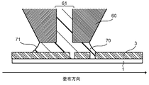
図8は、塗布装置を用いた塗布法により光電変換層22を形成する場合の模式図である。図8には、材料吐出用ヘッド60と、基板1および隔壁部3とを示す。材料吐出用ヘッド60は、例えば塗布装置に設けられる。材料吐出用ヘッド60は、塗布材料が供給されるスリット61を有する。なお、材料吐出用ヘッド60をアプリケータともいう。塗布装置としては、ダイコーター等を用いることができる。このとき、材料吐出用ヘッド60をダイヘッドともいい、スリット61をダイスリットともいう。
FIG. 8 is a schematic view when the
材料吐出用ヘッド60を用いて光電変換層22の材料を塗布する場合、材料吐出用ヘッド60と基板1との間にスリット61を介して光電変換層22の材料を供給し、光電変換層22の材料からなる液溜まり領域70を形成する。液溜まり領域70は、曲面状、いわゆるメニスカス形状の側面71を有する。このとき、光電変換層22の塗布方向における液溜まり領域70の幅は、隔壁部3の延在方向における空隙部320の幅よりも広いことが好ましい。
When applying the material of the
また、隔壁部3の延在方向における空隙部320の周期は1mm以上2mm以下であることが好ましく、光電変換層22の塗布方向における液溜まり領域70の幅は2mm以上4mm以下であることが好ましい。また、上記幅を有する液溜まり領域70に重畳する空隙部320の数を例えば1以上2以下にすることにより、塗布幅のずれを抑制することができる。
The period of the
その後、材料吐出用ヘッド60および基板1の少なくとも一方を塗布方向に沿って移動させながら光電変換層22の材料を塗布して光電変換層22を形成する。
Thereafter, the
次に、図9に示すように、光電変換層22の上面に接し、かつ光電変換層22を挟んで電極21に重畳するように電極23を形成する。
Next, as illustrated in FIG. 9, the
電極23としては、例えば電極21に適用可能な金属または金属酸化物等を用いることができる。基板5を介して光を入射する場合、電極23は透光性を有する。また、電極23が電子輸送層に接する場合、電極23として仕事関数が低い材料を用いることが好ましい。仕事関数の低い材料としては、例えば、アルカリ金属、アルカリ土類金属等が挙げられる。具体的には、Li、In、Al、Ca、Mg、Sm、Tb、Yb、Zr、Na、K、Rb、Cs、Ba、およびこれらの合金を挙げることができる。
As the
電極23は、単層であってもよく、異なる仕事関数の材料で構成される複数の層の積層であってもよい。また、仕事関数が低い材料のうちの1つ以上と、金、銀、白金、銅、マンガン、チタン、コバルト、ニッケル、タングステン、錫などとの合金でもよい。合金の例としては、リチウム−アルミニウム合金、リチウム−マグネシウム合金、リチウム−インジウム合金、マグネシウム−銀合金、マグネシウム−インジウム合金、マグネシウム−アルミニウム合金、インジウム−銀合金、カルシウム−アルミニウム合金等が挙げられる。
The
電極23の厚さは、例えば1nm以上500nm以下、好ましくは10nm以上300nm以下であることが好ましい。1nmよりも薄い場合、電気抵抗が高くなり、発生した電荷が取り出しにくくなる。500nmよりも厚い場合、電極23の成膜に長時間を要するため材料温度が上昇し、光電変換層22にダメージを与え、性能が劣化してしまう。さらに、材料を大量に使用するため、成膜装置を占有する時間が長くなり、コストアップに繋がる。
The thickness of the
電極23は、例えば真空蒸着法、スパッタリング法、イオンプレーティング法、メッキ法、塗布法等で上記導電性を有する材料を成膜することにより形成される。また、光電変換層22に適用可能な塗布法を用いて電極23を形成してもよい。
The
次に、図10に示すように、素子部2を封止し、かつ空隙部320において基板1に接するように、封止部4を形成する。
Next, as shown in FIG. 10, the sealing portion 4 is formed so that the
封止部4としては、例えばガラスフリットや熱硬化性や光硬化性の樹脂等を用いることができる。また、空隙部320に樹脂等を充填しつつ、封止部4を形成することにより、空隙部320において、基板1と封止部4とを固着することができる。封止部4を設けることにより、不純物である酸素や水分と光電変換層22との接触を抑制することができる。
As the sealing part 4, for example, glass frit, thermosetting resin, photocurable resin, or the like can be used. Further, by forming the sealing portion 4 while filling the
空隙部320を設けずに隔壁部3を形成した場合、封止部4が基板1から剥がれやすくなる。これは隔壁部3と封止部4との接着強度が基板1と封止部4との接着強度よりも低いためである。例えば、光電変換装置に応力が与えられた場合、封止部4が隔壁部3を挟んで基板1から剥がれやすくなる。このため、隔壁部3に空隙部320を設けることにより、基板1と封止部4との接着強度を高めることができる。また、同様な理由により、光電変換層を塗布する際の下流側に隔壁部3を延在させないことにより、基板1と封止部4との接着強度をさらに高めることができる。
When the
次に、図11に示すように、素子部2を覆うように封止部4上に基板5を貼り合わせる。このとき、少なくとも第1の電極21と光電変換層22と第2の電極との重畳部が封止されることが好ましい。基板5としては、例えば基板1に適用可能な材料を用いることができる。なお、基板5を介して光を入射させる場合、基板5は透光性を有することが好ましい。
Next, as shown in FIG. 11, a
なお、図12に示すように、素子部2を封止した後、封止部4の外側に位置する光電変換層22の一部および第3の隔壁部33の一部を含むように基板1の一部を切断してもよい。これにより、光電変換装置のサイズを小さくすることができる。
As shown in FIG. 12, after sealing the
以上のように、本実施形態における光電変換装置の製造方法では、少なくとも一端が光電変換領域から周辺領域まで延在する隔壁部を形成することにより、少なくとも光電変換層を塗布する際の助走部を周辺領域に設ける。その後、周辺領域から助走部を含む隔壁部に沿って光電変換層の材料を塗布することにより、塗布幅が制御されるため、光電変換セル同士の間隔を狭くすることができる。 As described above, in the method for manufacturing a photoelectric conversion device according to this embodiment, at least one end of the photoelectric conversion layer is applied by forming a partition wall portion extending from the photoelectric conversion region to the peripheral region. Provided in the peripheral area. Then, since the application | coating width | variety is controlled by apply | coating the material of a photoelectric converting layer along the partition part containing a run-up part from a peripheral region, the space | interval between photoelectric conversion cells can be narrowed.
本実施形態の光電変換装置の製造方法例は、図5ないし図12を参照して説明した製造方法例に限定されない。図13および図14は、光電変換装置の製造方法例を示す平面模式図である。なお、図5ないし図12を参照して説明した製造方法例と共通する部分は、上記説明を適宜援用することができる。 The example of the manufacturing method of the photoelectric conversion device of this embodiment is not limited to the example of the manufacturing method described with reference to FIGS. 13 and 14 are schematic plan views illustrating an example of a method for manufacturing a photoelectric conversion device. The above description can be used as appropriate for portions common to the manufacturing method example described with reference to FIGS.
上記工程と同様に、電極23まで形成した後、図13に示すように第2の隔壁部32の少なくとも一部に沿って光電変換層22の一部を除去し、基板1の一部を露出させることにより、光電変換層22の一部に空隙部220を形成する。例えば、光電変換層22の材料を塗布後に乾燥させて機械的に剥がす、または粘着テープ等で剥がすことにより空隙部220を形成することができる。
Similar to the above process, after forming up to the
その後、図14に示すように、空隙部220において基板1に接するように封止部4を形成する。その後、上記工程と同様に封止部4に基板5を貼り合わせる。上記工程により、基板1と封止部4との接触面積を増やすことができるため、基板1と封止部4との接着強度を高めることができる。
Thereafter, as shown in FIG. 14, the sealing portion 4 is formed so as to be in contact with the
(第2の実施形態)
図15は、横1m×縦1.2mの光電変換パネルの例を示す模式図である。図15に示す光電変換パネルは、1つあたり20〜30cm角の縦4×横3の合計12個の光電変換モジュール100を具備する。光電変換モジュール100は、第1の実施形態の光電変換装置を複数具備する。複数の光電変換モジュールは、互いに直列接続または並列接続で電気的に接続されていてもよい。
(Second Embodiment)
FIG. 15 is a schematic diagram illustrating an example of a photoelectric conversion panel 1 m wide by 1.2 m long. The photoelectric conversion panel shown in FIG. 15 includes a total of twelve
図15に示すように、第1の実施形態における光電変換装置を用いて光電変換モジュールを構成することができ、複数の光電変換モジュールを用いて光電変換パネルを構成することができる。上記光電変換モジュールおよび光電変換パネルは、例えば単位面積あたりの光電変換効率が高いため、例えば自動車や住宅用の太陽電池パネルとしても好適である。 As illustrated in FIG. 15, the photoelectric conversion module can be configured using the photoelectric conversion device according to the first embodiment, and the photoelectric conversion panel can be configured using a plurality of photoelectric conversion modules. Since the photoelectric conversion module and the photoelectric conversion panel have high photoelectric conversion efficiency per unit area, for example, they are also suitable as solar cell panels for automobiles and houses, for example.
実施例として、上記実施形態における第1の隔壁部と、第2の隔壁部と、第3の隔壁部とを有する隔壁部を備える光電変換モジュールと、比較例として隔壁部を備えていない光電変換モジュールと、をそれぞれ作製した。実施例の光電変換モジュールにおいて、隔壁部の材料として、感光性ポリイミドを用い、隔壁部の延在方向に垂直な方向の幅を40μm以上400μm以下とし、隔壁部の延在方向における空隙の幅を1mmとし、隔壁部の厚さを1μmとし、第3の隔壁部の長さを3cmとした。また、金属酸化物からなる電子輸送層と、ポリチオフェン系P型材料とフラーレン誘導体を混合した光活性層と、ポリチオフェン系ポリマー材料からなる正孔輸送層とを順に形成することにより、厚さ0.2μmの光電変換層を形成した。 As an example, a photoelectric conversion module provided with a partition part having the first partition part, the second partition part, and the third partition part in the above embodiment, and a photoelectric conversion without a partition part as a comparative example Each module was produced. In the photoelectric conversion module of the example, photosensitive polyimide is used as the material of the partition wall, the width in the direction perpendicular to the extending direction of the partition wall is set to 40 μm or more and 400 μm or less, and the width of the gap in the extending direction of the partition wall is set. The thickness of the partition wall was 1 μm, and the length of the third partition wall was 3 cm. In addition, an electron transport layer made of a metal oxide, a photoactive layer in which a polythiophene P-type material and a fullerene derivative are mixed, and a hole transport layer made of a polythiophene polymer material are formed in this order, and thereby a thickness of 0. A 2 μm photoelectric conversion layer was formed.
隔壁部を備えていない比較例の光電変換モジュールでは、4mmまでしか光電変換セルの間隔を狭くすることができず、開口率も72%と低かった。これに対し、隔壁部を備える実施例の光電変換モジュールでは、1.2mmまで光電変換セルの間隔を狭くすることができ、開口率を91%まで高くすることができた。このことから、隔壁部を設けることにより、光電変換セルを集積化され、光電変換領域の面積が大きくなり、開口率を高めることができることがわかる。 In the photoelectric conversion module of the comparative example not provided with the partition wall, the interval between the photoelectric conversion cells could be narrowed only up to 4 mm, and the aperture ratio was as low as 72%. On the other hand, in the photoelectric conversion module of an Example provided with a partition part, the space | interval of a photoelectric conversion cell could be narrowed to 1.2 mm, and the aperture ratio could be made to 91%. From this, it can be seen that by providing the partition wall, the photoelectric conversion cells are integrated, the area of the photoelectric conversion region is increased, and the aperture ratio can be increased.
1…基板、1a…第1の領域、1b…第2の領域、1c…第3の領域、2…素子部、21…電極、22…光電変換層、220…空隙部、22a…バッファ層、22b…光活性層、22c…バッファ層、23…電極、3…隔壁部、3a…隔壁部、3b…隔壁部、31…第1の隔壁部、32…第2の隔壁部、320…空隙部、33…第3の隔壁部、4…封止部、5…基板、60…材料吐出用ヘッド、61…スリット、70…液溜まり領域、71…側面、100…光電変換モジュール。
DESCRIPTION OF
Claims (15)
前記第1の領域上に設けられた第1の電極と、前記第1の電極の上面に接するように設けられた光電変換層と、前記光電変換層の上面に接し、かつ前記光電変換層を挟んで前記第1の電極に重畳するように設けられた第2の電極と、を有する素子部と、
前記光電変換層の側面に接するように前記第1の領域上に設けられた第1の隔壁部と、前記第1の隔壁部から前記第2の領域まで延在し、かつ前記第2の領域上に空隙部を含む第2の隔壁部と、を有する隔壁部と、
前記素子部を封止するように設けられ、かつ前記空隙部において前記第2の領域に接する封止部と、を具備する、光電変換装置。 A substrate having a first region and a second region surrounding the first region;
A first electrode provided on the first region, a photoelectric conversion layer provided in contact with an upper surface of the first electrode, an upper surface of the photoelectric conversion layer, and the photoelectric conversion layer A second electrode provided so as to overlap with the first electrode with a sandwich,
A first partition wall provided on the first region so as to be in contact with a side surface of the photoelectric conversion layer; the second partition region extending from the first partition wall portion to the second region; A partition part having a second partition part including a void part on the top,
And a sealing portion provided so as to seal the element portion and in contact with the second region in the gap portion.
前記隔壁部は、前記第2の隔壁部から前記第3の領域まで延在する第3の隔壁部をさらに有する、請求項1に記載の光電変換装置。 The substrate further includes a third region outside the second region,
The photoelectric conversion device according to claim 1, wherein the partition wall further includes a third partition wall extending from the second partition wall to the third region.
前記光電変換層は、前記第3の領域まで延在する、請求項2ないし請求項4のいずれか一項に記載の光電変換装置。 The extending direction of the partition wall is a direction parallel to the application direction of the photoelectric conversion layer,
The photoelectric conversion layer extends to said third region, the photoelectric conversion device according to any one of claims 2 to 4.
複数の前記光電変換セルの間隔は、4.0mm未満である、請求項1ないし請求項7のいずれか一項に記載の光電変換装置。 The element unit includes a plurality of photoelectric conversion cells including the first electrode, the photoelectric conversion layer, and the second electrode,
The photoelectric conversion device according to any one of claims 1 to 7, wherein an interval between the plurality of photoelectric conversion cells is less than 4.0 mm.
前記第1の領域上に設けられた第1の隔壁部と、前記第1の隔壁部から前記第2の領域まで延在し、前記第2の領域に空隙を含む第2の隔壁部と、前記第2の隔壁部から前記第3の領域まで延在する第3の隔壁部と、を有する隔壁部を形成し、
前記第1の隔壁部ないし前記第3の隔壁部に沿って、前記第3の隔壁部から前記第1の隔壁部まで前記基板上に光電変換層の材料を塗布して前記光電変換層を形成し、
前記光電変換層の上面に接し、かつ前記光電変換層を挟んで前記第1の電極に重畳するように第2の電極を形成し、
前記第1の電極と前記光電変換層と前記第2の電極とを有する素子部を封止し、かつ前記空隙において前記基板に接するように封止部を形成する、光電変換装置の製造方法。 Forming a first electrode on the first region of the substrate having a first region, a second region surrounding the first region, and a third region provided outside the second region; And
A first partition provided on the first region; a second partition that extends from the first partition to the second region and includes a gap in the second region; Forming a partition part having a third partition part extending from the second partition part to the third region,
The photoelectric conversion layer is formed by applying a material of a photoelectric conversion layer on the substrate from the third partition wall portion to the first partition wall portion along the first partition wall portion to the third partition wall portion. And
Forming a second electrode in contact with the upper surface of the photoelectric conversion layer and overlapping the first electrode with the photoelectric conversion layer interposed therebetween;
A method for manufacturing a photoelectric conversion device, comprising: sealing an element portion having the first electrode, the photoelectric conversion layer, and the second electrode; and forming a sealing portion so as to be in contact with the substrate in the gap.
前記光電変換層を形成した後に、前記第2の隔壁部の一部に沿って前記光電変換層の一部を除去し、前記基板の一部を露出させることにより、前記光電変換層の一部に第2の空隙を形成し、前記第2の空隙において前記基板に接するように前記封止部を形成する、請求項12または請求項13に記載の光電変換装置の製造方法。 The second partition wall portion includes a first gap composed of the gap,
After forming the photoelectric conversion layer, a part of the photoelectric conversion layer is removed by removing a part of the photoelectric conversion layer along a part of the second partition wall and exposing a part of the substrate. 14. The method for manufacturing a photoelectric conversion device according to claim 12, wherein a second gap is formed in the first gap and the sealing portion is formed so as to be in contact with the substrate in the second gap.
前記液溜まり領域の塗布方向における幅は、前記隔壁部の延在方向における前記空隙の幅よりも広い、請求項12ないし請求項14のいずれか一項に記載の光電変換装置の製造方法。 A material for the photoelectric conversion layer is supplied between the material discharge head of the coating apparatus and the substrate to form a liquid pool region made of the material, and at least one of the material discharge head and the substrate is placed in the coating direction. By forming the photoelectric conversion layer by applying the material while moving along,
The method for manufacturing a photoelectric conversion device according to claim 12, wherein a width of the liquid pool region in the application direction is wider than a width of the gap in an extending direction of the partition wall.
Priority Applications (1)
| Application Number | Priority Date | Filing Date | Title |
|---|---|---|---|
| JP2015053614A JP6034429B2 (en) | 2015-03-17 | 2015-03-17 | Photoelectric conversion device and method for manufacturing photoelectric conversion device |
Applications Claiming Priority (1)
| Application Number | Priority Date | Filing Date | Title |
|---|---|---|---|
| JP2015053614A JP6034429B2 (en) | 2015-03-17 | 2015-03-17 | Photoelectric conversion device and method for manufacturing photoelectric conversion device |
Publications (2)
| Publication Number | Publication Date |
|---|---|
| JP2016174086A JP2016174086A (en) | 2016-09-29 |
| JP6034429B2 true JP6034429B2 (en) | 2016-11-30 |
Family
ID=57009115
Family Applications (1)
| Application Number | Title | Priority Date | Filing Date |
|---|---|---|---|
| JP2015053614A Active JP6034429B2 (en) | 2015-03-17 | 2015-03-17 | Photoelectric conversion device and method for manufacturing photoelectric conversion device |
Country Status (1)
| Country | Link |
|---|---|
| JP (1) | JP6034429B2 (en) |
Families Citing this family (1)
| Publication number | Priority date | Publication date | Assignee | Title |
|---|---|---|---|---|
| JP6600670B2 (en) | 2017-09-15 | 2019-10-30 | 株式会社東芝 | Photoelectric conversion element, manufacturing method thereof, and manufacturing apparatus thereof |
Family Cites Families (4)
| Publication number | Priority date | Publication date | Assignee | Title |
|---|---|---|---|---|
| JP2010062185A (en) * | 2008-09-01 | 2010-03-18 | Mitsubishi Electric Corp | Photoelectric converter and method of manufacturing the same |
| JP2013016668A (en) * | 2011-07-05 | 2013-01-24 | Fujifilm Corp | Manufacturing method of solar cell |
| JP2013016667A (en) * | 2011-07-05 | 2013-01-24 | Fujifilm Corp | Manufacturing method of solar cell |
| JP2014103199A (en) * | 2012-11-19 | 2014-06-05 | Fuji Electric Co Ltd | Organic thin-film solar battery module and manufacturing method thereof |
-
2015
- 2015-03-17 JP JP2015053614A patent/JP6034429B2/en active Active
Also Published As
| Publication number | Publication date |
|---|---|
| JP2016174086A (en) | 2016-09-29 |
Similar Documents
| Publication | Publication Date | Title |
|---|---|---|
| JP5225305B2 (en) | Organic thin film solar cell and method for producing the same | |
| JP5603912B2 (en) | Solar cell module | |
| JP6002264B1 (en) | Solar cell module | |
| JP5323114B2 (en) | Solar cell module | |
| JP5537636B2 (en) | Solar cell and solar cell module | |
| WO2016035432A1 (en) | Photoelectric conversion element, wiring substrate for photoelectric conversion element, method for producing photoelectric conversion element, and photoelectric conversion structure | |
| US10121982B2 (en) | Solar cell, solar cell module, and method for manufacturing solar cell | |
| JP5439418B2 (en) | Organic thin film solar cell module and submodule | |
| JP2011082421A (en) | Method for manufacturing organic photoelectric conversion element, and organic photoelectric conversion element | |
| JP5362017B2 (en) | Organic thin film solar cell | |
| JP6076392B2 (en) | Solar cell module and manufacturing method thereof | |
| JP5051147B2 (en) | Solar cell module and solar power generation device | |
| JP6034429B2 (en) | Photoelectric conversion device and method for manufacturing photoelectric conversion device | |
| US10403838B2 (en) | Photoelectric conversion device | |
| JP6076302B2 (en) | Photoelectric conversion element | |
| JP6010649B2 (en) | Solar cell module and manufacturing method thereof | |
| JP6639267B2 (en) | Photoelectric conversion device | |
| JP5472939B2 (en) | Thin film solar cell module | |
| JP5459681B2 (en) | Organic thin film solar cell | |
| JP2016066645A (en) | Photoelectric conversion element and manufacturing method for photoelectric conversion element | |
| JP2016100357A (en) | Photoelectric conversion device |
Legal Events
| Date | Code | Title | Description |
|---|---|---|---|
| A521 | Request for written amendment filed |
Free format text: JAPANESE INTERMEDIATE CODE: A523 Effective date: 20160711 |
|
| TRDD | Decision of grant or rejection written | ||
| A01 | Written decision to grant a patent or to grant a registration (utility model) |
Free format text: JAPANESE INTERMEDIATE CODE: A01 Effective date: 20160927 |
|
| A61 | First payment of annual fees (during grant procedure) |
Free format text: JAPANESE INTERMEDIATE CODE: A61 Effective date: 20161027 |
|
| R151 | Written notification of patent or utility model registration |
Ref document number: 6034429 Country of ref document: JP Free format text: JAPANESE INTERMEDIATE CODE: R151 |