JP6028894B2 - Image reading apparatus and casing manufacturing method - Google Patents
Image reading apparatus and casing manufacturing method Download PDFInfo
- Publication number
- JP6028894B2 JP6028894B2 JP2012086228A JP2012086228A JP6028894B2 JP 6028894 B2 JP6028894 B2 JP 6028894B2 JP 2012086228 A JP2012086228 A JP 2012086228A JP 2012086228 A JP2012086228 A JP 2012086228A JP 6028894 B2 JP6028894 B2 JP 6028894B2
- Authority
- JP
- Japan
- Prior art keywords
- light guide
- light
- optical element
- imaging optical
- space
- Prior art date
- Legal status (The legal status is an assumption and is not a legal conclusion. Google has not performed a legal analysis and makes no representation as to the accuracy of the status listed.)
- Active
Links
Images


Classifications
-
- H—ELECTRICITY
- H04—ELECTRIC COMMUNICATION TECHNIQUE
- H04N—PICTORIAL COMMUNICATION, e.g. TELEVISION
- H04N1/00—Scanning, transmission or reproduction of documents or the like, e.g. facsimile transmission; Details thereof
- H04N1/00519—Constructional details not otherwise provided for, e.g. housings, covers
- H04N1/00557—Connection or assembly of components or elements
-
- B—PERFORMING OPERATIONS; TRANSPORTING
- B29—WORKING OF PLASTICS; WORKING OF SUBSTANCES IN A PLASTIC STATE IN GENERAL
- B29C—SHAPING OR JOINING OF PLASTICS; SHAPING OF MATERIAL IN A PLASTIC STATE, NOT OTHERWISE PROVIDED FOR; AFTER-TREATMENT OF THE SHAPED PRODUCTS, e.g. REPAIRING
- B29C39/00—Shaping by casting, i.e. introducing the moulding material into a mould or between confining surfaces without significant moulding pressure; Apparatus therefor
- B29C39/02—Shaping by casting, i.e. introducing the moulding material into a mould or between confining surfaces without significant moulding pressure; Apparatus therefor for making articles of definite length, i.e. discrete articles
-
- B—PERFORMING OPERATIONS; TRANSPORTING
- B29—WORKING OF PLASTICS; WORKING OF SUBSTANCES IN A PLASTIC STATE IN GENERAL
- B29C—SHAPING OR JOINING OF PLASTICS; SHAPING OF MATERIAL IN A PLASTIC STATE, NOT OTHERWISE PROVIDED FOR; AFTER-TREATMENT OF THE SHAPED PRODUCTS, e.g. REPAIRING
- B29C45/00—Injection moulding, i.e. forcing the required volume of moulding material through a nozzle into a closed mould; Apparatus therefor
- B29C45/17—Component parts, details or accessories; Auxiliary operations
- B29C45/26—Moulds
- B29C45/2628—Moulds with mould parts forming holes in or through the moulded article, e.g. for bearing cages
-
- H—ELECTRICITY
- H04—ELECTRIC COMMUNICATION TECHNIQUE
- H04N—PICTORIAL COMMUNICATION, e.g. TELEVISION
- H04N1/00—Scanning, transmission or reproduction of documents or the like, e.g. facsimile transmission; Details thereof
- H04N1/024—Details of scanning heads ; Means for illuminating the original
- H04N1/028—Details of scanning heads ; Means for illuminating the original for picture information pick-up
- H04N1/03—Details of scanning heads ; Means for illuminating the original for picture information pick-up with photodetectors arranged in a substantially linear array
- H04N1/031—Details of scanning heads ; Means for illuminating the original for picture information pick-up with photodetectors arranged in a substantially linear array the photodetectors having a one-to-one and optically positive correspondence with the scanned picture elements, e.g. linear contact sensors
- H04N1/0318—Integral pick-up heads, i.e. self-contained heads whose basic elements are a light-source, a lens array and a photodetector array which are supported by a single-piece frame
-
- B—PERFORMING OPERATIONS; TRANSPORTING
- B29—WORKING OF PLASTICS; WORKING OF SUBSTANCES IN A PLASTIC STATE IN GENERAL
- B29L—INDEXING SCHEME ASSOCIATED WITH SUBCLASS B29C, RELATING TO PARTICULAR ARTICLES
- B29L2011/00—Optical elements, e.g. lenses, prisms
- B29L2011/0075—Light guides, optical cables
-
- H—ELECTRICITY
- H04—ELECTRIC COMMUNICATION TECHNIQUE
- H04N—PICTORIAL COMMUNICATION, e.g. TELEVISION
- H04N2201/00—Indexing scheme relating to scanning, transmission or reproduction of documents or the like, and to details thereof
- H04N2201/024—Indexing scheme relating to scanning, transmission or reproduction of documents or the like, and to details thereof deleted
- H04N2201/02487—Manufacturing details
-
- H—ELECTRICITY
- H04—ELECTRIC COMMUNICATION TECHNIQUE
- H04N—PICTORIAL COMMUNICATION, e.g. TELEVISION
- H04N2201/00—Indexing scheme relating to scanning, transmission or reproduction of documents or the like, and to details thereof
- H04N2201/024—Indexing scheme relating to scanning, transmission or reproduction of documents or the like, and to details thereof deleted
- H04N2201/028—Indexing scheme relating to scanning, transmission or reproduction of documents or the like, and to details thereof deleted for picture information pick-up
- H04N2201/03—Indexing scheme relating to scanning, transmission or reproduction of documents or the like, and to details thereof deleted for picture information pick-up deleted
- H04N2201/031—Indexing scheme relating to scanning, transmission or reproduction of documents or the like, and to details thereof deleted for picture information pick-up deleted deleted
- H04N2201/03104—Integral pick-up heads, i.e. self-contained heads whose basic elements are a light source, a lens and a photodetector supported by a single-piece frame
- H04N2201/03108—Components of integral heads
- H04N2201/03125—Light guide upstream of the scanned picture elements
-
- H—ELECTRICITY
- H04—ELECTRIC COMMUNICATION TECHNIQUE
- H04N—PICTORIAL COMMUNICATION, e.g. TELEVISION
- H04N2201/00—Indexing scheme relating to scanning, transmission or reproduction of documents or the like, and to details thereof
- H04N2201/024—Indexing scheme relating to scanning, transmission or reproduction of documents or the like, and to details thereof deleted
- H04N2201/028—Indexing scheme relating to scanning, transmission or reproduction of documents or the like, and to details thereof deleted for picture information pick-up
- H04N2201/03—Indexing scheme relating to scanning, transmission or reproduction of documents or the like, and to details thereof deleted for picture information pick-up deleted
- H04N2201/031—Indexing scheme relating to scanning, transmission or reproduction of documents or the like, and to details thereof deleted for picture information pick-up deleted deleted
- H04N2201/03104—Integral pick-up heads, i.e. self-contained heads whose basic elements are a light source, a lens and a photodetector supported by a single-piece frame
- H04N2201/03108—Components of integral heads
- H04N2201/03141—Photodetector lens
-
- H—ELECTRICITY
- H04—ELECTRIC COMMUNICATION TECHNIQUE
- H04N—PICTORIAL COMMUNICATION, e.g. TELEVISION
- H04N2201/00—Indexing scheme relating to scanning, transmission or reproduction of documents or the like, and to details thereof
- H04N2201/024—Indexing scheme relating to scanning, transmission or reproduction of documents or the like, and to details thereof deleted
- H04N2201/028—Indexing scheme relating to scanning, transmission or reproduction of documents or the like, and to details thereof deleted for picture information pick-up
- H04N2201/03—Indexing scheme relating to scanning, transmission or reproduction of documents or the like, and to details thereof deleted for picture information pick-up deleted
- H04N2201/031—Indexing scheme relating to scanning, transmission or reproduction of documents or the like, and to details thereof deleted for picture information pick-up deleted deleted
- H04N2201/03104—Integral pick-up heads, i.e. self-contained heads whose basic elements are a light source, a lens and a photodetector supported by a single-piece frame
- H04N2201/03108—Components of integral heads
- H04N2201/03145—Photodetector
Description
この発明は、読み取りの対象物からの反射光を結像して正立等倍像を形成する結像光学素子を備える画像読取装置に関するものである。 The present invention relates to an image reading apparatus including an imaging optical element that forms an erecting equal-magnification image by forming an image of reflected light from an object to be read.
従来、イメージスキャナー、ファクシミリ、複写機、金融端末装置等において、コンタクトイメージセンサー(Contact Image Sensor)モジュール(以下、「CISモジュール」と略する)が画像読取装置として用いられている。このCISモジュールは、読み取りの対象物を照明する照明手段と、読み取りの対象物の正立等倍像を結像する結像光学素子と、結像光学素子で結像された正立等倍像を読み取るセンサーとを備え、照明手段により照明された前記対象物からの反射光が結像光学素子により集光されてセンサー上に正立等倍像が形成される。例えば、特許文献1に開示された画像読取装置では、アクリル樹脂などの透明部材から成る棒状の導光体がケース内に収納されて、筐体の上面の左右に設けられた凹部にそれぞれ固定配置され、筐体の導光体の間に設けられた貫通穴にレンズアレイ(結像光学素子)が固定配置されている。
2. Description of the Related Art Conventionally, a contact image sensor module (hereinafter abbreviated as “CIS module”) is used as an image reading device in image scanners, facsimiles, copying machines, financial terminal devices, and the like. The CIS module includes an illuminating unit that illuminates a reading object, an imaging optical element that forms an erecting equal-magnification image of the reading object, and an erecting equal-magnification image formed by the imaging optical element. The reflected light from the object illuminated by the illumination means is condensed by the imaging optical element to form an erecting equal-magnification image on the sensor. For example, in the image reading apparatus disclosed in
ところで、従来、導光体および結像光学素子は、筐体等の保持手段の所定位置に接着剤により固着されているので、画像読取装置を廃棄する場合に、保持手段から導光体および結像光学素子を取り外して分解するのが困難であり、リサイクル性の観点から技術の改善が求められている。 Conventionally, the light guide and the imaging optical element are fixed to a predetermined position of a holding unit such as a housing with an adhesive, and therefore when the image reading apparatus is discarded, the light guide and the connection optical element are disposed from the holding unit. It is difficult to remove and disassemble the image optical element, and improvements in technology are required from the viewpoint of recyclability.
この発明は上記課題に鑑みてなされたものであり、組み立てに接着剤等の固着手段を必要とせず、分解が容易でリサイクル性の向上が図られた画像読取装置を提供し、この画像読取装置が備える筐体の製造方法を提供することを目的とする。 The present invention has been made in view of the above problems, and provides an image reading apparatus that does not require a fixing means such as an adhesive for assembly, is easily disassembled, and is improved in recyclability. It aims at providing the manufacturing method of the housing | casing with which it is equipped.
この発明にかかる画像読取装置は、上記目的を達成するために、光源からの光を読み取り対象物に導光する棒状の導光体を有し前記対象物を照明する照明手段と、前記導光体に並設され、複数のレンズ面が前記導光体の長手方向と同方向に配列された入射面が設けられたレンズアレイを有し前記入射面に入射した前記対象物からの反射光を集光してセンサー上に正立等倍像を形成する結像光学素子と、前記導光体および前記結像光学素子を保持する保持手段と、を備え、前記保持手段によって保持された前記導光体は、前記保持手段によって保持された前記結像光学素子に一部重なって配置され、前記結像光学素子の前記保持手段からの脱離を規制することを特徴とする。
In order to achieve the above object, an image reading apparatus according to the present invention has a rod-shaped light guide that guides light from a light source to an object to be read, illuminating means for illuminating the object, and the light guide A lens array provided with an incident surface arranged in parallel to the body and having a plurality of lens surfaces arranged in the same direction as the longitudinal direction of the light guide, and reflected light from the object incident on the incident surface. comprising forming optical element which forms the erect image is focused on a sensor, and a holding means for holding the light guide and the imaging optical element, the said guide held by the holding means The light body is disposed so as to partially overlap the imaging optical element held by the holding means, and regulates the detachment of the imaging optical element from the holding means .
このように構成された発明では、保持手段によって保持された導光体は、保持手段によって保持された結像光学素子に一部重なって配置されることによって、結像光学素子の保持手段からの脱離を規制するので、導光体および結像光学素子を所定位置に固定配置するのに接着剤等の固着手段を必要とせず、接着剤を用いずに組み立てることにより、廃棄の際に分解が容易でリサイクル性の向上が図られた画像読取装置を提供することができる。
In the invention configured as described above, the light guide held by the holding unit is disposed so as to partially overlap the imaging optical element held by the holding unit. Since desorption is regulated, the light guide and the imaging optical element are fixed at a predetermined position, so that no fixing means such as an adhesive is required, and the assembly is performed without using an adhesive. Therefore, it is possible to provide an image reading apparatus which is easy to improve and can be recycled.
また、前記保持手段は、フレーム部材と、前記フレーム部材の内部空間を第1の空間と第2の空間とに仕切る仕切部材と、を備え、前記導光体および前記結像光学素子は、前記仕切部材の前記第1の空間側に保持され、前記センサーは、前記第2の空間において前記第1の空間側の前記結像光学素子に対向する位置に配置され、前記仕切部材は、前記第1の空間側の前記結像光学素子から出射される光が通過するスリットが形成されているとよい。
Further, the holding means includes a frame member, the first space and the partition member for partitioning into a second space, wherein the light guide and the imaging optical element an internal space of the frame member, the The partition member is held on the first space side, the sensor is disposed at a position facing the imaging optical element on the first space side in the second space, and the partition member is disposed on the first space side . It is preferable that a slit through which light emitted from the imaging optical element on one space side passes is formed .
このように構成すると、フレーム部材の内部空間を第1の空間と第2の空間とに仕切る仕切部材の第1の空間側に導光体および結像光学素子が保持される。そして、センサーは、第2の空間において第1の空間側の結像光学素子に対向する位置に配置され、仕切部材は、第1の空間側の結像光学素子から出射される光が通過するスリットが形成されているので、結像光学素子により、読み取り対象物からの反射光を集光してスリットを介してセンサー上に正立等倍像を形成することができる。また、導光体が保持される第1の空間と、センサーが配置される第2の空間とは、仕切部材により隔離されているので、導光体の光が第2の空間に漏れるおそれが無く、導光体から漏洩した光のセンサーへの入射によるノイズの発生を防止することができる。
If comprised in this way, a light guide and an imaging optical element are hold | maintained at the 1st space side of the partition member which partitions off the internal space of a frame member into 1st space and 2nd space . The sensor is arranged at a position facing the imaging optical element on the first space side in the second space, and the light emitted from the imaging optical element on the first space side passes through the partition member. Since the slit is formed , the imaging optical element can collect the reflected light from the reading object and form an erecting equal-magnification image on the sensor through the slit. Moreover, since the 1st space where a light guide is hold | maintained and the 2nd space where a sensor is arrange | positioned are separated by the partition member, there exists a possibility that the light of a light guide may leak into 2nd space. In addition, it is possible to prevent the occurrence of noise due to the light leaking from the light guide entering the sensor.
また、前記照明手段は、前記光源が実装された光源用基板をさらに有し、前記保持手段は、前記導光体が前記保持手段の長手方向の一端側から挿入される挿入溝をさらに有し、前記挿入溝の一端側から前記導光体が挿入されてその一端側を前記光源用基板で抜け止めするように前記光源用基板の前記光源の実装面を当接させて押さえることにより、前記導光体の前記挿入溝からの脱離を規制して前記導光体を挿入状態に保持するとよい。
The illumination unit further includes a light source substrate on which the light source is mounted, and the holding unit further includes an insertion groove into which the light guide is inserted from one end side in the longitudinal direction of the holding unit. The light guide is inserted from one end side of the insertion groove, and the light source mounting surface of the light source substrate is brought into contact with and pressed down so that the one end side is prevented from being detached by the light source substrate, It is preferable to hold the light guide in an inserted state by regulating the detachment of the light guide from the insertion groove.
このようにすると、挿入溝の一端側から挿入された導光体の一端側が、光源用基板で抜け止めするように光源用基板の光源の実装面を当接させて押さえられているので、導光体の一端側から光源の光を該導光体に確実に入射することができると共に、導光体の挿入溝から長手方向への脱離が光源用基板により規制されて導光体が挿入状態に保持されるので、光源と、導光体の挿入溝からの抜け止めを防止する部材とを個別に設けなくともよいため、装置を構成する部品の簡素化を図ることができる。 In this case, one end side of the light guide inserted from one end side of the insertion groove is pressed against the light source mounting surface of the light source substrate so as to be prevented from coming off by the light source substrate. Light from the light source can be reliably incident on the light guide from one end side of the light body, and the light guide is inserted by being regulated by the light source substrate in the longitudinal direction from the insertion groove of the light guide. Since it is held in the state, it is not necessary to provide the light source and the member for preventing the light guide from coming off from the insertion groove, so that the parts constituting the apparatus can be simplified.
また、前記挿入溝の他端側に、前記導光体を前記挿入溝から脱離する方向に付勢する付勢手段が設けられているとよい。 Moreover, it is good for the other end side of the said insertion groove to provide the urging means which urges | biases the said light guide in the direction which detaches | leaves from the said insertion groove.
このようすれば、導光体の挿入溝への挿入状態において、導光体は付勢手段により挿入溝から長手方向へ脱離する方向に付勢されるので、付勢手段の付勢力により導光体の一端側が光源用基板の光源の実装面に押し付けられて密着し、光源の光を導光体に入射する入射効率の向上を図ることができる。 In this way, when the light guide is inserted into the insertion groove, the light guide is urged by the urging means in the direction of detaching from the insertion groove in the longitudinal direction, so that it is guided by the urging force of the urging means. One end side of the light body is pressed against and closely adheres to the light source mounting surface of the light source substrate, so that it is possible to improve the incident efficiency in which the light from the light source enters the light guide.
また、この発明にかかる筐体の製造方法は、光源からの光を導光体により導光して読み取り対象物に照射し、前記対象物からの反射光を結像光学素子によって集光して形成した正立等倍像をセンサーにより読み取る画像読取装置が備える筐体であって、フレーム部材の内部空間を、前記導光体および前記結像光学素子が配置される第1の空間と前記センサーが配置される第2の空間とに仕切って配設される仕切部材の前記第1の空間側である一方側に、挿入溝と、該挿入溝に並設される凹溝とを形成し、前記挿入溝に前記導光体を挿入し、前記凹溝に前記結像光学素子を嵌挿して、前記導光体および前記結像光学素子を保持する筐体の製造方法において、前記仕切部材の一方側を形成する第1の金型と、前記仕切部材の他方側を形成する第2の金型とを対向配置して成型空間を形成し、前記成型空間に、複数の挿入溝形成用ダイを列状に配置する工程と、前記成型空間に、前記仕切部材の材料となる液体を流し込んで硬化させる工程とを備え、前記第1の金型には、前記挿入溝の底面の一部を形成する第1の底面形成面を有する複数の第1のダイが列状に突設されると共に、前記第1のダイに並設されて、前記凹溝を形成する第2のダイが突設され、各前記挿入溝形成用ダイは、前記挿入溝の底面の残りの一部を形成する第2の底面形成面と、該第2の底面形成面に対向配置されて前記挿入溝に挿入される前記導光体を前記底面に押圧するための押圧面を形成する押圧面形成面とを有し、前記成型空間内において、各前記第1のダイおよび各前記挿入溝形成用ダイが互いに隣り合うように密着配置されることを特徴としている。
The housing manufacturing method according to the present invention guides light from a light source by a light guide and irradiates the object to be read, and condenses the reflected light from the object by an imaging optical element. A housing provided in an image reading device that reads a formed erecting equal-magnification image with a sensor, wherein an inner space of a frame member is formed in a first space in which the light guide and the imaging optical element are arranged, and the sensor Forming an insertion groove and a concave groove juxtaposed to the insertion groove on one side of the first space side of the partition member arranged to be partitioned into a second space where In the method of manufacturing a housing for holding the light guide and the imaging optical element by inserting the light guide into the insertion groove and fitting the imaging optical element into the concave groove, A first mold that forms one side and a second mold that forms the other side of the partition member A mold space is formed by arranging the molds opposite to each other, a plurality of insertion groove forming dies are arranged in a row in the molding space, and a liquid serving as a material for the partition member is poured into the molding space. A plurality of first dies having a first bottom surface forming surface that forms a part of the bottom surface of the insertion groove are projected in a row on the first mold. In addition, a second die is provided in parallel with the first die to form the concave groove, and each of the insertion groove forming dies forms the remaining part of the bottom surface of the insertion groove. A second bottom surface forming surface, and a pressing surface forming surface that forms a pressing surface for pressing the light guide inserted in the insertion groove and pressed against the bottom surface, facing the second bottom surface forming surface. has, in the molding space, each of said first die and each said insertion groove forming die is adjacent It is characterized by being urchin contact arrangement.
このように構成された発明では、フレーム部材の内部空間を、導光体および結像光学素子が配置される第1の空間とセンサーが配置される第2の空間とに仕切って配設される仕切部材の第1の空間側である一方側を形成する第1の金型と、仕切部材の他方側を形成する第2の金型とが対向配置されて成型空間が形成され、該形成空間に複数の挿入溝形成用ダイが列状に配置される。そして、成型空間に、仕切部材の材料となる液体が流し込まれて硬化されることにより画像読取装置の筐体が製造される。 In the invention thus configured, the internal space of the frame member is divided into a first space in which the light guide and the imaging optical element are disposed and a second space in which the sensor is disposed. A molding space is formed by opposingly arranging a first mold that forms one side, which is the first space side of the partition member, and a second mold that forms the other side of the partition member, and the formation space A plurality of insertion groove forming dies are arranged in a row. Then, the casing of the image reading apparatus is manufactured by pouring a liquid as a material for the partition member into the molding space and curing.
第1の金型には、挿入溝の底面の一部を形成する第1の底面形成面を有する複数の第1のダイが列状に突設されると共に、第1のダイに並設されて、凹溝を形成する第2のダイが突設され、各挿入溝形成用ダイは、挿入溝の底面の残りの一部を形成する第2の底面形成面と、該第2の底面形成面に対向配置されて挿入溝に挿入される導光体を底面に押圧するための押圧面を形成する押圧面形成面とを有し、成型空間内において、各第1のダイおよび各挿入溝形成用ダイが互いに隣り合うように密着配置されることにより、挿入溝の底面の形成型が形成されて、仕切部材の一方側に、底面および押圧面を備える挿入溝が形成されると共に、挿入溝に並設された凹溝が形成される。したがって、挿入溝形成用ダイにより挿入溝の押圧面が形成されるが、第2の金型に押圧面を形成する押圧面形成面を有するダイを突設して前記押圧面を形成する場合と異なり、挿入溝形成用ダイが成型物から引抜かれた際に形成される孔が、第2の金型により形成される仕切部材の他方側に連通するおそれがないので、第1の空間と第2の空間とが確実に隔離された状態で、仕切部材の一方側に挿入溝および凹溝が形成された筐体を製造することができる。また、製造された筐体の挿入溝に挿入して配置された導光体の光が、センサーが配置される第2の空間に漏れるおそれがないので、導光体から漏洩した光のセンサーへの入射によるノイズの発生を防止することができる。
また、この発明にかかる画像読取装置は、上記目的を達成するために、光源からの光を読み取り対象物に導光する導光体を有し前記対象物を照明する照明手段と、前記導光体に並設され、入射面に入射した前記対象物からの反射光を集光してセンサー上に正立等倍像を形成する結像光学素子と、前記導光体および前記結像光学素子を保持する保持手段と、を備え、前記結像光学素子は、前記導光体に対向する部分が面取りされた面取り部位を有し、前記保持手段によって保持された前記導光体は、前記保持手段によって保持された前記結像光学素子の前記面取り部位に接するように配置されることで、前記結像光学素子の前記保持手段からの脱離を規制することを特徴とする。
さらに、この発明にかかる画像読取装置は、上記目的を達成するために、光源からの光を読み取り対象物に導光する導光体を有し前記対象物を照明する照明手段と、前記導光体に並設され、入射面に入射した前記対象物からの反射光を集光してセンサー上に正立等倍像を形成する結像光学素子と、前記導光体および前記結像光学素子を保持する保持手段と、を備え、前記導光体は、前記結像光学素子に対向する部分が面取りされた面取り部位を有し、前記保持手段によって保持された前記導光体の前記面取り部位は、前記保持手段によって保持された前記結像光学素子に接するように配置されることで、前記結像光学素子の前記保持手段からの脱離を規制することを特徴とする。
In the first mold, a plurality of first dies having a first bottom surface forming surface that forms a part of the bottom surface of the insertion groove are projected in a row and arranged in parallel with the first die. And a second die for forming a concave groove is provided so that each insertion groove forming die has a second bottom surface forming surface for forming the remaining part of the bottom surface of the insertion groove, and the second bottom surface formation. A pressing surface forming surface that forms a pressing surface for pressing the light guide that is disposed opposite to the surface and inserted into the insertion groove to the bottom surface, and each first die and each insertion groove in the molding space By forming the forming dies so as to be adjacent to each other, a forming mold for the bottom surface of the insertion groove is formed, and an insertion groove having a bottom surface and a pressing surface is formed on one side of the partition member, and the insertion die is inserted. A concave groove arranged in parallel with the groove is formed. Accordingly, the pressing surface of the insertion groove is formed by the insertion groove forming die, and the pressing surface is formed by projecting a die having a pressing surface forming surface that forms the pressing surface on the second mold. In contrast, since the hole formed when the insertion groove forming die is pulled out from the molded product does not communicate with the other side of the partition member formed by the second mold, the first space and the first space The housing in which the insertion groove and the concave groove are formed on one side of the partition member can be manufactured in a state where the two spaces are reliably separated. In addition, since the light of the light guide disposed by being inserted into the insertion groove of the manufactured housing does not leak to the second space in which the sensor is disposed, the light leaked from the light guide to the sensor The generation of noise due to the incident can be prevented.
In order to achieve the above object, an image reading apparatus according to the present invention has a light guide that guides light from a light source to an object to be read and illuminates the object, and the light guide. An imaging optical element that is arranged in parallel with the body and collects reflected light from the object incident on the incident surface to form an erecting equal-magnification image on the sensor, and the light guide and the imaging optical element Holding means for holding, the imaging optical element has a chamfered portion chamfered at a portion facing the light guide, and the light guide held by the holding means holds the holding The detachment of the imaging optical element from the holding means is regulated by being arranged so as to contact the chamfered portion of the imaging optical element held by the means.
Furthermore, in order to achieve the above object, the image reading apparatus according to the present invention includes a light guide that guides light from a light source to a reading object, and illuminates the object, and the light guide. An imaging optical element that is arranged in parallel with the body and collects reflected light from the object incident on the incident surface to form an erecting equal-magnification image on the sensor, and the light guide and the imaging optical element Holding means, and the light guide has a chamfered portion chamfered at a portion facing the imaging optical element, and the chamfered portion of the light guide held by the holding means. Is arranged so as to be in contact with the imaging optical element held by the holding means, thereby restricting detachment of the imaging optical element from the holding means.
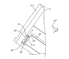
本発明の画像読取装置の一実施形態であるCISモジュールについて図1〜図7を参照して説明する。図1は画像読取装置の一実施形態であるCISモジュールを示す斜視図、図2は図1のA−A線における部分断面斜視図、図3は図1のB−B線における断面斜視図である。図4はCISモジュールが備えるフレームを示す斜視図、図5はCISモジュールが備えるライトガイドを示す斜視図である。図6はCISモジュールの要部拡大図、図7はCISモジュールの裏面図である。 A CIS module which is an embodiment of an image reading apparatus of the present invention will be described with reference to FIGS. 1 is a perspective view showing a CIS module as an embodiment of an image reading apparatus, FIG. 2 is a partial cross-sectional perspective view taken along the line AA in FIG. 1, and FIG. 3 is a cross-sectional perspective view taken along the line BB in FIG. is there. 4 is a perspective view showing a frame provided in the CIS module, and FIG. 5 is a perspective view showing a light guide provided in the CIS module. 6 is an enlarged view of a main part of the CIS module, and FIG. 7 is a back view of the CIS module.
CISモジュール1(本発明の「画像読取装置」に相当)は、原稿ガラスGL上に載置された原稿OBを読み取り対象物として原稿OBに印刷された画像を読み取る装置であり、原稿ガラスGLの直下に配置されている。CISモジュール1は、X方向における原稿OBの読み取り範囲より長く延びる直方体状のフレーム2(本発明の「筐体」「保持手段」に相当)を有しており、フレーム2内に照明手段3、レンズユニット4(本発明の「結像光学素子」に相当)、センサー5、プリント回路基板6がフレーム2に保持されて配置されている。
The CIS module 1 (corresponding to the “image reading device” of the present invention) is a device that reads an image printed on a document OB using a document OB placed on the document glass GL as a reading object. It is arranged directly below. The
フレーム2は、フレーム部材21aおよび中間部材21b(本発明の「仕切部材」に相当)を備え、フレーム部材21aの内部空間は、中間部材21bにより、照明手段3(ライトガイド31)およびレンズユニット4を配置するための上方空間(本発明の「第1の空間」に相当)と、センサー5および照明手段3のLED基板32が設けられたプリント回路基板6を配置するための下方空間(本発明の「第2の空間」に相当)とに区分されて仕切られている。また、中間部材21bの上方空間側には、照明手段3が備えるライトガイド31が挿入されて配置されるための斜溝22と、斜溝22に並設され、レンズユニット4が嵌挿されて配置されるための凹溝23とがX方向に延設されている。凹溝23の底面には、レンズユニット4から出射されて、X方向に所定の読取幅を有する光が通過するためのスリット24がX方向に延設されており、スリット24により、フレーム2の上方空間と下方空間とが連通されている。
The
斜溝22の底面の上方には、斜溝22に配置されたライトガイド31を上方から押圧するための複数の押さえ部材25がX方向において所定の間隔でフレーム2に設けられている。各押さえ部材25は、それぞれ、斜溝22に沿って隣接するフレーム2の側壁(フレーム部材21a)から内側に向けて突出して当該フレーム2と一体的に形成されている。また、押さえ部材25の下面側に配置されるライトガイド31を斜溝22の底面に押圧する押圧面は、押圧対象であるライトガイド31の上側の外周面形状とほぼ同一形状に形成されている。
Above the bottom surface of the
また、斜溝22の一端側(図1の紙面に向かって手前側)から該斜溝22に挿入されたライトガイド31は、平面視において凹溝23に嵌挿されたレンズユニット4にX方向に沿って一部重なって配置される。また、ライトガイド31が押さえ部材25により上方から押圧された状態で、ライトガイド31の出射面31bの下側の長手方向(X方向)に沿って面取りされた部分が、凹溝23に嵌挿された状態のレンズユニット4のケース体41の左上部の長手方向(X方向)に沿って面取りされた部分にX方向に沿って当接する。そして、レンズユニット4は、押さえ部材25によって押圧されるライトガイド31により凹溝23内に向かって押圧されることで、レンズユニット4の凹溝23からのZ矢印の向きと反対方向への脱離が規制されてレンズユニット4が当該凹溝23内に嵌挿状態に保持される。
Further, the
なお、押さえ部材25の押圧面の形状が、押圧対象であるライトガイド31の上側の外周面形状とほぼ同一形状に形成されているので、凹溝23にレンズユニット4が嵌挿され、斜溝22にライトガイド31が挿入された状態において、斜溝22へのライトガイド31の挿入方向(X方向)以外の方向へのライトガイド31の移動、すなわち、斜溝22からの抜けは押さえ部材25により規制されている。また、フレーム2の側壁(フレーム部材21a)の各押さえ部材25に対応する位置には、それぞれ、各押さえ部材の下方を通って斜溝22に連通する矩形状の孔25aが形成されている。この孔25aは、図10〜図13を参照して後で説明するように、フレーム2の上方空間に斜溝22および押さえ部材25を形成するための押さえ部材形成用ダイ203が斜めに配置されることにより形成されたものである。以上のように、斜溝22および押さえ部材25により本発明の「挿入溝」が構成されている。
Since the shape of the pressing surface of the pressing
照明手段3は、プリント回路基板6に取り付けられたLED基板32(本発明の「光源用基板」に相当)に設けられたLED(Light Emitting Diode:図示省略)を光源とし、LEDの光を原稿ガラスGL上に載置された原稿OBに導光するライトガイド31(本発明の「導光体」に相当)を有し原稿OBを照明する。なお、図2中において、LED基板32はその上端部分の形状が点線で示されることにより、その一部が図示省略されている。
The illuminating means 3 uses an LED (Light Emitting Diode: not shown) provided on an LED substrate 32 (corresponding to the “light source substrate” of the present invention) attached to the printed
ライトガイド31は、アクリル樹脂やガラス等の透明部材により形成され、CISモジュール1の読み取り範囲とほぼ同じ長さを有しており、中間部材21bの上面に設けられた斜溝22に挿入されることによりX方向に配設されている。また、ライトガイド31は、一端側の端面(図2の紙面に向かって手前側)からライトガイド31内に入射されたLEDの光を反射する反射構造が形成された反射面31aと、反射面31aにより反射された光を原稿OBに向けて出射する出射面31bとを有している。そして、反射面31aおよび出射面32bは、それぞれライトガイド31の外周面に長手方向に沿って形成されて透明部材を介して対向配置されている。そして、ライトガイド31の長手方向に直交する断面における出射面31bの幅が反射面31aよりも狭く形成されている。
The
また、ライトガイド31の長手方向に直交する断面形状が、反射面31a側から出射面31b側に向けて先細りする六角形状を有し、ライトガイド31は、レンズユニット4に対向する部分が出射面31bに沿って長手方向に面取りされている。そして、ライトガイド31の面取りされた部分が、レンズユニット4の同様に面取りされた部分にX方向に沿って接触配置されることによって、出射面31bがレンズユニット4に近接配置されている。照明手段3は、図5に示すように、ライトガイド31の出射面31bを除く外周面を被覆する遮光フィルム33をさらに有しており、遮光フィルム33のライトガイド31(透明部材)に接する面には光を散乱させる散乱面が形成されている。なお、この実施形態では、遮光フィルム33の厚みは約125μmに形成されている。また、図5では反射面31aに被覆された遮光フィルム33の一部が図示省略されている。
Moreover, the cross-sectional shape orthogonal to the longitudinal direction of the
また、図6および図7に示すように、ライトガイド31を紙面に向かって手前側の一端側から出射面31bをレンズユニット4側に向けてX方向にフレーム2の中間部材21bの上面に形成された斜溝22に挿入することにより、ライトガイド31の手前側の端面の位置に、LED基板32を挿入するための挿入空間SPが形成される。そして、図1および図2に示すように、LED基板32が設けられたプリント回路基板6が、フレーム2の下方空間における所定位置に配設されてLED基板32が挿入空間SPに下方側から挿入されることによって、LED基板32の先端側の端面が押さえ部材25の押圧面に当接することにより位置決めされて、LED基板32に設けられたLEDがライトガイド31の長手方向の一端側である手前側の端面に対向配置される。
Further, as shown in FIGS. 6 and 7, the
LEDからの照明光がライトガイド31の一端側から入射すると、その照明光はライトガイド31の他端側に向けてライトガイド31内を伝播すると共に、反射面31aにより散乱する。反射面31aによって散乱した照明光は、ライトガイド31内において外周面(遮光フィルム33)により全反射されることで出射面31bに向かって集光される。そして、集光された照明光が出射面31bから原稿ガラスGLに向けて出射されて原稿ガラスGL上の原稿OBに集光された状態で照射される。こうして、X方向に延びる帯状の照明光が原稿OBに照射され、原稿OBで反射される。
When illumination light from the LED enters from one end side of the
なお、LEDから照明が入射されるライトガイド31の一端側と反対の他方端側の端面が当接するフレーム2(フレーム部材21a)の内壁面には、スポンジやゴム、ばねなどの弾性部材により形成される付勢手段(図示省略)が設けられている。ライトガイド31は、付勢手段により斜溝22から脱出(脱離)する方向(X矢印の向きと反対方向)に付勢されてLED基板32に設けられたLEDに当接する。挿入空間SPに下方から挿入されたLED基板32は、弾性部材により付勢されたライトガイド31により押圧される方向において、付勢手段が設けられた内壁面に対向するフレーム2の内壁面に当接して位置決めされる。したがって、LED基板32のLEDの実装面に当接するライトガイド31の一端側が、LED基板32により抜け止めするように押さえられることにより、ライトガイド31の斜溝22からの脱離が規制されてライトガイド31の斜溝22への挿入状態が保持されるので、ライトガイド31は、斜溝22内において付勢手段とLED基板32との間に正確に位置決めされて固定される。
In addition, the inner wall surface of the frame 2 (
すなわち、斜溝22の一端側から挿入されたライトガイド31の一端側が、LED基板32で抜け止めするようにLED基板32のLEDの実装面を当接させて押さえられているので、ライトガイド31の一端側からLEDの光をライトガイド31に確実に入射することができると共に、ライトガイド31の斜溝22からの脱離がLED基板32により規制されてライトガイド31が挿入状態に保持されるので、LEDと、ライトガイド31の斜溝22からの抜け止めを防止する部材とを個別に設けなくともよいため、CISモジュール1を構成する部品の簡素化を図ることができる。
That is, one end side of the
また、ライトガイド31の斜溝22への挿入状態において、ライトガイド31は付勢手段により斜溝22から脱離する方向に付勢されるので、付勢手段の付勢力によりライトガイド31の一端側がLED基板32のLEDの実装面に押し付けられて密着するので、LEDの光をライトガイド31に入射する入射効率の向上を図ることができる。
In addition, when the
また、照明手段3が配置されるフレーム2の上方空間と、センサー5(プリント回路基板6)が配置される下方空間とは、中間部材21bにより隔離されているため、照明手段3の光が下方空間に漏れるおそれが無く、照明手段3から漏洩した光のセンサー5への入射によるノイズの発生が防止される。
Further, since the upper space of the
照明手段3による照明光の照射位置の直下位置には、上記した凹溝23がX方向に設けられており、レンズユニット4は、凹溝23に嵌挿されることによりライトガイド31に並設されている。レンズユニット4は、複数のレンズの互いの光軸を平行にして各レンズ面がライトガイド31の長手方向と同じX方向に配列された入射面が設けられたレンズアレイ(図示省略)と、レンズアレイを収納するケース体41とを有し、入射面に入射した原稿OBからの反射光を集光してセンサー5上に原稿OBの正立等倍像を形成する。
The
レンズアレイは、CSIモジュール1の読み取り範囲とほぼ同じ長さだけX方向に延設されており、照明光に対して光透過性を有する樹脂やガラスなどの透明媒体によって一体成形されている。また、レンズアレイの入射側のケース体41には各レンズそれぞれに対応する位置に穿設された複数の貫通孔(図示省略)がX方向に沿って形成されており、原稿OBから入射される反射光の入射方向が各貫通孔により規制される。また、レンズアレイの出射側のケース体41には各レンズそれぞれに対応する位置に穿設された複数の貫通孔(図示省略)がX方向に沿って形成されており、レンズアレイから出射する出射光の出射方向が各貫通孔により規制される。
The lens array extends in the X direction by substantially the same length as the reading range of the
すなわち、レンズアレイの入射側および出射側において、それぞれ複数の貫通孔がX方向に沿って形成されたケース体41は、レンズアレイに対するアパーチャー部材として機能しており、センサー5への迷光の入射すが防止されている。なお、フレーム2の中間部材21bに設けられた凹溝23の底面にX方向に形成されたスリット24は、レンズアレイを構成する各レンズの出射側の各光軸がX方向に配列される位置に形成され、スリット24は、各レンズの出射側の各光軸のX方向における幅よりも多少幅広に形成されている。そして、レンズユニット4に入射した反射光は、スリット24を通過して該スリット24に対向する位置に配置されたセンサー5上に集光されて、該センサー5上に正立等倍像が形成される。
That is, the
ケース体41は、ライトガイド31に対向する部分がX方向に沿って面取りされており、上記したように、当該面取り部分にライトガイド31の面取りされた部分が当接して凹溝23内に向かってケース体41を押圧することにより、レンズユニット4(ケース体41)はフレーム2の凹溝23内に固定される。
The portion of the
センサー5は、図2に示すように、LED基板32が搭載されたプリント回路基板6にX方向に取り付けられており、原稿OBの正立等倍像を読み取り、その正立等倍像に関連する信号を出力する。
As shown in FIG. 2, the
以上のように構成されたCISモジュール1は次のようにして組立てられる。すなわち、図6および図7に示すように、まず、フレーム2の上方空間側に設けられた凹溝23にレンズユニット4が嵌挿されて、ライトガイド31が、斜溝22内に挿入される。そして、図1および図2に示すように、挿入空間SPにLED基板32が下方側から挿入されるように、フレーム2の下方空間の所定位置にプリント回路基板6が配置されることによってCISモジュール1の組み立てが完了する。
The
次に、図8(a),(b)を参照してライトガイド31とレンズユニット4との配置関係の一例について説明する。図8はライトガイドによる原稿の照明状態を説明するための図であって、(a)はライトガイドおよびレンズユニットの配置関係を示し、(b)は原稿の照明状態を示す。また、図8(b)において、Y方向における原点Oの位置はX方向に直交する断面におけるレンズユニット4の光軸CLの位置に相当し、Y(+)方向はレンズユニット側を示し、Y(−)方向はライトガイド側を示し、原点O側がLEDにより照明光が入射されたライトガイド31の端面側を示す。また、図8(b)は、サイバネットシステム株式会社製の照明解析ソフト「LightTools」によるシミュレーションにより導出された光軸CLの位置のX方向における明るさを表している。
Next, an example of the arrangement relationship between the
この実施形態では、ライトガイド31の長手方向に直交する断面における反射面31aの幅が2mm、出射面31bの幅が0.8mm、反射面31aと出射面31bとの距離が4mmに設定されている。また、原稿ガラスGLは屈折率nが1.51の材質により形成されているので、ライトガイド31の出射面31bの法線と原稿ガラスGLとが成す角度がγであれば、原稿ガラスGLに入射して屈折した光の進行方向と原稿ガラスGLとが成す角度δはsinδ=(sinγ)/1.51となる。
In this embodiment, the width of the reflecting
したがって、レンズユニット4の上端面と原稿ガラスGLの下面との距離をd1、原稿ガラスGLの厚みをdとすると、ライトガイド31から出射された光が原稿ガラスGLの上面とレンズユニット4の光軸CLとの交点に照射されるためには、ライトガイド31の長手方向に直交する断面における出射面31bの中心とレンズユニット4の光軸CLとの距離Lは、
L=d1/tan(γ)+d/tan(δ)
と表すことができる。この実施形態では、レンズユニット4の上端面と原稿ガラスGLの下面との距離d1が0.66mm、原稿ガラスGLの厚みdが2.8mmに設定されているため、例えば、ライトガイド31の出射面31bの法線と原稿ガラスGLとが成す角度γを40度とすれば、出射面31bの中心とレンズユニット4の光軸CLとの距離Lは約2.4mmとなる。したがって、上記した条件において、出射面31bの中心および光軸CL間の距離が2.4mmとなるように、ライトガイド31およびレンズユニット4が配置されれば、出射面31bから出射される照明光により、原稿OBの光軸CLの位置が適正にX方向に帯状に照明される。
Therefore, if the distance between the upper end surface of the
L = d1 / tan (γ) + d / tan (δ)
It can be expressed as. In this embodiment, the distance d1 between the upper end surface of the
また、図8(a)に示すように、フレーム2の側壁および押さえ部材25の上面とレンズユニット4のケース体41の貫通孔が形成された上端面とがはほぼ同一の平面Sに配置されるように構成されており、ライトガイド31は平面Sを越えて原稿ガラスGLに突出しないように配置されている。
Further, as shown in FIG. 8A, the side wall of the
なお、この実施形態では、ライトガイド31には、出射面31bとの角度αが100度〜140度となるように面取りが施されており、レンズユニット4には、上端面との角度βが100度〜140度となるように面取りが施されている。したがって、距離Lが2.4mm以内となるようにライトガイド31およびレンズユニット4の入射面が近接配置されると共に、上記したライトガイド31の面取り角度α、レンズユニット4の面取り角度β、光線の入射角度γの関係が、
α+β+γ=270度
となるように、ライトガイド31およびレンズユニット4が配置されることによって、ライトガイド31の出射面31bから出射された光が原稿ガラスGLの上面とレンズユニット4の光軸CLとが交わる部分に帯状に照射される。
In this embodiment, the
By arranging the
すなわち、図8(b)に示すように、照射中心が微小にライトガイド31側に寄った状態で、原稿ガラスGLの上面とレンズユニット4の光軸CLとが交わる部分に対してライトガイド31の出射面31bから出射された光が帯状に19.2%の光利用効率で適正に照射される。
That is, as shown in FIG. 8B, the
(比較例)
次に、図9(a),(b)を参照して比較例について説明する。図9は比較例における原稿の照明状態を説明するための図であって、(a)はライトガイドおよびレンズユニットの配置関係を示し、(b)は原稿の照明状態を示す。図9(a)に示すように、比較例では、ライトガイド131およびレンズユニット104は、それぞれ外周面に上記したような面取りが施されておらず、それぞれ長手方向(X方向)に直交する断面形状が矩形状に形成されている。また、長手方向に直交する断面におけるライトガイド131の出射面31bの幅は反射面31aと同じ幅に形成されている。その他の構成は上記した例と同様であるため、同一符号を付すことによりその説明を省略する。
(Comparative example)
Next, a comparative example will be described with reference to FIGS. 9 (a) and 9 (b). FIGS. 9A and 9B are diagrams for explaining the illumination state of the document in the comparative example. FIG. 9A shows the arrangement relationship between the light guide and the lens unit, and FIG. 9B shows the illumination state of the document. As shown in FIG. 9A, in the comparative example, the
この比較例では、ライトガイド131およびレンズユニット104それぞれに面取りが施されておらず、ライトガイド131およびレンズユニット104を近接配置するとができない。さらに、ライトガイド131に入射されたLEDの照明光は出射面31bに向かって集光されない。したがって、図9(b)に示すように、照射中心が大幅にライトガイド131側に寄った状態となり、原稿ガラスGLの上面とレンズユニット4の光軸CLとが交わる部分がライトガイド131の出射面31bから出射された光によりほぼ照明されない状態となる。
In this comparative example, the
また、図9(b)に点線で示すように、原稿ガラスGLの上面とレンズユニット4の光軸CLとが交わる部分がライトガイド131の出射面31bから出射された光により照明されるためには、ライトガイド131を平面Sを大幅に越えて上方に配置しなければならないが、原稿ガラスGLがCISモジュール1の直上に配置されるため、事実上、同図(b)中の点線の位置にライトガイド131を配置するのは不可能である。
Further, as shown by a dotted line in FIG. 9B, the portion where the upper surface of the original glass GL and the optical axis CL of the
(フレームの成型方法)
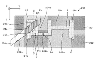
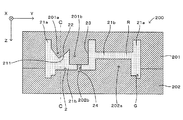
次に、図2および図3を参照しつつ図10〜図13を参照してフレームの成型方法(製造方法)の一例について説明する。図10はフレームを成型するための金型を示す斜視図、図11は図2に示すフレームの断面に相当する位置における金型の断面図、図12は図3に示すフレームの断面に相当する位置における金型の断面図である。また、図13は金型と押さえ部材形成用ダイとの配置関係を説明するための模式図であって、図11および図12のC−C線におけるX−Z平面に平行な断面図である。フレーム2を成型するための金型200は、中間部材21bの一方側を形成する上部金型201(本発明の「第1の金型」に相当)と、中間部材21bの他方側を形成する下部金型202(本発明の「第2の金型」に相当)と、斜溝22の底面および押さえ部材25の押圧面を形成する押さえ部材形成用ダイ203(本発明の「挿入溝形成用ダイ」に相当)とを備えている。
(Frame molding method)
Next, an example of a frame molding method (manufacturing method) will be described with reference to FIGS. 10 to 13 with reference to FIGS. 10 is a perspective view showing a mold for molding the frame, FIG. 11 is a sectional view of the mold at a position corresponding to the cross section of the frame shown in FIG. 2, and FIG. 12 is equivalent to a cross section of the frame shown in FIG. It is sectional drawing of the metal mold | die in a position. FIG. 13 is a schematic view for explaining the positional relationship between the mold and the pressing member forming die, and is a cross-sectional view parallel to the XZ plane along line CC in FIGS. 11 and 12. . The
また、上部金型201の下面側には、第1の空間側に配置される中間部材21bの一方側(上面)に斜溝22の底面の一部を形成するための第1の底面形成面211を有する複数の第1のダイ201aがX方向に列状に突設されると共に、ダイ201aに並設されて、凹溝23を形成するための第2のダイ201bが突設されている。また、下部金型202の上面側には、第2の空間側に配置される中間部材21bの他方側(下面)の形状を形成するためのダイ202aおよびスリット24を形成するためのダイ202bが突設されている。また、下部金型202には、紙面に向かって左側の側面から上面に連通する複数の斜孔202cが長手方向(X方向)に沿って設けられており、各斜孔202cには、側面側から上面側にその先端が突出するように押さえ部材形成用ダイ203が挿入される。
Further, on the lower surface side of the
押さえ部材形成用ダイ203は、第1の空間側に配置される中間部材21bの一方側(上面)に斜溝22の底面の残りの一部を形成するための第2の底面形成面213と、底面形成面211に対向配置されて斜溝22に挿入されるライトガイド31を斜溝22の底面に押圧するための押さえ部材25の押圧面を形成するための押圧面形成面223とを有している。なお、下部金型202の上面から突出する各押さえ部材形成用ダイ203の先端の上面側の押圧面形成面223の形状は、フレーム2の斜溝22に挿入されるライトガイド31の上側の周側面の形状とほぼ同一の形状に形成されている。
The pressing
そして、各押さえ部材形成用ダイ203が下部金型202の各斜孔202cに挿入された状態で、下部金型202の上面に上部金型201の下面を密着して上部金型201および下部金型202が係合されることにより、上部金型201の下面と下部金型202の上面と間に、フレーム2を形成するための樹脂等の液体Rが充填される成型空間Gが形成される。なお、図13に示すように、上部金型201の下面に設けられた斜溝22を形成するためのダイ201aは、上部金型201および下部金型202が組み合わされた状態で、成型空間G内において、下部金型202の上面側に突出する各押さえ部材形成用ダイ203の間に隙間なくはまり込むように形成されている。すなわち、上部金型201のダイ201aおよび押さえ部材形成用ダイ203が長手方向(X方向)に密着して交互に配列されることによって、密着配置されたダイ201aおよび押さえ部材形成用ダイ203の下側の底面形成面211,213によりフレーム2の斜溝22の底面を形成するための型が形成され、押さえ部材形成用ダイ203の上側の押圧面形成面223により押さえ部材25の押圧面を形成するための型が形成される。
Then, in a state where each pressing
このように構成された上部金型201、下部金型202および押さえ形成用ダイ203が組み合わされることによって、上部金型201と下部金型202とが対向配置されて成型空間Gが形成され、成型空間に複数の押さえ部材形成用ダイ203が配置される。そして、成型空間Gに溶融された樹脂等の液体Rが流し込まれ、液体Rが加熱や紫外線照射されることにより硬化されて、押さえ部材形成用ダイ203が抜き取られた後に、上部金型201および下部金型202が取り外されることによりフレーム2が完成する。
By combining the
以上のように、上記した実施形態では、斜溝22に挿入されたライトガイド31が、平面視において、斜溝22に並設された凹溝23に嵌挿されたレンズユニット4に一部重なって配置されることによって、ライトガイド31により、レンズユニット4の凹溝23からの脱離が規制されてレンズユニット4が嵌挿状態に保持されているので、ライトガイド31およびレンズユニット4をフレーム2の所定位置に固定配置するのに接着剤等の固着手段を必要とせず、接着剤を用いずにCISモジュール1を組み立てることにより、廃棄の際に分解が容易でリサイクル性の向上が図られたCISモジュール1を提供することができる。
As described above, in the above-described embodiment, the
また、押さえ部材形成用ダイ203により押さえ部材25の押圧面が形成されるが、下部金型202に押圧面を形成する押圧面形成面を有するダイを突設して該押圧面を形成する場合と異なり、押さえ部材形成用ダイ203が成型物(フレーム2)から引抜かれた際に形成される孔が、下部金型202により形成される中間部材21bの他方側(下方空間)に連通するおそれがない。
The pressing surface of the pressing
すなわち、押さえ部材形成用ダイ203が、中間部材21bに相当する位置よりも上方において、上部金型201および下部金型202が組み合わされた金型200内に側方から挿入されることによって、フレーム2の斜溝22の上方に配置される押さえ部材25が形成されるので、フレーム2が形成される際に、正立等倍像をセンサー5上に形成するためにレンズユニット4から出射される光が通過するためのスリット24の他に、上方空間と下方空間とを連通する孔(穴)が中間部材21bに形成されるおそれが無い。そのため、上方空間と下方空間とが確実に隔離された状態で、中間部材21bの一方側の上面に斜溝22(押さえ部材25)および凹溝23が形成されたフレーム2を成型することができる。したがって、成型されたフレーム2の斜溝22に挿入されて上方空間に配置されたライトガイド31の光が、センサー5が配置される下方空間に漏れるおそれが無いので、ライトガイド31から漏洩した光のセンサー5への入射によるノイズの発生を確実に防止することができる。また、照明手段3の光がセンサー5に漏洩するのを確実に防止することができるので、ライトガイド31を被覆する遮光フィルム33を省略することもできる。
That is, the pressing
また、LEDの光を原稿OBに導光する棒状のライトガイド31は、透明部材により形成されている。また、ライトガイド31は、該ライトガイド31の少なくとも一方の端面から当該ライトガイド31内に入射されたLEDの光を反射する反射構造が形成された反射面31aと、反射面31aにより反射された光を原稿OBに向けて出射する出射面31bとを有しており、反射面31aおよび出射面31bは、それぞれ当該ライトガイド31の外周面に長手方向(X方向)に沿って形成されて透明部材を介して対向配置されている。そして、ライトガイド31の長手方向に直交する断面における出射面31bの幅が反射面31aよりも狭く形成されているので、ライトガイド31の端面から入射されて反射面31aにおいてその長手方向全体に渡って散乱したLEDの光が、透明部材の内部においてライトガイド31の外周面により全反射されて出射面31bに向かって集光されて該出射面31bから原稿OBに向けて帯状に出射される。
Further, the rod-shaped
したがって、ライトガイド31の内部において出射面31bに向かって集光された状態の光が該出射面31bから原稿OBに向かって帯状に出射されるので、原稿OBとレンズユニット4が備えるレンズアレイの光軸CLとが交わる部分を照明手段3により帯状に効率よく照明することが可能な照明手段3を備えるCISモジュール1を提供することができる。
Accordingly, light in a state of being condensed toward the
また、ライトガイド31の長手方向に直交する断面形状が反射面31a側から出射面31b側に向けて先細りする形状であるので、反射面31aにおいてその長手方向全体に渡って散乱したLEDの光を、ライトガイド31の外周面によって全反射させることによりさらに効率よく出射面31bに向かって集光することができる。したがって、出射面31bから原稿OBに向けて帯状に出射される光によって原稿OBをさらに効率よく照明することができる。また、ライトガイド31の長手方向に直交する断面形状が反射面31a側から出射面31b側に向けて先細りする形状であるため、長手方向(X方向)に直交する断面における出射面31bの中心と、各レンズ面の配列方向(X方向)に直交する断面におけるレンズアレイの光軸CLとをより近接して配置することができる。
Further, since the cross-sectional shape perpendicular to the longitudinal direction of the
また、ライトガイド31は、レンズユニット4に対向する部分が出射面31bに沿って長手方向に面取りされているので、長手方向に直交する断面における出射面31bの中心と、各レンズ面の配列方向に直交する断面におけるレンズユニット4の光軸CLとをより近接配置して、該光軸CL上のレンズユニットの4の複数の貫通孔が形成された上端面により近い位置を照明手段3により帯状に照明することができる。また、ライトガイド31の出射面31bとレンズユニット4の入射面とが近接配置されることによってCISモジュールの小型化を図ることができる。
In addition, since the
また、レンズアレイを収納するケース体41のライトガイド31に対向する部分がレンズ面の配列方向に沿って面取りされているので、ライトガイド31の長手方向に直交する断面における出射面31bの中心と、各レンズ面の配列方向に直交する断面におけるレンズユニット4の光軸CLとをさらに近接配置することができる。
In addition, since the portion of the
また、ライトガイド31を形成する透明部材内において反射面31aにより反射された光を、遮光フィルム33の散乱面によってより効率よく全反射させることでさらに効率よく出射面31bに向かって集光することができる。また、遮光フィルム33により、ライトガイド31に入射されたLEDの光がライトガイド31の外周面から外部に漏れるのを防止することができる。また、従来では、光の漏洩を防止するためにライトガイド31はケースに収納されてフレーム2に設けられていたが、上記したようにライトガイド31を、ケースと比較すると非常に薄い遮光フィルム33で被覆することによって光の漏洩を防止することで、ライトガイド31およびレンズユニット4をより近接して配置することができる。
Further, the light reflected by the reflecting
なお、本発明は上記した実施形態に限定されるものではなく、その趣旨を逸脱しない限りにおいて上述したものに対して種々の変更を加えることが可能である。例えば、ライトガイド31またはレンズユニット4に施される面取りの態様は上記した例に限るものではなく、斜溝22に挿入されたライトガイド31により、凹溝23に嵌挿されたレンズユニット4を確実に押圧することができれば、ライトガイド31またはレンズユニット4にどのように面取りが施されていてもよい。また、ライトガイド31によりレンズユニット4を凹溝23に押圧することができれば、ライトガイド31またはレンズユニット4に必ずしも面取りが施されている必要はないが、ライトガイド31およびレンズユニット4を近接配置して、ライトガイド31の出射面31bから出射された光がレンズユニット4の光軸CL上に適切に照射されるように、ライトガイド31またはレンズユニット4に面取りを施すのが好ましい。
The present invention is not limited to the above-described embodiments, and various modifications can be made to the above-described ones without departing from the gist thereof. For example, the chamfering mode applied to the
また、レンズユニット4(結像光学素子)の構成は、センサー5上に適正に正立等倍像を形成することができるものであればどのようなものであってもよく、1列のレンズ列により構成されたレンズアレイや複数のレンズ列が配列された構成のレンズアレイなどを採用することができる。また、レンズアレイの入射側および出射側にそれぞれアパーチャー部材が配置された結像光学素子や、複数のレンズアレイが光軸方向に配列され、入射側、レンズアレイ間、出射側にそれぞれアパーチャー部材が配置されて構成された結像光学素子などを採用することができる。また、SLA(セルフォック(登録商標)レンズアレイ)により結像光学素子が構成されていてもよい。
The lens unit 4 (imaging optical element) may have any configuration as long as it can properly form an erecting equal-magnification image on the
また、上記した実施形態では、押さえ部材形成用ダイ203を利用してフレーム2に押さえ部材25を一体的に成型したが、押さえ部材形成用ダイ203の換わりに、下部金型202の上面に、押さえ部材25の押圧面と同一の先端面形状を有するダイを突設することにより、フレーム2に押さえ部材25を形成してもよい。
Further, in the above-described embodiment, the pressing
また、ライトガイド31の長手方向に直交する断面形状は、上記した六角形状に限らず、台形や長方形、五角形状など、どのような形状であってもよい。
Moreover, the cross-sectional shape orthogonal to the longitudinal direction of the
そして、読み取りの対象物からの反射光を結像して正立等倍像を形成する結像光学素子を備える画像読取装置に本発明を広く適用することができる。 The present invention can be widely applied to an image reading apparatus including an imaging optical element that forms an erecting equal-magnification image by forming an image of reflected light from an object to be read.
1…CISモジュール(画像読取装置)、 2…フレーム(筐体、保持手段)、 21a…フレーム部材、 21b…中間部材(仕切部材)、 22…斜溝(挿入溝)、 23…凹溝、 24…スリット、 25…押さえ部材(挿入溝)、 3…照明手段、 31…ライトガイド(導光体)、 32…LED基板(光源用基板)、 4…レンズユニット(結像光学素子)、 5…センサー、 201…上部金型(第1の金型)、 201a…第1のダイ、 201b…第2のダイ、 211…第1の底面形成面、 202…下部金型(第2の金型)、 203…押さえ部材形成用ダイ(挿入溝形成用ダイ)、 213…第2の底面形成面、 223…押圧面形成面、 G…成型空間、 R…液体
DESCRIPTION OF
Claims (6)
前記導光体に並設され、複数のレンズ面が前記導光体の長手方向と同方向に配列された入射面が設けられたレンズアレイを有し前記入射面に入射した前記対象物からの反射光を集光してセンサー上に正立等倍像を形成する結像光学素子と、
前記導光体および前記結像光学素子を保持する保持手段と、
を備え、
前記保持手段は、
前記導光体が挿入される挿入溝と、
前記長手方向と交差する一端面に形成され、前記挿入溝に連通して前記導光体を前記挿入溝に挿入する挿入口と、
前記挿入溝に並設され、前記レンズアレイに対して反射光が入射する入射方向側から当該結像光学素子が嵌挿される凹溝と、を備え、
前記凹溝に嵌挿された前記結像光学素子に対して、前記挿入口から前記挿入溝に挿入された前記導光体が、前記入射方向側からの平面視において一部重なって配置されることによって、前記結像光学素子の前記保持手段からの脱離を規制する、
ことを特徴とする画像読取装置。 An illumination means for illuminating the object having a rod-shaped light guide that reads light from the light source and guides the light to the object;
The lens array is provided in parallel with the light guide, and a plurality of lens surfaces are arranged in the same direction as the longitudinal direction of the light guide. An imaging optical element that collects the reflected light to form an erecting equal-magnification image on the sensor; and
Holding means for holding the light guide and the imaging optical element;
With
The holding means is
An insertion groove into which the light guide is inserted;
An insertion port that is formed on one end surface intersecting the longitudinal direction and communicates with the insertion groove to insert the light guide into the insertion groove;
A concave groove arranged in parallel with the insertion groove and into which the imaging optical element is inserted from the incident direction side where the reflected light is incident on the lens array;
The light guide inserted into the insertion groove from the insertion port is partially overlapped with the imaging optical element inserted into the concave groove in plan view from the incident direction side. it allows regulating the detachment from the holding means of the imaging optical element,
An image reading apparatus.
フレーム部材と、
前記フレーム部材の内部空間を第1の空間と第2の空間とに仕切る仕切部材と、を備え、
前記導光体および前記結像光学素子は、前記仕切部材の前記第1の空間側に保持され、
前記センサーは、前記第2の空間において前記第1の空間側の前記結像光学素子に対向する位置に配置され、
前記仕切部材は、前記第1の空間側の前記結像光学素子から出射される光が通過するスリットが形成されている請求項1に記載の画像読取装置。 The holding means is
A frame member;
A partition member that partitions the internal space of the frame member into a first space and a second space;
The light guide and the imaging optical element are held on the first space side of the partition member,
The sensor is disposed at a position facing the imaging optical element on the first space side in the second space,
The image reading apparatus according to claim 1, wherein the partition member is formed with a slit through which light emitted from the imaging optical element on the first space side passes.
前記挿入溝の一端側の前記挿入口から前記導光体を前記光源用基板で抜け止めするように前記光源用基板の前記光源の実装面を当接させて押さえることにより、前記導光体の前記挿入溝からの脱離を規制して前記導光体を挿入状態に保持する請求項1または2に記載の画像読取装置。 The illumination means further includes a light source substrate on which the light source is mounted ,
By pressing by contacting the mounting surface of the light source of the light source substrate to retaining the light guide at substrate the light source from the insertion opening on one end side of the insertion groove, of the light guide The image reading apparatus according to claim 1, wherein the light guide is held in an inserted state by restricting detachment from the insertion groove.
前記仕切部材の一方側を形成する第1の金型と、前記仕切部材の他方側を形成する第2の金型とを対向配置して成型空間を形成し、前記成型空間に、複数の挿入溝形成用ダイを列状に配置する工程と、
前記成型空間に、前記仕切部材の材料となる液体を流し込んで硬化させる工程とを備え、
前記第1の金型には、前記挿入溝の底面の一部を形成する第1の底面形成面を有する複数の第1のダイが列状に突設されると共に、前記第1のダイに並設されて、前記凹溝を形成する第2のダイが突設され、
各前記挿入溝形成用ダイは、前記挿入溝の底面の残りの一部を形成する第2の底面形成面と、該第2の底面形成面に対向配置されて前記挿入溝に挿入される前記導光体を前記底面に押圧するための押圧面を形成する押圧面形成面とを有し、
前記成型空間内において、各前記第1のダイおよび各前記挿入溝形成用ダイが互いに隣り合うように密着配置される、
ことを特徴とする筐体の製造方法。 Image reading in which light from a light source is guided by a light guide to irradiate an object to be read, and an erecting equal-magnification image formed by condensing reflected light from the object by an imaging optical element is read by a sensor A housing provided in the apparatus, wherein an internal space of the frame member is partitioned into a first space in which the light guide and the imaging optical element are disposed and a second space in which the sensor is disposed. An insertion groove and a concave groove arranged in parallel with the insertion groove are formed on one side which is the first space side of the partition member provided, and the light guide is inserted into the insertion groove, In the manufacturing method of the housing for fitting the imaging optical element into the concave groove and holding the light guide and the imaging optical element,
A molding space is formed by disposing a first mold that forms one side of the partition member and a second mold that forms the other side of the partition member, and a plurality of inserts are inserted into the molding space. Arranging the grooves forming dies in a row;
A step of pouring and hardening a liquid as a material of the partition member into the molding space;
A plurality of first dies having a first bottom surface forming surface forming a part of a bottom surface of the insertion groove are provided in the first die so as to protrude in a row, and the first die is provided with the first die. A second die that is juxtaposed to form the concave groove is projected,
Each of the insertion groove forming dies has a second bottom surface forming surface that forms the remaining part of the bottom surface of the insertion groove, and is disposed opposite to the second bottom surface forming surface to be inserted into the insertion groove. A pressing surface forming surface that forms a pressing surface for pressing the light guide against the bottom surface;
In the molding space, the first dies and the insertion groove forming dies are arranged in close contact with each other,
A method for manufacturing a casing, characterized by that.
前記導光体は、前記結像光学素子に対向する部分が前記出射面に沿って前記長手方向に面取りされた面取り部位を有し、
前記保持手段によって保持された前記導光体の前記面取り部位と、前記保持手段によって保持された前記結像光学素子の前記面取り部位とが接するとともに、前記出射面が前記結像光学素子の前記入射面を延長した面から突出しないように配置される、ことで、前記結像光学素子の前記保持手段からの脱離を規制する、
ことを特徴とする請求項1から4に記載の画像読取装置。 The imaging optical element has a chamfered portion in which a portion facing the light guide is chamfered along the arrangement direction of the lens surfaces ;
The light guide has a chamfered portion where a portion facing the imaging optical element is chamfered in the longitudinal direction along the emission surface;
The chamfered portion of the light guide held by the holding means is in contact with the chamfered portion of the imaging optical element held by the holding means, and the exit surface is the incident of the imaging optical element. It is arranged so that it does not protrude from the extended surface, thereby restricting detachment of the imaging optical element from the holding means,
The image reading apparatus according to claim 1, wherein:
Priority Applications (4)
| Application Number | Priority Date | Filing Date | Title |
|---|---|---|---|
| JP2012086228A JP6028894B2 (en) | 2012-04-05 | 2012-04-05 | Image reading apparatus and casing manufacturing method |
| TW102110751A TWI526043B (en) | 2012-04-05 | 2013-03-26 | Image reading device and method of manufacturing housing |
| US13/852,245 US9083832B2 (en) | 2012-04-05 | 2013-03-28 | Image reading device and method of manufacturing housing |
| CN201310114189.2A CN103369186B (en) | 2012-04-05 | 2013-04-03 | The manufacture method of image read-out and framework |
Applications Claiming Priority (1)
| Application Number | Priority Date | Filing Date | Title |
|---|---|---|---|
| JP2012086228A JP6028894B2 (en) | 2012-04-05 | 2012-04-05 | Image reading apparatus and casing manufacturing method |
Publications (3)
| Publication Number | Publication Date |
|---|---|
| JP2013219451A JP2013219451A (en) | 2013-10-24 |
| JP2013219451A5 JP2013219451A5 (en) | 2015-08-06 |
| JP6028894B2 true JP6028894B2 (en) | 2016-11-24 |
Family
ID=49292093
Family Applications (1)
| Application Number | Title | Priority Date | Filing Date |
|---|---|---|---|
| JP2012086228A Active JP6028894B2 (en) | 2012-04-05 | 2012-04-05 | Image reading apparatus and casing manufacturing method |
Country Status (4)
| Country | Link |
|---|---|
| US (1) | US9083832B2 (en) |
| JP (1) | JP6028894B2 (en) |
| CN (1) | CN103369186B (en) |
| TW (1) | TWI526043B (en) |
Families Citing this family (15)
| Publication number | Priority date | Publication date | Assignee | Title |
|---|---|---|---|---|
| WO2013022060A1 (en) * | 2011-08-09 | 2013-02-14 | キヤノン・コンポーネンツ株式会社 | Image sensor unit and image reading device utilizing same |
| JP5815782B2 (en) * | 2013-05-08 | 2015-11-17 | キヤノン・コンポーネンツ株式会社 | Image sensor unit, image reading apparatus, and image forming apparatus |
| US20150177454A1 (en) * | 2013-12-23 | 2015-06-25 | Pixon Technologies Corp. | Coverless linear light source light guide with light reflecting patterned surface |
| JP1553847S (en) * | 2015-06-18 | 2016-07-11 | ||
| JP1553417S (en) * | 2015-06-18 | 2016-07-11 | ||
| JP1553845S (en) * | 2015-06-18 | 2016-07-11 | ||
| JP1553848S (en) * | 2015-06-18 | 2016-07-11 | ||
| JP1553846S (en) * | 2015-06-18 | 2016-07-11 | ||
| JP1553412S (en) * | 2015-06-18 | 2016-07-11 | ||
| JP1553414S (en) * | 2015-06-18 | 2016-07-11 | ||
| CN105338213A (en) * | 2015-11-23 | 2016-02-17 | 威海华菱光电股份有限公司 | Contact type image sensor |
| US20170295287A1 (en) * | 2016-04-08 | 2017-10-12 | Canon Components, Inc. | Manufacturing method of sensor unit and reading apparatus |
| CN205987207U (en) * | 2016-06-22 | 2017-02-22 | 深圳创维数字技术有限公司 | STB and leaded light light shielding structure thereof |
| CN114143409B (en) * | 2017-02-22 | 2024-01-30 | 三菱电机株式会社 | Lighting device and image reading device |
| CN106871019B (en) * | 2017-03-29 | 2023-06-30 | 珠海格力电器股份有限公司 | Lighting structure and electric oven |
Family Cites Families (14)
| Publication number | Priority date | Publication date | Assignee | Title |
|---|---|---|---|---|
| JP4003893B2 (en) * | 1996-12-27 | 2007-11-07 | ローム株式会社 | Image reading device |
| JP3008267B2 (en) * | 1997-01-30 | 2000-02-14 | ローム株式会社 | Image sensor chip and image sensor |
| FR2782779B1 (en) | 1998-05-15 | 2002-06-07 | Rohm Co Ltd | IMAGE READING DEVICE AND LIGHTING DEVICE USED THEREFOR |
| JP3939879B2 (en) * | 1999-06-08 | 2007-07-04 | ローム株式会社 | Color image sensor and image reading apparatus |
| JP2001174934A (en) * | 1999-12-14 | 2001-06-29 | Fujitsu Ltd | Image reader, illuminator and light transmission body applied to the reader, manufacturing method of the reader and manufacturing device applied to the manufacturing method |
| TW503646B (en) * | 2000-03-16 | 2002-09-21 | Nippon Sheet Glass Co Ltd | Line illuminating device |
| JP4145271B2 (en) | 2004-06-28 | 2008-09-03 | 日本板硝子株式会社 | Image reading device |
| WO2007029377A1 (en) | 2005-09-08 | 2007-03-15 | Mitsubishi Electric Corporation | Image read device |
| US7659503B2 (en) * | 2007-08-02 | 2010-02-09 | Rohm Co., Ltd. | Image sensor module and light guiding member used for the same |
| JP2010021983A (en) * | 2007-12-21 | 2010-01-28 | Rohm Co Ltd | Light guide, method of making the same, and image reader |
| JP4962469B2 (en) * | 2008-10-23 | 2012-06-27 | 三菱電機株式会社 | Illumination apparatus and image reading apparatus equipped with the same |
| JP2010130056A (en) | 2008-11-25 | 2010-06-10 | Ricoh Co Ltd | Light irradiation apparatus, image reading apparatus and image forming apparatus |
| JP6155550B2 (en) * | 2012-04-05 | 2017-07-05 | セイコーエプソン株式会社 | Image reading device |
| JP6102091B2 (en) * | 2012-06-21 | 2017-03-29 | セイコーエプソン株式会社 | Image reading device |
-
2012
- 2012-04-05 JP JP2012086228A patent/JP6028894B2/en active Active
-
2013
- 2013-03-26 TW TW102110751A patent/TWI526043B/en active
- 2013-03-28 US US13/852,245 patent/US9083832B2/en active Active
- 2013-04-03 CN CN201310114189.2A patent/CN103369186B/en active Active
Also Published As
| Publication number | Publication date |
|---|---|
| TWI526043B (en) | 2016-03-11 |
| US9083832B2 (en) | 2015-07-14 |
| CN103369186A (en) | 2013-10-23 |
| CN103369186B (en) | 2015-11-25 |
| JP2013219451A (en) | 2013-10-24 |
| TW201347509A (en) | 2013-11-16 |
| US20130265618A1 (en) | 2013-10-10 |
Similar Documents
| Publication | Publication Date | Title |
|---|---|---|
| JP6028894B2 (en) | Image reading apparatus and casing manufacturing method | |
| US9462150B2 (en) | Image read-in device with fastener to fasten transparent member retaining lens array assembly and light shield to board | |
| JP5204207B2 (en) | Image sensor unit and image reading apparatus using the same | |
| US8068197B2 (en) | Liquid crystal display device | |
| JP5211131B2 (en) | Backlight device and liquid crystal display device | |
| JP2013219451A5 (en) | ||
| US8228464B2 (en) | Liquid crystal display device | |
| JP6155550B2 (en) | Image reading device | |
| JP2001238048A (en) | Image reader and light guiding member used for the same | |
| JP6102091B2 (en) | Image reading device | |
| JP2007324027A (en) | Backlight device, liquid crystal display device, and electronic apparatus using liquid crystal display device | |
| US20120200900A1 (en) | Imaging Optical Array And Image Reading Device | |
| CN111756948A (en) | Optical device, image reading device, and image forming apparatus | |
| JP7395841B2 (en) | optical device | |
| JP2015231163A (en) | Image reading apparatus | |
| US6738165B2 (en) | Image reading apparatus | |
| JP6102080B2 (en) | Image reading device | |
| JP2011109517A (en) | Image sensor | |
| CN111756947A (en) | Optical device, image reading device, and image forming apparatus | |
| JP2017108297A (en) | Image reading device | |
| JP2013247065A (en) | Surface lighting device |
Legal Events
| Date | Code | Title | Description |
|---|---|---|---|
| RD04 | Notification of resignation of power of attorney |
Free format text: JAPANESE INTERMEDIATE CODE: A7424 Effective date: 20150107 |
|
| A621 | Written request for application examination |
Free format text: JAPANESE INTERMEDIATE CODE: A621 Effective date: 20150401 |
|
| A521 | Request for written amendment filed |
Free format text: JAPANESE INTERMEDIATE CODE: A523 Effective date: 20150617 |
|
| A977 | Report on retrieval |
Free format text: JAPANESE INTERMEDIATE CODE: A971007 Effective date: 20160414 |
|
| A131 | Notification of reasons for refusal |
Free format text: JAPANESE INTERMEDIATE CODE: A131 Effective date: 20160510 |
|
| A521 | Request for written amendment filed |
Free format text: JAPANESE INTERMEDIATE CODE: A523 Effective date: 20160518 |
|
| RD04 | Notification of resignation of power of attorney |
Free format text: JAPANESE INTERMEDIATE CODE: A7424 Effective date: 20160609 |
|
| RD03 | Notification of appointment of power of attorney |
Free format text: JAPANESE INTERMEDIATE CODE: A7423 Effective date: 20160617 |
|
| TRDD | Decision of grant or rejection written | ||
| A01 | Written decision to grant a patent or to grant a registration (utility model) |
Free format text: JAPANESE INTERMEDIATE CODE: A01 Effective date: 20160921 |
|
| A61 | First payment of annual fees (during grant procedure) |
Free format text: JAPANESE INTERMEDIATE CODE: A61 Effective date: 20161004 |
|
| R150 | Certificate of patent or registration of utility model |
Ref document number: 6028894 Country of ref document: JP Free format text: JAPANESE INTERMEDIATE CODE: R150 |