JP6022785B2 - Semiconductor device manufacturing method, substrate processing apparatus, and program - Google Patents
Semiconductor device manufacturing method, substrate processing apparatus, and program Download PDFInfo
- Publication number
- JP6022785B2 JP6022785B2 JP2012068850A JP2012068850A JP6022785B2 JP 6022785 B2 JP6022785 B2 JP 6022785B2 JP 2012068850 A JP2012068850 A JP 2012068850A JP 2012068850 A JP2012068850 A JP 2012068850A JP 6022785 B2 JP6022785 B2 JP 6022785B2
- Authority
- JP
- Japan
- Prior art keywords
- processing
- substrate
- processing chamber
- gas
- plasma
- Prior art date
- Legal status (The legal status is an assumption and is not a legal conclusion. Google has not performed a legal analysis and makes no representation as to the accuracy of the status listed.)
- Active
Links
- 238000012545 processing Methods 0.000 title claims description 597
- 239000000758 substrate Substances 0.000 title claims description 281
- 239000004065 semiconductor Substances 0.000 title claims description 14
- 238000004519 manufacturing process Methods 0.000 title claims description 13
- 239000007789 gas Substances 0.000 claims description 265
- 238000000034 method Methods 0.000 claims description 121
- IJGRMHOSHXDMSA-UHFFFAOYSA-N Atomic nitrogen Chemical compound N#N IJGRMHOSHXDMSA-UHFFFAOYSA-N 0.000 claims description 92
- 230000008569 process Effects 0.000 claims description 92
- 238000005121 nitriding Methods 0.000 claims description 60
- 238000007781 pre-processing Methods 0.000 claims description 53
- 229910052757 nitrogen Inorganic materials 0.000 claims description 45
- QVGXLLKOCUKJST-UHFFFAOYSA-N atomic oxygen Chemical compound [O] QVGXLLKOCUKJST-UHFFFAOYSA-N 0.000 claims description 32
- 239000001301 oxygen Substances 0.000 claims description 32
- 229910052760 oxygen Inorganic materials 0.000 claims description 32
- 238000011282 treatment Methods 0.000 claims description 11
- 230000005284 excitation Effects 0.000 claims description 9
- 125000004430 oxygen atom Chemical group O* 0.000 claims description 5
- 125000004429 atom Chemical group 0.000 claims 1
- 230000007723 transport mechanism Effects 0.000 claims 1
- 235000012431 wafers Nutrition 0.000 description 217
- 239000010408 film Substances 0.000 description 92
- 230000007246 mechanism Effects 0.000 description 28
- 238000012546 transfer Methods 0.000 description 24
- 238000010438 heat treatment Methods 0.000 description 20
- 238000003672 processing method Methods 0.000 description 17
- UFHFLCQGNIYNRP-UHFFFAOYSA-N Hydrogen Chemical compound [H][H] UFHFLCQGNIYNRP-UHFFFAOYSA-N 0.000 description 13
- 230000001965 increasing effect Effects 0.000 description 13
- QJGQUHMNIGDVPM-UHFFFAOYSA-N nitrogen group Chemical group [N] QJGQUHMNIGDVPM-UHFFFAOYSA-N 0.000 description 12
- XUIMIQQOPSSXEZ-UHFFFAOYSA-N Silicon Chemical compound [Si] XUIMIQQOPSSXEZ-UHFFFAOYSA-N 0.000 description 11
- 229910052710 silicon Inorganic materials 0.000 description 11
- 239000010703 silicon Substances 0.000 description 11
- 239000001257 hydrogen Substances 0.000 description 10
- 229910052739 hydrogen Inorganic materials 0.000 description 10
- 238000009832 plasma treatment Methods 0.000 description 9
- 239000003990 capacitor Substances 0.000 description 7
- 238000009616 inductively coupled plasma Methods 0.000 description 6
- 239000011261 inert gas Substances 0.000 description 6
- 238000011144 upstream manufacturing Methods 0.000 description 6
- 101000574352 Mus musculus Protein phosphatase 1 regulatory subunit 17 Proteins 0.000 description 5
- 230000005684 electric field Effects 0.000 description 5
- 229910052751 metal Inorganic materials 0.000 description 5
- 239000002184 metal Substances 0.000 description 5
- 229910004298 SiO 2 Inorganic materials 0.000 description 4
- 238000007599 discharging Methods 0.000 description 4
- 125000004433 nitrogen atom Chemical group N* 0.000 description 4
- 230000005540 biological transmission Effects 0.000 description 3
- 230000000694 effects Effects 0.000 description 3
- 230000003028 elevating effect Effects 0.000 description 3
- 238000002407 reforming Methods 0.000 description 3
- VYPSYNLAJGMNEJ-UHFFFAOYSA-N Silicium dioxide Chemical compound O=[Si]=O VYPSYNLAJGMNEJ-UHFFFAOYSA-N 0.000 description 2
- 238000005229 chemical vapour deposition Methods 0.000 description 2
- 239000000470 constituent Substances 0.000 description 2
- 239000000356 contaminant Substances 0.000 description 2
- 238000011109 contamination Methods 0.000 description 2
- 238000007796 conventional method Methods 0.000 description 2
- 230000007423 decrease Effects 0.000 description 2
- 238000010586 diagram Methods 0.000 description 2
- 229910001873 dinitrogen Inorganic materials 0.000 description 2
- 125000004435 hydrogen atom Chemical group [H]* 0.000 description 2
- 230000001678 irradiating effect Effects 0.000 description 2
- 238000012423 maintenance Methods 0.000 description 2
- 239000000463 material Substances 0.000 description 2
- 239000007769 metal material Substances 0.000 description 2
- 238000012986 modification Methods 0.000 description 2
- 230000004048 modification Effects 0.000 description 2
- 150000002829 nitrogen Chemical class 0.000 description 2
- 239000002245 particle Substances 0.000 description 2
- 230000002093 peripheral effect Effects 0.000 description 2
- 229910018072 Al 2 O 3 Inorganic materials 0.000 description 1
- PIGFYZPCRLYGLF-UHFFFAOYSA-N Aluminum nitride Chemical compound [Al]#N PIGFYZPCRLYGLF-UHFFFAOYSA-N 0.000 description 1
- QGZKDVFQNNGYKY-UHFFFAOYSA-N Ammonia Chemical compound N QGZKDVFQNNGYKY-UHFFFAOYSA-N 0.000 description 1
- 241000252233 Cyprinus carpio Species 0.000 description 1
- 230000009471 action Effects 0.000 description 1
- 230000002411 adverse Effects 0.000 description 1
- 229910052782 aluminium Inorganic materials 0.000 description 1
- XAGFODPZIPBFFR-UHFFFAOYSA-N aluminium Chemical compound [Al] XAGFODPZIPBFFR-UHFFFAOYSA-N 0.000 description 1
- 239000000919 ceramic Substances 0.000 description 1
- 238000006243 chemical reaction Methods 0.000 description 1
- 238000009792 diffusion process Methods 0.000 description 1
- 239000006185 dispersion Substances 0.000 description 1
- 230000005674 electromagnetic induction Effects 0.000 description 1
- 238000002474 experimental method Methods 0.000 description 1
- 150000002431 hydrogen Chemical class 0.000 description 1
- 150000002500 ions Chemical class 0.000 description 1
- 239000004973 liquid crystal related substance Substances 0.000 description 1
- 238000005259 measurement Methods 0.000 description 1
- 230000003647 oxidation Effects 0.000 description 1
- 238000007254 oxidation reaction Methods 0.000 description 1
- TWNQGVIAIRXVLR-UHFFFAOYSA-N oxo(oxoalumanyloxy)alumane Chemical compound O=[Al]O[Al]=O TWNQGVIAIRXVLR-UHFFFAOYSA-N 0.000 description 1
- 239000010453 quartz Substances 0.000 description 1
- 230000005855 radiation Effects 0.000 description 1
- 239000010409 thin film Substances 0.000 description 1
Images


Classifications
-
- H—ELECTRICITY
- H01—ELECTRIC ELEMENTS
- H01L—SEMICONDUCTOR DEVICES NOT COVERED BY CLASS H10
- H01L21/00—Processes or apparatus adapted for the manufacture or treatment of semiconductor or solid state devices or of parts thereof
- H01L21/02—Manufacture or treatment of semiconductor devices or of parts thereof
- H01L21/02104—Forming layers
- H01L21/02365—Forming inorganic semiconducting materials on a substrate
- H01L21/02612—Formation types
- H01L21/02617—Deposition types
- H01L21/0262—Reduction or decomposition of gaseous compounds, e.g. CVD
-
- C—CHEMISTRY; METALLURGY
- C23—COATING METALLIC MATERIAL; COATING MATERIAL WITH METALLIC MATERIAL; CHEMICAL SURFACE TREATMENT; DIFFUSION TREATMENT OF METALLIC MATERIAL; COATING BY VACUUM EVAPORATION, BY SPUTTERING, BY ION IMPLANTATION OR BY CHEMICAL VAPOUR DEPOSITION, IN GENERAL; INHIBITING CORROSION OF METALLIC MATERIAL OR INCRUSTATION IN GENERAL
- C23C—COATING METALLIC MATERIAL; COATING MATERIAL WITH METALLIC MATERIAL; SURFACE TREATMENT OF METALLIC MATERIAL BY DIFFUSION INTO THE SURFACE, BY CHEMICAL CONVERSION OR SUBSTITUTION; COATING BY VACUUM EVAPORATION, BY SPUTTERING, BY ION IMPLANTATION OR BY CHEMICAL VAPOUR DEPOSITION, IN GENERAL
- C23C16/00—Chemical coating by decomposition of gaseous compounds, without leaving reaction products of surface material in the coating, i.e. chemical vapour deposition [CVD] processes
- C23C16/56—After-treatment
-
- H—ELECTRICITY
- H01—ELECTRIC ELEMENTS
- H01L—SEMICONDUCTOR DEVICES NOT COVERED BY CLASS H10
- H01L21/00—Processes or apparatus adapted for the manufacture or treatment of semiconductor or solid state devices or of parts thereof
- H01L21/02—Manufacture or treatment of semiconductor devices or of parts thereof
- H01L21/02104—Forming layers
- H01L21/02107—Forming insulating materials on a substrate
- H01L21/02296—Forming insulating materials on a substrate characterised by the treatment performed before or after the formation of the layer
- H01L21/02318—Forming insulating materials on a substrate characterised by the treatment performed before or after the formation of the layer post-treatment
- H01L21/02321—Forming insulating materials on a substrate characterised by the treatment performed before or after the formation of the layer post-treatment introduction of substances into an already existing insulating layer
- H01L21/02329—Forming insulating materials on a substrate characterised by the treatment performed before or after the formation of the layer post-treatment introduction of substances into an already existing insulating layer introduction of nitrogen
- H01L21/02332—Forming insulating materials on a substrate characterised by the treatment performed before or after the formation of the layer post-treatment introduction of substances into an already existing insulating layer introduction of nitrogen into an oxide layer, e.g. changing SiO to SiON
-
- H—ELECTRICITY
- H01—ELECTRIC ELEMENTS
- H01L—SEMICONDUCTOR DEVICES NOT COVERED BY CLASS H10
- H01L21/00—Processes or apparatus adapted for the manufacture or treatment of semiconductor or solid state devices or of parts thereof
- H01L21/02—Manufacture or treatment of semiconductor devices or of parts thereof
- H01L21/02104—Forming layers
- H01L21/02107—Forming insulating materials on a substrate
- H01L21/02296—Forming insulating materials on a substrate characterised by the treatment performed before or after the formation of the layer
- H01L21/02318—Forming insulating materials on a substrate characterised by the treatment performed before or after the formation of the layer post-treatment
- H01L21/02337—Forming insulating materials on a substrate characterised by the treatment performed before or after the formation of the layer post-treatment treatment by exposure to a gas or vapour
- H01L21/0234—Forming insulating materials on a substrate characterised by the treatment performed before or after the formation of the layer post-treatment treatment by exposure to a gas or vapour treatment by exposure to a plasma
-
- H—ELECTRICITY
- H01—ELECTRIC ELEMENTS
- H01L—SEMICONDUCTOR DEVICES NOT COVERED BY CLASS H10
- H01L21/00—Processes or apparatus adapted for the manufacture or treatment of semiconductor or solid state devices or of parts thereof
- H01L21/02—Manufacture or treatment of semiconductor devices or of parts thereof
- H01L21/04—Manufacture or treatment of semiconductor devices or of parts thereof the devices having at least one potential-jump barrier or surface barrier, e.g. PN junction, depletion layer or carrier concentration layer
- H01L21/18—Manufacture or treatment of semiconductor devices or of parts thereof the devices having at least one potential-jump barrier or surface barrier, e.g. PN junction, depletion layer or carrier concentration layer the devices having semiconductor bodies comprising elements of Group IV of the Periodic System or AIIIBV compounds with or without impurities, e.g. doping materials
- H01L21/30—Treatment of semiconductor bodies using processes or apparatus not provided for in groups H01L21/20 - H01L21/26
- H01L21/302—Treatment of semiconductor bodies using processes or apparatus not provided for in groups H01L21/20 - H01L21/26 to change their surface-physical characteristics or shape, e.g. etching, polishing, cutting
- H01L21/306—Chemical or electrical treatment, e.g. electrolytic etching
Description
本発明は、CVD(Chemical Vapor Deposition)処理装置等の基板処理装置や、該基板処理装置を用いた基板処理方法や半導体装置の製造方法に係り、例えば、プラズマを用いて半導体ウエハ(以下、ウエハという。)等の基板を複数連続して処理する際に、該複数の基板間の処理を均一に行うことを可能にする基板処理装置や基板処理方法や半導体装置の製造方法に関する。 The present invention relates to a substrate processing apparatus such as a CVD (Chemical Vapor Deposition) processing apparatus, a substrate processing method using the substrate processing apparatus, and a semiconductor device manufacturing method. For example, a semiconductor wafer (hereinafter referred to as a wafer) using plasma is disclosed. The present invention relates to a substrate processing apparatus, a substrate processing method, and a method for manufacturing a semiconductor device, which can uniformly process a plurality of substrates when processing a plurality of substrates continuously.
ウエハなどの表面を処理する方法として、プラズマ処理が行われ、このようなプラズマ処理の為の装置として、例えば1回の処理において処理室にウエハ1枚を投入し、1枚のウエハを処理する枚葉装置が用いられている。このような枚葉装置においては、ウエハ処理の開始時において、処理室内のガス濃度や温度を安定させるために、半導体チップ生産用の製品用ウエハ(プロダクトウエハ)でないダミーウエハを数枚連続処理(事前処理)した後に、製品用ウエハを処理(本処理)する方法が用いられている。これは、ダミーウエハを使用する事前処理をしないで、本処理である製品用ウエハを窒化処理した場合は、製品用ウエハの最初の数枚は窒素濃度が低くなることがあるためである。一般的にこのダミーウエハには、ベアシリコン基板が使用される。 As a method for processing the surface of a wafer or the like, plasma processing is performed. As an apparatus for such plasma processing, for example, one wafer is put into a processing chamber in one processing, and one wafer is processed. A single wafer device is used. In such a single wafer apparatus, at the start of wafer processing, in order to stabilize the gas concentration and temperature in the processing chamber, several dummy wafers that are not product wafers (product wafers) for semiconductor chip production are processed in advance (in advance). After processing, a method of processing (main processing) a product wafer is used. This is because if the product wafer, which is the main process, is nitrided without performing a pre-process using a dummy wafer, the nitrogen concentration of the first several product wafers may be low. In general, a bare silicon substrate is used for this dummy wafer.
ところが、シリコン基板表面に酸化膜が形成された製品用ウエハを窒化処理する場合において、ダミーウエハ処理直後における処理開始時の製品用ウエハの酸化膜中の窒素濃度が高く、その後処理する製品用ウエハの酸化膜中の窒素濃度が低くなり、数枚処理後に安定する現象が見出された。この現象は、製品用ウエハ処理を行わないアイドル状態を長時間続けた後や、メンテナンスするために処理室内を大気開放した後などに、水素プラズマ処理等により処理室内を無酸素状態にした場合に発生することが分かっている。 However, when nitriding a product wafer having an oxide film formed on the surface of the silicon substrate, the nitrogen concentration in the oxide film of the product wafer at the start of processing immediately after the dummy wafer processing is high, and the product wafer to be processed thereafter A phenomenon was found in which the nitrogen concentration in the oxide film was lowered and stabilized after processing several sheets. This phenomenon occurs when the processing chamber is made oxygen-free by hydrogen plasma processing, etc., after an idle state where product wafer processing is not performed for a long time or after the processing chamber is opened to the atmosphere for maintenance. It is known to occur.
このように、ダミーウエハ処理直後において製品用ウエハの酸化膜中の窒素濃度が減少していく原因は、ダミーウエハと製品用ウエハの表面の材料の差に因るものと考えられる。すなわち、製品用ウエハ表面の酸化膜を窒化する場合は、酸化膜中の酸素とガス中の窒素を置き換える反応モデルであると考えられ、この場合は、酸化膜中からガス中に酸素が吐き出されることになる。このようにして、製品用ウエハ表面の酸化膜から吐き出された酸素が、処理室内壁等に付着する酸素の量を多くする。すると、次の製品用ウエハの窒化処理時において、処理室内壁等に付着した酸素が処理室内に吐き出され、処理室内のガス中の活性化された窒素濃度が低くなり、製品用ウエハ表面の酸化膜中の窒素濃度が低くなるものと考えられる。 As described above, the reason why the nitrogen concentration in the oxide film of the product wafer decreases immediately after the dummy wafer processing is considered to be due to the difference in material between the surfaces of the dummy wafer and the product wafer. That is, when the oxide film on the surface of the product wafer is nitrided, it is considered that the reaction model replaces oxygen in the oxide film and nitrogen in the gas. In this case, oxygen is discharged from the oxide film into the gas. It will be. In this way, the oxygen discharged from the oxide film on the surface of the product wafer increases the amount of oxygen adhering to the processing chamber wall and the like. Then, at the time of nitriding the next product wafer, oxygen adhering to the processing chamber wall and the like is exhaled into the processing chamber, the concentration of activated nitrogen in the gas in the processing chamber is lowered, and the product wafer surface is oxidized. It is considered that the nitrogen concentration in the film is lowered.
このように、処理室内壁等に付着している酸素は、通常のガス置換工程で除去することは困難であり、製品用ウエハの窒化処理時において、処理室内の空間へ出てきて、製品用ウエハに形成される酸窒化膜中に取り込まれ、酸窒化膜の特性に影響を与える。
一方、ベアシリコンであるダミーウエハに対し窒化処理を行っても、酸素が吐き出されることはない。したがって、ベアシリコンであるダミーウエハで事前処理を行っても、処理室内壁は無酸素状態が維持される。そのため、酸化膜を有する製品用ウエハで本処理を開始すると、処理室内壁に付着する酸素が増加していくことになる。これでは、製品用ウエハに対し均一な窒化処理を行うことができない。
Thus, it is difficult to remove oxygen adhering to the processing chamber wall or the like in a normal gas replacement process, and it comes out to the space in the processing chamber during the nitriding treatment of the product wafer, and is used for the product. It is taken into the oxynitride film formed on the wafer and affects the characteristics of the oxynitride film.
On the other hand, even if nitriding is performed on a dummy wafer made of bare silicon, oxygen is not exhaled. Therefore, even if pre-processing is performed with a dummy wafer made of bare silicon, the processing chamber wall is maintained in an oxygen-free state. Therefore, when the main process is started with a product wafer having an oxide film, oxygen attached to the inner wall of the process chamber increases. This makes it impossible to perform uniform nitriding on the product wafer.
そこで、本出願人においては、表面に酸化膜を形成したダミーウエハを用いて、製品用ウエハ処理(本処理)時と同じプロセス条件で、事前処理を行うことを考案した。しかしながら、この方法は、ダミーウエハとしてベアシリコンを使用する従来方法よりも改善されたが、ウエハの酸化膜中の窒素濃度がほぼ一定状態に落ち着くまでには、多数の酸化膜を形成したダミーウエハを処理する必要がある。 In view of this, the applicant of the present invention has devised that a dummy wafer having an oxide film formed on the surface thereof is used to perform pre-processing under the same process conditions as in the product wafer processing (main processing). However, this method is improved over the conventional method using bare silicon as a dummy wafer. However, until the nitrogen concentration in the oxide film of the wafer settles to a substantially constant state, a dummy wafer on which a large number of oxide films are formed is processed. There is a need to.
図6は、表面に酸化膜を形成したウエハを連続窒化処理した場合において、酸化膜中に注入された窒素含有量を示す図である。図6において、縦軸は、窒素ドーズ量、つまり酸化膜中に注入された窒素原子の数(1×10⁵/cm2)を示し、横軸は、処理した製品用ウエハの処理番号である。処理番号は、処理した順に付されている。図6の例は、表面に10nmの厚さの酸化膜(SiO2)を形成したシリコンウエハ5枚でダミー処理(事前処理)を行った後、製品用ウエハを1〜50枚処理(本処理)したものである。無酸素雰囲気の状態は、例えば水素プラズマ処理により実現できる。
図6に示すように、窒素ドーズ量に関するウエハ間の標準偏差(1σ)は、処理した製品用ウエハの1〜25枚目までは3.11%であり、26〜50枚目までは0.94%である。このように、従来は、窒素ドーズ量が漸次低下して落ち着くまでに、25ないし50枚程度、窒化処理を行う必要があった。また、このように事前処理されたダミーウエハは窒化されるので、再使用ができず、コスト高の一因となっていた。
FIG. 6 is a diagram showing the nitrogen content injected into the oxide film when a wafer having an oxide film formed on the surface is subjected to continuous nitridation. In FIG. 6, the vertical axis represents the nitrogen dose, that is, the number of nitrogen atoms implanted into the oxide film (1 × 10 5 / cm 2 ), and the horizontal axis represents the processing number of the processed product wafer. . Process numbers are given in the order of processing. In the example of FIG. 6, dummy processing (preprocessing) is performed on five silicon wafers having a 10 nm thick oxide film (SiO 2 ) formed on the surface, and then 1 to 50 product wafers are processed (main processing). ). The state of an oxygen-free atmosphere can be realized by hydrogen plasma treatment, for example.
As shown in FIG. 6, the standard deviation (1σ) between the wafers regarding the nitrogen dose is 3.11% for the processed product wafers from 1 to 25, and from 0.1 to 26 for the 26th to 50th wafers. 94%. As described above, conventionally, it has been necessary to perform nitriding for about 25 to 50 sheets until the nitrogen dose gradually decreases and settles. In addition, since the dummy wafer that has been pre-processed in this way is nitrided, it cannot be reused, resulting in a high cost.
特許文献1には、装置立上げ時等における金属汚染を低減するため、処理室内に設けたサセプタ上にウエハを載置しない状態で、処理室内に窒素ガスを供給しつつプラズマ放電し、該プラズマ放電時の処理室内圧力を、製品用ウエハをプラズマ処理する時の圧力よりも低くする技術が開示されている。これは、プラズマ放電時の処理室内圧力を低くすることにより、電子やイオンの衝突力を大きくし、処理室内の部材に付着した金属汚染物が出やすくして、出てきた金属汚染物を処理室内から排出するものである。 In Patent Document 1, in order to reduce metal contamination at the time of starting up the apparatus or the like, plasma discharge is performed while supplying nitrogen gas into the processing chamber without placing a wafer on a susceptor provided in the processing chamber. A technique for lowering the pressure in the processing chamber during discharge to be lower than the pressure during plasma processing of a product wafer is disclosed. By reducing the pressure in the processing chamber during plasma discharge, the impact force of electrons and ions is increased, making it easier for metal contaminants attached to members in the processing chamber to come out and processing the metal contaminants that come out. It is discharged from the room.
上述したように、従来の製品用基板処理においては、表面に酸化膜を形成した製品基板を窒化処理する場合に、事前に、表面に酸化膜を形成したダミー基板を多数窒化処理する必要があった。
本発明の目的は、事前処理に必要なダミー基板を従来よりも低減することができる基板処理技術を提供することにある。
As described above, in the conventional substrate processing for products, when nitriding a product substrate having an oxide film formed on the surface, it is necessary to nitridize a number of dummy substrates having oxide films formed on the surface in advance. It was.
An object of the present invention is to provide a substrate processing technique capable of reducing the number of dummy substrates necessary for preprocessing as compared with the conventional one.
本発明に係る基板処理方法の代表的な構成は、次のとおりである。
製品用基板を窒化処理する本処理工程と、製品用でないダミー基板を窒化処理する事前処理工程とを有し、前記本処理工程の前に前記事前処理工程を行う基板処理方法であって、
前記本処理工程は、
酸化膜が形成された製品用基板を処理室に搬入するステップと、
前記処理室内に窒素元素を含有する処理ガスを供給して前記処理室内を第1の圧力にするステップと、
前記処理室内に搬入された前記製品用基板を第1の電位にするステップと、
前記処理室内を前記第1の圧力とし、前記製品用基板を前記第1の電位とした状態で、前記処理室内に供給された処理ガスをプラズマ化して、前記製品用基板に形成された酸化膜を窒化処理するステップと、
前記処理室内を排気するステップと、
前記窒化処理された製品用基板を前記処理室から搬出するステップと、
を有し、
前記事前処理工程は、
酸化膜が形成されたダミー基板を前記処理室に搬入するステップと、
前記処理室内に窒素元素を含有する処理ガスを供給して前記処理室内を前記第1の圧力よりも低い第2の圧力にするステップと、
前記処理室内に搬入されたダミー基板を前記第1の電位よりも低い第2の電位にするステップと、
前記処理室内を前記第2の圧力とし、前記ダミー基板を前記第2の電位とした状態で、前記処理室内に供給された処理ガスをプラズマ化して、前記ダミー基板に形成された酸化膜を窒化処理するステップと、
前記処理室内を排気するステップと、
前記窒化処理されたダミー基板を前記処理室から搬出するステップと、
を有する基板処理方法。
A typical configuration of the substrate processing method according to the present invention is as follows.
A substrate processing method comprising a main processing step of nitriding a product substrate and a preprocessing step of nitriding a dummy substrate not for product, wherein the preprocessing step is performed before the main processing step,
The main processing step includes
Carrying the product substrate on which the oxide film is formed into the processing chamber;
Supplying a processing gas containing nitrogen element to the processing chamber to bring the processing chamber to a first pressure;
Setting the product substrate carried into the processing chamber to a first potential;
An oxide film formed on the product substrate by converting the processing gas supplied into the processing chamber into plasma in a state where the processing chamber is at the first pressure and the product substrate is at the first potential. Nitriding
Exhausting the processing chamber;
Unloading the nitrided product substrate from the processing chamber;
Have
The pre-processing step includes
Carrying a dummy substrate on which an oxide film is formed into the processing chamber;
Supplying a processing gas containing nitrogen element into the processing chamber to bring the processing chamber to a second pressure lower than the first pressure;
Setting the dummy substrate carried into the processing chamber to a second potential lower than the first potential;
In a state where the processing chamber is at the second pressure and the dummy substrate is at the second potential, the processing gas supplied into the processing chamber is turned into plasma, and an oxide film formed on the dummy substrate is nitrided Processing steps;
Exhausting the processing chamber;
Unloading the nitrided dummy substrate from the processing chamber;
A substrate processing method.
また、本発明に係る基板処理装置の代表的な構成は、次のとおりである。
酸化膜が形成された被処理基板を収容し、該被処理基板に形成された酸化膜を窒化処理する処理室と、
前記窒化処理を行う処理ガスを前記処理室内へ供給するガス供給部と、
前記処理室内のガスを排出するガス排気部と、
前記処理室内へ供給された前記処理ガスをプラズマ化するプラズマ生成部と、
前記処理室内へ搬入された被処理基板の電位を変更する基板電位変更部と、
前記ガス供給部と前記ガス排気部と前記プラズマ生成部と前記基板電位変更部とを制御する制御部とを備え、
前記制御部は、
酸化膜が形成された被処理基板を前記処理室内へ搬入し、その後、前記ガス供給部から前記処理ガスを前記処理室内へ供給して、前記処理室内を第1の圧力にするとともに、前記処理室内に搬入された前記被処理基板を前記基板電位変更部により第1の電位にし、前記処理室内を前記第1の圧力とし前記被処理基板を前記第1の電位とした状態で、前記処理室内に供給された前記処理ガスを前記プラズマ生成部によりプラズマ化して、前記被処理基板に形成された酸化膜を窒化処理し、その後、前記処理室内のガスを前記ガス排気部により排出した後、前記被処理基板を前記処理室内から搬出する第1の被処理基板処理工程と、
酸化膜が形成された被処理基板を前記処理室内へ搬入し、その後、前記ガス供給部から前記処理ガスを前記処理室内へ供給して、前記処理室内を前記第1の圧力よりも低い第2の圧力にするとともに、前記処理室内に搬入された前記被処理基板を前記基板電位変更部により前記第1の電位よりも低い第2の電位にし、前記処理室内を前記第2の圧力とし前記被処理基板を前記第2の電位とした状態で、前記処理室内に供給された前記処理ガスを前記プラズマ生成部によりプラズマ化して、前記被処理基板に形成された酸化膜を窒化処理し、その後、前記処理室内のガスを前記ガス排気部により排出した後、前記被処理基板を前記処理室内から搬出する第2の被処理基板処理工程と、
を行い、前記第1の被処理基板処理工程の前に前記第2の被処理基板処理工程を行うよう制御する基板処理装置。
A typical configuration of the substrate processing apparatus according to the present invention is as follows.
A processing chamber for accommodating a substrate to be processed on which an oxide film is formed, and nitriding the oxide film formed on the substrate to be processed;
A gas supply unit for supplying a processing gas for performing the nitriding treatment into the processing chamber;
A gas exhaust unit for exhausting the gas in the processing chamber;
A plasma generation unit that converts the processing gas supplied into the processing chamber into plasma;
A substrate potential changing unit for changing the potential of the substrate to be processed carried into the processing chamber;
A control unit for controlling the gas supply unit, the gas exhaust unit, the plasma generation unit, and the substrate potential changing unit;
The controller is
The substrate to be processed on which the oxide film is formed is carried into the processing chamber, and then the processing gas is supplied from the gas supply unit into the processing chamber to bring the processing chamber to a first pressure, and the processing The substrate to be processed carried into the chamber is set to a first potential by the substrate potential changing unit, the processing chamber is set to the first pressure, and the substrate to be processed is set to the first potential. The processing gas supplied to the substrate is converted into plasma by the plasma generation unit, an oxide film formed on the substrate to be processed is nitrided, and then the gas in the processing chamber is exhausted by the gas exhaust unit, A first substrate processing step for unloading the substrate to be processed from the processing chamber;
The substrate to be processed on which the oxide film is formed is carried into the processing chamber, and then the processing gas is supplied from the gas supply unit into the processing chamber, and the processing chamber is supplied with a second pressure lower than the first pressure. And the substrate potential changing unit sets the substrate potential changing unit to a second potential lower than the first potential, and the processing chamber is set to the second pressure. In a state where the processing substrate is at the second potential, the processing gas supplied into the processing chamber is turned into plasma by the plasma generation unit, and an oxide film formed on the processing substrate is nitrided, A second processing substrate processing step of discharging the processing substrate from the processing chamber after exhausting the gas in the processing chamber by the gas exhaust unit;
And a substrate processing apparatus that controls to perform the second substrate processing step before the first substrate processing step.
上述のように基板処理方法や基板処理装置を構成すると、事前処理に必要なダミー基板を従来よりも低減することができる。 When the substrate processing method and the substrate processing apparatus are configured as described above, the number of dummy substrates necessary for the pre-processing can be reduced as compared with the prior art.
(第1実施形態)
(1)基板処理装置の構成
本発明の第1実施形態に係る基板処理装置について、図1と図2を用いて以下に説明する。図1と図2は、第1実施形態に係る基板処理装置としての変形マグネトロン型プラズマ処理装置の図であって、図1は基板の搬入時の様子を示す断面図であり、図2は基板の処理時の様子を示す断面図である。
(First embodiment)
(1) Configuration of Substrate Processing Apparatus A substrate processing apparatus according to a first embodiment of the present invention will be described below with reference to FIGS. 1 and 2 are diagrams of a modified magnetron type plasma processing apparatus as a substrate processing apparatus according to the first embodiment, in which FIG. 1 is a cross-sectional view showing a state when a substrate is carried in, and FIG. It is sectional drawing which shows the mode at the time of the process of.
第1実施形態に係る基板処理装置は、電界と磁界とにより高密度プラズマを生成する変形マグネトロン型プラズマ源(Modified Magnetron Typed Plasma Source)を用いて、シリコン(Si)基板等のウエハ200をプラズマ処理する変形マグネトロン型プラズマ処理装置(以下、MMT装置と記載)である。MMT装置100は、気密性を保持した処理室201内にウエハ200を搬入し、処理室201内に供給した各種のガスに、一定の圧力下で高周波電圧をかけてマグネトロン放電を起こすように構成されている。MMT装置100によれば、係る機構により例えば処理ガス等を励起させて、ウエハ200に酸化、窒化等の拡散処理を行なったり、薄膜を形成したり、またはウエハ200の表面をエッチングしたり等の各種プラズマ処理を施すことができる。
The substrate processing apparatus according to the first embodiment performs plasma processing on a
(処理室)
MMT装置100は、ウエハ200をプラズマ処理する処理炉202を備えている。処理炉202には、処理室201を構成する処理容器203が設けられている。処理容器203は、第1の容器であるドーム型の上側容器210と、第2の容器である碗型の下側容器211とを備えている。上側容器210が下側容器211の上に被さることにより、処理室201が形成される。上側容器210は、例えば酸化アルミニウム(Al2O3)または石英(SiO2)等の非金属材料で形成されており、下側容器211は、例えばアルミニウム(Al)で形成されている。
(Processing room)
The
また、下側容器211の下部側壁には、ゲートバルブ244が設けられている。ゲートバルブ244は、開いているときには、搬送機構(図示せず)を用いて処理室201内へウエハ200を搬入し、または処理室201外へウエハ200を搬出することができるように構成されている。ゲートバルブ244は、閉まっているときには、処理室201内の気密性を保持する仕切弁となるように構成されている。
A
(サセプタ)
処理室201の底側中央には、ウエハ200を支持するサセプタ217が配置されている。サセプタ217は、例えば窒化アルミニウム(AlN)、セラミックス、石英等の非金属材料から形成されており、ウエハ200上に形成される膜等への金属汚染を低減することができるように構成されている。
(Susceptor)
A
サセプタ217の内部には、加熱機構としてのヒータ217cが一体的に埋め込まれている。ヒータ217cは、電力が供給されると、ウエハ200表面を例えば25℃〜700℃程度に加熱することができるように構成されている。
A
(基板電位変更部)
サセプタ217は、下側容器211とは電気的に絶縁されている。サセプタ217内部にはインピーダンス調整電極217bが装備されている。インピーダンス調整電極217bは、インピーダンス調整部としてのインピーダンス可変機構274を介して接地されている。インピーダンス調整電極217bは、後述する第1の電極としての筒状電極215に対する第2の電極として機能する。インピーダンス可変機構274は、コイルや可変コンデンサから構成されており、コイルのインダクタンス及び抵抗並びに可変コンデンサの容量値を制御することにより、インピーダンス調整電極217b及びサセプタ217を介して、ウエハ200の電位(バイアス電圧)を制御できるように構成されている。このように、インピーダンス可変機構274は、ウエハ200の電位を変更する基板電位変更部を構成する。
(Substrate potential changing part)
The
サセプタ217には、サセプタ217を昇降させるサセプタ昇降機構268が設けられている。また、サセプタ217には貫通孔217aが設けられ、一方、下側容器211の底面には、第1基板支持部としてのウエハ突上げピン266が設けられている。貫通孔217aとウエハ突上げピン266とは互いに対向する位置に、少なくとも各3箇所ずつ設けられている。図1に示すように、サセプタ昇降機構268によりサセプタ217が下降させられたときには、ウエハ突上げピン266がサセプタ217とは非接触な状態で貫通孔217aを突き抜けることで、ウエハ突上げピン266により、処理室201内に搬入されたウエハ200を一時的に支持するように構成されている。また、図2に示すように、サセプタ昇降機構268によりサセプタ217が上昇させられたときには、ウエハ突上げピン266からサセプタ217へとウエハ200を移載するように構成されている。
主に、サセプタ217により、本実施形態に係る第2基板支持部が構成されている。
The
Mainly, the
(ランプ加熱ユニット)
処理室201の上方、つまり上側容器210の上面には、光透過窓278が設けられ、光透過窓278上の処理容器203外側には、ランプ加熱装置としてのランプ加熱ユニット280が設置されている。ランプ加熱ユニット280は、サセプタ217と対向する位置に設けられ、ウエハ200の上方からウエハ200を加熱するよう構成されている。ランプ加熱ユニット280を点灯することで、ヒータ217cと比較してより短時間でウエハ200を加熱することができるよう構成されている。また、ヒータ217cを併用することで基板表面の温度を900℃にすることができる。
(Lamp heating unit)
A
(ガス供給部)
処理室201の上方、つまり上側容器210の上部には、ガス供給管232やシャワーヘッド236が設けられている。シャワーヘッド236は、キャップ状の蓋体233と、ガス導入口234と、バッファ室237と、開口238と、遮蔽プレート240と、ガス吹出口239とを備え、各種のガスを処理室201内へ供給できるように構成されている。バッファ室237は、ガス導入口234より導入されるガスを分散する分散空間として構成されている。
(Gas supply part)
A
ガス供給管232には、水素含有ガスとしての水素(H2)ガスを供給する水素含有ガス供給管232aの下流端と、窒素含有ガスとしての窒素(N2)ガスを供給する窒素含有ガス供給管232bの下流端とが合流するように接続されている。水素含有ガス供給管232aには、上流側から順にH2ガス供給源250a、流量制御装置としてのマスフローコントローラ252a、開閉弁としてのバルブ253aが設けられている。窒素含有ガス供給管232bには、上流側から順にN2ガス供給源250b、流量制御装置としてのマスフローコントローラ252b、開閉弁としてのバルブ253bが設けられている。
The
水素ガスは、処理室201内の窒素濃度の調整や、基板表面の酸化膜の窒化効率を向上させるために用いられる。また、窒素ガスは、製品用ウエハに形成された酸化膜を窒化するための改質ガスとしての窒化ガスや、不活性ガスとして用いられる。
酸化膜を窒化するための窒化ガスとして、NH3ガス等の不活性ガスとして使用できない窒素含有ガスを用いる場合は、窒素含有ガス供給管232bとは別に、不活性ガス供給管(不図示)を設け、該不活性ガス供給管に、不活性ガス供給源、マスフローコントローラ、バルブを設ける。
Hydrogen gas is used to adjust the nitrogen concentration in the
When a nitrogen-containing gas that cannot be used as an inert gas such as NH 3 gas is used as the nitriding gas for nitriding the oxide film, an inert gas supply pipe (not shown) is provided separately from the nitrogen-containing
水素含有ガス供給管232aと窒素含有ガス供給管232bとが合流した下流側には、バルブ254が設けられ、ガスケット203bを介してガス導入口234に接続されている。バルブ253a,253b,254を開くことによって、マスフローコントローラ252a,252bによりそれぞれのガスの流量を調整しつつ、ガス供給管232a,232bを介して、水素含有ガス及び窒素含有ガスを処理室201内へ供給できるように構成されている。
A
主に、シャワーヘッド236(蓋体233、ガス導入口234、バッファ室237、開口238、遮蔽プレート240、ガス吹出口239)、ガス供給管232、マスフローコントローラ252a,252b、バルブ253a,253b,254により、本実施形態に係るガス供給部が構成されている。なお、水素含有ガス供給管232a、窒素含有ガス供給管232b、H2ガス供給源250a、N2ガス供給源250bを、ガス供給部に含めてもよい。
Mainly, a shower head 236 (cover 233,
(ガス排気部)
下側容器211の側壁には、処理室201内からガスを排気するガス排気口235が設けられている。ガス排気口235には、ガス排気管231aの上流端が接続されている。ガス排気口235には、例えばキャパシタンスマノメータ等の圧力制御センサとしてのダイアフラムゲージ(不図示)が設けられている。ダイアフラムゲージは、例えば上限の圧力として2Torr(266Pa)まで計測可能に構成されている。
ガス排気管231aには、上流側から順に、圧力調整器(圧力調整部)としてのAPC(Auto Pressure Controller)242、真空排気装置としてのターボ分子ポンプ246a、開閉弁としての主要バルブ243a、真空排気装置としてのドライポンプ246bが設けられている。
(Gas exhaust part)
A
The
APC242は、弁を開閉することで真空排気・排気停止ができ、さらに、ダイアフラムゲージにより計測された圧力情報に基づき弁を開度調節することで、処理室201内圧力の調整が可能な開閉弁である。MMT装置100を用いた基板処理は、例えば240Pa以下の圧力下で実施される。ダイアフラムゲージの上限の圧力を例えば2Torr(266Pa)とすることで、基板処理の圧力領域での計測精度が向上し、基板処理時に高い圧力制御性及び分解能を得ることができる。
The
ターボ分子ポンプ246aには、例えば広帯域型を用いることができ、その場合、ターボ分子ポンプ246aの上流側、すなわち、ターボ分子ポンプ246aの1次側の最大圧力として400Paまで対応可能に構成されている。
As the turbo
ターボ分子ポンプ246aの下流側、すなわち、ターボ分子ポンプ246aの2次側には、スロー排気ラインを構成するガス排気管231bが設けられている。具体的には、ガス排気管231aのターボ分子ポンプ246aと主要バルブ243aとの間には、ガス排気管231bの上流端が接続されている。また、ガス排気管231aの主要バルブ243aとドライポンプ246bとの間には、ガス排気管231bの下流端が接続されている。ガス排気管231bには、例えば3/8インチ配管が用いられ、開閉弁としてのスロー排気バルブ243bが設けられている。
A
主に、ガス排気口235、ダイアフラムゲージ、ガス排気管231a、APC242により、本実施形態に係るガス排気部が構成されている。なお、ターボ分子ポンプ246a、主要バルブ243a、ドライポンプ246b、ガス排気管231b、スロー排気バルブ243bを、ガス排気部に含めてもよい。
The gas exhaust port according to the present embodiment is mainly configured by the
(励起部)
次に、励起部としてのプラズマ生成部を説明する。
処理室201の外周部、すなわち上側容器210の側壁の外側には、処理室201を囲うように、第1の電極としての筒状電極215が設けられている。筒状電極215は、筒状、例えば円筒状に形成されている。筒状電極215は、インピーダンスの整合を行なう整合器272を介して、高周波電力を印加する、例えば周波数が13.56MHzの高周波電源273に接続されている。
(Excitation part)
Next, a plasma generation unit as an excitation unit will be described.
A
筒状電極215の外側表面の上下端部には、上側磁石216a及び下側磁石216bがそれぞれ取り付けられている。上側磁石216aおよび下側磁石216bは、ともに筒状、例えば円筒状に形成された永久磁石により構成されている。上側磁石216aおよび下側磁石216bは、処理室201に向いた面側とその反対の面側とに磁極を有している。上側磁石216aおよび下側磁石216bの磁極の向きは、逆向きになるよう配置されている。すなわち、上側磁石216aおよび下側磁石216bの処理室201に向いた面側の磁極同士は互いに異極となっている。これにより、筒状電極215の内側表面に沿って円筒軸方向の磁力線が形成される。
Upper and
上側磁石216aおよび下側磁石216bにより磁界を発生させ、さらに処理室201内に各種のガスを導入した後、筒状電極215に高周波電力を供給して電界を形成することで、図2に示すように、処理室201内のプラズマ生成領域224にマグネトロン放電プラズマが生成されるように構成されている。放出された電子を上述の電界と磁界が周回運動させることによって、プラズマの電離生成率が高まり、長寿命かつ高密度のプラズマを生成させることができる。
A magnetic field is generated by the
なお、筒状電極215、上側磁石216aおよび下側磁石216bの周囲には、これらが形成する電界や磁界が他の装置や外部環境に悪影響を及ぼさないように、電界や磁界を有効に遮蔽する金属製の遮蔽板223が設けられている。
主に、筒状電極215、整合器272、高周波電源273、上側磁石216aおよび下側磁石216bにより、本実施形態に係る励起部としてのプラズマ生成部が構成されている。
In addition, around the
The plasma generation unit as the excitation unit according to the present embodiment is mainly configured by the
(制御部)
制御部としてのコントローラ121は、基板処理装置を構成するガス供給部やガス排気部や励起部等の各構成部を制御するもので、信号線Aを通じてダイアフラムゲージ、APC242、ターボ分子ポンプ246a、ドライポンプ246b、主要バルブ243a、スロー排気バルブ243bを、信号線Bを通じてサセプタ昇降機構268を、信号線Cを通じてヒータ217c及びインピーダンス可変機構274を、信号線Dを通じてゲートバルブ244を、信号線Eを通じて整合器272及び高周波電源273を、信号線Fを通じてマスフローコントローラ252a,252b及びバルブ253a,253b,254を、信号線Gを通じてランプ加熱ユニット280を、それぞれ制御するように構成されている。
また、制御部121は、図7に示すように、操作者からの各種指示やデータ入力を受け付ける操作部122と、各種データ等を表示する表示部123と、各入力されたデータを演算する演算部124と、上述の各構成部を制御し後述の基板処理工程を実行するためのプログラム(レシピ)が記録された記録媒体を有する記録部125と、を備えている。
(Control part)
The
Further, as shown in FIG. 7, the
(基板搬送室)
またMMT装置100には、ゲートバルブ244を介し処理室201に隣接して、基板搬送室(不図示)が設けられている。基板搬送室には搬送機構が設けられ、基板を処理炉202に搬入・搬出自在に構成されている。なお、基板搬送室内の温度は室温、圧力は、0.1Pa以上266Pa以下、例えば100Pa程度に保たれており、基板搬送室内にパーティクルが発生したとしても、搬送機構の動作により、パーティクルが舞う事の無いように構成されている。
(Substrate transfer chamber)
The
(2)基板処理工程
次に、第1実施形態に係る基板処理装置を用いた基板の処理工程について説明する。本実施形態に係る基板処理工程は、ダミー基板を処理する事前処理工程(ダミー基板処理工程)と、製品用基板を処理する本処理工程(製品用基板処理工程)とから構成される。この基板処理工程は、例えば半導体装置の製造工程の一工程として、上述のMMT装置100により実施される。本処理工程においては、例えば、ゲート酸化膜の窒化処理のように、シリコン(Si)からなるウエハ200の表面に形成された酸化膜に改質処理としての窒化処理を施す。なお以下の説明において、MMT装置100を構成する各部の動作は、コントローラ121により制御される。
(2) Substrate Processing Step Next, a substrate processing step using the substrate processing apparatus according to the first embodiment will be described. The substrate processing step according to the present embodiment includes a pre-processing step (dummy substrate processing step) for processing a dummy substrate and a main processing step (product substrate processing step) for processing a product substrate. This substrate processing step is performed by the above-described
(2−1)製品用基板の処理工程
まず、製品用基板の処理工程(本処理工程)について説明する。本処理工程は、以下に説明するA基板搬入工程、B基板昇温工程、C基板移載工程、D処理ガス供給工程、Eプラズマ処理工程、F排気工程、G基板搬出工程から構成される。
(2-1) Product Substrate Processing Step First, the product substrate processing step (main processing step) will be described. This processing step includes an A substrate carry-in step, a B substrate temperature raising step, a C substrate transfer step, a D processing gas supply step, an E plasma treatment step, an F exhaust step, and a G substrate carry-out step described below.
(A基板搬入工程)
まずは、処理室201内を基板搬送室内の圧力と同じ圧力、例えば、100Paにした後、酸化膜が表面に形成されたウエハ200を基板搬送室から処理室201内に搬入する。具体的には、ターボ分子ポンプ246aとドライポンプ246bを用いて処理室201内を真空排気すると共に、ウエハ200及びウエハ200に施す処理に対して不活性なガス、例えばN2ガスを供給し、圧力を調整する。
次に、ウエハ200の搬送位置までサセプタ217を下降させて、サセプタ217の貫通孔217aにウエハ突上げピン266を貫通させる。その結果、ウエハ突上げピン266が、サセプタ217上面よりも所定の高さ分だけ例えば、0.5〜3.0mm程度、突出した状態となる。
続いて、ゲートバルブ244を開き、図中省略の搬送機構を用いて処理室201に隣接する基板搬送室(不図示)から処理室201内にウエハ200を搬入する。その結果、ウエハ200は、サセプタ217の上面から突出したウエハ突上げピン266上に水平姿勢で支持される。処理室201内にウエハ200を搬入した後、搬送機構を処理室201外へ退避させ、ゲートバルブ244を閉じて処理室201内を密閉する。
(A substrate loading process)
First, after the inside of the
Next, the
Subsequently, the
ヒータ217cには予め電力が供給され、ヒータ271b及びサセプタ217は、例えば25℃以上700℃以下の範囲内の所定温度に加熱されている。ここで、搬入したウエハ200を直ちにサセプタ217上に移載すると、ウエハ200のサセプタ217との接触面の方が加熱され易く、ウエハ200の反対側の面との昇温速度に差が生じてしまう。その結果、ウエハ200両面の熱膨張の差によりウエハ200が反ってしまうおそれがある。ウエハ200の反りは、例えば700℃以上で起こり易い。
そこで本実施形態においては、ウエハ200をサセプタ217に移載する前に以下の基板昇温工程を実施することで、ウエハ200の反りを抑制する。
Electric power is supplied in advance to the
Therefore, in the present embodiment, warping of the
(B基板昇温工程)
基板昇温工程では、処理室201内に搬入したウエハ200の昇温を行う。具体的には、例えば25℃以上900℃以下の範囲内の所定温度に加熱されたサセプタ217の上方に、ウエハ突上げピン266によりウエハ200をサセプタ217から離して支持させる。また、ターボ分子ポンプ246a及びドライポンプ246bによりガス排気管231aを介して処理室201内を排気し、処理室201内の圧力を例えば0.1Pa以上266Pa以下の範囲内の所定値とする。ターボ分子ポンプ246a及びドライポンプ246bは、少なくとも後述のG基板搬出工程が終了するまで作動させておく。
(B substrate heating process)
In the substrate temperature raising step, the temperature of the
上記の状態を所定時間、例えば40秒間〜60秒間保つことで、サセプタ217からの熱の輻射により、ウエハ200は、サセプタ217側の面から徐々に昇温されて所定温度となる。このとき、ウエハ200をサセプタ217から離して支持させているので、ウエハ200のサセプタ217側の面が急激に昇温されてしまうことを抑制し、ウエハ200のサセプタ217側の面(以降、下面ともいう)と反対側の面(以降、上面ともいう)との昇温速度の差を低減して、ウエハ200の反りを抑制することができる。
By maintaining the above state for a predetermined time, for example, 40 seconds to 60 seconds, the
また、ウエハ200とサセプタ217との距離は、搬入時のウエハ200の温度(例えば常温)と所定温度に加熱されたサセプタ217の温度との差に応じて調整することが好ましい。すなわち、ウエハ200の温度とサセプタ217の温度との差が大きいときは、ウエハ200とサセプタ217との距離を大きく取ることで、ウエハ200の下面が急激に昇温されて上面との昇温速度差が生じることを抑制する。また、ウエハ200の温度とサセプタ217の温度との差が小さいときは、ウエハ200とサセプタ217との距離を小さく取ることで、ウエハ200の昇温を加速し、ウエハ200が所定温度に到達するまでの時間を短縮することができる。ウエハ200とサセプタ217との距離は、例えばサセプタ昇降機構268によるサセプタ217の昇降により調整することができる。
Further, the distance between the
(C基板移載工程)
所定時間が経過した後に、所定温度まで昇温されたウエハ200をウエハ突上げピン266からサセプタ217へと移載する。つまり、サセプタ昇降機構268を用いてサセプタ217を上昇させ、ウエハ200をサセプタ217の上面に支持させる。その後、ウエハ200を所定の処理位置まで上昇させる。
(C substrate transfer process)
After a predetermined time has elapsed, the
(D処理ガス供給工程)
次に、ウエハ200表面の酸化膜を窒化させるための改質処理ガスとしての窒素含有ガス(本実施形態ではN2ガス)と水素ガスとを、処理室201内へ供給する。水素ガスは、前述したように、処理室201内の窒素濃度の調整や、ウエハ200表面の酸化膜の窒化効率を向上させるために用いられる。
具体的には、バルブ253a,253b,254を開け、マスフローコントローラ252a,252bにて流量制御しながら、バッファ室237を介して処理室201内に、H2ガスとN2ガスを供給する。このとき、H2ガスとN2ガスの流量をそれぞれ、例えば50sccm以上2000sccm以下の範囲内の所定値とする。また、処理室201内の圧力が、例えば1Pa以上266Pa以下の範囲内の所定圧力となるように、APC242の開度を調整して処理室201内を排気する。このように、処理室201内を適度に排気しつつ、後述のEプラズマ処理工程の終了時までH2ガスとN2ガスの供給を継続する。
(D process gas supply process)
Next, a nitrogen-containing gas (N 2 gas in this embodiment) and a hydrogen gas as a reforming process gas for nitriding the oxide film on the surface of the
Specifically, the
(Eプラズマ処理工程)
処理室201内の圧力が安定した後、筒状電極215に対して高周波電源273から整合器272を介して、例えば150W以上1000W以下の範囲内の所定の出力値の高周波電力の印加を開始する。このとき、インピーダンス可変機構274は、予め所定のインピーダンス値に制御し、サセプタ217と筒状電極215との電位差、つまりサセプタ217のバイアス電圧を所定の値に制御しておく。これにより、処理室201内、より具体的にはウエハ200の上方のプラズマ生成領域224内にプラズマ放電を起こしてN2ガス及びH2ガスを励起する。N2ガス及びH2ガスは例えばプラズマ化されて解離し、窒素(N)を含む窒素活性種等の反応種を生成する。N2ガスが励起して生じた窒素活性種により、ウエハ200の表面に改質処理である窒化処理が施される。
(E plasma treatment process)
After the pressure in the
その後、所定の処理時間、例えば45秒間が経過した後、高周波電源273からの電力の印加を停止して、処理室201内のプラズマ放電を停止する。また、バルブ253a,253b,254を閉めて、H2ガスとN2ガスの処理室201内への供給を停止する。以上により、Eプラズマ処理工程が終了する。
Thereafter, after a predetermined processing time, for example, 45 seconds has elapsed, application of power from the high-
(F排気工程)
H2ガスとN2ガスの供給を停止した後、ガス排気管231aを用いて処理室201内を排気する。これにより、処理室201内のH2ガスとN2ガスや、N2ガスが反応した後のガス等を処理室201外へと排気する。その後、APC242の開度を調整し、処理室201内の圧力を処理室201に隣接する基板搬送室(ウエハ200の搬出先。図示せず)と同じ圧力(例えば100Pa)に調整する。
(F exhaust process)
After the supply of H 2 gas and N 2 gas is stopped, the inside of the
(G基板搬出工程)
処理室201内が所定の圧力となった後、サセプタ217をウエハ200の搬送位置まで下降させ、ウエハ突上げピン266上にウエハ200を支持させる。そして、ゲートバルブ244を開き、図中省略の搬送機構を用いてウエハ200を処理室201外へ搬出する。以上により、本処理工程を終了する。
(G substrate unloading process)
After the inside of the
(2−2)ダミー基板の処理工程
次に、本実施形態におけるダミーウエハの処理工程(事前処理工程)について説明する。
事前処理工程は、本処理工程において、特に製品用ウエハ処理の開始時において、処理室内のガス濃度や温度を安定させ、処理後の製品用ウエハの品質、例えば酸化膜中の窒素濃度が所定の基準内に収まり、製品用ウエハ毎に大きくばらつくことのないようにするために、本処理工程の前段階で行う。例えば、製品用ウエハ処理を行わないアイドル状態を長時間続けた後や、メンテナンスするために処理室内を大気開放した後など、処理室内の雰囲気が所定値とは異なる酸素濃度になった場合に行う。
事前処理工程においては、表面に酸化膜が形成されたダミーウエハを、本処理工程よりも強い窒化処理(窒化力の高い処理)を行うことにより、酸化膜から放出された酸素を、本処理工程よりも多く処理室内壁やサセプタやシャワーヘッド等に付着させ、該付着させた微量の酸素の量を迅速に微調整する。
(2-2) Dummy Substrate Processing Step Next, a dummy wafer processing step (pre-processing step) in the present embodiment will be described.
The pre-processing step stabilizes the gas concentration and temperature in the processing chamber in this processing step, particularly at the start of product wafer processing, and the quality of the product wafer after processing, for example, the nitrogen concentration in the oxide film is predetermined. In order to keep within the standard and do not vary greatly from product wafer to product wafer, it is performed in the previous stage of this processing step. For example, it is performed when the atmosphere in the processing chamber has an oxygen concentration different from a predetermined value, such as after an idle state in which product wafer processing is not performed for a long time or after the processing chamber is opened to the atmosphere for maintenance. .
In the pre-processing step, the dummy wafer having the oxide film formed on the surface is subjected to nitriding treatment (processing with high nitriding power) stronger than that in this processing step, so that oxygen released from the oxide film is recovered from this processing step. It is attached to a processing chamber wall, a susceptor, a shower head, etc., and the amount of the attached minute amount of oxygen is finely adjusted quickly.
ここで、上記の事前処理工程における強い窒化処理は、次の(a)〜(d)のいずれか、あるいは組み合わせにより実現できる。
(a)処理室内の圧力を本処理工程よりも低くする。これにより、ガスの平均自由工程が長くなり、ウエハ表面の酸化膜から放出された酸素が、処理室内壁表面まで到達し易くなる。
(b)サセプタのバイアス電圧を本処理工程よりも大きくする。これにより、ウエハへのプラズマ引き込み量を多くすることができ、ウエハ表面の酸化膜から放出される酸素量を多くすることができる。また、プラズマが全体的に、処理室内壁よりもウエハ側へ引き寄せられるので、ウエハは、処理室内壁よりも多くのプラズマに晒される。したがって、ウエハから放出された酸素原子は、処理室内壁等に付着し易くなり、処理室内壁等に付着する酸素量の微調整を迅速に行うことができる。もし、サセプタのバイアス電圧を本処理工程よりも大きくしない場合は、処理室内壁も多くのプラズマに晒されるので、酸素原子が処理室内壁等に付着し難くなる。
(c)筒状電極に印加する高周波電力を本処理工程よりも大きくする。これにより、ウエハ表面の酸化膜から放出される酸素量を、本処理工程よりも多くすることができる。
(d)プラズマ処理時間を本処理工程よりも長くする。これにより、ウエハ表面の酸化膜から放出される酸素量を、本処理工程よりも多くすることができる。
Here, the strong nitriding treatment in the above pretreatment step can be realized by any one or combination of the following (a) to (d).
(A) The pressure in the processing chamber is made lower than that in this processing step. As a result, the mean free path of the gas becomes long, and oxygen released from the oxide film on the wafer surface easily reaches the surface of the processing chamber wall.
(B) The bias voltage of the susceptor is made larger than in this processing step. Thereby, the amount of plasma drawn into the wafer can be increased, and the amount of oxygen released from the oxide film on the wafer surface can be increased. Further, since the plasma is generally drawn closer to the wafer side than the inner wall of the processing chamber, the wafer is exposed to more plasma than the inner wall of the processing chamber. Therefore, oxygen atoms released from the wafer are likely to adhere to the processing chamber wall and the like, and fine adjustment of the amount of oxygen adhering to the processing chamber wall and the like can be performed quickly. If the bias voltage of the susceptor is not made larger than that in the present processing step, the processing chamber wall is also exposed to a lot of plasma, so that oxygen atoms are difficult to adhere to the processing chamber wall or the like.
(C) The high frequency power applied to the cylindrical electrode is made larger than that in this processing step. As a result, the amount of oxygen released from the oxide film on the wafer surface can be made larger than in this processing step.
(D) The plasma processing time is set longer than that in this processing step. As a result, the amount of oxygen released from the oxide film on the wafer surface can be made larger than in this processing step.
ダミーウエハの処理工程(事前処理工程)においては、DA基板搬入工程、DB基板昇温工程、DC基板移載工程、DD処理ガス供給工程、DEプラズマ処理工程、DF排気工程、DG基板搬出工程を行う。
DA基板搬入工程、DB基板昇温工程、DC基板移載工程、DF排気工程、DG基板搬出工程は、製品用ウエハの代わりにダミーウエハを使用する点以外は、それぞれ、製品用ウエハの本処理工程におけるA基板搬入工程、B基板昇温工程、C基板移載工程、F排気工程、G基板搬出工程と同様であるので説明を省略し、DD処理ガス供給工程とDEプラズマ処理工程について説明する。
In the dummy wafer processing step (pre-processing step), a DA substrate loading step, a DB substrate heating step, a DC substrate transfer step, a DD processing gas supply step, a DE plasma processing step, a DF exhaust step, and a DG substrate unloading step are performed. .
The DA substrate carry-in process, DB substrate temperature raising process, DC substrate transfer process, DF exhaust process, and DG substrate carry-out process are the main processes for the product wafer, except that a dummy wafer is used instead of the product wafer. Are the same as the A substrate carry-in process, the B substrate temperature raising process, the C substrate transfer process, the F exhaust process, and the G substrate carry-out process.
(DD処理ガス供給工程)
製品用ウエハのA基板搬入工程、B基板昇温工程、C基板移載工程と同様に、DA基板搬入工程、DB基板昇温工程、DC基板移載工程を行った後、DD処理ガス供給工程において、処理室201内に、水素ガスと改質処理ガスとしての窒素含有ガス、本実施形態ではH2ガスとN2ガスの混合ガスの供給を行う。
(DD processing gas supply process)
Similar to the A substrate carry-in process, B substrate temperature rise process, and C substrate transfer process of the product wafer, after performing the DA substrate carry-in process, DB substrate temperature rise process, and DC substrate transfer process, the DD processing gas supply process In this embodiment, hydrogen gas and nitrogen-containing gas as the reforming gas, that is, a mixed gas of H 2 gas and N 2 gas are supplied in this embodiment.
H2ガスとN2ガスの供給方法は、ガス流量と処理室201内の圧力以外の点は、製品用ウエハのD処理ガス供給工程と同様である。DD処理ガス供給工程においては、H2ガスとN2ガスの流量をそれぞれ、例えば50sccm以上2000sccm以下の範囲内の所定値とする。また、処理室201内の圧力が、例えば1Pa以上266Pa以下の範囲内であって、製品用ウエハのD処理ガス供給工程よりも低い所定圧力となるように、APC242の開度を調整して処理室201内を排気する。このように、処理室201内を適度に排気しつつ、後述のDEプラズマ処理工程の終了時までH2ガスとN2ガスの供給を継続する。
The supply method of H 2 gas and N 2 gas is the same as the D process gas supply process of the product wafer except for the gas flow rate and the pressure in the
(DEプラズマ処理工程)
本実施形態のDEプラズマ処理工程は、処理室201内の圧力とサセプタ217の電位と処理時間以外の点は、製品用ウエハのEプラズマ処理工程と同様である。DEプラズマ処理工程においては、処理室201内の圧力が安定した後、製品用ウエハのEプラズマ処理工程と同様に、筒状電極215に対して高周波電源273から整合器272を介して、例えば150W以上1000W以下の範囲内の所定の出力値の高周波電力の印加を開始する。このとき、インピーダンス可変機構274は、後述するように予め所定のインピーダンス値に制御しておく。こうして、処理室201内、より具体的にはダミーウエハの上方のプラズマ生成領域224内にプラズマ放電を起こしてN2ガス及びH2ガスを励起する。N2ガス及びH2ガスは例えばプラズマ化されて解離し、窒素(N)を含む窒素活性種等の反応種を生成する。この窒素活性種により、ダミーウエハ表面や処理室201の内壁表面等に窒化処理が施される。
(DE plasma treatment process)
The DE plasma processing step of this embodiment is the same as the E plasma processing step of the product wafer except for the pressure in the
このとき、インピーダンス可変機構274は、次のように所定のインピーダンス値に制御する、すなわち、インピーダンス可変機構274の可変コンデンサCの値を変更し、サセプタ217の電位(バイアス電圧)を、製品用ウエハのEプラズマ処理工程におけるサセプタ217の電位よりも低い(サセプタ217のバイアス電圧よりも大きい)所定の値に制御しておく。これにより、ダミーウエハの電位が、製品用ウエハのEプラズマ処理工程における製品用ウエハの電位よりも低くなるので、上述したように、ダミーウエハへのプラズマ引き込み量を多くすることができ、ダミーウエハ表面の酸化膜から放出される酸素量を多くすることができる。また、プラズマが全体的に、処理室内壁よりもダミーウエハ側へ引き寄せられるので、ダミーウエハから放出された酸素原子は、処理室内壁等に付着し易くなる。
At this time, the
その後、所定の処理時間、例えば120秒間が経過した後、高周波電源273からの電力の印加を停止して、処理室201内のプラズマ放電を停止する。また、バルブ253a,253b,254を閉めて、H2ガスとN2ガスの処理室201内への供給を停止する。以上により、DEプラズマ処理工程が終了する。その後、製品用ウエハのF排気工程とG基板搬出工程と同様に、DF排気工程とDG基板搬出工程を行う。
Thereafter, after a predetermined processing time, for example, 120 seconds has elapsed, application of power from the high-
上述のように、DEプラズマ処理工程において、製品用ウエハのEプラズマ処理工程よりも、処理室201内の圧力を低くし、かつサセプタ217の電位を低くして(サセプタ217のバイアス電圧を大きくして)、つまりダミーウエハの電位を低くして、窒化力の高い処理を行うことにより、ダミーウエハの使用数を低減することができ、また、製品用ウエハのEプラズマ処理工程における処理室201内の酸素量を、ppmオーダー又はppbオーダーで微調整することが容易となる。
本出願の発明者の実験によれば、ダミーウエハのDEプラズマ処理工程におけるプロセス条件(処理室201内の圧力やサセプタ217の電位等)を製品用ウエハのEプラズマ処理工程におけるプロセス条件と同じにすると、製品用ウエハのEプラズマ処理工程における処理室201内の酸素量を、ppmオーダー又はppbオーダーで微調整することは容易ではない。そこで、本出願の発明者は、上述したように、DEプラズマ処理工程において、製品用ウエハのEプラズマ処理工程よりも窒化力の高い処理を行うことを考案したものである。
As described above, in the DE plasma processing step, the pressure in the
According to the experiment by the inventors of the present application, the process conditions (such as the pressure in the
(3)実施例
次に、第1実施形態に係る事前処理工程と本処理工程とを合わせた基板処理工程を行った実施例について説明する。
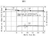
図5は、本発明の第1実施形態により、表面に酸化膜を形成したウエハを連続窒化処理した場合において、酸化膜中に注入された窒素含有量と、ウエハ間の窒素含有量の均一性を示す図である。図5において、左縦軸は、窒素ドーズ量、つまり酸化膜中に注入された窒素原子の数(1×10⁵/cm2)を示し、右縦軸は、ウエハ間の窒素ドーズ量の標準偏差(1σ)、横軸は、処理した製品用ウエハの処理番号である。処理番号は、処理した順に付されている。
また、51は、処理室201内を酸素のない無酸素雰囲気の状態、つまり、酸素の影響が無視できる状態にした後、表面に10nmの厚さの酸化膜(SiO2)を形成したシリコンウエハ8枚に対し、ウエハの温度を650℃、H2ガスとN2ガスの流量をそれぞれ、500sccm、処理室201内圧力を30Pa、筒状電極215に印加する高周波電力を800W、サセプタ217のバイアス電圧を本処理工程よりも大きい所定の値(このとき、インピーダンス可変機構274の可変コンデンサCの位置が40)、つまりウエハの電位を本処理工程よりも低い所定の値に制御して、120秒間、ダミー処理(事前処理)工程を行ったときの窒素ドーズ量である。
(3) Example Next, the example which performed the substrate processing process which combined the prior processing process and this processing process concerning a 1st embodiment is explained.
FIG. 5 shows the nitrogen content implanted into the oxide film and the uniformity of the nitrogen content between the wafers when the wafer having the oxide film formed on the surface is continuously nitrided according to the first embodiment of the present invention. FIG. In FIG. 5, the left vertical axis represents the nitrogen dose, that is, the number of nitrogen atoms implanted into the oxide film (1 × 10 5 / cm 2 ), and the right vertical axis represents the standard of the nitrogen dose between wafers. The deviation (1σ) and the horizontal axis are the processing numbers of the processed product wafers. Process numbers are given in the order of processing.
52は、そのダミー処理工程に引き続き、表面に10nmの厚さの酸化膜(SiO2)を形成したシリコンウエハに対し、ウエハの温度を650℃、H2ガスとN2ガスの流量をそれぞれ、1000sccm、処理室201内圧力を事前処理工程よりも高い100Pa、筒状電極215に印加する高周波電力を800W、サセプタ217のバイアス電圧を事前処理工程よりも小さい所定の値(このとき、インピーダンス可変機構274の可変コンデンサCの位置が16)、つまりウエハの電位を事前処理工程よりも高い所定の値に制御して、45秒間、本処理工程を行ったときの窒素ドーズ量である。
53は、本処理工程を行ったウエハ間の窒素ドーズ量の標準偏差(1σ)である。
52, following the dummy processing step, with respect to a silicon wafer having a 10 nm thick oxide film (SiO 2 ) formed on the surface, the wafer temperature is 650 ° C., and the flow rates of H 2 gas and N 2 gas are respectively 1000 sccm, the pressure in the
53 is a standard deviation (1σ) of the nitrogen dose amount between the wafers in which this processing step is performed.
このように、図5の例では、処理室201内を酸素のない無酸素雰囲気状態にした後、表面に10nmの厚さの酸化膜(SiO2)を形成したシリコンウエハ8枚でダミー処理(事前処理)を行い、その後、製品用ウエハを処理(本処理)したものである。なお、ダミー処理は5枚でも同程度の効果があることが確認されている。
図5に示すように、製品用ウエハ1〜25枚間における窒素ドーズ量の標準偏差(1σ)は、1.09%であり、ウエハ5〜8枚程度で第1実施形態に係るダミー処理(事前処理)を行うことにより、良好な結果が出ている。このように、従来よりもダミー処理の必要数を大きく低減できている。
また、上記したように、事前処理工程時の処理条件は、ウエハの温度が650℃、H2ガスとN2ガスの流量がそれぞれ、500sccm、処理室201内圧力が30Pa、高周波電力が800W、インピーダンス可変機構274の可変コンデンサCの位置が40、処理時間が120秒間であり、本処理工程の処理条件に対して、ウエハの温度が1倍、H2ガスとN2ガスの流量が0.5倍、処理室201内圧力が0.3倍、高周波電力が1倍、可変コンデンサCの位置が2.5倍、処理時間が2.7倍と簡単な倍率になっており、操作者が事前処理工程時の処理条件を設定することが容易となっている。事前処理工程時の処理条件は、操作部から入力することができる。
As described above, in the example of FIG. 5, after the inside of the
As shown in FIG. 5, the standard deviation (1σ) of the nitrogen dose amount between 1 to 25 product wafers is 1.09%, and dummy processing according to the first embodiment (about 5 to 8 wafers) is performed. Good results have been obtained by performing pre-processing. In this way, the required number of dummy processes can be greatly reduced as compared with the prior art.
Further, as described above, the processing conditions during the pre-processing step are as follows: the wafer temperature is 650 ° C., the flow rates of H 2 gas and N 2 gas are 500 sccm, the pressure in the
第1の実施形態によれば、少なくとも次の(1)〜(3)の効果を得ることができる。
(1)製品用ウエハ処理(本処理工程)の前に行うダミーウエハ処理(事前処理工程)において、製品用ウエハ処理よりも窒化力が高い条件で窒化処理を行うように構成したので、事前処理工程のプラズマ処理時における処理室内の酸素濃度を、従来よりも早く所定の一定濃度とすることができる。したがって、従来よりもダミーウエハの数を低減することができる。また、これにより、事前処理工程と本処理工程とを合わせた全体の基板処理工程の処理時間を低減することができる。
(2)ダミーウエハ処理(事前処理工程)と製品用ウエハ処理(本処理工程)をいずれも、N2ガスとH2ガスとを用いて行うように構成したので、本処理工程ではウエハ表面に形成された酸化膜を効率よく窒化することができ、事前処理工程では処理室内の酸素濃度を、本処理工程における酸素濃度に近づけることが容易となる。
(3)ダミーウエハ処理(事前処理工程)を、N2ガスとH2ガスとを用いて行うように構成したので、例えばN2ガスとO2ガスとを用いて行うように構成した場合に比べ、事前処理工程のプラズマ処理時における処理室内の酸素量を、ppmオーダー又はppbオーダーで微調整することが容易となる。
According to the first embodiment, at least the following effects (1) to (3) can be obtained.
(1) In the dummy wafer processing (pre-processing step) performed before the product wafer processing (main processing step), the nitriding processing is performed under a condition in which the nitriding power is higher than that of the product wafer processing. The oxygen concentration in the processing chamber during the plasma processing can be set to a predetermined constant concentration earlier than before. Therefore, the number of dummy wafers can be reduced as compared with the conventional case. In addition, this makes it possible to reduce the processing time of the entire substrate processing process including the preprocessing process and the main processing process.
(2) Since both the dummy wafer processing (pre-processing step) and the product wafer processing (main processing step) are performed using N 2 gas and H 2 gas, they are formed on the wafer surface in this processing step. The oxidized oxide film can be nitrided efficiently, and the oxygen concentration in the treatment chamber can be easily brought close to the oxygen concentration in the treatment step in the pretreatment step.
(3) Since the dummy wafer processing (pre-processing step) is configured to be performed using N 2 gas and H 2 gas, for example, compared to a case where the dummy wafer processing is performed using N 2 gas and O 2 gas. It becomes easy to finely adjust the oxygen amount in the processing chamber at the time of plasma processing in the pre-processing step on the order of ppm or ppb.
なお、上述した実施形態では、処理ガスとしての窒素含有ガスとしてN2ガスを用いたが、窒化作用のある他のガス、例えばアンモニアガス(NH3ガス)等を用いることもできる。また、H2ガスの代わりに、Arガス等を用いることもできる。
また、上述した実施形態では、サセプタ217に設けたインピーダンス調整電極217bをインピーダンス可変機構274により調整して、サセプタ217のバイアス電圧を所定の値に制御したが、インピーダンス調整電極をサセプタ217に設けずにサセプタ217のバイアス電圧を所定の値に制御するように構成してもよい。例えば、処理容器203全体にバイアスをかけるように構成してもよい。
In the above-described embodiment, the N 2 gas is used as the nitrogen-containing gas as the processing gas. However, other gases having a nitriding action, such as ammonia gas (NH 3 gas), can also be used. Also, instead of H 2 gas, it is also possible to use Ar gas or the like.
In the above-described embodiment, the
また、上述した実施形態では、サセプタ217の内部に設けたヒータ217cによってウエハ200を加熱するようにしていたが、本発明はこのような形態に限定されない。例えば、ヒータ217cに加えて、ランプ加熱ユニット280からも赤外線等を照射することでウエハ200を加熱するようにしてもよい。また、ヒータ217cとランプ加熱ユニット280とを併用することで、ヒータ217cのみを用いて加熱する場合と比較して、より短時間でウエハ200を昇温させることが可能である。また、ヒータ217cを設けずに、ランプ加熱ユニット280のみを用いてウエハ200を加熱するようにしてもよい。なお、ランプ加熱ユニット280は、信号線Gを通じて制御部121により制御するように構成されている。
また、上述の各実施形態では、ダミーウエハで事前処理を行った後、製品用ウエハで本処理を行ったが、製品用ウエハで事前処理を行うことも可能である。
In the above-described embodiment, the
Further, in each of the above-described embodiments, the pre-process is performed on the product wafer after the pre-process is performed on the dummy wafer. However, the pre-process may be performed on the product wafer.
また、上述の実施形態では、事前処理工程のDB基板昇温工程を、本処理工程のB基板昇温工程と同様の工程を行うことによって、処理室201内の雰囲気調整を行ったが、ウエハ200をサセプタ217の上方に、ウエハ突上げピン266によりウエハ200をサセプタ217から離して支持させて加熱するステップを省略することにより、DB基板昇温工程を短縮することができる。
Further, in the above-described embodiment, the atmosphere adjustment in the
また、上述した実施形態では、MMT装置として構成された基板処理装置100を用いて実施する場合を説明したが、本発明は、それに限らずその他の装置、例えばICP(Inductively Coupled Plasma)装置、ECR(Electron Cyclotron Resonance)装置を用いても実施可能である。
In the above-described embodiment, the case where the
(第2実施形態)
次に、第2実施形態について、図3を用いて説明する。図3は、本発明の第2実施形態に係る基板処理装置であるICP方式プラズマ処理装置300を示している。第2実施形態にかかる構成の詳細な説明は、第1実施形態と同様の機能を有する構成要件に同一の符号を付して省略する。また、ガス供給部についても図示を省略している。
第2実施形態に係るICP方式プラズマ処理装置300は、整合器272a、272b、高周波電源273a、273b及び誘電コイル315a,315bを介してそれぞれ電力が供給されることで、プラズマが生成される。誘電コイル315aは、処理容器203の天井側の外側に敷設されている。誘電コイル315bは、処理容器203の外周壁の外側に敷設されている。
(Second Embodiment)
Next, a second embodiment will be described with reference to FIG. FIG. 3 shows an ICP
The ICP
第2実施形態においても、事前処理や本処理において、水素原子や窒素原子を含む処理ガスをガス供給管232から、ガス導入口234を経由して処理室201内へ供給する。また、ガス供給と前後して、励起部である誘電コイル315a,315bへ高周波電力を流すと、電磁誘導により電界が生じる。この電界をエネルギーとして、供給された処理ガスをプラズマ状態として励起させて、活性種を生成することができる。
第2実施形態においても、本処理として製品用ウエハ上に形成された酸化膜の窒化処理を行う前に、事前処理として本発明のダミーウエハ処理を行う。
Also in the second embodiment, in pre-processing and main processing, a processing gas containing hydrogen atoms and nitrogen atoms is supplied from the
Also in the second embodiment, the dummy wafer process of the present invention is performed as a pre-process before the nitridation process of the oxide film formed on the product wafer is performed as the main process.
(第3実施形態)
次に、第3実施形態について、図4を用いて説明する。図4は、本発明の第3実施形態に係る基板処理装置であるECR方式プラズマ処理装置400を示している。第3実施形態にかかる構成の詳細な説明は、第1実施形態と同様の機能を有する構成要件に同一の符号を付して省略する。また、ガス供給部についても図示を省略している。
第3実施形態に係るECR方式プラズマ処理装置400は、マイクロ波を供給してプラズマを生成する整合器272b、高周波電源273b、マイクロ波導入管415a及び誘電コイル415bを備えている。マイクロ波導入管415aは、処理容器203の天井壁に敷設されている。誘電コイル415bは、処理容器203の外周壁の外側に敷設されている。
(Third embodiment)
Next, a third embodiment will be described with reference to FIG. FIG. 4 shows an ECR
The ECR
第3実施形態においても、事前処理や本処理において、水素原子や窒素原子を含む処理ガスをガス供給管232から、ガス導入口234を経由して処理室201内へ供給する。また、ガス供給と前後して、マイクロ波導入管415aへマイクロ波418aを導入し、マイクロ波418aを処理室201へ放射させる。このマイクロ波418aと、誘電コイル415bからの高周波電力とにより、供給された処理ガスをプラズマ状態として励起させ、活性種を生成することができる。なお、マイクロ波として、例えば可変周波数マイクロ波(VFM)、固定周波数マイクロ波(FFM)等を用いることができる。
第3実施形態においても、本処理として製品用ウエハ上に形成された酸化膜の窒化処理を行う前に、事前処理として本発明のダミーウエハ処理を行う。
Also in the third embodiment, in pre-processing and main processing, a processing gas containing hydrogen atoms and nitrogen atoms is supplied from the
Also in the third embodiment, the dummy wafer process of the present invention is performed as a pre-process before the nitridation process of the oxide film formed on the product wafer is performed as the main process.
この他、紫外線やレーザ光を照射することで、処理室内に導入されたガスを励起し、本処理としてウエハ上に形成された酸化膜の窒化処理を行う前に、事前処理として本発明のダミーウエハ処理を行うことができる。ただし、これらの場合、プラズマ処理に比べてガスの活性度が低いので、ダミーウエハ処理に要する時間は、プラズマ処理におけるダミーウエハ処理時間よりも長くなる。
また、RTP(Rapid Thermal Processing)装置等の加熱装置を用いて、処理室内に導入されたガスを熱エネルギーにより励起する場合は、処理室全体や処理室内の部材を加熱して高温にすると、酸素の付着量が減少するので、プラズマ処理に比べて不利になる。
In addition, the dummy wafer of the present invention is pre-processed before the gas introduced into the processing chamber is excited by irradiating ultraviolet rays or laser light, and the nitridation of the oxide film formed on the wafer is performed as the main process. Processing can be performed. However, in these cases, since the gas activity is lower than that in the plasma processing, the time required for the dummy wafer processing is longer than the dummy wafer processing time in the plasma processing.
In addition, when a gas introduced into the processing chamber is excited by thermal energy using a heating device such as an RTP (Rapid Thermal Processing) device, oxygen is increased by heating the entire processing chamber or a member in the processing chamber to a high temperature. This reduces the amount of adhesion of the material, which is disadvantageous compared to the plasma treatment.
なお、本発明は、上述の各実施形態に限定されるものではなく、その要旨を逸脱しない範囲で種々に変更が可能であることはいうまでもない。
また、上述の各実施形態では、ウエハに処理が施される場合について説明したが、処理対象はホトマスクやプリント配線基板、液晶パネル、コンパクトディスクおよび磁気ディスク等であってもよい。
The present invention is not limited to the above-described embodiments, and it goes without saying that various changes can be made without departing from the scope of the invention.
In each of the above-described embodiments, the case where processing is performed on a wafer has been described. However, a processing target may be a photomask, a printed wiring board, a liquid crystal panel, a compact disk, a magnetic disk, or the like.
本明細書には、少なくとも次の構成が含まれる。すなわち、
第1の構成は、
製品用基板を窒化処理する本処理工程と、製品用でないダミー基板を窒化処理する事前処理工程とを有し、前記本処理工程の前に前記事前処理工程を行う基板処理方法であって、
前記本処理工程は、
酸化膜が形成された製品用基板を処理室に搬入するステップと、
前記処理室内に窒素元素を含有する処理ガスを供給して前記処理室内を第1の圧力にするステップと、
前記処理室内に搬入された前記製品用基板を第1の電位にするステップと、
前記処理室内を前記第1の圧力とし、前記製品用基板を前記第1の電位とした状態で、前記処理室内に供給された処理ガスをプラズマ化して、前記製品用基板に形成された酸化膜を窒化処理するステップと、
前記処理室内を排気するステップと、
前記窒化処理された製品用基板を前記処理室から搬出するステップと、
を有し、
前記事前処理工程は、
酸化膜が形成されたダミー基板を前記処理室に搬入するステップと、
前記処理室内に窒素元素を含有する処理ガスを供給して前記処理室内を前記第1の圧力よりも低い第2の圧力にするステップと、
前記処理室内に搬入されたダミー基板を前記第1の電位よりも低い第2の電位にするステップと、
前記処理室内を前記第2の圧力とし、前記ダミー基板を前記第2の電位とした状態で、前記処理室内に供給された処理ガスをプラズマ化して、前記ダミー基板に形成された酸化膜を窒化処理するステップと、
前記処理室内を排気するステップと、
前記窒化処理されたダミー基板を前記処理室から搬出するステップと、
を有する基板処理方法。
The present specification includes at least the following configurations. That is,
The first configuration is
A substrate processing method comprising a main processing step of nitriding a product substrate and a preprocessing step of nitriding a dummy substrate not for product, wherein the preprocessing step is performed before the main processing step,
The main processing step includes
Carrying the product substrate on which the oxide film is formed into the processing chamber;
Supplying a processing gas containing nitrogen element to the processing chamber to bring the processing chamber to a first pressure;
Setting the product substrate carried into the processing chamber to a first potential;
An oxide film formed on the product substrate by converting the processing gas supplied into the processing chamber into plasma in a state where the processing chamber is at the first pressure and the product substrate is at the first potential. Nitriding
Exhausting the processing chamber;
Unloading the nitrided product substrate from the processing chamber;
Have
The pre-processing step includes
Carrying a dummy substrate on which an oxide film is formed into the processing chamber;
Supplying a processing gas containing nitrogen element into the processing chamber to bring the processing chamber to a second pressure lower than the first pressure;
Setting the dummy substrate carried into the processing chamber to a second potential lower than the first potential;
In a state where the processing chamber is at the second pressure and the dummy substrate is at the second potential, the processing gas supplied into the processing chamber is turned into plasma, and an oxide film formed on the dummy substrate is nitrided Processing steps;
Exhausting the processing chamber;
Unloading the nitrided dummy substrate from the processing chamber;
A substrate processing method.
第2の構成は、前記第1の構成の基板処理方法であって、
前記事前処理工程は、前記処理室内の雰囲気が所定値以上の酸素濃度になった場合に行われる基板処理方法。
The second configuration is the substrate processing method of the first configuration,
The pre-processing step is a substrate processing method performed when an atmosphere in the processing chamber has an oxygen concentration equal to or higher than a predetermined value.
第3の構成は、前記第1の構成又は第2の構成の基板処理方法であって、
前記事前処理工程において前記ダミー基板に形成された酸化膜を窒化処理する時間は、前記本処理工程において前記被処理基板に形成された酸化膜を窒化処理する時間よりも長い基板処理方法。
A third configuration is the substrate processing method of the first configuration or the second configuration,
The substrate processing method in which the time for nitriding the oxide film formed on the dummy substrate in the pre-processing step is longer than the time for nitriding the oxide film formed on the substrate to be processed in the main processing step.
第4の構成は、
酸化膜が形成された被処理基板を収容し、該被処理基板に形成された酸化膜を窒化処理する処理室と、
前記窒化処理を行う処理ガスを前記処理室内へ供給するガス供給部と、
前記処理室内のガスを排出するガス排気部と、
前記処理室内へ供給された前記処理ガスをプラズマ化するプラズマ生成部と、
前記処理室内へ搬入された被処理基板の電位を変更する基板電位変更部と、
前記ガス供給部と前記ガス排気部と前記プラズマ生成部と前記基板電位変更部とを制御する制御部とを備え、
前記制御部は、
酸化膜が形成された被処理基板を前記処理室内へ搬入し、その後、前記ガス供給部から前記処理ガスを前記処理室内へ供給して、前記処理室内を第1の圧力にするとともに、前記処理室内に搬入された前記被処理基板を前記基板電位変更部により第1の電位にし、前記処理室内を前記第1の圧力とし前記被処理基板を前記第1の電位とした状態で、前記処理室内に供給された前記処理ガスを前記プラズマ生成部によりプラズマ化して、前記被処理基板に形成された酸化膜を窒化処理し、その後、前記処理室内のガスを前記ガス排気部により排出した後、前記被処理基板を前記処理室内から搬出する第1の被処理基板処理工程と、
酸化膜が形成された被処理基板を前記処理室内へ搬入し、その後、前記ガス供給部から前記処理ガスを前記処理室内へ供給して、前記処理室内を前記第1の圧力よりも低い第2の圧力にするとともに、前記処理室内に搬入された前記被処理基板を前記基板電位変更部により前記第1の電位よりも低い第2の電位にし、前記処理室内を前記第2の圧力とし前記被処理基板を前記第2の電位とした状態で、前記処理室内に供給された前記処理ガスを前記プラズマ生成部によりプラズマ化して、前記被処理基板に形成された酸化膜を窒化処理し、その後、前記処理室内のガスを前記ガス排気部により排出した後、前記被処理基板を前記処理室内から搬出する第2の被処理基板処理工程と、
を行い、前記第1の被処理基板処理工程の前に前記第2の被処理基板処理工程を行うよう制御する基板処理装置。
The fourth configuration is
A processing chamber for accommodating a substrate to be processed on which an oxide film is formed, and nitriding the oxide film formed on the substrate to be processed;
A gas supply unit for supplying a processing gas for performing the nitriding treatment into the processing chamber;
A gas exhaust unit for exhausting the gas in the processing chamber;
A plasma generation unit that converts the processing gas supplied into the processing chamber into plasma;
A substrate potential changing unit for changing the potential of the substrate to be processed carried into the processing chamber;
A control unit for controlling the gas supply unit, the gas exhaust unit, the plasma generation unit, and the substrate potential changing unit;
The controller is
The substrate to be processed on which the oxide film is formed is carried into the processing chamber, and then the processing gas is supplied from the gas supply unit into the processing chamber to bring the processing chamber to a first pressure, and the processing The substrate to be processed carried into the chamber is set to a first potential by the substrate potential changing unit, the processing chamber is set to the first pressure, and the substrate to be processed is set to the first potential. The processing gas supplied to the substrate is converted into plasma by the plasma generation unit, an oxide film formed on the substrate to be processed is nitrided, and then the gas in the processing chamber is exhausted by the gas exhaust unit, A first substrate processing step for unloading the substrate to be processed from the processing chamber;
The substrate to be processed on which the oxide film is formed is carried into the processing chamber, and then the processing gas is supplied from the gas supply unit into the processing chamber, and the processing chamber is supplied with a second pressure lower than the first pressure. And the substrate potential changing unit sets the substrate potential changing unit to a second potential lower than the first potential, and the processing chamber is set to the second pressure. In a state where the processing substrate is at the second potential, the processing gas supplied into the processing chamber is turned into plasma by the plasma generation unit, and an oxide film formed on the processing substrate is nitrided, A second processing substrate processing step of discharging the processing substrate from the processing chamber after exhausting the gas in the processing chamber by the gas exhaust unit;
And a substrate processing apparatus that controls to perform the second substrate processing step before the first substrate processing step.
第5の構成は、
製品用基板を窒化処理する本処理工程と、製品用でないダミー基板を窒化処理する事前処理工程とを有し、前記本処理工程の前に前記事前処理工程を行う半導体装置の製造方法であって、
前記本処理工程は、
酸化膜が形成された製品用基板を処理室に搬入するステップと、
前記処理室内に窒素元素を含有する処理ガスを供給して前記処理室内を第1の圧力にするステップと、
前記処理室内に搬入された前記製品用基板を第1の電位にするステップと、
前記処理室内を前記第1の圧力とし、前記製品用基板を前記第1の電位とした状態で、前記処理室内に供給された処理ガスをプラズマ化して、前記製品用基板に形成された酸化膜を窒化処理するステップと、
前記処理室内を排気するステップと、
前記窒化処理された製品用基板を前記処理室から搬出するステップと、
を有し、
前記事前処理工程は、
酸化膜が形成されたダミー基板を処理室に搬入するステップと、
前記処理室内に窒素元素を含有する処理ガスを供給して前記処理室内を前記第1の圧力よりも低い第2の圧力にするステップと、
前記処理室内に搬入されたダミー基板を前記第1の電位よりも低い第2の電位にするステップと、
前記処理室内を前記第2の圧力とし、前記ダミー基板を前記第2の電位とした状態で、前記処理室内に供給された処理ガスをプラズマ化して、前記ダミー基板に形成された酸化膜を窒化処理するステップと、
前記処理室内を排気するステップと、
前記窒化処理されたダミー基板を前記処理室から搬出するステップと、
を有する半導体装置の製造方法。
The fifth configuration is
A method for manufacturing a semiconductor device, comprising: a main processing step of nitriding a product substrate; and a preprocessing step of nitriding a dummy substrate not for product, wherein the preprocessing step is performed before the main processing step. And
The main processing step includes
Carrying the product substrate on which the oxide film is formed into the processing chamber;
Supplying a processing gas containing nitrogen element to the processing chamber to bring the processing chamber to a first pressure;
Setting the product substrate carried into the processing chamber to a first potential;
An oxide film formed on the product substrate by converting the processing gas supplied into the processing chamber into plasma in a state where the processing chamber is at the first pressure and the product substrate is at the first potential. Nitriding
Exhausting the processing chamber;
Unloading the nitrided product substrate from the processing chamber;
Have
The pre-processing step includes
Carrying a dummy substrate on which an oxide film is formed into a processing chamber;
Supplying a processing gas containing nitrogen element into the processing chamber to bring the processing chamber to a second pressure lower than the first pressure;
Setting the dummy substrate carried into the processing chamber to a second potential lower than the first potential;
In a state where the processing chamber is at the second pressure and the dummy substrate is at the second potential, the processing gas supplied into the processing chamber is turned into plasma, and an oxide film formed on the dummy substrate is nitrided Processing steps;
Exhausting the processing chamber;
Unloading the nitrided dummy substrate from the processing chamber;
A method for manufacturing a semiconductor device comprising:
第6の構成は、
被処理基板を窒化処理する第1の処理工程と第2の処理工程とを有し、前記第1の処理工程の前に前記第2の処理工程を行う基板処理方法であって、
前記第1の処理工程は、
酸化膜が形成された被処理基板を処理室に搬入するステップと、
前記処理室内に窒素元素を含有する処理ガスを供給して前記処理室内を第1の圧力にするステップと、
前記処理室内に搬入された前記被処理基板を第1の電位にするステップと、
前記処理室内を前記第1の圧力とし、前記被処理基板を前記第1の電位とした状態で、前記処理室内に供給された処理ガスをプラズマ化して、前記被処理基板に形成された酸化膜を窒化処理するステップと、
前記処理室内を排気するステップと、
前記窒化処理された被処理基板を前記処理室から搬出するステップと、
を有し、
前記第2の処理工程は、
酸化膜が形成された被処理基板を処理室に搬入するステップと、
前記処理室内に窒素元素を含有する処理ガスを供給して前記処理室内を前記第1の圧力よりも低い第2の圧力にするステップと、
前記処理室内に搬入された被処理基板を前記第1の電位よりも低い第2の電位にするステップと、
前記処理室内を前記第2の圧力とし、前記被処理基板を前記第2の電位とした状態で、前記処理室内に供給された処理ガスをプラズマ化して、前記被処理基板に形成された酸化膜を窒化処理するステップと、
前記処理室内を排気するステップと、
前記窒化処理された被処理基板を前記処理室から搬出するステップと、
を有する基板処理方法。
The sixth configuration is
A substrate processing method having a first processing step and a second processing step for nitriding a substrate to be processed, and performing the second processing step before the first processing step,
The first processing step includes
Carrying a substrate to be processed on which an oxide film is formed into a processing chamber;
Supplying a processing gas containing nitrogen element to the processing chamber to bring the processing chamber to a first pressure;
Setting the substrate to be processed carried into the processing chamber to a first potential;
An oxide film formed on the substrate to be processed by converting the processing gas supplied into the processing chamber into plasma with the processing chamber at the first pressure and the substrate to be processed at the first potential. Nitriding
Exhausting the processing chamber;
Unloading the nitrided substrate to be processed from the processing chamber;
Have
The second processing step includes
Carrying a substrate to be processed on which an oxide film is formed into a processing chamber;
Supplying a processing gas containing nitrogen element into the processing chamber to bring the processing chamber to a second pressure lower than the first pressure;
Setting the substrate to be processed carried into the processing chamber to a second potential lower than the first potential;
An oxide film formed on the substrate to be processed by converting the processing gas supplied into the processing chamber into plasma while the processing chamber is at the second pressure and the substrate to be processed is at the second potential. Nitriding
Exhausting the processing chamber;
Unloading the nitrided substrate to be processed from the processing chamber;
A substrate processing method.
第7の構成は、
製品用基板を窒化処理する本処理工程と、製品用でないダミー基板を窒化処理する事前処理工程とを有し、前記本処理工程の前に前記事前処理工程を行う基板処理方法であって、
前記本処理工程は、
酸化膜が形成された製品用基板を処理室に搬入するステップと、
前記処理室内に窒素元素を含有する処理ガスを供給して前記処理室内を第1の圧力にするステップと、
前記処理室内に搬入された前記製品用基板を第1の電位にするステップと、
前記処理室内を前記第1の圧力とし、前記製品用基板を前記第1の電位とした状態で、前記処理室内に供給された処理ガスを第1の電力によりプラズマ化して、前記製品用基板に形成された酸化膜を第1の時間窒化処理するステップと、
前記処理室内を排気するステップと、
前記窒化処理された製品用基板を前記処理室から搬出するステップと、
を有し、
前記事前処理工程は、
酸化膜が形成されたダミー基板を前記処理室に搬入するステップと、
前記処理室内に窒素元素を含有する処理ガスを供給して前記処理室内を第2の圧力にするステップと、
前記処理室内に搬入されたダミー基板を第2の電位にするステップと、
前記処理室内を前記第2の圧力とし、前記ダミー基板を前記第2の電位とした状態で、前記処理室内に供給された処理ガスを第2の電力によりプラズマ化して、前記ダミー基板に形成された酸化膜を第2の時間窒化処理するステップと、
前記処理室内を排気するステップと、
前記窒化処理されたダミー基板を前記処理室から搬出するステップと、
を有し、
前記第2の圧力が前記第1の圧力よりも低いか、又は、前記第2の電位が前記第1の電位よりも低いか、又は、前記第2の電力が前記第1の電力よりも大きいか、又は、前記第2の時間が前記第1の時間よりも長い基板処理方法。
The seventh configuration is
A substrate processing method comprising a main processing step of nitriding a product substrate and a preprocessing step of nitriding a dummy substrate not for product, wherein the preprocessing step is performed before the main processing step,
The main processing step includes
Carrying the product substrate on which the oxide film is formed into the processing chamber;
Supplying a processing gas containing nitrogen element to the processing chamber to bring the processing chamber to a first pressure;
Setting the product substrate carried into the processing chamber to a first potential;
In a state where the processing chamber is at the first pressure and the product substrate is at the first potential, the processing gas supplied into the processing chamber is turned into plasma by a first power to form the product substrate. Nitriding the formed oxide film for a first time;
Exhausting the processing chamber;
Unloading the nitrided product substrate from the processing chamber;
Have
The pre-processing step includes
Carrying a dummy substrate on which an oxide film is formed into the processing chamber;
Supplying a processing gas containing nitrogen element to the processing chamber to bring the processing chamber to a second pressure;
Setting the dummy substrate carried into the processing chamber to a second potential;
In the state where the processing chamber is at the second pressure and the dummy substrate is at the second potential, the processing gas supplied into the processing chamber is turned into plasma by a second electric power to be formed on the dummy substrate. Nitriding the oxidized film for a second time;
Exhausting the processing chamber;
Unloading the nitrided dummy substrate from the processing chamber;
Have
The second pressure is lower than the first pressure, or the second potential is lower than the first potential, or the second power is higher than the first power. Alternatively, the substrate processing method wherein the second time is longer than the first time.
第8の構成は、
酸化膜が形成された被処理基板を収容し、該被処理基板に形成された酸化膜を窒化処理する処理室と、
前記窒化処理を行う処理ガスを前記処理室内へ供給するガス供給部と、
前記処理室内のガスを排出するガス排気部と、
前記処理室内へ供給された前記処理ガスをプラズマ化するプラズマ生成部と、
前記処理室内へ搬入された被処理基板の電位を変更する基板電位変更部と、
前記ガス供給部と前記ガス排気部と前記プラズマ生成部と前記基板電位変更部とを制御する制御部とを備え、
前記制御部は、
酸化膜が形成された被処理基板を前記処理室内へ搬入し、その後、前記ガス供給部から前記処理ガスを前記処理室内へ供給して、前記処理室内を第1の圧力にするとともに、前記処理室内に搬入された前記被処理基板を前記基板電位変更部により第1の電位にし、前記処理室内を前記第1の圧力とし前記被処理基板を前記第1の電位とした状態で、前記処理室内に供給された前記処理ガスを前記プラズマ生成部により第1の電力でプラズマ化して、前記被処理基板に形成された酸化膜を第1の時間窒化処理し、その後、前記処理室内のガスを前記ガス排気部により排出した後、前記被処理基板を前記処理室内から搬出する第1の被処理基板処理工程と、
酸化膜が形成された被処理基板を前記処理室内へ搬入し、その後、前記ガス供給部から前記処理ガスを前記処理室内へ供給して、前記処理室内を第2の圧力にするとともに、前記処理室内に搬入された前記被処理基板を前記基板電位変更部により第2の電位にし、前記処理室内を前記第2の圧力とし前記被処理基板を前記第2の電位とした状態で、前記処理室内に供給された前記処理ガスを前記プラズマ生成部により第2の電力でプラズマ化して、前記被処理基板に形成された酸化膜を第2の時間窒化処理し、その後、前記処理室内のガスを前記ガス排気部により排出した後、前記被処理基板を前記処理室内から搬出する第2の被処理基板処理工程と、
を行い、前記第1の被処理基板処理工程の前に前記第2の被処理基板処理工程を行うとともに、前記第2の圧力が前記第1の圧力よりも低いか、又は、前記第2の電位が前記第1の電位よりも低いか、又は、前記第2の電力が前記第1の電力よりも大きいか、又は、前記第2の時間が前記第1の時間よりも長いか、少なくともいずれか1つを行うよう制御する基板処理装置。
The eighth configuration is
A processing chamber for accommodating a substrate to be processed on which an oxide film is formed, and nitriding the oxide film formed on the substrate to be processed;
A gas supply unit for supplying a processing gas for performing the nitriding treatment into the processing chamber;
A gas exhaust unit for exhausting the gas in the processing chamber;
A plasma generation unit that converts the processing gas supplied into the processing chamber into plasma;
A substrate potential changing unit for changing the potential of the substrate to be processed carried into the processing chamber;
A control unit for controlling the gas supply unit, the gas exhaust unit, the plasma generation unit, and the substrate potential changing unit;
The controller is
The substrate to be processed on which the oxide film is formed is carried into the processing chamber, and then the processing gas is supplied from the gas supply unit into the processing chamber to bring the processing chamber to a first pressure, and the processing The substrate to be processed carried into the chamber is set to a first potential by the substrate potential changing unit, the processing chamber is set to the first pressure, and the substrate to be processed is set to the first potential. The processing gas supplied to the substrate is turned into plasma with a first power by the plasma generation unit, and the oxide film formed on the substrate to be processed is subjected to nitriding treatment for a first time. A first processing substrate processing step of discharging the processing substrate from the processing chamber after exhausting by the gas exhaust unit;
The substrate to be processed on which the oxide film is formed is carried into the processing chamber, and then the processing gas is supplied from the gas supply unit into the processing chamber to bring the processing chamber to a second pressure, and the processing The substrate to be processed carried into the chamber is set to a second potential by the substrate potential changing unit, the processing chamber is set to the second pressure, and the substrate to be processed is set to the second potential. The processing gas supplied to the substrate is turned into plasma with the second power by the plasma generation unit, and the oxide film formed on the substrate to be processed is subjected to nitriding treatment for a second time. A second processing substrate processing step for discharging the processing substrate from the processing chamber after being discharged by the gas exhaust unit;
And the second substrate processing step is performed before the first substrate processing step, and the second pressure is lower than the first pressure or the second substrate processing step is performed. The potential is lower than the first potential, or the second power is greater than the first power, or the second time is longer than the first time. A substrate processing apparatus which controls to perform one of them.
第9の構成は、
前記第1ないし第3の構成、あるいは前記第6又は第7の構成のいずれかの基板処理方法を実行させるためのプログラムが記録された記録媒体。
The ninth configuration is
A recording medium on which a program for executing the substrate processing method of any one of the first to third configurations or the sixth or seventh configuration is recorded.
第10の構成は、
前記第5の構成の半導体装置の製造方法を実行させるためのプログラムが記録された記録媒体。
The tenth configuration is
A recording medium on which a program for executing the semiconductor device manufacturing method of the fifth configuration is recorded.
100…MMT装置、121…コントローラ、122…操作部、123…表示部、124…演算部、125…記録部、200…ウエハ、201…処理室、202…処理炉、203…処理容器、203b…ガスケット、210…上側容器、211…下側容器、215…筒状電極、216a…上側磁石、216b…下側磁石、217…サセプタ、217a…貫通孔、217c…ヒータ、217b…インピーダンス調整電極、223…遮蔽板、224…プラズマ生成領域、231a…ガス排気管、231b…ガス排気管、232…ガス供給管、232a…水素含有ガス供給管、232b…窒素含有ガス供給管、233…蓋体、234…ガス導入口、235…ガス排気口、236…シャワーヘッド、237…バッファ室、238…開口、239…ガス吹出口、240…遮蔽プレート、242…APC、243a…主要バルブ、243b…スロー排気バルブ、244…ゲートバルブ、246a…ターボ分子ポンプ、246b…ドライポンプ、250a…H2ガス供給源、250b…N2ガス供給源、252a…マスフローコントローラ、252b…マスフローコントローラ、253a…バルブ、253b…バルブ、254…バルブ、266…ウエハ突き上げピン、268…サセプタ昇降機構、272…整合器、272a…整合器、272b…整合器、273…高周波電源、273a…高周波電源、273b…高周波電源、274…インピーダンス可変機構、278…光透過窓、280…ランプ加熱ユニット、300…ICP方式プラズマ処理装置、315a…放電コイル、315b…放電コイル、400…ECR方式プラズマ処理装置、415a…マイクロ波導入管、415b…誘電コイル、418a…マイクロ波。
DESCRIPTION OF
Claims (12)
前記本処理工程は、
酸化膜が形成された前記製品用基板を処理室に収容する工程と、
前記処理室内に窒素を含有する処理ガスを供給する工程と、
前記処理室内の圧力を第1圧力、前記製品用基板の電位を第1電位にした状態で前記処理ガスをプラズマ励起して、前記製品用基板に形成された前記酸化膜を窒化処理する工程と、
前記製品用基板を前記処理室から搬出する工程と、を含み、
前記事前処理工程は、
酸化膜が形成された前記ダミー基板を前記処理室に収容する工程と、
前記処理室内に窒素を含有する前記処理ガスを供給する工程と、
前記処理室内の圧力を前記第1圧力よりも低い第2圧力、前記ダミー基板の電位を前記第1電位よりも低い第2電位にした状態で前記処理ガスをプラズマ励起して、前記ダミー基板に形成された前記酸化膜から放出される酸素原子を前記処理室の内壁に付着させる工程と、
前記ダミー基板を前記処理室から搬出する工程と、を含む、
半導体装置の製造方法。 A method for manufacturing a semiconductor device, comprising: a main processing step of nitriding a product substrate; and a preprocessing step of nitriding a dummy substrate not for product, wherein the preprocessing step is performed before the main processing step. And
The main processing step includes
Storing the product substrate on which the oxide film is formed in a processing chamber;
Supplying a processing gas containing nitrogen into the processing chamber ;
Nitriding the oxide film formed on the product substrate by plasma- exciting the process gas with the pressure in the processing chamber set to a first pressure and the product substrate potential set to a first potential; ,
Unloading the product substrate from the processing chamber,
The pre-processing step includes
Accommodating the dummy substrate on which the oxide film is formed in the processing chamber;
Supplying the processing gas containing nitrogen into the processing chamber;
The process gas is plasma- excited in a state where the pressure in the processing chamber is set to a second pressure lower than the first pressure, and the potential of the dummy substrate is set to a second potential lower than the first potential. Attaching oxygen atoms released from the formed oxide film to the inner wall of the processing chamber ;
Unloading the dummy substrate from the processing chamber,
A method for manufacturing a semiconductor device.
請求項1に記載の半導体装置の製造方法。 The pretreatment step is performed when the atmosphere in the treatment chamber has an oxygen concentration different from a predetermined value.
A method for manufacturing a semiconductor device according to claim 1 .
請求項1又は2に記載の半導体装置の製造方法。 The time for plasma excitation of the processing gas in the pre-processing step is longer than the time for plasma excitation of the processing gas in the main processing step.
A method for manufacturing a semiconductor device according to claim 1 .
請求項1乃至3のいずれかに記載の半導体装置の製造方法。 The magnitude of the high-frequency power applied for plasma- exciting the processing gas in the pre-processing step is larger than the magnitude of the high-frequency power applied for plasma- exciting the processing gas in the main processing step,
The method of manufacturing a semiconductor device according to any one of claims 1 to 3.
基板を前記処理室に対して搬入及び搬出する搬送機構と、
前記処理室に収容された基板に窒素を含有する処理ガスを供給するガス供給部と、
前記処理ガスを励起するプラズマ生成部と、
前記基板の電位を変更する基板電位変更部と、
製品用でないダミー基板を窒化処理する事前処理工程の後に、製品用基板を窒化処理する本処理工程を行うように、前記ガス供給部、前記プラズマ生成部、及び前記基板電位変更部を制御するよう構成される制御部と、を有し、
前記本処理工程は、酸化膜が形成された前記製品用基板を前記処理室に収容する工程と、前記処理室内に前記処理ガスを供給する工程と、前記処理室内の圧力を第1圧力、前記製品用基板の電位を第1電位にした状態で前記処理ガスをプラズマ励起して、前記製品用基板に形成された前記酸化膜を窒化処理する工程と、前記製品用基板を前記処理室から搬出する工程と、を含み、
前記事前処理工程は、酸化膜が形成された前記ダミー基板を前記処理室に収容する工程と、前記処理室内に前記処理ガスを供給する工程と、前記処理室内の圧力を前記第1圧力よりも低い第2圧力、前記ダミー基板の電位を前記第1電位よりも低い第2電位にした状態で前記処理ガスをプラズマ励起して、前記ダミー基板に形成された前記酸化膜から放出される酸素原子を前記処理室の内壁に付着させる工程と、前記ダミー基板を前記処理室から搬出する工程と、を含む、
基板処理装置。 A processing chamber for accommodating a substrate on which an oxide film is formed;
A transport mechanism for carrying the substrate into and out of the processing chamber;
A gas supply unit for supplying a processing gas containing nitrogen to the substrate housed in the processing chamber;
A plasma generator for exciting the processing gas;
A substrate potential changing unit for changing the potential of the substrate;
The gas supply unit, the plasma generation unit, and the substrate potential changing unit are controlled so as to perform the main processing step of nitriding the product substrate after the pre-processing step of nitriding the dummy substrate not for product. A control unit configured,
The main processing step includes the step of accommodating the product substrate on which the oxide film is formed in the processing chamber, the step of supplying the processing gas into the processing chamber, the pressure in the processing chamber being a first pressure, Nitriding the oxide film formed on the product substrate by plasma- exciting the processing gas with the potential of the product substrate set to the first potential; and unloading the product substrate from the processing chamber Including the steps of:
The pre-processing step includes a step of accommodating the dummy substrate on which the oxide film is formed in the processing chamber, a step of supplying the processing gas into the processing chamber, and a pressure in the processing chamber from the first pressure. Oxygen released from the oxide film formed on the dummy substrate by plasma- exciting the process gas with the second pressure being lower and the dummy substrate potential being a second potential lower than the first potential. Including attaching atoms to the inner wall of the processing chamber, and unloading the dummy substrate from the processing chamber.
Substrate processing equipment.
請求項5に記載の基板処理装置。 The control unit controls the gas supply unit, the plasma generation unit, and the substrate potential changing unit so that the pretreatment process is performed when an atmosphere in the processing chamber has an oxygen concentration different from a predetermined value. Configured to
The substrate processing apparatus according to claim 5 .
請求項5又は6に記載の基板処理装置。 The control unit is configured to control the plasma generation unit so that a time for plasma excitation of the processing gas in the preliminary processing step is longer than a time for plasma excitation of the processing gas in the main processing step. The
The substrate processing apparatus according to claim 5 or 6 .
請求項5乃至7のいずれかに記載の基板処理装置。 The control unit is configured such that the magnitude of the high-frequency power applied to plasma- excite the processing gas in the pre-processing step is equal to the high-frequency power applied to plasma- excite the processing gas in the main processing step. Configured to control the plasma generator to be larger than the size,
The substrate processing apparatus according to claim 5 .
前記本処理手順は、
酸化膜が形成された前記製品用基板を処理室に収容する手順と、
前記処理室内に窒素を含有する処理ガスを供給する手順と、
前記処理室内の圧力を第1圧力、前記製品用基板の電位を第1電位にした状態で前記処理ガスをプラズマ励起して、前記製品用基板に形成された前記酸化膜を窒化処理する手順と、
前記製品用基板を前記処理室から搬出する手順と、を含み、
前記事前処理手順は、
酸化膜が形成された前記ダミー基板を前記処理室に収容する手順と、
前記処理室内に窒素を含有する前記処理ガスを供給する手順と、
前記処理室内の圧力を前記第1圧力よりも低い第2圧力、前記ダミー基板の電位を前記第1電位よりも低い第2電位にした状態で前記処理ガスをプラズマ励起して、前記ダミー基板に形成された前記酸化膜から放出される酸素原子を前記処理室の内壁に付着させる手順と、
前記ダミー基板を前記処理室から搬出する手順と、を含む、
プログラム。 A main processing procedure for nitriding a product substrate and a preprocessing procedure for nitriding a non-product dummy substrate, and causing the substrate processing apparatus to execute the preprocessing procedure by a computer before the main processing procedure. A program,
The processing procedure is as follows:
A procedure for accommodating the product substrate on which the oxide film is formed in a processing chamber;
Supplying a processing gas containing nitrogen into the processing chamber ;
Nitriding the oxide film formed on the product substrate by plasma- exciting the processing gas with the pressure in the processing chamber set to a first pressure and the product substrate potential set to the first potential; ,
A procedure for unloading the product substrate from the processing chamber,
The pre-processing procedure is as follows:
A procedure for accommodating the dummy substrate on which the oxide film is formed in the processing chamber;
Supplying the processing gas containing nitrogen into the processing chamber;
The process gas is plasma- excited in a state where the pressure in the processing chamber is set to a second pressure lower than the first pressure, and the potential of the dummy substrate is set to a second potential lower than the first potential. A procedure for attaching oxygen atoms released from the formed oxide film to the inner wall of the processing chamber ;
And a procedure for unloading the dummy substrate from the processing chamber.
program.
請求項9に記載のプログラム。 The pretreatment procedure is performed when the atmosphere in the processing chamber has an oxygen concentration different from a predetermined value.
The program according to claim 9 .
請求項9又は10に記載のプログラム。 The time for plasma- exciting the processing gas in the pre-processing procedure is longer than the time for plasma- exciting the processing gas in the main processing procedure ,
The program according to claim 9 or 10 .
請求項9乃至11のいずれかに記載のプログラム。The program according to any one of claims 9 to 11.
Priority Applications (3)
| Application Number | Priority Date | Filing Date | Title |
|---|---|---|---|
| JP2012068850A JP6022785B2 (en) | 2012-03-26 | 2012-03-26 | Semiconductor device manufacturing method, substrate processing apparatus, and program |
| US13/826,599 US9257271B2 (en) | 2012-03-26 | 2013-03-14 | Semiconductor device manufacturing method, substrate processing apparatus, and non-transitory recording medium |
| KR1020130031637A KR101464867B1 (en) | 2012-03-26 | 2013-03-25 | Semiconductor device manufacturing method, substrate processing apparatus, and recording medium |
Applications Claiming Priority (1)
| Application Number | Priority Date | Filing Date | Title |
|---|---|---|---|
| JP2012068850A JP6022785B2 (en) | 2012-03-26 | 2012-03-26 | Semiconductor device manufacturing method, substrate processing apparatus, and program |
Publications (3)
| Publication Number | Publication Date |
|---|---|
| JP2013201300A JP2013201300A (en) | 2013-10-03 |
| JP2013201300A5 JP2013201300A5 (en) | 2015-04-23 |
| JP6022785B2 true JP6022785B2 (en) | 2016-11-09 |
Family
ID=49212224
Family Applications (1)
| Application Number | Title | Priority Date | Filing Date |
|---|---|---|---|
| JP2012068850A Active JP6022785B2 (en) | 2012-03-26 | 2012-03-26 | Semiconductor device manufacturing method, substrate processing apparatus, and program |
Country Status (3)
| Country | Link |
|---|---|
| US (1) | US9257271B2 (en) |
| JP (1) | JP6022785B2 (en) |
| KR (1) | KR101464867B1 (en) |
Families Citing this family (4)
| Publication number | Priority date | Publication date | Assignee | Title |
|---|---|---|---|---|
| JP2014116545A (en) * | 2012-12-12 | 2014-06-26 | Tokyo Electron Ltd | Substrate processing apparatus |
| KR20160144307A (en) * | 2015-06-08 | 2016-12-16 | 울트라테크 인크. | Microchamber Laser Processing Systems and Methods Using Localized Process-Gas Atmosphere |
| JP6811638B2 (en) * | 2017-02-14 | 2021-01-13 | 株式会社Screenホールディングス | Substrate processing method and its equipment |
| US10544519B2 (en) * | 2017-08-25 | 2020-01-28 | Aixtron Se | Method and apparatus for surface preparation prior to epitaxial deposition |
Family Cites Families (18)
| Publication number | Priority date | Publication date | Assignee | Title |
|---|---|---|---|---|
| JP2889191B2 (en) | 1996-07-31 | 1999-05-10 | 芝浦メカトロニクス株式会社 | Dry etching method |
| JP3902000B2 (en) * | 2001-12-12 | 2007-04-04 | 株式会社ルネサステクノロジ | Method for manufacturing semiconductor device, method for determining film formation time |
| JP2006005287A (en) | 2004-06-21 | 2006-01-05 | Hitachi Kokusai Electric Inc | Substrate treatment method |
| US7176138B2 (en) * | 2004-10-21 | 2007-02-13 | Taiwan Semiconductor Manufacturing Co., Ltd. | Selective nitride liner formation for shallow trench isolation |
| JP5371425B2 (en) * | 2005-06-02 | 2013-12-18 | アプライド マテリアルズ インコーポレイテッド | Method and apparatus for incorporating nitrogen into an oxide film |
| JP5461759B2 (en) | 2006-03-22 | 2014-04-02 | 東京エレクトロン株式会社 | Plasma processing apparatus, plasma processing method, and storage medium |
| US7883632B2 (en) | 2006-03-22 | 2011-02-08 | Tokyo Electron Limited | Plasma processing method |
| JP5425361B2 (en) * | 2006-07-28 | 2014-02-26 | 東京エレクトロン株式会社 | Plasma surface treatment method, plasma treatment method, and plasma treatment apparatus |
| CN101681836B (en) * | 2007-05-29 | 2011-11-16 | 东京毅力科创株式会社 | Method for pretreating inner space of chamber in plasma nitridation, plasma processing method and plasma processing apparatus |
| JP2009260091A (en) * | 2008-04-18 | 2009-11-05 | Hitachi High-Technologies Corp | Seasoning method of plasma treatment device |
| JP2011077321A (en) * | 2009-09-30 | 2011-04-14 | Tokyo Electron Ltd | Selective plasma nitriding method, and plasma nitriding device |
| JP2011165743A (en) * | 2010-02-05 | 2011-08-25 | Hitachi Kokusai Electric Inc | Method of manufacturing semiconductor-device |
| JP5546921B2 (en) | 2010-03-26 | 2014-07-09 | 株式会社日立国際電気 | Substrate processing apparatus and semiconductor device manufacturing method |
| JP2011216593A (en) * | 2010-03-31 | 2011-10-27 | Tokyo Electron Ltd | Plasma nitriding treatment method |
| CN102725835A (en) * | 2010-03-31 | 2012-10-10 | 东京毅力科创株式会社 | Plasma nitridization method |
| WO2011125705A1 (en) * | 2010-03-31 | 2011-10-13 | 東京エレクトロン株式会社 | Plasma nitriding treatment method and plasma nitriding treatment device. |
| US8809206B2 (en) * | 2011-02-07 | 2014-08-19 | Spansion Llc | Patterned dummy wafers loading in batch type CVD |
| US8569143B2 (en) * | 2011-06-23 | 2013-10-29 | GlobalFoundries, Inc. | Methods of fabricating a semiconductor IC having a hardened shallow trench isolation (STI) |
-
2012
- 2012-03-26 JP JP2012068850A patent/JP6022785B2/en active Active
-
2013
- 2013-03-14 US US13/826,599 patent/US9257271B2/en not_active Expired - Fee Related
- 2013-03-25 KR KR1020130031637A patent/KR101464867B1/en active IP Right Grant
Also Published As
| Publication number | Publication date |
|---|---|
| KR101464867B1 (en) | 2014-11-25 |
| KR20130109062A (en) | 2013-10-07 |
| US9257271B2 (en) | 2016-02-09 |
| US20130252433A1 (en) | 2013-09-26 |
| JP2013201300A (en) | 2013-10-03 |
Similar Documents
| Publication | Publication Date | Title |
|---|---|---|
| US9472424B2 (en) | Substrate processing apparatus and a method of manufacturing a semiconductor device | |
| KR100978966B1 (en) | Substrate processing method and substrate processing apparatus | |
| JP6108560B2 (en) | Semiconductor device manufacturing method, substrate processing apparatus, and program | |
| JP6240712B1 (en) | Semiconductor device manufacturing method, substrate processing apparatus, and program | |
| KR101444765B1 (en) | Substrate processing apparatus, method of manufacturing semiconductor device and non-transitory computer-readable recording medium | |
| US20100239781A1 (en) | Method for in-chamber preprocessing in plasma nitridation processing, plasma processing method, and plasma processing apparatus | |
| WO2011125703A1 (en) | Plasma nitridization method | |
| KR20130032281A (en) | Substrate processing apparatus, method of manufacturing semiconductor device, and recording medium | |
| JP6022785B2 (en) | Semiconductor device manufacturing method, substrate processing apparatus, and program | |
| KR100936550B1 (en) | Quartz member surface treatment method, plasma processing apparatus and plasma processing method | |
| JP5860392B2 (en) | Plasma nitriding method and plasma nitriding apparatus | |
| JP2012054399A (en) | Semiconductor manufacturing apparatus and method for manufacturing semiconductor | |
| JP5918574B2 (en) | Substrate processing apparatus and semiconductor device manufacturing method | |
| JP6012933B2 (en) | Substrate processing apparatus, semiconductor device manufacturing method, and substrate processing method | |
| JP2012114267A (en) | Manufacturing method of semiconductor device, and substrate processing apparatus | |
| JP2013055165A (en) | Substrate processing device and manufacturing method of semiconductor device | |
| JP2009224755A (en) | Method of manufacturing semiconductor device, and substrate processing apparatus | |
| JP2013042061A (en) | Substrate processing apparatus and manufacturing method for semiconductor device | |
| JP2013197449A (en) | Substrate processing method and substrate processing device | |
| KR101435866B1 (en) | Substrate processing apparatus and method of manufacturing semiconductor device | |
| JP2012069674A (en) | Manufacturing method of semiconductor device and substrate processing apparatus | |
| JP2014183106A (en) | Substrate processing device, method for manufacturing semiconductor device, and program |
Legal Events
| Date | Code | Title | Description |
|---|---|---|---|
| A521 | Request for written amendment filed |
Free format text: JAPANESE INTERMEDIATE CODE: A523 Effective date: 20150309 |
|
| A621 | Written request for application examination |
Free format text: JAPANESE INTERMEDIATE CODE: A621 Effective date: 20150309 |
|
| A977 | Report on retrieval |
Free format text: JAPANESE INTERMEDIATE CODE: A971007 Effective date: 20160122 |
|
| A131 | Notification of reasons for refusal |
Free format text: JAPANESE INTERMEDIATE CODE: A131 Effective date: 20160209 |
|
| A521 | Request for written amendment filed |
Free format text: JAPANESE INTERMEDIATE CODE: A523 Effective date: 20160408 |
|
| TRDD | Decision of grant or rejection written | ||
| A01 | Written decision to grant a patent or to grant a registration (utility model) |
Free format text: JAPANESE INTERMEDIATE CODE: A01 Effective date: 20160913 |
|
| A61 | First payment of annual fees (during grant procedure) |
Free format text: JAPANESE INTERMEDIATE CODE: A61 Effective date: 20161006 |
|
| R150 | Certificate of patent or registration of utility model |
Ref document number: 6022785 Country of ref document: JP Free format text: JAPANESE INTERMEDIATE CODE: R150 |
|
| S111 | Request for change of ownership or part of ownership |
Free format text: JAPANESE INTERMEDIATE CODE: R313111 |
|
| R350 | Written notification of registration of transfer |
Free format text: JAPANESE INTERMEDIATE CODE: R350 |
|
| R250 | Receipt of annual fees |
Free format text: JAPANESE INTERMEDIATE CODE: R250 |
|
| R250 | Receipt of annual fees |
Free format text: JAPANESE INTERMEDIATE CODE: R250 |
|
| R250 | Receipt of annual fees |
Free format text: JAPANESE INTERMEDIATE CODE: R250 |
|
| R250 | Receipt of annual fees |
Free format text: JAPANESE INTERMEDIATE CODE: R250 |