JP6010612B2 - Capacitor including alignment mechanism for aligning insulator layers - Google Patents
Capacitor including alignment mechanism for aligning insulator layers Download PDFInfo
- Publication number
- JP6010612B2 JP6010612B2 JP2014513638A JP2014513638A JP6010612B2 JP 6010612 B2 JP6010612 B2 JP 6010612B2 JP 2014513638 A JP2014513638 A JP 2014513638A JP 2014513638 A JP2014513638 A JP 2014513638A JP 6010612 B2 JP6010612 B2 JP 6010612B2
- Authority
- JP
- Japan
- Prior art keywords
- capacitor
- insulator layer
- alignment
- ceramic insulator
- feedthrough
- Prior art date
- Legal status (The legal status is an assumption and is not a legal conclusion. Google has not performed a legal analysis and makes no representation as to the accuracy of the status listed.)
- Active
Links
Images


Classifications
-
- H—ELECTRICITY
- H01—ELECTRIC ELEMENTS
- H01G—CAPACITORS; CAPACITORS, RECTIFIERS, DETECTORS, SWITCHING DEVICES OR LIGHT-SENSITIVE DEVICES, OF THE ELECTROLYTIC TYPE
- H01G4/00—Fixed capacitors; Processes of their manufacture
- H01G4/35—Feed-through capacitors or anti-noise capacitors
-
- A—HUMAN NECESSITIES
- A61—MEDICAL OR VETERINARY SCIENCE; HYGIENE
- A61N—ELECTROTHERAPY; MAGNETOTHERAPY; RADIATION THERAPY; ULTRASOUND THERAPY
- A61N1/00—Electrotherapy; Circuits therefor
- A61N1/18—Applying electric currents by contact electrodes
- A61N1/32—Applying electric currents by contact electrodes alternating or intermittent currents
- A61N1/36—Applying electric currents by contact electrodes alternating or intermittent currents for stimulation
- A61N1/372—Arrangements in connection with the implantation of stimulators
- A61N1/375—Constructional arrangements, e.g. casings
- A61N1/3752—Details of casing-lead connections
- A61N1/3754—Feedthroughs
-
- H—ELECTRICITY
- H01—ELECTRIC ELEMENTS
- H01G—CAPACITORS; CAPACITORS, RECTIFIERS, DETECTORS, SWITCHING DEVICES OR LIGHT-SENSITIVE DEVICES, OF THE ELECTROLYTIC TYPE
- H01G4/00—Fixed capacitors; Processes of their manufacture
- H01G4/40—Structural combinations of fixed capacitors with other electric elements, the structure mainly consisting of a capacitor, e.g. RC combinations
-
- Y—GENERAL TAGGING OF NEW TECHNOLOGICAL DEVELOPMENTS; GENERAL TAGGING OF CROSS-SECTIONAL TECHNOLOGIES SPANNING OVER SEVERAL SECTIONS OF THE IPC; TECHNICAL SUBJECTS COVERED BY FORMER USPC CROSS-REFERENCE ART COLLECTIONS [XRACs] AND DIGESTS
- Y10—TECHNICAL SUBJECTS COVERED BY FORMER USPC
- Y10T—TECHNICAL SUBJECTS COVERED BY FORMER US CLASSIFICATION
- Y10T29/00—Metal working
- Y10T29/43—Electric condenser making
- Y10T29/435—Solid dielectric type
-
- Y—GENERAL TAGGING OF NEW TECHNOLOGICAL DEVELOPMENTS; GENERAL TAGGING OF CROSS-SECTIONAL TECHNOLOGIES SPANNING OVER SEVERAL SECTIONS OF THE IPC; TECHNICAL SUBJECTS COVERED BY FORMER USPC CROSS-REFERENCE ART COLLECTIONS [XRACs] AND DIGESTS
- Y10—TECHNICAL SUBJECTS COVERED BY FORMER USPC
- Y10T—TECHNICAL SUBJECTS COVERED BY FORMER US CLASSIFICATION
- Y10T29/00—Metal working
- Y10T29/49—Method of mechanical manufacture
- Y10T29/49002—Electrical device making
- Y10T29/49227—Insulator making
Description
[0001]本開示は、コンデンサ構造に、より厳密には電気フィードスルー組立体中に使用されるコンデンサ構造に、関する。 [0001] The present disclosure relates to capacitor structures, and more specifically to capacitor structures used in electrical feedthrough assemblies.
[0002]電気フィードスルーは、電子デバイスの密封シールされたハウジングの内部とハウジングの外の点までの間の電気経路を提供する。例えば、植え込み式医療装置(IMD)は、IMDのハウジング内の電気回路構成とハウジングの外のリード、電極、又はセンサの間に電気接続を作るのに1つ又はそれ以上の電気フィードスルーを使用することがある。フィードスルーは、ハウジングの開口部内に取り付けられているフェルールと、フェルールを通って延びている導体と、導体を支持しフェルールから電気的に絶縁している絶縁シールと、を備えていよう。 [0002] Electrical feedthroughs provide an electrical path between a hermetically sealed housing of an electronic device and a point outside the housing. For example, an implantable medical device (IMD) uses one or more electrical feedthroughs to make electrical connections between electrical circuitry within the IMD housing and leads, electrodes, or sensors outside the housing. There are things to do. The feedthrough may comprise a ferrule mounted within the housing opening, a conductor extending through the ferrule, and an insulating seal that supports the conductor and is electrically isolated from the ferrule.
[0003]IMDには、IMDを出てゆく導体それぞれに1つのフィードスルーを含んでいるものもある。IMD内のエレクトロニクスが小型化されるにつれ、IMDのハウジングもまた小型化されてゆこう。一部の実施形では、IMDへ連結されている外部リード、電極、又はセンサの数が増えている。場合によっては、単導体フィードスルーはもはや一部のIMDで使用されなくなっている。複数の導体(例えば、2つ、3つ、又は4つ、或いはそれ以上)用にIMDハウジングを貫く密封経路を提供するべく多導体フィードスルーが開発されている。一部の多導体フィードスルーは、フェルール内に取り付けられているセラミック基板を含んでおり、セラミック基板は、当該セラミック基板に又は基板を貫いて形成されている複数の導電経路を含んでいよう。 [0003] Some IMDs include one feedthrough for each conductor exiting the IMD. As the electronics in the IMD are miniaturized, the IMD housing will also be miniaturized. In some implementations, an increasing number of external leads, electrodes, or sensors are coupled to the IMD. In some cases, single conductor feedthrough is no longer used in some IMDs. Multiconductor feedthroughs have been developed to provide a sealed path through the IMD housing for multiple conductors (eg, 2, 3, or 4 or more). Some multi-conductor feedthroughs include a ceramic substrate mounted in a ferrule, and the ceramic substrate may include a plurality of conductive paths formed in or through the ceramic substrate.
[0004]概して、本開示は、コンデンサと、コンデンサの表面へ付着されたセラミック絶縁体層と、を含んでいるコンデンサ構造に向けられている。幾つかの例では、コンデンサは、複数のフィードスルー開口を含んでいるモノリシック円盤状コンデンサとされている。コンデンサは少なくとも1つのコンデンサ位置合わせ機構を含み、セラミック絶縁体層は少なくとも1つの1セラミック絶縁体層位置合わせ機構を含んでいる。例えばコンデンサとセラミック絶縁体層を互いに接触させる場合に、少なくとも1つのコンデンサ位置合わせ機構と少なくとも1つのセラミック絶縁体層位置合わせ機構は協働してセラミック絶縁体層とコンデンサを実質的に整列させることができる。例えば、セラミック絶縁体層は、コンデンサ中の複数のフィードスルー開口に対応している複数のフィードスルー開口を含んでいよう。コンデンサとセラミック絶縁体層の位置合わせ機構は、コンデンサに形成されている複数のフィードスルー開口とセラミック絶縁体層に形成されている複数のフィードスルー開口の整列をやり易くすることであろう。幾つかの例では、コンデンサとセラミック絶縁体層を整列させた後、セラミック絶縁体層はコンデンサの表面へ積層されている。幾つかの例では、セラミック絶縁体層は、コンデンサの内径とコンデンサの外径の間又はコンデンサに形成されている隣り合う開口に受け入れられている隣り合う導体同士の間のアーク放電の可能性を低減する若しくは実質的に防止することであろう。 [0004] In general, the present disclosure is directed to a capacitor structure that includes a capacitor and a ceramic insulator layer deposited on a surface of the capacitor. In some examples, the capacitor is a monolithic disc capacitor that includes a plurality of feedthrough openings. The capacitor includes at least one capacitor alignment mechanism, and the ceramic insulator layer includes at least one ceramic insulator layer alignment mechanism. For example, when the capacitor and the ceramic insulator layer are in contact with each other, the at least one capacitor alignment mechanism and the at least one ceramic insulator layer alignment mechanism cooperate to substantially align the ceramic insulator layer and the capacitor. Can do. For example, the ceramic insulator layer may include a plurality of feedthrough openings that correspond to the plurality of feedthrough openings in the capacitor. The alignment mechanism of the capacitor and ceramic insulator layer will facilitate alignment of the plurality of feedthrough openings formed in the capacitor and the plurality of feedthrough openings formed in the ceramic insulator layer. In some examples, after aligning the capacitor and ceramic insulator layer, the ceramic insulator layer is laminated to the surface of the capacitor. In some examples, the ceramic insulator layer provides a potential for arcing between the inner diameter of the capacitor and the outer diameter of the capacitor or between adjacent conductors received in adjacent openings formed in the capacitor. Will reduce or substantially prevent.
[0005]1つの態様では、本開示は、少なくとも1つのフィードスルー開口を画定している表面を備えるコンデンサと、当該表面へ付着されたセラミック絶縁体層と、を含んでいるコンデンサ構造に向けられている。開示のこの態様によれば、表面はコンデンサ位置合わせ機構を備え、セラミック絶縁体層はセラミック絶縁体層位置合わせ機構を含んでいる。加えて、コンデンサ位置合わせ機構とセラミック絶縁体層位置合わせ機構は協働してセラミック絶縁体層をコンデンサに実質的に整列させる。 [0005] In one aspect, the present disclosure is directed to a capacitor structure that includes a capacitor having a surface defining at least one feedthrough opening and a ceramic insulator layer deposited on the surface. ing. According to this aspect of the disclosure, the surface includes a capacitor alignment mechanism and the ceramic insulator layer includes a ceramic insulator layer alignment mechanism. In addition, the capacitor alignment mechanism and the ceramic insulator layer alignment mechanism cooperate to substantially align the ceramic insulator layer with the capacitor.
[0006]別の態様では、本開示は、フェルール開口を画定するフェルールと、導体と、フェルール開口内に配置されたコンデンサ構造と、を含んでいるフィードスルー組立体に向けられている。開示のこの態様によれば、コンデンサ構造は、コンデンサフィードスルー開口を画定している表面を備えるコンデンサと、当該表面へ付着されたセラミック絶縁体層と、を含んでいる。表面は、少なくとも1つのコンデンサ位置合わせ機構を備え、セラミック絶縁体層は、セラミック絶縁体層位置合わせ機構と、少なくとも1つのコンデンサフィードスルー開口と実質的に整列したセラミック絶縁体層フィードスルー開口と、を含んでいる。また、コンデンサ位置合わせ機構とセラミック絶縁体層位置合わせ機構は協働してセラミック絶縁体層をコンデンサに実質的に整列させており、導体はコンデンサフィードスルー開口及びセラミック絶縁体層フィードスルー開口を通っている。 [0006] In another aspect, the present disclosure is directed to a feedthrough assembly that includes a ferrule that defines a ferrule opening, a conductor, and a capacitor structure disposed within the ferrule opening. According to this aspect of the disclosure, a capacitor structure includes a capacitor with a surface defining a capacitor feedthrough opening and a ceramic insulator layer deposited on the surface. The surface comprises at least one capacitor alignment feature, and the ceramic insulator layer includes a ceramic insulator layer alignment feature and a ceramic insulator layer feedthrough aperture substantially aligned with the at least one capacitor feedthrough aperture; Is included. Also, the capacitor alignment mechanism and the ceramic insulator layer alignment mechanism cooperate to substantially align the ceramic insulator layer with the capacitor, and the conductor passes through the capacitor feedthrough opening and the ceramic insulator layer feedthrough opening. ing.
[0007]更なる態様では、本開示は、コンデンサの第1の表面上に形成されている少なくとも1つのコンデンサ位置合わせ機構を、セラミック絶縁体層に形成されている少なくとも1つのセラミック絶縁体層位置合わせ機構と実質的に整列させる段階、を含んでいる方法に向けられている。開示のこの態様によれば、方法は、更に、少なくとも1つのコンデンサ位置合わせ機構と少なくとも1つのセラミック絶縁体層位置合わせ機構とを実質的に整列させた状態でセラミック絶縁体層を第1の表面へ接触させる段階と、セラミック絶縁体層を第1の表面へ付着させる段階と、を含んでいる。
本願発明の実施形態は、例えば、以下の通りである。
[形態1]
コンデンサ構造において、
少なくとも1つのフィードスルー開口を画定している表面を備えるコンデンサであって、前記表面はコンデンサ位置合わせ機構を備えている、コンデンサと、
前記表面へ付着されているセラミック絶縁体層であって、当該セラミック絶縁体層はセラミック絶縁体層位置合わせ機構を含んでおり、前記コンデンサ位置合わせ機構と当該セラミック絶縁体層位置合わせ機構が協働して前記セラミック絶縁体層を前記コンデンサに実質的に整列させる、セラミック絶縁体層と、を備えているコンデンサ構造。
[形態2]
前記コンデンサ位置合わせ機構は、位置合わせ開口を備えている、形態1のコンデンサ構造。
[形態3]
前記コンデンサ位置合わせ機構は、前記表面から実質的に垂直に延びる位置合わせ突起を備えている、形態1のコンデンサ構造。
[形態4]
前記表面は外周を備えており、前記突起は前記外周の一部分に沿って延びている、形態3のコンデンサ構造。
[形態5]
前記セラミック絶縁体層位置合わせ機構は、前記セラミック絶縁体層の外周の或る形状を備えている、形態3のコンデンサ構造。
[形態6]
前記セラミック絶縁体層は、少なくとも1つのフィードスルー開口を画定しており、前記少なくとも1つのコンデンサ位置合わせ機構と前記少なくとも1つのセラミック絶縁体層位置合わせ機構が実質的に整列したとき、前記セラミック絶縁体層に画定されている前記少なくとも1つのフィードスルー開口は、前記コンデンサの前記表面に画定されている前記少なくとも1つのフィードスルー開口と実質的整列にある、形態1から形態5の何れかのコンデンサ構造。
[形態7]
前記セラミック絶縁体層は、低温同時焼成セラミック(LTCC)又は高温同時焼成セラミック(HTCC)のうち少なくとも一方を備えている、形態1から形態6の何れかのコンデンサ構造。
[形態8]
フィードスルー組立体において、
フェルール開口を画定しているフェルールと、
導体と、
形態1−形態7の何れかのコンデンサ構造と、を備えているフィードスルー組立体。
[形態9]
方法において、
コンデンサの第1表面上に形成されている少なくとも1つのコンデンサ位置合わせ機構をセラミック絶縁体層に形成されている少なくとも1つのセラミック絶縁体層位置合わせ機構と実質的に整列させる段階と、
前記少なくとも1つのコンデンサ位置合わせ機構と前記少なくとも1つのセラミック絶縁体層位置合わせ機構を実質的に整列させた状態で前記セラミック絶縁体層を前記第1表面へ接触させる段階と、
前記セラミック絶縁体層を前記第1表面へ付着させる段階と、を備えている方法。
[形態10]
前記少なくとも1つのセラミック絶縁体層位置合わせ機構は少なくとも1つの位置合わせ開口を備え、前記少なくとも1つのコンデンサ位置合わせ機構は少なくとも1つのコンデンサ位置合わせ開口を備え、前記方法は、更に、前記少なくとも1つのコンデンサ位置合わせ開口に位置合わせピンを設置する段階を含み、前記少なくとも1つのコンデンサ位置合わせ機構と前記少なくとも1つのセラミック絶縁体層位置合わせ機構を実質的に整列させた状態で前記セラミック絶縁体層を前記第1表面へ接触させる段階は、前記セラミック絶縁体層を前記第1表面へ接触させ、当該セラミック絶縁体層の前記少なくとも1つの位置合わせ開口を前記少なくとも1つの位置合わせピンの周りに設置する段階を備えている、形態9の方法。
[形態11]
前記少なくとも1つのセラミック絶縁体層位置合わせ機構は少なくとも1つの位置合わせ開口を備え、前記少なくとも1つのコンデンサ位置合わせ機構は少なくとも1つの位置合わせ突起を備え、前記少なくとも1つのコンデンサ位置合わせ機構と前記少なくとも1つのセラミック絶縁体層位置合わせ機構を実質的に整列させた状態で前記セラミック絶縁体層を前記第1表面へ接触させる段階は、前記セラミック絶縁体層を前記第1表面へ接触させ、当該セラミック絶縁体層の前記少なくとも1つの位置合わせ開口を前記少なくとも1つの位置合わせ突起の周りに設置する段階を備えている、形態9の方法。
[形態12]
前記少なくとも1つのセラミック絶縁体層位置合わせ機構はセラミック絶縁体層外周を備え、前記少なくとも1つのコンデンサ位置合わせ機構は前記コンデンサの外周に沿った少なくとも1つの位置合わせ突起を備え、前記少なくとも1つのコンデンサ位置合わせ機構と前記少なくとも1つのセラミック絶縁体層位置合わせ機構を実質的に整列させた状態で前記セラミック絶縁体層を前記第1表面へ接触させる段階は、前記セラミック絶縁体層を前記第1表面へ接触させ、前記セラミック絶縁体層外周を前記少なくとも1つの位置合わせ突起と係合させる段階を備えている、形態9の方法。
[形態13]
前記コンデンサの前記第1表面上に形成されている前記少なくとも1つのコンデンサ位置合わせ機構を前記セラミック絶縁体層に形成されている前記少なくとも1つのセラミック絶縁体層位置合わせ機構と実質的に整列させる段階の前に、前記セラミック絶縁体層に少なくとも1つのフィードスルー開口を切る段階を更に備えている、形態9から形態12の何れかの方法。
[形態14]
前記セラミック絶縁体層を前記第1表面へ付着させる段階は、前記セラミック絶縁体層を前記第1表面へ接着する段階を備えている、形態9から形態13の何れかの方法。
[形態15]
前記セラミック絶縁体層を前記第1表面へ付着させる段階は、約800℃乃至約900℃の温度及び約800psi乃至約1500psiの圧力で、前記セラミック絶縁体層を前記コンデンサへ積層する段階を備えている、形態9から形態13の何れかの方法。
[0007] In a further aspect, the present disclosure provides at least one capacitor alignment feature formed on a first surface of a capacitor with at least one ceramic insulator layer position formed in the ceramic insulator layer. Directed to a method including the step of substantially aligning the alignment mechanism. According to this aspect of the disclosure, the method further includes placing the ceramic insulator layer on the first surface with the at least one capacitor alignment feature and the at least one ceramic insulator layer alignment feature substantially aligned. And contacting the ceramic insulator layer to the first surface.
Embodiments of the present invention are, for example, as follows.
[Form 1]
In the capacitor structure,
A capacitor comprising a surface defining at least one feedthrough opening, the surface comprising a capacitor alignment mechanism;
A ceramic insulator layer attached to the surface, the ceramic insulator layer including a ceramic insulator layer alignment mechanism, and the capacitor alignment mechanism and the ceramic insulator layer alignment mechanism cooperate. And a ceramic insulator layer that substantially aligns the ceramic insulator layer with the capacitor.
[Form 2]
The capacitor structure according to mode 1, wherein the capacitor alignment mechanism includes an alignment opening.
[Form 3]
The capacitor structure of aspect 1, wherein the capacitor alignment mechanism comprises alignment protrusions extending substantially perpendicularly from the surface.
[Form 4]
The capacitor structure according to aspect 3, wherein the surface has an outer periphery, and the protrusion extends along a part of the outer periphery.
[Form 5]
The capacitor structure according to aspect 3, wherein the ceramic insulator layer alignment mechanism has a certain shape on the outer periphery of the ceramic insulator layer.
[Form 6]
The ceramic insulator layer defines at least one feedthrough opening, and the ceramic insulation when the at least one capacitor alignment feature and the at least one ceramic insulator layer alignment feature are substantially aligned. The capacitor of any of aspects 1 to 5, wherein the at least one feedthrough opening defined in the body layer is substantially aligned with the at least one feedthrough opening defined in the surface of the capacitor. Construction.
[Form 7]
The capacitor structure according to any one of aspects 1 to 6, wherein the ceramic insulator layer includes at least one of a low-temperature co-fired ceramic (LTCC) and a high-temperature co-fired ceramic (HTCC).
[Form 8]
In the feedthrough assembly,
A ferrule defining a ferrule opening; and
Conductors,
A feedthrough assembly comprising the capacitor structure according to any one of Form 1 to Form 7.
[Form 9]
In the method
Substantially aligning at least one capacitor alignment feature formed on the first surface of the capacitor with at least one ceramic insulator layer alignment feature formed in the ceramic insulator layer;
Contacting the ceramic insulator layer to the first surface with the at least one capacitor alignment mechanism and the at least one ceramic insulator layer alignment mechanism substantially aligned;
Depositing the ceramic insulator layer on the first surface.
[Mode 10]
The at least one ceramic insulator layer alignment mechanism includes at least one alignment opening, the at least one capacitor alignment mechanism includes at least one capacitor alignment opening, and the method further includes the at least one capacitor alignment opening. Installing an alignment pin in a capacitor alignment opening, the ceramic insulator layer being substantially aligned with the at least one capacitor alignment mechanism and the at least one ceramic insulator layer alignment mechanism Contacting the first surface comprises contacting the ceramic insulator layer with the first surface and placing the at least one alignment opening in the ceramic insulator layer around the at least one alignment pin. The method of form 9, comprising a step.
[Form 11]
The at least one ceramic insulator layer alignment mechanism comprises at least one alignment opening, the at least one capacitor alignment mechanism comprises at least one alignment protrusion, and the at least one capacitor alignment mechanism and the at least one The step of contacting the ceramic insulator layer to the first surface with one ceramic insulator layer alignment mechanism substantially aligned comprises contacting the ceramic insulator layer to the first surface, The method of embodiment 9, comprising providing the at least one alignment opening in the insulator layer around the at least one alignment protrusion.
[Form 12]
The at least one ceramic insulator layer alignment mechanism includes a ceramic insulator layer outer periphery, the at least one capacitor alignment mechanism includes at least one alignment protrusion along the outer periphery of the capacitor, and the at least one capacitor The step of contacting the ceramic insulator layer to the first surface with the alignment mechanism and the at least one ceramic insulator layer alignment mechanism substantially aligned with each other comprises contacting the ceramic insulator layer with the first surface. The method of embodiment 9, comprising contacting the outer periphery of the ceramic insulator layer with the at least one alignment protrusion.
[Form 13]
Substantially aligning the at least one capacitor alignment feature formed on the first surface of the capacitor with the at least one ceramic insulator layer alignment feature formed in the ceramic insulator layer; The method of any of aspects 9 to 12, further comprising cutting at least one feedthrough opening in the ceramic insulator layer prior to.
[Form 14]
The method of any of aspects 9 to 13, wherein the step of attaching the ceramic insulator layer to the first surface comprises adhering the ceramic insulator layer to the first surface.
[Form 15]
Depositing the ceramic insulator layer on the first surface comprises laminating the ceramic insulator layer to the capacitor at a temperature of about 800 ° C. to about 900 ° C. and a pressure of about 800 psi to about 1500 psi. The method according to any one of Form 9 to Form 13.
[0015]概して、本開示は、コンデンサと、コンデンサの表面へ付着されたセラミック絶縁体層と、を含んでいるコンデンサ構造に向けられている。幾つかの例では、コンデンサは、複数のフィードスルー開口を含んでいるモノリシック円盤状コンデンサとされている。コンデンサは少なくとも1つのコンデンサ位置合わせ機構を含み、セラミック絶縁体層は少なくとも1つのセラミック絶縁体層位置合わせ機構を含んでいる。例えばセラミック絶縁体層とコンデンサを互いに接触させる場合に、少なくとも1つのコンデンサ位置合わせ機構と少なくとも1つの絶縁体層位置合わせ機構は協働してセラミック絶縁体層とコンデンサを整列させることができる。例えば、セラミック絶縁体層は、コンデンサ中の複数のフィードスルー開口に対応している複数のフィードスルー開口を含んでいよう。コンデンサとセラミック絶縁体層の位置合わせ機構は、協働して、コンデンサに形成されている複数のフィードスルー開口とセラミック絶縁体層に形成されている複数のフィードスルー開口を実質的に整列させることであろう。幾つかの例では、ひとたびコンデンサとセラミック絶縁体層が実質的に整列したら、セラミック絶縁体層はコンデンサの表面へ積層される。 [0015] In general, the present disclosure is directed to a capacitor structure that includes a capacitor and a ceramic insulator layer deposited on a surface of the capacitor. In some examples, the capacitor is a monolithic disc capacitor that includes a plurality of feedthrough openings. The capacitor includes at least one capacitor alignment mechanism, and the ceramic insulator layer includes at least one ceramic insulator layer alignment mechanism. For example, when the ceramic insulator layer and the capacitor are in contact with each other, the at least one capacitor alignment mechanism and the at least one insulator layer alignment mechanism can cooperate to align the ceramic insulator layer and the capacitor. For example, the ceramic insulator layer may include a plurality of feedthrough openings that correspond to the plurality of feedthrough openings in the capacitor. The alignment mechanism of the capacitor and ceramic insulator layer cooperates to substantially align the plurality of feedthrough openings formed in the capacitor and the plurality of feedthrough openings formed in the ceramic insulator layer. Will. In some examples, once the capacitor and ceramic insulator layer are substantially aligned, the ceramic insulator layer is laminated to the surface of the capacitor.
[0016]幾つかの症例では、IMDが患者内部の刺激される及び/又は診断される標的組織とは異なった場所に植え込まれる。IMDは、IMDから標的組織に置かれている電極又はセンサまで延びる電気導体を含んでいるリードへ電気的に連結されていよう。IMDでは、電気導体は、フィードスルーを通っているか、又はフィードスルーを通して導電経路へ電気的に連結されている。リード導体は、電磁干渉(EMI)を含む電磁信号を収集するアンテナの役目を果たす。電磁信号は、リード導体に沿って、フィードスルーを通り、IMD内の回路構成まで伝送されることであろう。場合によっては、電磁信号が正常なIMD動作に干渉することがある。 [0016] In some cases, the IMD is implanted in a different location from the target tissue being stimulated and / or diagnosed inside the patient. The IMD may be electrically coupled to a lead that includes an electrical conductor that extends from the IMD to an electrode or sensor located in the target tissue. In IMD, the electrical conductor passes through the feedthrough or is electrically coupled to the conductive path through the feedthrough. The lead conductor serves as an antenna that collects electromagnetic signals including electromagnetic interference (EMI). The electromagnetic signal will be transmitted along the lead conductor, through the feedthrough, and up to circuitry within the IMD. In some cases, electromagnetic signals can interfere with normal IMD operation.
[0017]リード導体によって伝導される迷走電磁信号に起因するEMIは、コンデンサをフィードスルー組立体内に組み入れることによって解決を図ることができよう。コンデンサは、ローパスフィルタの役目を果たし、相対的に高い周波数の電磁信号を大地(例えば、IMDのハウジング)へ伝送し、相対的に低い周波数の信号をIMD内の回路構成へ通す。幾つかの例では、フィードスルー組立体は、多導体フィードスルーと、複数のリード導体に適応するコンデンサ又はコンデンサアレイと、を含んでいる。コンデンサ又はコンデンサアレイは、多導体フィードスルーを通る導電経路のそれぞれがコンデンサ又はコンデンサアレイ中の対応する導電経路へ電気的に連結され更にそれぞれの導電経路の周り及び多導体フィードスルーとフェルールの間に密封シールを提供するように多導体フィードスルーへ付着されていよう。 [0017] EMI due to stray electromagnetic signals conducted by lead conductors could be resolved by incorporating capacitors in the feedthrough assembly. The capacitor acts as a low pass filter, transmits relatively high frequency electromagnetic signals to the ground (eg, the IMD housing), and passes relatively low frequency signals to the circuitry within the IMD. In some examples, the feedthrough assembly includes a multi-conductor feedthrough and a capacitor or capacitor array that accommodates multiple lead conductors. The capacitor or capacitor array is such that each conductive path through the multi-conductor feedthrough is electrically coupled to a corresponding conductive path in the capacitor or capacitor array and further around each conductive path and between the multi-conductor feedthrough and the ferrule. It may be attached to the multiconductor feedthrough to provide a hermetic seal.
[0018]他の例では、IMDは、IMDハウジング上に形成されている1つ又はそれ以上の電極を含んでいる(例えば、リード無しIMD)。幾つかの実施形では、リード無しIMDは、電極をリード無しIMD内の回路構成へ接続する導体が通っているフィードスルー組立体を含んでいよう。ここに記載されているコンデンサ構造及びフィードスルー組立体は、リード無しIMDで利用することもできる。 [0018] In other examples, the IMD includes one or more electrodes formed on an IMD housing (eg, a leadless IMD). In some implementations, the leadless IMD may include a feedthrough assembly through which conductors connect the electrodes to circuitry within the leadless IMD. The capacitor structure and feedthrough assembly described herein can also be utilized in leadless IMDs.
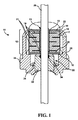
[0019]図1は、本開示の幾つかの態様によるコンデンサ構造12を含む濾波型フィードスルー組立体10の一例の断面図である。図1に示されている例では、コンデンサ構造12は、コンデンサ14と、コンデンサ14の第1表面20へ付着された第1セラミック絶縁体層16と、コンデンサ14の第2表面22へ付着された第2セラミック絶縁体層18と、を含んでいる。図1に描かれている例では、コンデンサ14は、図2−図6に描かれているモノリシック円盤状コンデンサのうちの1つの様なモノリシック円盤状コンデンサである。とはいえ、コンデンサ14がモノリシック円盤状コンデンサである例以外の他の例も考えられる。
[0019] FIG. 1 is a cross-sectional view of an example of a filtered
[0020]図1には描かれていないが、コンデンサ14は少なくとも1つのコンデンサ位置合わせ機構を含み、第1セラミック絶縁体層16は少なくとも1つのセラミック絶縁体位置合わせ機構を含み、第2セラミック絶縁体層18は少なくとも1つのセラミック絶縁体位置合わせ機構を含むものであってもよい。コンデンサ位置合わせ機構及びセラミック絶縁体位置合わせ機構の例は、図2−図6を参照しながら説明されている。更に以下に説明されている様に、その様な位置合わせ機構は、第1セラミック絶縁体層16及び/又は第2セラミック絶縁体層18をコンデンサ14の表面へ実質的に整列させるべく協働するものである。
[0020] Although not depicted in FIG. 1, capacitor 14 includes at least one capacitor alignment feature, first
[0021]図1は、コンデンサ構造12が利用されている濾波型フィードスルー組立体10の1つの例である。とはいえ、コンデンサ構造12は、他のフィードスルー組立体、例えば多極の密封シールされたフィードスルーとモノリシック円盤状コンデンサの様な多極コンデンサとを含んでいる多極フィードスルー組立体など、で使用されてもよい。コンデンサ組立体12を利用することのできる他のフィードスルー組立体の例が、2009年5月6日に「コンデンサ組立体及び関連方法」の名称で出願されている同時係属の同一出願人による米国特許出願公開第2010/0284124号に記載されている。
[0021] FIG. 1 is one example of a filtered
[0022]図1に示されている様に、濾波型フィードスルー組立体10は、導体26(端子ピン又はフィードスルーピンと称されることもある)を通して延ばす開口を画定しているフェルール24を含んでいる。フェルール24は、IMDのハウジングに形成されている開口内に取り付けることのできる材料で形成されている。幾つかの例では、フェルール24が形成されている材料は、電気伝導性材料でもある。フェルール24を作ることのできる材料の例には、チタン、ニオブ、白金、モリブデン、ジルコニウム、タンタル、バナジウム、タングステン、イリジウム、ロジウム、レニウム、オスミウム、ルテニウム、パラジウム、銀、及びそれらの合金、混合物、及び組合せ、が挙げられよう。
[0022] As shown in FIG. 1, the filtered
[0023]フェルール24によって画定されている開口内に、継手絶縁体部分組立体30が配置されている。継手絶縁体部分組立体30は、導体26をフェルール24に対して固定すると共に導体26をフェルール24から電気的に絶縁する。継手絶縁体部分組立体30は、更に、導体26とフェルール24の間に密封シールを形成している。
[0023] Within the opening defined by the
[0024]継手絶縁体部分組立体30は、図示の例では、3つの構成要素、即ち、絶縁体リング32と、金製であってもよいとされる導体絶縁体ろう付け部34と、絶縁体フェルールろう付け部36と、を含んでいる。絶縁体リング32は、電気絶縁セラミックの様な電気絶縁性材料から作ることができる。導体絶縁体ろう付け部34及び絶縁体フェルールろう付け部36は、例えば、金、白金、白金合金、又はニッケル−金合金を含んでいてもよい。幾つかの例では、導体絶縁体ろう付け部34及び絶縁体フェルールろう付け部36は同じ組成を含んでおり、また一方他の例では、導体絶縁体ろう付け部34は絶縁体フェルールろう付け部36とは異なった組成を含んでいよう。フェルール24がIMDのハウジングへ付着されたとき、フェルール24の(図1に示されている向きで)下側部分と絶縁体リング32の一部分は、体液に曝されることになる。導体絶縁体ろう付け部34は導体26と絶縁体リング32の間に密封シールを形成し、絶縁体フェルールろう付け部36は絶縁体リング32とフェルール24の間に密封シールを形成することができる。フェルール24と絶縁体リング32と導体26の間に形成される密封シールは、体液がIMDのハウジングの内部の中へ進入するのを防止することであろう。
[0024] The
[0025]導体26は、IMDのハウジング内の回路構成からIMDのハウジングの外の1つ又はそれ以上のリードワイヤへの導電経路を提供する。上述の様に、これらのリードワイヤは、IMD内の回路構成の動作に干渉しかねないEMI信号を収集するアンテナの役目を果たすものである。コンデンサ14は、導体26がコンデンサ14に形成された開口23を通るようにして導体26の周りに配置させることができる。幾つかの例では、コンデンサ14は、チタン酸バリウムの様な複数のセラミック層(図示せず)を、それら層上に形成されている導電性活性電極19及び接地電極21であって、例えばそれらの層を積重又は積層する前に層上へ電極19、21の材料である例えば銀、銀−パラジウム、又は銀−白金を印刷するなどして形成されている導電性活性電極19及び設置電極21と一体に、含んでいよう。1つの例では、活性電極19は、開口23の円周上に形成されている第1導電性被覆15へ電気的に接続している。第1導電性被覆15は、開口23の円周の少なくとも一部分に形成されていてもよく、幾つかの例では、開口23の実質的に全周囲に形成されている。幾つかの例では、第1導電性被覆15は、コンデンサ14の実質的に全長さを延びていてもよいが、他の例では、第1導電性被覆15がコンデンサ14の全長さより短く延びていることもあろう。第1導電性被覆15は、例えば、銀、銀−パラジウム、銀−白金、又は別の電気伝導性材料で形成することができる。第1導電性被覆15は導体26へ電気伝導性はんだ又はエポキシを使用して電気的に接続されていよう。
[0025]
[0026]接地電極21は、以下に更に詳細に説明されている様に、共通の大地へ、第2導電性被覆17を介するなどして、電気的に接続されている。第1導電性被覆15と同様、第2導電性被覆は、例えば、銀、銀−パラジウム、銀−白金、又は別の電気伝導性材料で形成することができる。第2導電性被覆17は、コンデンサ14の外周の少なくとも一部分に形成されていてもよく、幾つかの例では、コンデンサ14の実質的に全外周に形成されている。幾つかの例では、第2導電性被覆17は、コンデンサ14の実質的に全長さを延びていてもよいが、他の例では、第2導電性被覆17がコンデンサ14の全長さより短く延びていることもあろう。図1には示されていないが、第2導電性被覆17は、フェルール24へ、例えば、電気伝導性のはんだ、エポキシ、又はレーザー溶接の様な溶接技法を使用して、電気的に接続されていよう。
[0026] The
[0027]フェルール24が電気伝導性材料で作られている場合、導体26とIMDのハウジング(図示せず)の間には、コンデンサ14及びフェルール24を介して、導電経路が存在することであろう。コンデンサ14には、相対的に高い周波数の電気信号である例えば相対的に高い周波数のEMI信号がコンデンサ14によって濾波され、フェルール24を介してIMDのハウジングへ通される、という結果をもたらす電気特性が選択されていてもよい。コンデンサ14の電気特性は、更に、コンデンサ14が相対的に低い周波数の電気信号である例えば心臓活動又は神経活動の様な感知される生理学的パラメータを表す信号を濾波しないように選択されてもよく、そうすると、これらの相対的に低い周波数の信号はコンデンサ14によって通過させられ、導体26によってIMDのハウジング内の回路構成へ伝導される。
[0027] If the
[0028]幾つかの濾波型フィードスルー組立体10では、コンデンサ12は、第1表面20及び/又は第2表面22上に、エポキシ又は別の電気絶縁性ポリマーで形成されている電気絶縁性被覆を含んでいよう。但し、上述の様に、幾つかの例では、導体26は第1導電性被覆15へはんだを使用して電気的に接続されていてもよい。同様に、第2導電性被覆17が、追加的又は代替的に、フェルール24へはんだを使用して接続されていてもよい。鉛ベースのはんだの様な一部のはんだは、相対的に低い溶融温度を有していよう。幾つかの実施形では、鉛ベースのはんだが、鉛ベースのはんだよりも高い溶融温度を有する無鉛はんだと置き換えられている。幾つかの例では、はんだ(無鉛又は鉛ベース)は、エポキシ又は他の電気絶縁性ポリマーの軟化、溶融、又は分解の温度より上の共融点を有していることもあり、その場合、エポキシ又は他の電気絶縁性ポリマーはコンデンサ構造12での使用にあまり望ましくないであろう。
[0028] In some filtered
[0029]第1セラミック絶縁体層16及び第2セラミック絶縁体層18は、電気絶縁セラミックで形成することができる。幾つかの例では、第1セラミック絶縁体層16及び/又は第2セラミック絶縁体層18は、低温同時焼成セラミック(LTCC)又は高温同時焼成セラミック(HTCC)を含んでいる。第1セラミック絶縁体層16及び/又は第2セラミック絶縁体層18は、シート又は膜として形成され、それが所望の形状へ切断され、次いで第1表面20及び/又は第2表面へそれぞれ積層されるか又はそれ以外のやり方で付着されていてもよい。LTCCは、約1000℃未満の焼結温度を有するセラミック材料である。LTCCの1つの例は、アルミナとガラスの混合物である。幾つかの例では、ガラスは、カルシア−アルミナ−シリカ−ホウ素酸化物ガラスを含んでいよう。一例では、LTCCは、アルミナ約90重量%乃至約95重量%とガラス約5重量%乃至約10重量%の混合物を含んでいよう。HTCCは、約1000℃よりも高い焼結温度を有するセラミック材料である。HTCCの一例には、アルミナ層が挙げられよう。第1セラミック絶縁体層16及び/又は第2セラミック絶縁体層18には、他の電気絶縁性セラミックスも使用することができる。
[0029] The first
[0030]第1セラミック絶縁体層16及び第2セラミック絶縁体層18は、より高い共融温度を有するはんだの使用を(層16、18の性能に影響を及ぼすこと無く)可能にするので、鉛ベースはんだの無鉛はんだとの置き換えが促進される。上述の様に、幾つかの例では、はんだは、導体26を第1導電性被覆15へ電気的に接続するのに、及び/又は第2導電性被覆17をフェルール24へ電気的に接続するのに使用されている。幾つかの例では、第1セラミック絶縁体層16及び/又は第2セラミック絶縁体層18は、コンデンサ14の第1表面20及び第2表面22へ直接的又は間接的にそれぞれ付着されている膜として提供されている。例えば、第1セラミック絶縁体層16及び/又は第2セラミック絶縁体層18は、コンデンサ14の第1表面20及び第2表面22へ、接着剤を使用して接着されていてもよい。他の例では、第1セラミック絶縁体層16及び/又は第2セラミック絶縁体層18は、コンデンサ14の第1表面20及び第2表面22へ、熱及び/又は圧力を使用して積層されていてもよい。
[0030] Since the first
[0031]幾つかの例では、コンデンサ14の表面(例えば、第1表面20又は第2表面22)は、電気伝導性であってもよい。他の例では、第1導電性被覆15及び/又は第2導電性被覆17が、コンデンサの第1表面20及び/又は第2表面22まで延びていて、第1表面20及び/又は第2表面22に導電性材料を提供していてもよい。第1表面20及び/又は第2表面22に電気伝導性材料が在れば、導体26及び/又は第1導電性被覆15と第2導電性被覆17の間、又は(例えば図2−図6の多極フィードスルーでの)コンデンサに形成された隣り合う開口に受け入れられている隣り合う導体同士の間、のアーク放電を許してしまう。例えば、IMDへ戻る1つ又はそれ以上のリードによって導体26を介して伝導される一部の電気信号は相対的に高い電圧であるかもしれない。例えば、除細動ショックは、約780V乃至約800Vの電圧を有していることもある。第1表面20及び/又は第2表面22のアークは、より高い電圧ではより起こり易い。
[0031] In some examples, the surface of capacitor 14 (eg, first surface 20 or second surface 22) may be electrically conductive. In another example, the first
[0032]第1セラミック絶縁体層16及び/又は第2セラミック絶縁体層18は、第1表面20及び/又は第2表面22にそれぞれ電気絶縁を提供することによってアーク放電を低減するか又は実質的に防止することができる。第1セラミック絶縁体層16及び/又は第2セラミック絶縁体層18のアーク発現低減化における有効性は、第1セラミック絶縁体層16及び/又は第2セラミック絶縁体層18が第1表面20及び/又は第2表面22の導電性部分をそれぞれどれ程完全に覆っているかによって影響されることであろう。例えば、第1セラミック絶縁体層16及び/又は第2セラミック絶縁体層18は、それらが第1導電性被覆15及び第2導電性被覆17の第1表面20及び/又は第2表面22で露出してしまう部分を実質的にくまなく覆っている場合には、アーク発現低減化により有効であろう。第1セラミック絶縁体層16及び/又は第2セラミック絶縁体層18は、膜として提供されているので、絶縁性膜を、第1表面20及び/又は第2表面22の外周及び第1表面20及び/又は第2表面22に形成されている開口23の様な第1表面20及び/又は第2表面22の機構を実質的に再現するように、切断してもよいし又はそれ以外のやり方で整形してもよい。幾つかの実施形では、絶縁性膜は、第1表面20及び/又は第2表面22へ積層されるか又はそれ以外のやり方で付着される前に切断されるか又はそれ以外のやり方で整形されている。その様な実施形では、第1表面20と第1セラミック絶縁体層16の間及び/又は第2表面22と第2セラミック絶縁体層16の間の比較的精密な整列が、第1導電性被覆15及び第2導電性被覆17(又は第1表面20及び/又は第2表面22の他の導電性部分)の被覆率を向上させることであり、それによってアークを低減するか又は実質的に防止することができる。本開示の1つ又はそれ以上の例によれば、コンデンサ構造12を組み立てる際のコンデンサ14とセラミック絶縁体層16及び/又は18の整列をやり易くするために、コンデンサ位置合わせ機構とセラミック絶縁体層位置合わせ機構を採用することができる。
[0032] The first
[0033]図2は、モノリシック円盤状コンデンサ42とセラミック絶縁体層44とを含む一例としてのコンデンサ構造40の、セラミック絶縁体層44がコンデンサ42へ付着される前の斜視図である。モノリシック円盤状コンデンサ42は、図1を参照して説明されているコンデンサ14と実質的に同じか又は類似であってもよく、例えば、モノリシック円盤状コンデンサ42のセラミック層上に形成された複数の導電性活性電極19と複数の導電性接地電極21とを含んでいてもよい。モノリシック円盤状コンデンサ42は、更に、フィードスルー開口50a、50b、50c、及び50d(ひとまとめに「フィードスルー開口50」)のうちの幾つか又は全部に第1導電性被覆15と実質的に同じか又は類似の導電性被覆を含み、コンデンサ42の外周側壁43の少なくとも一部分に第2導電性被覆15と実質的に同じか又は類似の導電性被覆を含んでいてもよい。明解さを期して、図2には、第1導電性被覆15、第2導電性被覆17、導電性活性電極19、及び導電性接地電極21は示されていない。また、図2−図6は単一のセラミック絶縁体層を描いているが、幾つかの例では、コンデンサ構造は、図1のコンデンサ構造12の様な、第1セラミック絶縁体層及び第2セラミック絶縁体層を含んでいよう。コンデンサ構造が、第1及び第2のセラミック絶縁体層を含んでいる例では、一方又は両方の絶縁体層及び絶縁体層が付着している一方又は両方の表面は、ここに説明されている位置合わせ機構を含んでいよう。
FIG. 2 is a perspective view of an
[0034]モノリシック円盤状コンデンサ42は、コンデンサ外周46を画定している第1表面48を含んでいる。外周側壁43がコンデンサ外周46に沿って第1表面48に接合している。第1表面48は、モノリシック円盤状コンデンサ42を実質的に通り抜けて第1表面48とは反対側の第2表面(図示せず)まで延びている4つのフィードスルー開口50(図1に描かれている開口23に類似)を画定している。フィードスルー開口50は、導体又は端子ピン(例えば、図1の導体26)を受け入れるように構成されている。モノリシック円盤状コンデンサ42は、図1では4つのフィードスルー開口50を含んでいるが、モノリシック円盤状コンデンサ42は、少なくとも1つ、少なくとも2つ、少なくとも3つ、など、他の数のフィードスルー50を含んでいてもよい。
[0034] The monolithic disc capacitor 42 includes a
[0035]第1表面48は、更に、第1コンデンサ位置合わせ開口52a及び第2コンデンサ位置合わせ開口52b(ひとまとめに「コンデンサ位置合わせ開口54」)を画定している。コンデンサ位置合わせ開口52は、セラミック絶縁体層44のモノリシック円盤状コンデンサ42の第1表面48に対する整列をやり易くする位置合わせ機構である。コンデンサ位置合わせ開口52は、モノリシック円盤状コンデンサ42を少なくとも途中まで貫いて延びている空洞であってもよい。幾つかの例では、コンデンサ位置合わせ開口52は、モノリシック円盤状コンデンサ42を途中までしか貫いて延びておらず、一方、他の例では、コンデンサ位置合わせ開口52は、モノリシック円盤状コンデンサ42を第1表面48から第1表面48とは反対側の第2表面(図示せず)まで完全に貫いて延びている。幾つかの例では、モノリシック円盤状コンデンサ42は、1つの位置合わせ開口を含んでいることもあれば、2つより多い位置合わせ開口を含んでいることもあろう。概して、モノリシック円盤状コンデンサ42は、少なくとも1つの位置合わせ開口を含むものとすることができる。モノリシック円盤状コンデンサ42が単一の位置合わせ開口を含んでいる一部の例では、位置合わせ開口(及び対応する位置合わせピン及びセラミック絶縁体層44の位置合わせ開口)は、楕円形、矩形、方形、十字形、又は別の多角形形状の様な、非円形形状を含むものとすることができ、そうすれば、モノリシック円盤状コンデンサ42とセラミック絶縁体層44の整列は、例えばコンデンサ42と層44の直線整列と回転整列の両方が促されることによって、やり易くなるであろう。追加的又は代替的に、位置合わせ開口52は、第1表面48の図2に描かれている位置とは異なった位置に在ってもよい。
[0035] The
[0036]示されている様に、第1位置合わせピン54aが第1コンデンサ位置合わせ開口52aに挿入され、第2位置合わせピン54bが第2コンデンサ位置合わせ開口52bに挿入されていてもよい。第1位置合わせピン54aと第2位置合わせピン54b(ひとまとめに「位置合わせピン54」)は、セラミック絶縁体層44の第1表面48への積層時に、モノリシック円盤状コンデンサ42及び/又はセラミック絶縁体層44を溶融、軟化、又は融解させない材料で形成することができる。例えば、位置合わせピン54は、タンタル、ニオブ、タンタル合金、又はニオブ合金、又はアルミナの様なセラミック系材料であって、セラミック絶縁体層44が第1表面48へ積層される温度よりも高い温度で焼結する高融点金属で形成することができる。
[0036] As shown, a
[0037]コンデンサ位置合わせ開口52及び位置合わせピン54は、相補的な形状及び大きさを有するように形成されている。例えば、図2に示されている様に、コンデンサ位置合わせ開口52は円形、位置合わせピン54は円形断面を有する円筒形、とすることができる。他の例では、コンデンサ位置合わせ開口52は、楕円形、矩形、方形、又は別の多角形形状の様な、別の形状を有するものとし、位置合わせピン54は対応する断面形状を有するものとしてもよい。加えて、位置合わせピン54の大きさ(例えば、直径、円周、又は外周囲)は、位置合わせピン54の外周面がコンデンサ位置合わせ開口52の外周とぴったり係合するか又は接触するように選択されよう。位置合わせピン54とコンデンサ位置合わせ開口52の間のぴったりした嵌まり合いは、セラミック絶縁体層44の第1表面48に対する整列をやり易くする。位置合わせピン54は、セラミック絶縁体層44が第1表面48と接触に置かれたときに、セラミック絶縁体層44を貫通して延びるのに十分な長さとすることができる。
[0037] The capacitor alignment opening 52 and alignment pin 54 are formed to have complementary shapes and sizes. For example, as shown in FIG. 2, the capacitor alignment opening 52 may be circular and the alignment pin 54 may be cylindrical with a circular cross section. In other examples, the capacitor alignment aperture 52 may have another shape, such as an oval, rectangular, square, or another polygon shape, and the alignment pin 54 may have a corresponding cross-sectional shape. Also good. In addition, the size (eg, diameter, circumference, or outer perimeter) of the alignment pin 54 is such that the outer peripheral surface of the alignment pin 54 closely engages or contacts the outer periphery of the capacitor alignment opening 52. Will be selected. The close fit between the alignment pin 54 and the capacitor alignment opening 52 facilitates alignment of the ceramic insulator layer 44 with respect to the
[0038]セラミック絶縁体層44は、外周45と、4つのフィードスルー開口56a、56b、56c、及び56d(ひとまとめに「フィードスルー開口56」)と、を画定している。加えて、セラミック絶縁体層44は、第1セラミック絶縁体位置合わせ開口58a及び第2セラミック絶縁体位置合わせ開口58b(ひとまとめに「位置合わせ開口58」を画定している。フィードスルー開口56及び位置合わせ開口58の数、大きさ、及び位置は、単に例であり、セラミック絶縁体層44の他の例は、異なった数、大きさ、及び/又は位置のフィードスルー開口56及び位置合わせ開口58を含んでいることもあろう。概して、セラミック絶縁体層44は、モノリシック円盤状コンデンサ42に形成されているフィードスルー開口50の数と同じ数のフィードスルー開口56を含むものとすることができる。
[0038] The ceramic insulator layer 44 defines an
[0039]位置合わせ開口58とフィードスルー開口56と外周45の相対位置は、位置合わせ開口58をコンデンサ位置合わせ開口52に整列させたときに、フィードスルー開口56がフィードスルー開口50と実質的に整列し、外周45が外周46と実質的に整列するような相対位置である。このやり方では、位置合わせ開口58とコンデンサ位置合わせ開口52と位置合わせピン54は協働してセラミック絶縁体層44をモノリシック円盤状コンデンサ42の第1表面48に実質的に整列させる。
[0039] The relative positions of the alignment opening 58, the feedthrough opening 56, and the
[0040]セラミック絶縁体層44の位置合わせ開口58は、大きさ及び形状が、コンデンサ位置合わせ開口52と実質的に同様である。例えば、位置合わせ開口58は、円形、楕円形、矩形、方形、又は別の多角形形状とすることができる。コンデンサ位置合わせ開口52に関連付けて説明されている様に、位置合わせピン56と位置合わせ開口58の間のぴったりした嵌まり合いがセラミック絶縁体層44の第1表面48に対する整列をやり易くする。
[0040] The alignment opening 58 of the ceramic insulator layer 44 is substantially similar in size and shape to the capacitor alignment opening 52. For example, the alignment aperture 58 can be circular, elliptical, rectangular, square, or another polygonal shape. As described in connection with the capacitor alignment opening 52, the close fit between the alignment pin 56 and the alignment opening 58 facilitates alignment of the ceramic insulator layer 44 with respect to the
[0041]コンデンサ構造40を組み立てるに当たり、モノリシック円盤状コンデンサ42には、コンデンサ42の初期製造時か又は以降の機械加工工程時の何れかの時期に、フィードスルー開口50及び位置合わせ開口52が形成されることになる。フィードスルー開口50及び位置合わせ開口52を形成するのに、穿孔、レーザー切断、水ジェット切断、など、の様な各種技法が使用できよう。幾つかの例では、フィードスルー開口50のうち少なくとも幾つかの開口の少なくとも一部分に第1導電性被覆15が形成され、外周側壁43の少なくとも一部分に第2導電性被覆17が形成されよう。
[0041] In assembling the
[0042]セラミック絶縁体層44は、LTCC膜又はHTCC膜の様なセラミック絶縁体膜から形成することができる。幾つかの例では、セラミック絶縁体層44は、例えばレーザー切断を使用して、膜から切り出されてもよい。セラミック絶縁体層44の形成時、フィードスルー開口56及び位置合わせ開口58が、例えばセラミック絶縁体層44を切り出すのに使用されているのと同じプロセスを使用して、セラミック絶縁体層44に形成されてもよい。切断プロセスは、コンピュータ数値制御(CNC)機械の様なコンピュータによって制御させれば、外周45、フィードスルー開口56、及び位置合わせ開口58の精密な相対的位置付けがやり易くなるであろう。
[0042] The ceramic insulator layer 44 may be formed from a ceramic insulator film, such as an LTCC film or an HTCC film. In some examples, the ceramic insulator layer 44 may be cut from the film using, for example, laser cutting. During formation of the ceramic insulator layer 44, feedthrough openings 56 and alignment openings 58 are formed in the ceramic insulator layer 44, for example using the same process used to cut out the ceramic insulator layer 44. May be. If the cutting process is controlled by a computer such as a computer numerical control (CNC) machine, precise relative positioning of the
[0043]次いで、位置合わせピン54がコンデンサ位置合わせ開口52に設置されると、位置合わせ開口58を位置合わせピン54と整列させた状態でセラミック絶縁体層44が第1表面48上に位置付けられる。位置合わせ開口58と位置合わせピン54と位置合わせ開口52は協働してセラミック絶縁体層44とモノリシック円盤状コンデンサ42の第1表面48を実質的に整列させる。例えば、フィードスルー開口56及び外周45を含むセラミック絶縁体層44は、フィードスルー開口50及び外周46を含むモノリシック円盤状コンデンサ42の第1表面48に実質的に整列させられる。
[0043] Next, when the alignment pin 54 is installed in the capacitor alignment opening 52, the ceramic insulator layer 44 is positioned on the
[0044]位置合わせされたら、セラミック絶縁体層44は第1表面48へ付着されてもよい。幾つかの実施形では、セラミック絶縁体層44は、ポリイミド材料やガラス材料などの様な接着剤を使用して、第1表面48へ接着されてもよい。他の例では、セラミック絶縁体層44は、温度及び圧力を使用して、第1表面48へ積層されてもよい。例えば、セラミック絶縁体層44がLTCCを含んでいる場合、層44は、約800℃乃至約900℃の温度及び約800ポンド/平方インチ(psi)乃至約1500psiの圧力で、第1表面48へ積層させることができる。セラミック絶縁体層44が第1表面48へ積層された後、位置合わせピン54は抜かれてもよい。
[0044] Once aligned, the ceramic insulator layer 44 may be applied to the
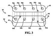
[0045]図3は、モノリシック円盤状コンデンサ62とセラミック絶縁体層44とを含む一例としてのコンデンサ構造60の、セラミック絶縁体層44がコンデンサ62へ付着される前の斜視図である。図2に関連付けて説明されている様に、セラミック絶縁体層44は、外周45、フィードスルー開口56、及び位置合わせ開口58を画定している。
FIG. 3 is a perspective view of an
[0046]モノリシック円盤状コンデンサ62は、図2に関連付けて説明されている様に外周側壁43に接合する外周46を画定している第1表面48を含んでいる。加えて、第1表面48は4つのフィードスルー開口50を画定している。図1のモノリシック円盤状コンデンサ42に関連付けて説明されている第1表面48によって画定される位置合わせ開口52を含む代わりに、モノリシック円盤状コンデンサ62は、第1表面48上に形成されている第1位置合わせ突起64a及び第2位置合わせ突起64b(ひとまとめに「位置合わせ突起64」)を含んでいる。位置合わせ突起64は、第1表面48とセラミック絶縁体層44の整列をやり易くするコンデンサ位置合わせ機構である。幾つかの例では、モノリシック円盤状コンデンサ62は、1つの位置合わせ突起を含んでいることもあれば、2つより多い位置合わせ突起を含んでいることもあろう。概して、モノリシック円盤状コンデンサ62は、少なくとも1つの位置合わせ突起を含むものとすることができる。以上に図2に関連付けて説明されている様に、幾つかの例では、単一の位置合わせ突起は、楕円形、方形、矩形、十字形、又は他の多角形の様な、非円形形状を含むものとすることができる。追加的又は代替的に、位置合わせ突起62は、第1表面48の図3に描かれている位置とは異なった位置に在ってもよい。
[0046] The
[0047]幾つかの例では、位置合わせ突起64は、モノリシック円盤状コンデンサ62が形成される材料の1つで形成されている。例えば、位置合わせ突起64は、チタン酸バリウムの様な、モノリシック円盤状コンデンサ62に使用されている電気絶縁セラミック材料で形成されていてもよい。幾つかの例では、位置合わせ突起64は、モノリシック円盤状コンデンサ62の製造時に形成されよう。他の例では、位置合わせ突起64は、モノリシック円盤状コンデンサ62の製造とは切り離して、例えば、セラミック絶縁体層44を第1表面48へ付着させる前に、形成されてもよい。
[0047] In some examples, the alignment protrusion 64 is formed of one of the materials from which the
[0048]位置合わせ突起64及び位置合わせ開口58は、相補的な形状及び大きさを有するように形成されている。例えば、図3に示されている様に、位置合わせ突起64は円形断面を有する円筒形、位置合わせ開口58は円形、とすることができる。他の例では、位置合わせ突起64は、楕円形、矩形、方形、又は別の多角形形状の様な、別の断面形状を有するものとし、位置合わせ開口58は対応する形状を有するものとしてもよい。加えて、位置合わせ突起64の大きさ(例えば、直径、円周、又は外周囲)は、位置合わせ開口58の外周面が位置合わせ突起64の外周とぴったり係合するか又は接触するように選択されよう。位置合わせ突起64と位置合わせ開口58の間のぴったりした嵌まり合いは、セラミック絶縁体層44の第1表面48に対する整列をやり易くする。位置合わせ突起64は、セラミック絶縁体層44が第1表面48と接触に置かれたときに、セラミック絶縁体層44を貫通して延びるのに十分な長さとすることができる。
[0048] The alignment protrusion 64 and the alignment opening 58 are formed to have complementary shapes and sizes. For example, as shown in FIG. 3, the alignment protrusion 64 may be cylindrical with a circular cross section, and the alignment opening 58 may be circular. In other examples, the alignment protrusion 64 may have another cross-sectional shape, such as an oval, rectangular, square, or another polygonal shape, and the alignment opening 58 may have a corresponding shape. Good. In addition, the size (eg, diameter, circumference, or outer perimeter) of the alignment protrusion 64 is selected such that the outer peripheral surface of the alignment opening 58 closely engages or contacts the outer periphery of the alignment protrusion 64. Let's do it. The close fit between the alignment protrusion 64 and the alignment opening 58 facilitates alignment of the ceramic insulator layer 44 with respect to the
[0049]位置合わせ開口58とフィードスルー開口56と外周45の相対位置は、位置合わせ開口58を位置合わせ突起64と合わせたときに、フィードスルー開口56がフィードスルー開口50と実質的に整列し、外周45が外周46と実質的に整列するような相対位置である。このやり方では、位置合わせ開口58と位置合わせ突起64は協働してセラミック絶縁体層44をモノリシック円盤状コンデンサ62の第1表面48に実質的に整列させる。
[0049] The relative positions of the alignment opening 58, the feedthrough opening 56 and the
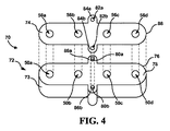
[0050]図4は、モノリシック円盤状コンデンサ72とセラミック絶縁体層74とを含む一例としてのコンデンサ構造70の、セラミック絶縁体層74がコンデンサ72へ付着される前の斜視図である。
FIG. 4 is a perspective view of an
[0051]モノリシック円盤状コンデンサ72は、4つのフィードスルー開口50を画定している第1表面78を含んでいる。上述の様に、他の例では、第1表面78は、別の数のフィードスルー開口50を画定していることもあり、概して、少なくとも1つのフィードスルーを画定するものとすることができる。加えて、第1表面78は、外周側壁73に接合する外周76を画定している。図2及び図3では、モノリシック円盤状コンデンサ42、62は、実質的に円盤状(例えば、長円形又は楕円形)の外周を画定していた。図4に示されている例では、モノリシック円盤状コンデンサ72は、コンデンサ72の円盤状の形状を中断させている第1突出部86a及び第2突出部86b(ひとまとめに「突出部86」)を含む外周76を画定している。突出部86は、外周側壁73の一部であり、第1表面78から第1表面78とは反対側の第2表面(図示せず)まで延びている。
[0051] The monolithic disc capacitor 72 includes a
[0052]第1表面78の突出部86の部分である部分には、第1位置合わせ突起80a及び第2位置合わせ突起80b(ひとまとめに「位置合わせ突起80」)が形成されている。位置合わせ突起80は、図3を参照して説明されている位置合わせ突起64に類似している。位置合わせ突起80は、第1表面78とセラミック絶縁体層74の整列をやり易くするコンデンサ位置合わせ機構である。
[0052] A first alignment protrusion 80a and a
[0053]図4は、2つの突出部86と2つの位置合わせ突起80を含んでいるモノリシック円盤状コンデンサ72を描いているが、他の例では、モノリシック円盤状コンデンサ72は、2つより多い突出部86及び/又は2つより多い位置合わせ突起80を含んでいてもよい。幾つかの例では、突出部86の各1つに位置合わせ突起80が形成されて含まれている。追加的又は代替的に、1つ又はそれ以上の位置合わせ突起80は、第1表面78の一方の突出部86の部分ではない部分に形成されていてもよい。
[0053] FIG. 4 depicts a monolithic disc capacitor 72 that includes two protrusions 86 and two alignment protrusions 80, but in other examples, there are more than two monolithic disc capacitors 72. The protrusion 86 and / or more than two alignment protrusions 80 may be included. In some examples, an alignment protrusion 80 is formed and included in each one of the protrusions 86. Additionally or alternatively, one or more alignment protrusions 80 may be formed on a portion of the
[0054]幾つかの例では、突出部86及び/又は位置合わせ突起80は、モノリシック円盤状コンデンサ72が形成される材料の1つで形成されている。例えば、突出部86及び/又は位置合わせ突起80は、チタン酸バリウムの様な、モノリシック円盤状コンデンサ72に使用されている電気絶縁セラミック材料で形成されていてもよい。幾つかの例では、突出部86及び/又は位置合わせ突起80は、モノリシック円盤状コンデンサ72の製造時に形成されよう。他の例では、突出部86及び/又は位置合わせ突起80は、モノリシック円盤状コンデンサ72の製造とは切り離して、例えば、セラミック絶縁体層74を第1表面78へ付着させる前に、形成されてもよい。
[0054] In some examples, the protrusions 86 and / or alignment protrusions 80 are formed of one of the materials from which the monolithic disc capacitor 72 is formed. For example, the protrusion 86 and / or the alignment protrusion 80 may be formed of an electrically insulating ceramic material used in the monolithic disc capacitor 72, such as barium titanate. In some examples, the protrusions 86 and / or alignment protrusions 80 may be formed during manufacture of the monolithic disc capacitor 72. In other examples, the protrusions 86 and / or alignment protrusions 80 may be formed separately from the manufacture of the monolithic disc capacitor 72, for example, prior to attaching the
[0055]セラミック絶縁体層74は、外周88及び4つのフィードスルー開口56を画定している。セラミック絶縁体層74は、モノリシック円盤状コンデンサ72の突出部86と実質的に大きさが一致していてそれと整列している第1突出部84a及び第2突出部84b(ひとまとめに「突出部84」)を含んでいる。セラミック絶縁体層74は、第1突出部84aに第1セラミック絶縁体位置合わせ開口82aを、そして第2突出部84bに第2セラミック絶縁体位置合わせ開口82bを、画定している。概して、セラミック絶縁体層74は、モノリシック円盤状コンデンサ72に形成されているフィードスルー開口50、突出部86、及び位置合わせ突起80の数及び配置と同じ数及び配置のフィードスルー開口56、突出部84、及びコンデンサ位置合わせ開口82を含むものとすることができる。図3の位置合わせ突起64及び位置合わせ開口58と同様に、位置合わせ突起80及び位置合わせ開口82は、相補的な形状及び大きさを有するように形成されている。突出部84と位置合わせ開口82とフィードスルー開口56と外周88の相対位置は、位置合わせ開口82を位置合わせ突起80に整列させたときに、フィードスルー開口56がフィードスルー開口50と実質的に整列し、外周88が外周76と実質的に整列するような相対位置である。このやり方では、位置合わせ開口82と位置合わせ突起80は協働してセラミック絶縁体層74をモノリシック円盤状コンデンサ72の第1表面78に実質的に整列させる。
[0055] The
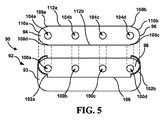
[0056]図5は、モノリシック円盤状コンデンサ92とセラミック絶縁体層94とを含む一例としてのコンデンサ構造90の、セラミック絶縁体層94がコンデンサ92へ付着される前の斜視図である。図5に描かれている例では、コンデンサ位置合わせ機構は、モノリシック円盤状コンデンサ92の外周106の少なくとも一部分に沿ってモノリシック円盤状コンデンサ92の第1表面98から実質的に垂直に延びている第1位置合わせ突起102a及び第2位置合わせ突起102b(ひとまとめに「位置合わせ突起102」)を含んでいる。セラミック絶縁体位置合わせ機構は、セラミック絶縁体層94の外周96を含んでいる。
FIG. 5 is a perspective view of an
[0057]モノリシック円盤状コンデンサ92は、4つのフィードスルー開口100a、100b、100c、100d(ひとまとめに「フィードスルー開口100」)を画定している第1表面98を含んでいる。上述の様に、他の例では、第1表面98は、別の数のフィードスルー開口100を画定していることもあり、概して、少なくとも1つのフィードスルー開口を画定するものとすることができる。加えて、第1表面98は、外周側壁93に接合する外周106を画定している。外周側壁93は、第1表面98から第1表面98とは実質的に反対側の第2表面(図示せず)まで延びている。図5に示されている例では、モノリシック円盤状コンデンサ92は、第1表面98から実質的に垂直(直角)に延びる位置合わせ突起102を画定している。図5では、位置合わせ突起102は、第1表面98の外周106の湾曲部分に沿って走っている。他の例では、モノリシック円盤状コンデンサ92は、2つより多い位置合わせ突起102を含んでいてもよいし、位置合わせ突起102の少なくとも1つは外周106に沿った異なった位置に在ってもよい。幾つかの例では、モノリシック円盤状コンデンサ92は、外周106の少なくとも一部分に沿って形成されている単一突起を含んでいよう。幾つかの実施形では、単一突起は、外周106の実質的に全長さに沿って形成されていてもよい。概して、モノリシック円盤状コンデンサ92は、外周106に沿って形成されている少なくとも1つの突出を含むものとすることができる。位置合わせ突起102は、第1表面98から測定して少なくともセラミック絶縁体層94の厚さと同じ程の高さを有するものとすることができる。
[0057] The
[0058]セラミック絶縁体層94は、外周96、第1フィードスルー開口104a、第2フィードスルー開口104b、第3フィードスルー開口104c、及び第4フィードスル開口104d(ひとまとめに「フィードスルー開口104」)を画定している。概して、セラミック絶縁体層94は、モノリシック円盤状コンデンサ92に形成されているフィードスルー開口100の数及び配置と同じ数及び配置のフィードスルー開口104を含んでいる。
[0058] The
[0059]セラミック絶縁体層94の外周96は、セラミック絶縁体層94が第1表面98を実質的に覆い、外周96が位置合わせ突起102と実質的に整列するように形成され、そういう大きさである。例えば、図5に描かれている様に、外周96は、第1段状部分108a、第2段状部分108b、第3段状部分108c、第4段状部分108d(ひとまとめに「段状部分108」)を含んでいる。外周96は、更に、第1曲線部分110a及び第2曲線部分110b(ひとまとめに「曲線部分110」)と、第1直線部分112a及び第2直線部分112b(ひとまとめに「直線部分112」)と、を含んでいる。第1段状部分108aは第1曲線部分110aと第1直線部分112aに接続している。第2段状部分108bは第1直線部分112aと第2曲線線部分110bに接続している。第3段状部分108cは第2曲線部分110bと第2直線部分112bに接続している。第4段状部分108cは第2直線部分112bと第1曲線部分110aに接続している。
[0059] The
[0060]段状部分108、曲線部分110、及び直線部分112は、セラミック絶縁体層94が第1表面98の実質的に全部を覆い、段状部分108と曲線部分110が位置合わせ突起102に接触してセラミック絶縁体94と第1表面98を実質的に整列させるような大きさ及び形状である。例えば、段状部分108及び曲線部分110は、モノリシック円盤状コンデンサ92のフィードスルー開口100とセラミック絶縁体層104のフィードスルー開口104を実質的に整列させるように位置合わせ突起102に接触するものとすることができる。このやり方では、外周96と位置合わせ突起102は協働してセラミック絶縁体層94をモノリシック円盤状コンデンサ92の第1表面98に実質的に整列させる。
[0060] In the stepped portion 108, the curved portion 110, and the straight portion 112, the
[0061]図2−図5に示されている例は、フィードスルー開口及び外周が、セラミック絶縁体層をモノリシック円盤状コンデンサと整列させる前に画定されているセラミック絶縁体層を描いているが、幾つかの例では、セラミック絶縁体層とモノリシック円盤状コンデンサは、セラミック絶縁体層に外周及び/又はフィードスルー開口を形成する前に整列させてもよい。図6は、モノリシック円盤状コンデンサ122とセラミック絶縁体層124とを含む一例としてのコンデンサ構造120の、セラミック絶縁体層124がコンデンサ122へ付着される前で且つセラミック絶縁体層124に外周及びフィードスルー開口が画定される前の斜視図である。
[0061] The example shown in FIGS. 2-5 depicts a ceramic insulator layer in which the feedthrough opening and perimeter are defined before aligning the ceramic insulator layer with the monolithic disc capacitor. In some examples, the ceramic insulator layer and the monolithic disc capacitor may be aligned prior to forming the perimeter and / or feedthrough opening in the ceramic insulator layer. FIG. 6 illustrates an
[0062]図6に描かれている例では、モノリシック円盤状コンデンサ122は、外周側壁123に接合する外周126を画定している第1表面128を含んでいる。加えて、第1表面128は、4つのフィードスルー開口130a、130b、130c、130d(ひとまとめに「フィードスルー開口130」)を画定している。モノリシック円盤状コンデンサ122は、第1表面128上に形成されている第1位置合わせ突起132a及び第2位置合わせ突起132b(ひとまとめに「位置合わせ突起132」)を含んでいる。位置合わせ突起132は、図3に関連付けて説明されている位置合わせ突起64及び/又は図4に関連付けて説明されている位置合わせ突起80と同じか又は実質的に類似であってもよい。
In the example depicted in FIG. 6, the
[0063]セラミック絶縁体層124は、第1位置合わせ開口134a及び第2位置合わせ開口134b(ひとまとめに「位置合わせ開口134」)を画定している膜を含んでいる。位置合わせ突起132と位置合わせ開口134は、上述の様に、相補的な数、形状、及び大きさを有するように形成されている。
[0063] The
[0064]位置合わせ開口134を位置合わせ突起132と整列させた後、セラミック絶縁体層124は第1表面128と接触に置かれる。位置合わせ開口134と位置合わせ突起132は協働してセラミック絶縁体層124をモノリシック円盤状コンデンサ122の第1表面128に実質的に整列させる。ひとたび第1表面128と接触したら、セラミック絶縁体層124は上述の様に第1表面128へ接着されるか又は積層されることになる。セラミック絶縁体層124を第1表面128へ積層した後、セラミック絶縁体層124のモノリシック円盤状コンデンサ122のフィードスルー開口130に実質的に対応する位置にフィードスルー開口が切られることになる。加えて、セラミック絶縁体層124は、モノリシック円盤状コンデンサ122の外周126に実質的に対応する外周を画定するように切断されることになる。幾つかの例では、セラミック絶縁体層124は、レーザー切断を使用して切断されてもよい。
[0064] After aligning the alignment opening 134 with the alignment protrusion 132, the
[0065]代わりに、セラミック絶縁体層124は、層124を第1表面128と接触に置いた後で第1表面128へ接着又は積層する前に切断されてもよい。ひとたびセラミック絶縁体層214の外周及びセラミック絶縁体層124のフィードスルー開口が切られたら、セラミック絶縁体層124は第1表面128へ接着、積層、又はそれ以外のやり方で付着させることができる。
[0065] Alternatively, the
[0066]図2−図6は、主に、セラミック絶縁体層に形成されている位置合わせ開口とコンデンサから延びている位置合わせピン又は位置合わせ突起を説明しているが、他の例では、位置合わせ陥凹又は開口がコンデンサの表面に形成され、位置合わせ突起がセラミック絶縁体層側に形成されていてもよい。幾つかの例では、セラミック絶縁体層が位置合わせ開口と位置合わせ突起を両方含み、コンデンサが対応する位置合わせ突起と位置合わせ陥凹又は開口を含むようにすることもできる。追加的又は代替的に、図2−図6は別々の例として説明されているが、それぞれの図に記載されている位置合わせ機構が互いと組み合わせて使用されてもよい。例えば、コンデンサは、コンデンサの外周に沿ってコンデンサの表面から延びている突起(図6)を含み、且つコンデンサの外周から離れて形成されている突起(図3)を含んでいてもよい。 [0066] FIGS. 2-6 primarily illustrate alignment openings formed in the ceramic insulator layer and alignment pins or alignment protrusions extending from the capacitor, but in other examples, An alignment recess or opening may be formed on the surface of the capacitor, and an alignment protrusion may be formed on the ceramic insulator layer side. In some examples, the ceramic insulator layer may include both alignment openings and alignment protrusions, and the capacitor may include corresponding alignment protrusions and alignment recesses or openings. Additionally or alternatively, FIGS. 2-6 are described as separate examples, but the alignment mechanisms described in each figure may be used in combination with each other. For example, the capacitor may include protrusions (FIG. 6) that extend from the surface of the capacitor along the outer periphery of the capacitor, and protrusions (FIG. 3) that are formed away from the outer periphery of the capacitor.
[0067]図7は、本開示の幾つかの例によるコンデンサ構造を形成するのに使用することのできる一例としての技法を示している流れ図である。図7の一例としての技法は、主に、コンデンサ構造40(図2)に関連付けて説明されているが、但し、本技法は、図3のコンデンサ構造60、図4のコンデンサ構造70、図5のコンデンサ構造90、図6のコンデンサ構造120、又は他のコンデンサ構造に適用可能であろう。概して、本技法は、少なくとも1つのセラミック絶縁体層位置合わせ機構を少なくとも1つのコンデンサ位置合わせ機構(例えば、コンデンサ位置合わせ開口52及び位置合わせピン54)と整列させる段階(144)を含むものである。上述の様に、少なくとも1つのセラミック絶縁体層位置合わせ機構には、位置合わせ開口(例えば、位置合わせ開口58、82、134)、セラミック絶縁体層の外周(例えば、外周96)、及び/又はセラミック絶縁体層の外周に形成されている機構(例えば、段状部分108及び曲線部分110)が含まれよう。少なくとも1つのコンデンサ位置合わせ機構には、例えば、コンデンサ位置合わせ開口52及び位置合わせピン54又は位置合わせ突起64、80、102、132が含まれよう。コンデンサ位置合わせ機構とセラミック絶縁体層位置合わせ機構は協働してセラミック絶縁体層をモノリシック円盤状コンデンサの表面に実質的に整列させる。
[0067] FIG. 7 is a flow diagram illustrating an example technique that may be used to form a capacitor structure according to some examples of this disclosure. The exemplary technique of FIG. 7 has been described primarily in connection with capacitor structure 40 (FIG. 2), except that the technique includes
[0068]ひとたび少なくとも1つのセラミック絶縁体層位置合わせ機構を少なくとも1つのコンデンサ位置合わせ機構と整列させたら(144)、セラミック絶縁体層44をモノリシック円盤状コンデンサ42の第1表面48と接触に置き、第1表面48へ付着させる(146)。上述の様に、セラミック絶縁体層44は、第1表面48へ接着又は積層させてもよい。例えば、セラミック絶縁体層44がLTCCを含んでいる場合、層44は約800℃乃至約900℃の温度及び約800ポンドpsi乃至約1500psiの圧力で、第1表面48へ積層させることができる。
[0068] Once the at least one ceramic insulator layer alignment feature is aligned with the at least one capacitor alignment feature (144), the ceramic insulator layer 44 is placed in contact with the
[0069]幾つかの例では、セラミック絶縁体層42のフィードスルー開口56及び外周45は、セラミック絶縁体層44をモノリシック円盤状コンデンサ42へ積層する段階(146)の前に形成されてもよい。他の例では、セラミック絶縁体層42のフィードスルー開口56及び外周45は、上述の様に、セラミック絶縁体層44をモノリシック円盤状コンデンサ42へ積層する段階(146)の後に形成されてもよい。
[0069] In some examples, the feedthrough opening 56 and
[0070]LTCC組成を含んでいるセラミック絶縁体をモノリシック円盤状コンデンサの表面へ積層してコンデンサ構造を形成した。LTCC組成は、アルミナ約90重量%乃至約95重量%とガラス(CaO−Al2O3−SiO2−B2O3)約5重量%乃至約10重量%を含有。LTCC組成を、約800℃乃至約900℃の温度及び約800psi乃至約1500psiの圧力で、コンデンサへ積層した。 [0070] A ceramic insulator containing the LTCC composition was laminated to the surface of a monolithic disc capacitor to form a capacitor structure. The LTCC composition contains about 90 wt.% To about 95 wt.% Alumina and about 5 wt.% To about 10 wt.% Glass (CaO—Al 2 O 3 —SiO 2 —B 2 O 3 ). The LTCC composition was laminated to the capacitor at a temperature of about 800 ° C. to about 900 ° C. and a pressure of about 800 psi to about 1500 psi.
[0071]次いで、コンデンサ構造をフィードスルー組立体に組み立てた。コンデンサ構造を、フィードスルー開口の中のフィードスルーピンへ、そしてコンデンサ外周に沿ってフィードスルーフェルールへ、はんだを使用して接続した。コンデンサを、フェルールへの電気接続を介して大地へ接続した。 [0071] The capacitor structure was then assembled into a feedthrough assembly. The capacitor structure was connected using solder to the feedthrough pin in the feedthrough opening and to the feedthrough ferrule along the periphery of the capacitor. A capacitor was connected to ground through an electrical connection to the ferrule.
[0072]フィードスルー組立体に、−55℃から125℃の間で5サイクルの熱ショック試験を課し、約125℃でフィードスルーピンとフェルールの間に1000Vのバイアス電圧を印加してバーンインした。 [0072] The feedthrough assembly was subjected to a five-cycle heat shock test between -55 ° C and 125 ° C and burned in at about 125 ° C with a bias voltage of 1000 V applied between the feedthrough pin and the ferrule.
[0073]バーンイン調整の後、フィードスルー組立体を電気的に試験した。フィードスルー組立体に、フィードスルーピンと大地の間に1300V、隣り合うフィードスルーピン同士の間に1000Vを使って、パルス試験を課した。パルスの立ち上がり時間は約1乃至2マイクロ秒で、パルスの一時停止時間は約18ミリ秒であった。 [0073] After burn-in conditioning, the feedthrough assembly was electrically tested. The feedthrough assembly was subjected to a pulse test using 1300 V between the feedthrough pin and ground and 1000 V between adjacent feedthrough pins. The pulse rise time was about 1-2 microseconds and the pulse pause time was about 18 milliseconds.
[0074]フィードスルー組立体には、更に、誘電耐電圧試験を課した。フィードスルーピンと大地の間に1300Vの電圧を印加し、隣り合うフィードスルーピン同士の間に1000Vを印加した。電圧のそれぞれは、ピーク電圧で約5秒保持された。 [0074] The feedthrough assembly was further subjected to a dielectric withstand voltage test. A voltage of 1300 V was applied between the feedthrough pin and the ground, and 1000 V was applied between adjacent feedthrough pins. Each of the voltages was held at the peak voltage for about 5 seconds.
[0075]最後に、フィードスルー組立体に絶縁抵抗試験を課した。フィードスルーピンと大地の間に1300Vの電圧を印加し、隣り合うフィードスルーピン同士の間に1000Vを印加した。抵抗を測定したところ、30ギガオームより大きかった。フィードスルー組立体及びコンデンサ構造は以上の試験全てに何の不具合もなく合格した。 [0075] Finally, an insulation resistance test was imposed on the feedthrough assembly. A voltage of 1300 V was applied between the feedthrough pin and the ground, and 1000 V was applied between adjacent feedthrough pins. When the resistance was measured, it was greater than 30 gigaohms. The feedthrough assembly and capacitor structure passed all of the above tests without any failure.
10 濾波型フィードスルー組立体
12 コンデンサ構造
14 コンデンサ
15 第1導電性被覆
16 第1セラミック絶縁体層
17 第2導電性被覆
18 第2セラミック絶縁体層
19 導電性活性電極
20 コンデンサの第1表面
21 導電性接地電極
22 コンデンサの第2表面
23 コンデンサの開口
24 フェルール
26 導体
30 継手絶縁体部分組立体
32 絶縁体リング
34 導体絶縁体ろう付け部
36 絶縁体フェルールろう付け部
40 コンデンサ構造
42 モノリシック円盤状コンデンサ
43 コンデンサの外周側壁
44 セラミック絶縁体層
45 セラミック絶縁体層の外周
46 コンデンサの外周
48 コンデンサの第1表面
50、50a、50b、50c、50d フィードスルー開口
52、52a、52b コンデンサ位置合わせ開口
54、54a、54b 位置合わせピン
56、56a、56b、56c、56d フィードスルー開口
58、58a、58b セラミック絶縁体位置合わせ開口
60 コンデンサ構造
62 モノリシック円盤状コンデンサ
64、64a、64b 位置合わせ突起
70 コンデンサ構造
72 モノリシック円盤状コンデンサ
73 コンデンサの外周側壁
74 セラミック絶縁体層
76 コンデンサの外周
78 コンデンサの第1表面
80、80a、80b 位置合わせ突起
82、82a、82b 位置合わせ開口
84、84a、84b セラミック絶縁体層の突出部
86、86a、86b コンデンサの突出部
88 セラミック絶縁体層の外周
90 コンデンサ構造
92 モノリシック円盤状コンデンサ
93 コンデンサの外周側壁
94 セラミック絶縁体層
96 セラミック絶縁体層の外周
98 コンデンサの第1表面
100、100a、100b、100c、100d フィードスルー開口
102、102a、102b 位置合わせ突起
104、104a、104b、104c、104d フィードスルー開口
106 コンデンサの外周
108、108a、108b、108c、108d 段状部分
110、110a、110b 曲線部分
112、112a、112b 直線部分
120 コンデンサ構造
122 モノリシック円盤状コンデンサ
123 コンデンサの側壁
124 セラミック絶縁体層
126 コンデンサの外周
128 コンデンサの第1表面
130、130a、130b、130c、130d フィードスルー開口
132、132a、32b 位置合わせ突起
134、134a、134b 位置合わせ開口
DESCRIPTION OF SYMBOLS 10 Filter type feedthrough assembly 12 Capacitor structure 14 Capacitor 15 First conductive coating 16 First ceramic insulator layer 17 Second conductive coating 18 Second ceramic insulator layer 19 Conductive active electrode 20 First surface 21 of capacitor 21 Conductive ground electrode 22 Capacitor second surface 23 Capacitor opening 24 Ferrule 26 Conductor 30 Joint insulator subassembly 32 Insulator ring 34 Conductor insulator brazed portion 36 Insulator ferrule brazed portion 40 Capacitor structure 42 Monolithic disk shape Capacitor 43 Peripheral side wall of capacitor 44 Ceramic insulator layer 45 Perimeter of ceramic insulator layer 46 Perimeter of capacitor 48 First surface of capacitor 50, 50a, 50b, 50c, 50d Feedthrough opening 52, 52a, 52b Capacitor alignment Openings 54, 54a, 54b Alignment pins 56, 56a, 56b, 56c, 56d Feedthrough openings 58, 58a, 58b Ceramic insulator alignment openings 60 Capacitor structure 62 Monolithic disc capacitors 64, 64a, 64b Alignment protrusions 70 Capacitors Structure 72 Monolithic disc capacitor 73 Peripheral side wall of capacitor 74 Ceramic insulator layer 76 Perimeter of capacitor 78 First surface of capacitor 80, 80a, 80b Alignment protrusion 82, 82a, 82b Alignment opening 84, 84a, 84b Ceramic insulator Protrusion of layer 86, 86a, 86b Protrusion of capacitor 88 Perimeter of ceramic insulator layer 90 Capacitor structure 92 Monolithic disc capacitor 93 Peripheral side wall of capacitor 94 Ceramic insulation Body layer 96 Perimeter of ceramic insulator layer 98 First surface of capacitor 100, 100a, 100b, 100c, 100d Feedthrough opening 102, 102a, 102b Alignment protrusion 104, 104a, 104b, 104c, 104d Feedthrough opening 106 of capacitor Peripheral part 108, 108a, 108b, 108c, 108d Stepped part 110, 110a, 110b Curved part 112, 112a, 112b Straight part 120 Capacitor structure 122 Monolithic disk capacitor 123 Capacitor sidewall 124 Ceramic insulator layer 126 Capacitor outer periphery 128 Capacitor First surface 130, 130a, 130b, 130c, 130d Feedthrough opening 132, 132a, 32b Alignment protrusion 134, 134a, 134 Alignment openings
Claims (3)
少なくとも1つのフィードスルー開口を画定している表面を備えるコンデンサであって、前記表面はコンデンサ位置合わせ機構を備えている、コンデンサと、
前記表面へ付着されているセラミック絶縁体層であって、当該セラミック絶縁体層は、少なくとも1つのフィードスルー開口を画定していてセラミック絶縁体層位置合わせ機構を含んでおり、前記コンデンサ位置合わせ機構と当該セラミック絶縁体層位置合わせ機構が協働して、前記セラミック絶縁体層を前記コンデンサに実質的に整列させるとともに、前記セラミック絶縁体層に画定されている前記少なくとも1つのフィードスルー開口を前記コンデンサの前記表面に画定されている少なくとも1つのフィードスルー開口と実質的に整列させる、セラミック絶縁体層とを備えており、
前記コンデンサ位置合わせ機構は、位置合わせ開口、又は、前記表面から実質的に垂直に延びる位置合わせ突起を備えており、
前記表面は外周を備えており、前記突起は前記外周の一部分に沿って延びている、コンデンサ構造。 In the capacitor structure,
A capacitor comprising a surface defining at least one feedthrough opening, the surface comprising a capacitor alignment mechanism;
A ceramic insulator layer attached to the surface, the ceramic insulator layer defining at least one feedthrough opening and including a ceramic insulator layer alignment mechanism; and the capacitor alignment mechanism And the ceramic insulator layer alignment mechanism cooperate to substantially align the ceramic insulator layer with the capacitor and to define the at least one feedthrough opening defined in the ceramic insulator layer. A ceramic insulator layer substantially aligned with at least one feedthrough opening defined in the surface of the capacitor;
The capacitor alignment mechanism includes an alignment opening or alignment protrusion extending substantially perpendicularly from the surface;
The capacitor structure , wherein the surface has an outer periphery, and the protrusion extends along a portion of the outer periphery .
フェルール開口を画定しているフェルールと、
導体と、
請求項1又は2に記載のコンデンサ構造とを備えているフィードスルー組立体。 In the feedthrough assembly,
A ferrule defining a ferrule opening; and
Conductors,
A feedthrough assembly comprising the capacitor structure according to claim 1.
Applications Claiming Priority (3)
| Application Number | Priority Date | Filing Date | Title |
|---|---|---|---|
| US13/149,600 | 2011-05-31 | ||
| US13/149,600 US8644002B2 (en) | 2011-05-31 | 2011-05-31 | Capacitor including registration feature for aligning an insulator layer |
| PCT/US2012/039826 WO2012166709A2 (en) | 2011-05-31 | 2012-05-29 | Capacitor including registration feature for aligning an insulator layer |
Publications (3)
| Publication Number | Publication Date |
|---|---|
| JP2014520393A JP2014520393A (en) | 2014-08-21 |
| JP2014520393A5 JP2014520393A5 (en) | 2015-04-02 |
| JP6010612B2 true JP6010612B2 (en) | 2016-10-19 |
Family
ID=46229936
Family Applications (1)
| Application Number | Title | Priority Date | Filing Date |
|---|---|---|---|
| JP2014513638A Active JP6010612B2 (en) | 2011-05-31 | 2012-05-29 | Capacitor including alignment mechanism for aligning insulator layers |
Country Status (4)
| Country | Link |
|---|---|
| US (2) | US8644002B2 (en) |
| EP (1) | EP2715752B1 (en) |
| JP (1) | JP6010612B2 (en) |
| WO (1) | WO2012166709A2 (en) |
Families Citing this family (9)
| Publication number | Priority date | Publication date | Assignee | Title |
|---|---|---|---|---|
| US10441802B2 (en) | 2013-08-28 | 2019-10-15 | Heartware, Inc. | Pass-through assembly |
| US9387331B2 (en) | 2013-10-08 | 2016-07-12 | Medtronic, Inc. | Implantable medical devices having hollow cap cofire ceramic structures and methods of fabricating the same |
| US9138821B2 (en) * | 2014-01-17 | 2015-09-22 | Medtronic, Inc. | Methods for simultaneously brazing a ferrule and lead pins |
| US10363425B2 (en) | 2015-06-01 | 2019-07-30 | Avx Corporation | Discrete cofired feedthrough filter for medical implanted devices |
| KR101656723B1 (en) * | 2015-06-30 | 2016-09-12 | 재단법인 오송첨단의료산업진흥재단 | Feedthrough making method |
| DE102016107414A1 (en) | 2016-04-21 | 2017-10-26 | Biotronik Se & Co. Kg | Implementation of an implantable medical electronic device and implantable medical electronic device |
| US10741223B2 (en) | 2016-06-06 | 2020-08-11 | Western Digital Technologies, Inc. | Sealed bulkhead electrical feed-through positioning control |
| US10350422B2 (en) * | 2017-06-09 | 2019-07-16 | Medtronic, Inc. | Feedthrough assembly including ferrule with tapered extension(s) |
| US11224754B2 (en) * | 2019-05-23 | 2022-01-18 | Medtronic, Inc. | Feedthrough assembly with feature for controlling component position |
Family Cites Families (56)
| Publication number | Priority date | Publication date | Assignee | Title |
|---|---|---|---|---|
| US3920888A (en) | 1974-06-04 | 1975-11-18 | Nuclear Battery Corp | Electrical feed-through assembly suitable for electronic devices implantable in a human body |
| US4152540A (en) | 1977-05-03 | 1979-05-01 | American Pacemaker Corporation | Feedthrough connector for implantable cardiac pacer |
| US4421947A (en) | 1977-10-11 | 1983-12-20 | James C. Kyle | Polycrystalline insulating material seals between spaced members such as a terminal pin and a ferrule |
| JPS5745955A (en) | 1980-09-02 | 1982-03-16 | Seikosha Co Ltd | Sealing container |
| US4424551B1 (en) | 1982-01-25 | 1991-06-11 | Highly-reliable feed through/filter capacitor and method for making same | |
| JPH01312819A (en) * | 1988-06-09 | 1989-12-18 | Tdk Corp | Manufacture of feedthrough-type capacitor |
| US4991582A (en) | 1989-09-22 | 1991-02-12 | Alfred E. Mann Foundation For Scientific Research | Hermetically sealed ceramic and metal package for electronic devices implantable in living bodies |
| JPH0793230B2 (en) * | 1991-03-22 | 1995-10-09 | 太陽誘電株式会社 | How to stack ceramic sheets |
| US5287076A (en) | 1991-05-29 | 1994-02-15 | Amphenol Corporation | Discoidal array for filter connectors |
| JP2868376B2 (en) * | 1992-09-07 | 1999-03-10 | 日本カーバイド工業株式会社 | LC substrate and manufacturing method thereof |
| JPH06244057A (en) * | 1992-12-26 | 1994-09-02 | Murata Mfg Co Ltd | Element assembly for feedthrough capacitor |
| US5406444A (en) * | 1993-03-29 | 1995-04-11 | Medtronic, Inc. | Coated tantalum feedthrough pin |
| US5333095A (en) | 1993-05-03 | 1994-07-26 | Maxwell Laboratories, Inc., Sierra Capacitor Filter Division | Feedthrough filter capacitor assembly for human implant |
| US5434358A (en) | 1993-12-13 | 1995-07-18 | E-Systems, Inc. | High density hermetic electrical feedthroughs |
| US5470345A (en) | 1994-06-16 | 1995-11-28 | Medtronic, Inc. | Implantable medical device with multi-layered ceramic enclosure |
| US5782891A (en) | 1994-06-16 | 1998-07-21 | Medtronic, Inc. | Implantable ceramic enclosure for pacing, neurological, and other medical applications in the human body |
| US5735884A (en) | 1994-10-04 | 1998-04-07 | Medtronic, Inc. | Filtered feedthrough assembly for implantable medical device |
| AU3299995A (en) | 1994-10-04 | 1996-04-18 | Medtronic, Inc. | Protective feedthrough |
| US5685632A (en) | 1995-05-31 | 1997-11-11 | Rayovac Corporation | Electrically conductive plastic light source |
| US5817984A (en) | 1995-07-28 | 1998-10-06 | Medtronic Inc | Implantable medical device wtih multi-pin feedthrough |
| US5750926A (en) | 1995-08-16 | 1998-05-12 | Alfred E. Mann Foundation For Scientific Research | Hermetically sealed electrical feedthrough for use with implantable electronic devices |
| US5650759A (en) | 1995-11-09 | 1997-07-22 | Hittman Materials & Medical Components, Inc. | Filtered feedthrough assembly having a mounted chip capacitor for medical implantable devices and method of manufacture therefor |
| US5620476A (en) | 1995-11-13 | 1997-04-15 | Pacesetter, Inc. | Implantable medical device having shielded and filtered feedthrough assembly and methods for making such assembly |
| US5751539A (en) | 1996-04-30 | 1998-05-12 | Maxwell Laboratories, Inc. | EMI filter for human implantable heart defibrillators and pacemakers |
| US5825608A (en) | 1996-10-18 | 1998-10-20 | Novacap, Inc. | Feed-through filter capacitor assembly |
| US5870272A (en) | 1997-05-06 | 1999-02-09 | Medtronic Inc. | Capacitive filter feedthrough for implantable medical device |
| US5896267A (en) | 1997-07-10 | 1999-04-20 | Greatbatch-Hittman, Inc. | Substrate mounted filter for feedthrough devices |
| US5905627A (en) | 1997-09-10 | 1999-05-18 | Maxwell Energy Products, Inc. | Internally grounded feedthrough filter capacitor |
| US6275369B1 (en) | 1997-11-13 | 2001-08-14 | Robert A. Stevenson | EMI filter feedthough terminal assembly having a capture flange to facilitate automated assembly |
| US6008980A (en) | 1997-11-13 | 1999-12-28 | Maxwell Energy Products, Inc. | Hermetically sealed EMI feedthrough filter capacitor for human implant and other applications |
| US5959829A (en) | 1998-02-18 | 1999-09-28 | Maxwell Energy Products, Inc. | Chip capacitor electromagnetic interference filter |
| US5973906A (en) | 1998-03-17 | 1999-10-26 | Maxwell Energy Products, Inc. | Chip capacitors and chip capacitor electromagnetic interference filters |
| US5999398A (en) | 1998-06-24 | 1999-12-07 | Avx Corporation | Feed-through filter assembly having varistor and capacitor structure |
| JP2000260661A (en) * | 1999-03-08 | 2000-09-22 | Nec Niigata Ltd | Chip component and chip component mounting board |
| US6414835B1 (en) | 2000-03-01 | 2002-07-02 | Medtronic, Inc. | Capacitive filtered feedthrough array for an implantable medical device |
| US6529103B1 (en) * | 2000-09-07 | 2003-03-04 | Greatbatch-Sierra, Inc. | Internally grounded feedthrough filter capacitor with improved ground plane design for human implant and other applications |
| US6456481B1 (en) * | 2001-05-31 | 2002-09-24 | Greatbatch-Sierra, Inc. | Integrated EMI filter-DC blocking capacitor |
| US7038900B2 (en) * | 2003-02-27 | 2006-05-02 | Greatbatch-Sierra, Inc. | EMI filter terminal assembly with wire bond pads for human implant applications |
| US6898066B1 (en) * | 2004-06-21 | 2005-05-24 | Chieh-Fu Lin | Structure of chip type electrolytic capacitor |
| US7196899B1 (en) * | 2005-01-07 | 2007-03-27 | Pacesetter, Inc. | Capacitor anode assembly |
| US7068491B1 (en) | 2005-09-15 | 2006-06-27 | Medtronic, Inc. | Implantable co-fired electrical interconnect systems and devices and methods of fabrication therefor |
| US20070060970A1 (en) | 2005-09-15 | 2007-03-15 | Burdon Jeremy W | Miniaturized co-fired electrical interconnects for implantable medical devices |
| US20070203529A1 (en) | 2006-02-28 | 2007-08-30 | Iyer Rajesh V | Filtered feedthrough assembly |
| US7668597B2 (en) | 2006-03-31 | 2010-02-23 | Medtronic, Inc. | Feedthrough array for use in implantable medical devices |
| US9042999B2 (en) | 2006-06-08 | 2015-05-26 | Greatbatch Ltd. | Low loss band pass filter for RF distance telemetry pin antennas of active implantable medical devices |
| EP1977786B1 (en) | 2007-04-03 | 2012-11-28 | Biotronik CRM Patent AG | A filtering assembly and a feedthrough assembly |
| US8059386B2 (en) | 2007-09-25 | 2011-11-15 | Medtronic, Inc. | Capacitive elements and filtered feedthrough elements for implantable medical devices |
| US7928818B2 (en) | 2007-09-25 | 2011-04-19 | Medtronic, Inc. | Capacitive elements and filtered feedthrough elements for implantable medical devices |
| US20090079517A1 (en) | 2007-09-25 | 2009-03-26 | Iyer Rajesh V | Novel capacitive elements and filtered feedthrough elements for implantable medical devices |
| EP2269200B1 (en) | 2008-03-20 | 2014-09-24 | Greatbatch Ltd. | Shielded three-terminal flat-through emi/energy dissipating filter |
| US8391983B2 (en) | 2008-05-08 | 2013-03-05 | Pacesetter, Inc. | Implantable pulse generator EMI filtered feedthru |
| US8373965B2 (en) | 2009-02-10 | 2013-02-12 | Medtronic, Inc. | Filtered feedthrough assembly and associated method |
| US9009935B2 (en) | 2009-05-06 | 2015-04-21 | Medtronic, Inc. | Methods to prevent high voltage arcing under capacitors used in filtered feedthroughs |
| US8725263B2 (en) | 2009-07-31 | 2014-05-13 | Medtronic, Inc. | Co-fired electrical feedthroughs for implantable medical devices having a shielded RF conductive path and impedance matching |
| US20110048770A1 (en) | 2009-08-31 | 2011-03-03 | Medtronic Inc. | Injection molded ferrule for cofired feedthroughs |
| US8373075B2 (en) | 2009-10-29 | 2013-02-12 | Medtronic, Inc. | Implantable co-fired electrical feedthroughs |
-
2011
- 2011-05-31 US US13/149,600 patent/US8644002B2/en active Active
-
2012
- 2012-05-29 JP JP2014513638A patent/JP6010612B2/en active Active
- 2012-05-29 WO PCT/US2012/039826 patent/WO2012166709A2/en active Application Filing
- 2012-05-29 EP EP12726537.9A patent/EP2715752B1/en active Active
-
2013
- 2013-12-23 US US14/138,197 patent/US20140111904A1/en not_active Abandoned
Also Published As
| Publication number | Publication date |
|---|---|
| EP2715752A2 (en) | 2014-04-09 |
| WO2012166709A2 (en) | 2012-12-06 |
| CN103563025A (en) | 2014-02-05 |
| US8644002B2 (en) | 2014-02-04 |
| JP2014520393A (en) | 2014-08-21 |
| EP2715752B1 (en) | 2017-10-25 |
| US20140111904A1 (en) | 2014-04-24 |
| WO2012166709A3 (en) | 2013-01-24 |
| US20120307416A1 (en) | 2012-12-06 |
Similar Documents
| Publication | Publication Date | Title |
|---|---|---|
| JP6010612B2 (en) | Capacitor including alignment mechanism for aligning insulator layers | |
| EP2750760B1 (en) | Feedthrough assembly including a capacitive filter array | |
| USRE48348E1 (en) | Feedthrough filter capacitor assembly with internally grounded hermetic insulator | |
| US9931514B2 (en) | Low impedance oxide resistant grounded capacitor for an AIMD | |
| EP1488434B1 (en) | Emi feedthrough filter terminal assembly utilizing hermetic seal for electrical attachment between lead wires and capacitor | |
| US9427596B2 (en) | Low impedance oxide resistant grounded capacitor for an AIMD | |
| EP2207594B1 (en) | Novel capacitive elements and filtered feedthrough elements for implantable medical devices | |
| JP6336610B2 (en) | Filtered feedthrough assembly for implantable medical devices and method of manufacturing the same | |
| EP2429654B1 (en) | Capacitor assembly and associated method | |
| US8644936B2 (en) | Feedthrough assembly including electrical ground through feedthrough substrate | |
| US20070239223A1 (en) | Feedthrough array for use in implantable medical devices | |
| US20130138186A1 (en) | Feedthrough assembly including capacitor array on printed board | |
| US8331077B2 (en) | Capacitor for filtered feedthrough with annular member | |
| US20130138187A1 (en) | Feedthrough assembly including chip capacitors | |
| US20210162220A1 (en) | Electrical Connection For A Hermetic Terminal For An Active Implantable Medical Device Utilizing A Ferrule Pocket | |
| CN103563025B (en) | Capacitor including the registration features for being directed at insulator layer |
Legal Events
| Date | Code | Title | Description |
|---|---|---|---|
| A521 | Request for written amendment filed |
Free format text: JAPANESE INTERMEDIATE CODE: A523 Effective date: 20150206 |
|
| A621 | Written request for application examination |
Free format text: JAPANESE INTERMEDIATE CODE: A621 Effective date: 20150206 |
|
| A977 | Report on retrieval |
Free format text: JAPANESE INTERMEDIATE CODE: A971007 Effective date: 20151116 |
|
| A131 | Notification of reasons for refusal |
Free format text: JAPANESE INTERMEDIATE CODE: A131 Effective date: 20151217 |
|
| A601 | Written request for extension of time |
Free format text: JAPANESE INTERMEDIATE CODE: A601 Effective date: 20160316 |
|
| A601 | Written request for extension of time |
Free format text: JAPANESE INTERMEDIATE CODE: A601 Effective date: 20160414 |
|
| A601 | Written request for extension of time |
Free format text: JAPANESE INTERMEDIATE CODE: A601 Effective date: 20160517 |
|
| A521 | Request for written amendment filed |
Free format text: JAPANESE INTERMEDIATE CODE: A523 Effective date: 20160613 |
|
| TRDD | Decision of grant or rejection written | ||
| A01 | Written decision to grant a patent or to grant a registration (utility model) |
Free format text: JAPANESE INTERMEDIATE CODE: A01 Effective date: 20160819 |
|
| A61 | First payment of annual fees (during grant procedure) |
Free format text: JAPANESE INTERMEDIATE CODE: A61 Effective date: 20160916 |
|
| R150 | Certificate of patent or registration of utility model |
Ref document number: 6010612 Country of ref document: JP Free format text: JAPANESE INTERMEDIATE CODE: R150 |
|
| R250 | Receipt of annual fees |
Free format text: JAPANESE INTERMEDIATE CODE: R250 |
|
| R250 | Receipt of annual fees |
Free format text: JAPANESE INTERMEDIATE CODE: R250 |
|
| R250 | Receipt of annual fees |
Free format text: JAPANESE INTERMEDIATE CODE: R250 |
|
| R250 | Receipt of annual fees |
Free format text: JAPANESE INTERMEDIATE CODE: R250 |
|
| R250 | Receipt of annual fees |
Free format text: JAPANESE INTERMEDIATE CODE: R250 |