JP6002934B2 - Discharge unit and air purifier using the same - Google Patents
Discharge unit and air purifier using the same Download PDFInfo
- Publication number
- JP6002934B2 JP6002934B2 JP2012213655A JP2012213655A JP6002934B2 JP 6002934 B2 JP6002934 B2 JP 6002934B2 JP 2012213655 A JP2012213655 A JP 2012213655A JP 2012213655 A JP2012213655 A JP 2012213655A JP 6002934 B2 JP6002934 B2 JP 6002934B2
- Authority
- JP
- Japan
- Prior art keywords
- discharge
- electrode
- discharge unit
- counter electrode
- air
- Prior art date
- Legal status (The legal status is an assumption and is not a legal conclusion. Google has not performed a legal analysis and makes no representation as to the accuracy of the status listed.)
- Active
Links
Images


Description
本発明は、室内空間の除菌や脱臭を行う、コロナ放電を利用した空気清浄装置に関するものである。 The present invention relates to an air cleaning device that uses corona discharge to sterilize and deodorize indoor spaces.
従来、コロナ放電を利用して、オゾンやマイナスイオンなどを発生させる装置が知られている。その構成は、針電極と、アース電極とを有し、前記針電極とアース電極間に高電圧を印加して、針電極先端部においてコロナ放電を生起させ、このコロナ放電により、オゾンおよびマイナスイオンを発生させるものであった(例えば特許文献1参照)。 2. Description of the Related Art Conventionally, devices that generate ozone, negative ions, etc. using corona discharge are known. The configuration includes a needle electrode and a ground electrode, and a high voltage is applied between the needle electrode and the ground electrode to cause a corona discharge at the tip of the needle electrode. By this corona discharge, ozone and negative ions are generated. (For example, refer to Patent Document 1).
上記従来の特許文献1に記載の装置では、放電のスパークを防止するために、放電電極としての針電極と対向電極としてのアース電極の距離を離す必要があった。また、針電極とアース電極を平行に配置しているため、イオン風の発生方向と、コロナ放電の発生部位がずれ、生成したオゾンなどの活性種を効率的に拡散させることができず、活性種の放出量を増やすことは困難であった。 In the conventional device described in Patent Document 1, it is necessary to increase the distance between the needle electrode as the discharge electrode and the ground electrode as the counter electrode in order to prevent the spark of the discharge. In addition, since the needle electrode and the earth electrode are arranged in parallel, the direction of ionic wind generation and the site of corona discharge are shifted, and the generated active species such as ozone cannot be efficiently diffused. It was difficult to increase the amount of seed release.
そこで、本発明は、放電のスパークを防止しつつ放電電極と対向電極の距離を近づけ、イオンの放出量を増やすことができる放電ユニットおよびこれを用いた空気清浄装置を提供することを目的とする。 SUMMARY OF THE INVENTION Accordingly, an object of the present invention is to provide a discharge unit and an air cleaning device using the discharge unit that can increase the discharge amount of ions by reducing the distance between the discharge electrode and the counter electrode while preventing spark of discharge. .
そして、この目的を達成するために本発明は、放電電極と対向電極に電源部から電圧を印加してコロナ放電させる放電ユニットにおいて、前記放電電極は針状電極であり、前記対向電極は平板状で、この平板状の対向電極に対して前記針状の放電電極を非接触で、直交に、かつ、その先端を突出させて配置し、前記放電電極の先端が突出した側の、前記対向電極の表面が、半導電性を有する構成とし、これにより所期の目的を達成するものである。 In order to achieve this object, the present invention provides a discharge unit in which a voltage is applied from a power supply unit to a discharge electrode and a counter electrode to perform corona discharge. The discharge electrode is a needle electrode, and the counter electrode is a flat plate. The needle-like discharge electrode is arranged in a non-contact manner, orthogonal to the flat plate-like counter electrode, with its tip protruding, and the counter electrode on the side where the tip of the discharge electrode protrudes. The surface has a semiconductivity, thereby achieving the intended purpose.
以上のように本発明は、放電電極と対向電極に電源部から電圧を印加してコロナ放電させる放電ユニットにおいて、前記放電電極は針状電極であり、前記対向電極は平板状で、この平板状の対向電極に対して前記針状の放電電極を非接触で、直交に、かつ、その先端を突出させて配置し、前記放電電極の先端が突出した側の、前記対向電極の表面が、半導電性を有する構成としたものであるので、放電のスパークを防止しつつ放電電極と対向電極の距離を近づけ、イオンの放出量を増やすことができる。 As described above, the present invention relates to a discharge unit in which a voltage is applied to a discharge electrode and a counter electrode from a power supply unit to perform corona discharge. The discharge electrode is a needle-like electrode, the counter electrode has a flat plate shape, and the flat plate shape. The needle-like discharge electrode is arranged in a non-contact, orthogonal, and projecting tip with respect to the counter electrode, and the surface of the counter electrode on the side where the tip of the discharge electrode projects is half Since the structure has conductivity, it is possible to increase the amount of ions released by reducing the distance between the discharge electrode and the counter electrode while preventing discharge sparks.
すなわち、本発明においては、対向電極の放電電極の先端突出側表面が半導電性を有する構成としたことにより、対向電極と放電電極の距離を近くでき、その結果放電電流が増えるため、イオンの発生量を増やすことができる。 That is, in the present invention, since the tip protruding side surface of the discharge electrode of the counter electrode has a semiconductive configuration, the distance between the counter electrode and the discharge electrode can be reduced, and as a result, the discharge current increases. The amount of generation can be increased.
また、放電電極が対向電極に対して非接触で直交して、かつ、その先端を突出させているため、コロナ放電により発生するイオン風の風量を増加させ、例えば放電電極に+電圧を印加した場合、発生したプラスイオンがアースに接続された対向電極に電気的に吸引されるのを抑制でき、イオン風を効率的に利用して、発生したイオンを放出できる。 In addition, since the discharge electrode is non-contacting and orthogonal to the counter electrode, and its tip protrudes, the amount of ion wind generated by corona discharge is increased, for example, a positive voltage is applied to the discharge electrode. In this case, the generated positive ions can be prevented from being electrically attracted to the counter electrode connected to the ground, and the generated ions can be released by efficiently using the ion wind.
また、複数の放電ユニットを備えて、各々の放電電極と対向電極に同一電源部から電圧を印加してコロナ放電させる放電ユニットにおいて、少なくとも一つの前記放電ユニットの前記放電電極と前記対向電極の位置関係は、前記対向電極が、前記放電電極の先端側近傍で、前記放電電極の略垂直方向に対向配置させたことより、オゾンなどの活性種の発生量を増やすことができる。 In the discharge unit comprising a plurality of discharge units and applying corona discharge by applying a voltage from the same power source to each discharge electrode and the counter electrode, the positions of the discharge electrode and the counter electrode of at least one of the discharge units The relationship is that the amount of generation of active species such as ozone can be increased because the counter electrode is arranged in the vicinity of the tip end side of the discharge electrode in the substantially vertical direction of the discharge electrode.
(実施の形態1)
以下、本発明の実施の形態について、図面を参照しながら説明する。
(Embodiment 1)
Hereinafter, embodiments of the present invention will be described with reference to the drawings.
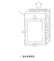
図1に示すように、空気清浄装置1は、略縦長箱形状で、前面の四方から室内の空気を吸込み、後述するエアフィルタ2で清浄し、本発明の放電ユニットで発生させたイオンと静電霧化ユニットで発生させた活性種を清浄空気とともに天面から室内へ送風するものである。
As shown in FIG. 1, the air purifier 1 has a substantially vertically long box shape, sucks indoor air from the front four sides, cleans it with an
図2は、図1における空気清浄装置1の断面図を示している。 FIG. 2 shows a cross-sectional view of the air cleaning device 1 in FIG.
空気清浄装置1は、吸気口3と排気口4を有する本体5と、この本体5内の送風手段6と、放電ユニット7および静電霧化ユニット8とを備えている。
The air cleaning device 1 includes a
本体5は、吸気口3の反対側に位置する仕切板部9によって、吸気口3と排気口4とを連通する風路部10と、空間部11とに分けられている。
The
送風手段6は、本体5の仕切板部9に固定された電動機12と、この電動機12によって回転する羽根部13とから形成している。送風手段6によって、吸気口3から吸い込んだ空気の一部は、放電ユニット7および静電霧化ユニット8を介して、排気口4へ送風されるものである。
The air blowing means 6 is formed of an
放電ユニット7は、図3〜図4に示すように絶縁性基板16と、絶縁性基板16の放電電極17先端側の表面に設けた半導電部18と、この半導電部18の外周縁に設けた導電部23とからなる対向電極14と、絶縁性基板16の円形の孔部21を貫通して配置された放電電極17と、支持部材22と、導電部23と電気的に接続された電源接続部19と、この電源接続部19および放電電極17に電圧を印加する電源部20(図2に記載)とから形成している。
As shown in FIGS. 3 to 4, the
なお、孔部21を設けなくても、例えば絶縁性基板16が半分の大きさで半円の切欠を有する形状でも、イオン量を増やすことは可能である。従来の特許文献に記載のように、針電極とアース電極を平行に配置した場合、コロナ放電領域は、針電極とからアース電極側に偏って生成するため、放電領域が小さくなる。一方、本発明のように、放電電極と半導電部を略垂直方向に対向配置した場合、針からみて円錐状に広がりを持ったコロナ放電領域が形成されるため、コロナ放電領域の範囲が広がり、より多くの活性種を発生させることができる。孔部21を設けた場合には、孔部21の端面に向かってコロナ放電が発生するため、孔部21の直径を変えることによってコロナ放電の広がり方を変化させることができる。
Even if the
絶縁性基板16は、図3、図4に示すごとく、平板形状で略中央に開口である孔部21を有し、絶縁性基板16の端部は、支持部材22を介して本体ケースの仕切板部9に固定されている。
As shown in FIGS. 3 and 4, the
支持部材22は、対向電極14を両面から挟み込むように固定する固定蓋22aと台座22b、および放電電極17を固定する底板22cで構成され、図3に示す分解した部材を組立てると、図4のような全側面の一部を開口した筒形状となる構成であり、支持部材22が内部に放電電極17と対向電極14を設けたケースを構成している。
The
放電ユニット7は、上述のごとく絶縁性基板16と、この絶縁性基板16の孔部21を貫通して配置された放電電極17と、絶縁性基板16の孔部21の内面と絶縁性基板16の放電電極17側の表面とに設けた半導電部18と、この半導電部18の外周部を覆うごとく電気的に接続されるように設けた導電部23と、この導電部23と電気的に接続された電源接続部19と、電源部20を設けたものである。
As described above, the
電源接続部19は、SUSなどのステンレス、アルミ、金、銀、銅などで形成されている。なお、これらに限られること無く、導電性の素材であれば良い。
The
放電ユニット7は、対向電極14と、放電電極17と、対向電極14と放電電極17を保持する支持部材22とを備えている。支持部材22は、仕切板部9(図2に記載)に固定されている。
The
以下で、各構成の特徴を図3、図4を用いて詳細に説明する。 Hereinafter, the characteristics of each component will be described in detail with reference to FIGS.
対向電極14を構成する絶縁性基板16は、四角平板形状であり、略中央に開口する孔部21を有している。なお、絶縁性基板の形状は円形や多角形であってもよく、孔部の形状としても、円形状ではなく、四角形・多角形・楕円形状としてもよい。
The
さらに絶縁性基板16は、オゾンやラジカルで腐食されにくい無機系のもの、あるいは、フッ素樹脂であれば良く、セラミック基板であっても、フッ素などの樹脂基板であっても良い。セラミック基板としては、Si、Al、Zn、Ti、Mgを含む酸化物あるいは複合酸化物、炭化物、窒化物などを用いることができ、コストと入手のしやすさからアルミナが好適である。なお、絶縁性基板16の表面抵抗は、1010Ω/□以上であることが望ましい。
Furthermore, the
また半導電部18は、図3に示すように、絶縁性基板16の一方面側の表面、つまり、放電電極17の先端が突出した面と、絶縁性基板16の孔部21の内面とに設けられている。放電電極17の先端側から見ると、半導電部18の形状はリング形状である。半導電部18の表面抵抗は、106から1010Ω/□であることが望ましい。ここで、表面抵抗率は、1000V印加時の値である。
Further, as shown in FIG. 3, the
さらに半導電部18は、絶縁性基板16の表面にスクリーン印刷によりスキージで半導電インクを塗布したものである。半導電インクは、酸化スズなどの導電剤とガラス粉などの接着剤を含み、前記成分を溶剤に混合あるいは溶解させたものである。
Further, the
接着剤は、導電剤粒子と、絶縁性基板16とを接着できればよい。接着剤としてガラス粉やコロイダルシリカ、シリケート化合物、チタネート化合物などを用いてもよい。ガラス粉は化学的に不活性で耐酸化性があり、好ましい。アルミナやジルコニア、チタニアの粉末あるいはフッ素樹脂粒子などを用いてもよい。接着剤の大きさは、形状を安定化させるために導電材粒子よりも大きいほうが好ましく、導電材の2〜100倍程度の大きさにすると良い。
The adhesive only needs to adhere the conductive agent particles and the insulating
導電剤粒子としては、酸化スズが酸化に対する安定性と入手の容易さの理由で好ましく、他にはZnO、PbO2,CdO,In2O3、Tl2O3、Ga2O3、Fe3O4などの酸化物導電材およびこれらの複合酸化物などが使用可能である。導電剤としての酸化スズ(SnO2)にSbなどをドープしたものを用いてもよい。
The conductive agent particles, preferably at ease reasons of availability and tin oxide are stable against oxidation, Other ZnO, PbO 2, CdO, In 2
半導電部18として、導電剤としてのSnO2と、接着剤としてのガラスを用いる場合の構成割合は、1:4〜1:1、すなわち導電剤が20〜50%、ガラスが80〜50%が好ましく、強度面から接着剤としてのガラスは50%以上必要で、半導電性、すなわち表面抵抗率を106〜1010Ω/□とするためには、導電剤を20%以上いれることが望ましい。
The composition ratio in the case of using SnO 2 as a conductive agent and glass as an adhesive as the
接着剤としてガラスを用いる場合には、ガラス粉末を適度な溶媒を加えて混合し、作成した半導電性インキを絶縁性基板16に印刷し、ガラスが溶融する温度まで加熱して、ガラス中に導電剤が分散した状態を作る方法などが挙げられる。また、酸化スズとガラスと接着剤を混合して作成したインキに、絶縁性の基板をディップして乾燥させる方法などが挙げられる。
When glass is used as an adhesive, glass powder is mixed with an appropriate solvent, and the prepared semiconductive ink is printed on the insulating
また導電部23は、図3に示すように、半導電部18の周縁部近傍の表面外周部を覆う位置に設けられており、この導電部23は電源接続部19と半導電部18と電気的に接続しているものである。このとき、放電電極17から導電部23までの最短距離は、放電電極17から半導電部18までの最短距離よりも長いものである。図3の例では、導電部23は、四角形状の金属性平板であり、孔部21の外周よりも大きい貫通孔24を有する。
Further, as shown in FIG. 3, the
このような構成とすることにより、放電電極17と電極端子19間を流れる電流は、例えば放電電極17から絶縁性基板16の孔部21の内面を覆う半導電部18を流れた後に、絶縁性基板16の一方面表面を覆う半導電部18を流れ、その後、導電部23を介して、ようやく電源接続部19へと到達することになる。つまり、沿面距離が長いので、その結果として火花放電が起こらず、安全性の向上が図れるものである。
With this configuration, the current flowing between the
ここで、導電部23の表面抵抗率は、半導電部18の表面抵抗率より小さいものである。具体的には、半導電部18の表面抵抗率は、106Ω/□以上から1010Ω/□未満であり、導電部23の表面抵抗率は、106Ω/□未満であり、電源接続部19の表面抵抗率は、10-1Ω/□以下であることが望ましい。
Here, the surface resistivity of the
さらに導電部23は、孔部21の中心から略等距離に位置するものである。具体的には、半導電部18の孔部21の外周から外方へ略等距離延びた位置で電気的に接続するリング形状であり、この周縁部に導電部23が位置するものである。つまり、放電電極17の先端から略等距離に導電部23が位置するものである。
Furthermore, the
これにより、導電部23は、孔部21の外周から略等距離に位置するので、放電電極17と電源接続部19間に高電圧が印加された場合に、放電電極17と電源接続部19間を流れる電流は、導電部23全周に均一に流れ易くなる。また、半導電部18の周縁部まで流れた電流は、導電部23の表面抵抗率が、半導電部18の表面抵抗率より小さいものであるので、導電部23を介して電源接続部19へ到達し易くなる。
As a result, since the
すなわち、半導電部18の広い範囲に電流が均一に分散し、更に、半導電部18の周縁部に位置する導電部23へ広がるように電流が流れるので、半導電部18の狭い範囲に電流が集中し、集中的に活性種を生成することなく、さらに局所的に発熱することがないため、半導電部18の劣化を抑制することができるものである。
That is, the current is uniformly distributed over a wide range of the
導電部23は、金属製平板であることが望ましい。導電部23をAg、Cu、カーボンなどを含む導電性インクによる印刷で形成することもできるが、長期間使用する際には導電インクの劣化が課題となる。金属製平板であれば、インクに比べて、放電によって生成した活性種に対する酸化安定性が優れているため、結果として活性種を安定して発生させることができる。
The
導電部23の材質は、SUS316L、SUS316、SUS304、アルマイト処理を施したアルミニウムのいずれかからなるものであることが望ましい。これらの金属は、オゾン等の活性種に対する耐性が高いため、オゾン等の活性種による腐食に強く、導電部23の耐久性を向上できるからである。なお、導電部23は、これらに限られること無く、導電性の素材であれば良い。導電部23の表面抵抗は、10-1Ω/□以下であることが望ましい。
The material of the
さらに導電部23の外形を支持部材22の内部と略同一の四角形状とすれば、放電ユニット7の組立工程において、導電部23の位置決めを容易にすることができる。
Further, if the outer shape of the
また、電源接続部19は、絶縁性基板16における放電電極17の先端が突出した面側、すなわち、図3では導電部23の一隅からの突出端に設けられている。これにより、放電電極17から流れる電子が、絶縁性基板16の表面を伝って流れる際に、電子の移動する距離である、いわゆる沿面距離が伸びることで、火花放電が起こりにくくなる。なお、これに限られること無く、電源接続部19を絶縁性基板16の表面に設ける場合には、十分な沿面距離を確保した状態で配置することが必要となる。
Moreover, the power
次に放電電極17は、棒形状あるいは針形状で、支持部材22の底板22cから垂直方向に延び、絶縁性基板16の一方面に対向している。支持部材22は多数の開口を備えて通気可能であってもよい。そして、放電電極17の先端は、絶縁性基板16から数ミリメートル〜数十ミリメートル程度の所定距離を隔てて孔部21から突出しており、かつ孔部21の略中心軸上に位置するものである。略中心軸上とは、孔部21の中心を通り、絶縁性基板16に対して垂直な軸上を示す。放電電極17の材質は、コロナ放電をさせるSUSなどのステンレスやタングステン、チタン、Ni−Cr合金などである。放電可能であれば、炭素・スズ・SiCなどを含む電極を用いてもよい。
Next, the
なお、放電電極の先端部は鋭利な円錐状、円柱状、半球状などの形状を利用することができる。鋭利な先端を用いた場合、放電集中が起こりやすいため、比較的低い電圧でコロナ放電を行うことができる。針先の形状を、円柱状あるいは半球状にした場合は、特定の部分に電荷集中が起こらない。そのため、針形状に比べると高い電圧を印加しないとコロナ放電が発生しないが、電荷が分散した状態でコロナ放電が継続されることから、針形状に比べて長時間劣化しにくい放電電極とすることができる。これは、鋭利な針先には電荷集中によって金属の溶融やほこりの集中付着が起こりやすいためである。 The tip of the discharge electrode can use a sharp conical shape, a cylindrical shape, a hemispherical shape, or the like. When a sharp tip is used, since discharge concentration is likely to occur, corona discharge can be performed at a relatively low voltage. When the shape of the needle tip is cylindrical or hemispherical, charge concentration does not occur in a specific portion. Therefore, corona discharge does not occur unless a high voltage is applied compared to the needle shape, but since the corona discharge is continued with the charge dispersed, the discharge electrode should be less prone to deterioration for a long time compared to the needle shape. Can do. This is because the sharp needle tip is likely to cause melting of the metal and concentration of dust due to the concentration of charges.
放電電極17の先端の断面形状と、半導電部18の孔部の形状は、同種の形状であってもよい。例えば、円状の孔部に対して、先端が円柱状または半球状の放電電極17を用いた場合には、放電部分の先端部の断面形状が円状になっているため、放電電極17を中心として円周方向に広い範囲に分散して放電が発生する。
The same shape may be sufficient as the cross-sectional shape of the front-end | tip of the
その結果、先端が鋭利な針状の放電電極17を用いる場合に比べて、局所的な放電集中が起こりにくく、放電電極17の劣化を抑制することができ、結果としてイオンを安定して発生させることができるものである。
As a result, compared to the case where the needle-
この孔部の形状としては、円形状ではなく、四角形・多角形・楕円形状としてもよい。 The shape of the hole is not limited to a circular shape, but may be a square, polygon, or ellipse.
なお、放電電極17の放電を受ける電極として、半導電性の皮膜を備えた絶縁性基板16と半導電部18と導電部23と電源接続部19からなる構成を説明したが、電極として半導電部18と電源接続部19のみを用いてもよい。すなわち、絶縁性基板16と同形状の孔空き平板状の半導電部18を電源接続部19に電気的に接続する構成でもよい。このような構成とすることによって、構造が簡易になり組立てやすい放電ユニットにすることができる。さらに、導電部および絶縁性基板の厚みを減らすことで、より小型の放電ユニットとすることができる。
In addition, although the structure which consists of the insulating board |
半導電部18は、絶縁性基板16の表面にスクリーン印刷によりスキージで半導電インクを塗布したものである。半導電インクは、酸化スズなどの導電剤とガラス粉などの接着剤を含み、前記成分を溶剤に混合あるいは溶解させたものである。
The
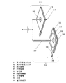
ここで、放電電極17にプラスの電圧を印加した場合について図5を用いて説明を行う。
Here, the case where a positive voltage is applied to the
図2の空気清浄装置1を運転し、放電電極17とアースに接続された対向電極14間に電源部20によりプラス約3〜10KVが印加されると、放電電極17先端近傍に強い電界域が形成され、電界域内の空気を電離させる。このとき発生した電子が空気中の窒素分子および酸素分子に衝突し、窒素分子および酸素分子からは衝突した電子の個数以上の電子が飛び出し、電子を失った窒素分子および酸素分子は正イオンとなる。
When the air purifying apparatus 1 of FIG. 2 is operated and about 3 to 10 KV plus is applied by the
分子から飛び出した電子のいくらかは酸素分子と結合して酸素の負イオンとなり、酸素の負イオンは周辺の分子と反応して別の様々な負イオンを生成しながら電子とともに放電電極17に吸収される。窒素および酸素の正イオンは水分子と反応して別の様々な正イオン生成し、それらは対向電極14の半導電部18に向かい、図5の点線で示す電気力線上を移動する。この状態がコロナ放電である。
Some of the electrons that have jumped out of the molecule are combined with oxygen molecules to become negative ions of oxygen, and the negative ions of oxygen react with neighboring molecules to generate other various negative ions and are absorbed by the
また、放電電極17の先端からは、イオン風と呼ばれる気流が発生しており(図5中の破線矢印)、前述した窒素、酸素、水に由来の正イオンは、このイオン風により最初は半導電部18から遠ざかり、その後、半導電部18に吸い寄せられるため、図5に示したような放物線を描く電気力線上を移動する。
Further, an air flow called an ionic wind is generated from the tip of the discharge electrode 17 (broken arrows in FIG. 5), and the positive ions derived from nitrogen, oxygen, and water described above are initially half-flowed by this ionic wind. Since it is moved away from the
このコロナ放電状態で、送風手段6による送風が、図2では放電ユニット7の下から、図5では放電ユニット7の右から、電気力線上を移動する酸素の正イオンに当たることにより、電気力線上を移動する酸素の正イオンの半数以上が、図5に示すように、送風された風に乗って放電ユニット7から放出される。
In this corona discharge state, air blown by the air blowing means 6 hits the positive ions of oxygen moving on the electric field lines from below the
ここで、放電電極17の先端は、孔部21の略中心軸上に配置されているため、放電電極17と電源接続部19に電気的に接続された半導電部18に高電圧が印加された場合、放電電極17と半導電部18間をながれる電流は、半導電部18の孔部21外周面から導電部23を介して、電源接続部19に到達する。
Here, since the tip of the
つまり、放電電極17を中心として円周方向の周囲に半導電部18が位置するので、半導電部18の広い範囲に電流が分散することになり、半導電部18近傍の空気には広い範囲で発熱による近傍空気の対流作用が起こり、暖められた空気は上昇するため、図5では、放電電極17先端近傍に発生した窒素、酸素、水に由来の正イオンが下降しにくくなり、結果として、半導電部18に吸収されず送風された風に乗って放電ユニット7から放出される窒素、酸素、水に由来の正イオン量を増加させることができるものである。
That is, since the
ここで、3〜10KV電圧を印加することによって、十分なイオン量を発生させることができる。10kV以上でもイオンは発生するが、放電針の劣化などの副作用が生じるため10kV以下で使用することが望ましい。また、3kV未満では放電が不安定になる場合があるため、3kV以上で使用することが望ましい。 Here, a sufficient amount of ions can be generated by applying a voltage of 3 to 10 KV. Although ions are generated even at 10 kV or higher, side effects such as deterioration of the discharge needle occur, so it is desirable to use at 10 kV or lower. Moreover, since discharge may become unstable if it is less than 3 kV, it is desirable to use it at 3 kV or more.
また、本実施の形態では、図2に示すように、放電ユニット7の下流側(排気口4側)に静電霧化ユニット8を設けている。静電霧化ユニット8は、放電電極と、放電電極に対向して位置する対向電極と、放電電極に水を供給する供給手段とを備え、放電電極と対向電極との間に高電圧を印加することで放電電極に保持される水を霧化させてナノメータサイズで強い電荷を持つ帯電微粒子水(マイナスイオンミストで、以下、これをナノイオンミストという)を発生させるものである。ナノイオンミストの粒径は3〜数十nm程度であって、広範囲に飛散し、滞留時間が長く、壁面などの内部にも浸透し、高い脱臭効果や、ダニや花粉等のアレルゲンの不活性化効果や殺菌効果を発揮することができるものである。
Moreover, in this Embodiment, as shown in FIG. 2, the
この静電霧化ユニット8の上流側に放電ユニット7を有することで、放電ユニット7で発生させた酸素の正イオンにより、空気中のダニや花粉等のアレルゲンおよび浮遊カビ菌や浮遊菌などの汚れを+に帯電させ、マイナスイオンである、ナノイオンミストが接触しやすくできる。
By having the
すなわち、放電ユニット7で発生させた酸素の正イオンは、ナノイオンミストの不活性化効果や殺菌効果を向上させる、アシストイオンとして作用する。
That is, the positive ions of oxygen generated by the
図6は、空気清浄装置1の制御回路のブロック図である。図2の空間部11に電源部20を含む制御部25が収納されており、放電ユニット7、静電霧化ユニット8に対し、それぞれ各ユニットに高電圧を印加する第1の高電圧発生手段26、第2の高電圧発生手段27が接続され、各高電圧発生手段は制御手段28に接続されている。
FIG. 6 is a block diagram of a control circuit of the air cleaning device 1. A
また、制御手段28には、運転操作スイッチ29と送風手段6(実際は電動機12)も接続されており、運転操作スイッチ29からの入力により、制御手段28は、送風手段6、第1の高電圧発生手段26、第2の高電圧発生手段27を制御している。
Further, the operation means
本実施形態では、放電ユニット7、静電霧化ユニット8に対し、別々の高電圧発生手段を用いたが、同じ高電圧を発生させる場合には、一つの高電圧発生手段を共用できる。
In the present embodiment, separate high voltage generation means are used for the
このような制御部25を備えた空気清浄装置1を運転操作スイッチ29を操作して運転することにより、制御手段28からの制御信号を受けて、第1の高電圧発生手段26、第2の高電圧発生手段27、送風手段6が作動し、排気口4から静電霧化ユニット8から発生したナノイオンミストと、放電ユニット7から発生したアシストイオンが室内へ放出される。
By operating the air purifying apparatus 1 having such a
その結果、前述したナノイオンミストの効果を発揮できる。すなわち、空気中の菌を不活化することができる。また、空気中の臭いを分解して取り除くことで、脱臭効果を発揮させることができる。また、ナノイオンミストを含む空気を衣類やカーテン等にあてることによって、衣類やカーテンの脱臭・除菌などの効果が期待できる。 As a result, the effect of the nano ion mist described above can be exhibited. That is, bacteria in the air can be inactivated. Moreover, the deodorizing effect can be exhibited by decomposing and removing the odor in the air. In addition, by applying air containing nano-ion mist to clothes, curtains, and the like, effects such as deodorization and sterilization of clothes and curtains can be expected.
なお、本実施形態では放電ユニット7が一つの構成を説明したが、多くのイオン量が必要な場合、複数備えてもよい。
In addition, although the
(実施の形態2)
実施の形態1では、放電電極17にプラスの電圧を印加し静電霧化ユニット8との併用で発生させたイオンをアシストイオンとして利用したが、本実施形態では、放電電極17にマイナスの電圧を印加し、単独でマイナスイオンとして利用する場合について説明する。
(Embodiment 2)
In the first embodiment, a positive voltage is applied to the
実施の形態1と同じ構成は、同一番号を付し、詳細な説明は省略する。 The same configurations as those in the first embodiment are denoted by the same reference numerals, and detailed description thereof is omitted.
放電電極17にマイナスの電圧を印加した場合について図5を用いて説明を行う。
The case where a negative voltage is applied to the
図2の空気清浄装置1(静電霧化ユニット8は備えていない)を運転し、放電電極17とアースに接続された対向電極14間に電源部20によりマイナス約3〜10KVが印加されると、放電電極17先端近傍に強い電界域が形成され、電界域内の空気を電離させる。このとき、放電電極17からは電子が放出され、空気中の窒素分子および酸素分子に衝突し、窒素分子および酸素分子から、衝突した電子の個数以上の電子が飛び出し、電子を失った窒素分子および酸素分子は正イオンとなる。窒素および酸素の正イオンは水分子と反応して別の様々な正イオン生成しながら放電電極17へ吸収される。一方、分子から飛び出した電子のいくらかは酸素分子と結合して酸素の負イオンとなり、周辺の分子と反応して別の様々な負イオンを生成しながら電子とともに対向電極14の半導電部18に向かう。
The air purifying apparatus 1 of FIG. 2 (the
このように発生した負イオンを実施の形態1と同様に空気清浄装置1の排気口4から室内へ放出することにより、負イオン特有の爽快感(滝の近くの清々しさ)を使用者に感じさせられるという効果を奏する。
The negative ions generated in this manner are discharged into the room from the
なお、実施の形態1の構成で、静電霧化ユニット8を作動させず、放電電極17にマイナスの電圧を印加して放電ユニット7を作動させた場合、本実施形態と同様の作用効果を有する。
In the configuration of the first embodiment, when the
(実施の形態3)
本実施形態は、放電ユニットを、イオンを発生させる第1の放電ユニット31と、活性種を発生させる第2の放電ユニット32で構成したものである。第1の放電ユニット31は実施の形態1で述べた形態である。実施の形態1、2と同じ構成は、同一番号を付し、詳細な説明は省略する。
(Embodiment 3)
In the present embodiment, the discharge unit includes a
第2の放電ユニット32は、図7に示すように絶縁性基板36と、絶縁性基板36の放電電極33先端側の表面に設けた半導電部37と、この半導電部37の外周縁に設けた導電部35とからなる対向電極34と、絶縁性基板36の円形の孔部38を貫通することなく配置された放電電極33と、導電部35と電気的に接続された電源接続部39と、この電源接続部39および放電電極33に電圧を印加する電源部20(図2に記載)とから形成している。
As shown in FIG. 7, the
図8に示すように、放電電極33の先端は絶縁性基板36の表面からは離間して対向配置する。絶縁性基板36の円形の孔部38は設けなくてもコロナ放電は可能だが、設けた方が、コロナ放電によって発生するイオン風が、放電電極33の先端から孔部38を通過するという効果がある。放電電極33の先端は、孔部38の中心線上にあれば、コロナ放電が均一に発生する。
As shown in FIG. 8, the tip of the
第1の放電ユニット31も第2の放電ユニット32も、電極部材を、実施の形態1で記述したような支持部材によって固定できるので、図7では支持部材は記載せず、ここでの説明も省略する。
In both the
第2の放電ユニット32において、図8に示すように、高電圧が印加された放電電極33の先端から半導電部37に向かう電気力線は、点線のようになる。この構成では、放電電極33の先端が、孔部38を貫通して突出している場合に比べてイオンの発生量が少なく、オゾンなどの活性種がより多く発生する。
In the
すなわち、通常のコロナ放電でオゾンなどの活性種や実施の形態1で説明したイオンが発生するが、放電電極33の先端と半導電部37の位置関係でイオンと活性種の発生割合が変わるのである。この理由を以下で説明する。
That is, active species such as ozone and ions described in the first embodiment are generated in a normal corona discharge, but the generation ratio of ions and active species varies depending on the positional relationship between the tip of the
第1の放電ユニット31と第2の放電ユニット32のそれぞれの電極間距離(放電電極33の先端と半導電部37との直交方向の距離)が同じで、放電極への印加電圧が同じ場合、第2の放電ユニット32の方が放電量は多くなる。これは放電電極33の先端が、孔部38を貫通して突出している場合は、図5に示すように電気力線が半導電部に向かって湾曲しているために、電流が流れにくくなっているものと考えられる。
When the distance between the electrodes of the
オゾンなどの活性種は、電流が増加するとそれらの量も増加することが分かっている。ゆえに同電極間距離・同電圧でより電流が流れやすい第2の放電ユニット32の方が第1の放電ユニット31に比べ、オゾンなどの活性種がより多く発生する。また、第2の放電ユニットの構成上、放電により発生したイオンはすぐに半導電部37に引き寄せられるため、第1の放電ユニット31に比べ、イオン量は少なくなる。
Active species such as ozone have been shown to increase in amount as current increases. Therefore, more active species such as ozone are generated in the
したがって、第1の放電ユニット31はイオンの発生に効果的な構成であり、第2の放電ユニット32は、活性種の発生に効果的な構成である。第1の放電ユニット31又は第2の放電ユニット32をそれぞれ複数備えることは可能で、例えば、より多くのイオンを発生させるために、第1の放電ユニット31を2つ以上設けたり、より多くの活性種を発生させるために、第2の放電ユニット32を2つ以上設けたりすることも可能である。
Therefore, the
第1の放電ユニット31と第2の放電ユニット32を構成する電極部材はすべて同一でもよく、その場合、両者の間で異なる点は、放電電極先端の位置だけとなる。すなわち、共通の部品を用いて2通りの放電ユニットを構築することが可能であり、製造コストに関して合理的である。
The electrode members constituting the
また、それぞれのユニットを個別の電源部20に接続してもよいが、1つの電源部20に両方のユニットを接続して同じ高電圧を印加することも可能であり、合理的な設計が可能となる。
In addition, each unit may be connected to an individual
(実施の形態4)
本実施の形態は、図9に示すように、針状の放電電極43の両先端が傾斜部を有して、第1の放電ユニット41と第2の放電ユニット42で放電電極43を共用するものである。実施の形態1〜3と同じ構成は、同一番号を付し、詳細な説明は省略する。
(Embodiment 4)
In the present embodiment, as shown in FIG. 9, both ends of the needle-
第1の放電ユニット41は、対向電極14の絶縁性基板16の孔部21を、放電電極43の第1の先端部44が貫通するように配置して構成され、第2の放電ユニット42は、対向電極34の絶縁性基板36の孔部38を放電電極43の第2の先端部45が貫通しないように、放電電極43を孔部38に対向配置して構成される。
The
放電電極43は電源部20と接続し、第1の放電ユニット41と第2の放電ユニット42は同じ電圧が印加され、第1の放電ユニット41からは多くのイオンが発生し、第2の放電ユニット42からは多くの活性種が発生する。
The
この構成においては、1つの放電電極43で2つの放電ユニットでコロナ放電させることができ、部品点数が少なく小型化が可能となる。
In this configuration, corona discharge can be performed by two discharge units with one
(実施の形態5)
本実施の形態は、1つの対向電極を第1の放電ユニット51と第2の放電ユニット52が共用する形態である。実施の形態1〜実施の形態4と同じ構成は、同一番号を付し、詳細な説明は省略する。
(Embodiment 5)
In the present embodiment, one counter electrode is shared by the
図10に示すように、絶縁性基板53の表面上に半導電部55と孔部21と孔部38、半導電部55上に図3の貫通孔24を有する導電部54を設け、孔部21を貫通するように放電電極17を配置し、孔部38の中心線上に、孔部38を貫通しないように放電電極33を配置し、孔部21と放電電極17の組合せの方を第1の放電ユニット51、孔部38と放電電極33の組合せの方を第2の放電ユニット52とする。
As shown in FIG. 10, the
放電電極17と放電電極33は1つの電源部20に接続しても、それぞれ個別の電源部20を設けて接続してもどちらでもよい。
The
この構成においては、絶縁性基板と導電部で構成する対向電極を1つに統一できるため、実施の形態4と同様、部品点数が少なく小型化が可能となる。 In this configuration, since the counter electrode formed of the insulating substrate and the conductive portion can be unified, the number of components is small and the size can be reduced as in the fourth embodiment.
以上のように本発明は、放電電極と対向電極に電源部から電圧を印加してコロナ放電させる放電ユニットにおいて、前記放電電極は針状電極であり、前記対向電極は平板状で、この平板状の対向電極に対して前記針状の放電電極を非接触で、直交に、かつ、その先端を突出させて配置し、前記放電電極の先端が突出した側の、前記対向電極の表面が、半導電性を有する構成としたものであるので、放電のスパークを防止しつつ放電電極と対向電極の距離を近づけ、活性種の発生量を増やすことができる。 As described above, the present invention relates to a discharge unit in which a voltage is applied to a discharge electrode and a counter electrode from a power supply unit to perform corona discharge. The discharge electrode is a needle-like electrode, the counter electrode has a flat plate shape, and the flat plate shape. The needle-like discharge electrode is arranged in a non-contact, orthogonal, and projecting tip with respect to the counter electrode, and the surface of the counter electrode on the side where the tip of the discharge electrode projects is half Since the structure has conductivity, it is possible to increase the amount of active species generated by reducing the distance between the discharge electrode and the counter electrode while preventing discharge sparks.
すなわち、本発明においては、半導電部と放電電極に電源部から電圧を印加してコロナ放電により活性種を発生させる構成としたことにより、半導電部と放電電極の距離を近くでき、その結果放電電流が増えるため、イオンの発生量を増やすことができる。 That is, in the present invention, by applying a voltage from the power supply unit to the semiconductive portion and the discharge electrode to generate active species by corona discharge, the distance between the semiconductive portion and the discharge electrode can be reduced. Since the discharge current increases, the amount of ions generated can be increased.
したがって、放電ユニットおよびこれを用いた空気清浄装置としての活用が期待される。 Therefore, utilization as a discharge unit and an air purifier using the same is expected.
1 空気清浄装置
2 エアフィルタ
3 吸気口
4 排気口
5 本体
6 送風手段
7 放電ユニット
8 静電霧化ユニット
9 仕切板部
10 風路部
11 空間部
12 電動機
13 羽根部
14 対向電極
16 絶縁性基板
17 放電電極
18 半導電部
19 電源接続部
20 電源部
21 孔部
22 支持部材
22a 固定蓋
22b 台座
22c 底板
23 導電部
24 貫通孔
25 制御部
26 第1の高電圧発生手段
27 第2の高電圧発生手段
28 制御手段
29 運転操作スイッチ
31 第1の放電ユニット
32 第2の放電ユニット
33 放電電極
34 対向電極
35 導電部
36 絶縁性基板
37 半導電部
38 孔部
39 電源接続部
41 第1の放電ユニット
42 第2の放電ユニット
43 放電電極
44 第1の先端部
45 第2の先端部
51 第1の放電ユニット
52 第2の放電ユニット
53 絶縁性基板
54 導電部
55 半導電部
DESCRIPTION OF SYMBOLS 1
Claims (12)
前記放電電極は針状で、
前記対向電極は平板状で、この平板状の対向電極に対して前記針状の放電電極を非接触で、
直交に、かつ、その先端を突出させて配置し、
前記放電電極の先端が突出した側の、前記対向電極の表面が、半導電性を有することを特徴とした放電ユニット。 In the discharge unit that applies a voltage from the power supply unit to the discharge electrode and the counter electrode to cause corona discharge,
The discharge electrode is needle-shaped,
The counter electrode is flat, and the needle-like discharge electrode is not contacted with the flat counter electrode.
Orthogonally and with its tip protruding,
The discharge unit characterized in that the surface of the counter electrode on the side from which the tip of the discharge electrode protrudes has semiconductivity.
各々の放電電極と対向電極に同一電源部から電圧を印加してコロナ放電させる放電ユニットにおいて、
少なくとも一つの前記放電ユニットの前記放電電極と前記対向電極の位置関係は、
前記対向電極が、前記放電電極の先端側近傍で、前記放電電極の略垂直方向に対向配置されたことを特徴とした放電ユニット。 A plurality of the discharge units according to claim 1 are provided,
In the discharge unit that applies corona discharge by applying a voltage from the same power supply to each discharge electrode and the counter electrode,
The positional relationship between the discharge electrode and the counter electrode of at least one of the discharge units is:
A discharge unit, wherein the counter electrode is disposed in the vicinity of the distal end side of the discharge electrode so as to face the discharge electrode in a substantially vertical direction.
この本体内に送風手段と静電霧化手段と請求項7記載の放電ユニットとを設け、
前記送風手段により前記本体の吸気口から吸込んだ空気を、前記静電霧化手段と前記放電ユニットに送り、
前記静電霧化手段で発生した活性種と、前記放電ユニットで発生したプラスイオンを含んだ空気を前記排気口から吹出す構成としたことを特徴とする空気清浄装置。 A body having an air inlet and an air outlet;
In the main body, air blowing means, electrostatic atomizing means and the discharge unit according to claim 7 are provided,
The air sucked from the air inlet of the main body by the blowing means is sent to the electrostatic atomizing means and the discharge unit,
An air cleaning device characterized in that air containing active species generated by the electrostatic atomization means and positive ions generated by the discharge unit is blown out from the exhaust port.
この本体内に送風手段と請求項8記載の放電ユニットとを設け、
前記送風手段により前記本体の吸気口から吸込んだ空気を、前記放電ユニットに送り、
前記放電ユニットで発生したマイナスイオンを含んだ空気を前記排気口から吹出す構成としたことを特徴とする空気清浄装置。 A body having an air inlet and an air outlet;
In the main body, air blowing means and the discharge unit according to claim 8 are provided,
The air sucked from the air inlet of the main body by the blowing means is sent to the discharge unit,
An air cleaning apparatus characterized in that air containing negative ions generated in the discharge unit is blown out from the exhaust port.
Priority Applications (3)
| Application Number | Priority Date | Filing Date | Title |
|---|---|---|---|
| JP2012213655A JP6002934B2 (en) | 2012-06-27 | 2012-09-27 | Discharge unit and air purifier using the same |
| CN201380034190.2A CN104428012B (en) | 2012-06-27 | 2013-06-21 | Discharge cell and employ its air cleaner |
| PCT/JP2013/003883 WO2014002453A1 (en) | 2012-06-27 | 2013-06-21 | Electricity discharging unit and air cleaning device using same |
Applications Claiming Priority (3)
| Application Number | Priority Date | Filing Date | Title |
|---|---|---|---|
| JP2012143737 | 2012-06-27 | ||
| JP2012143737 | 2012-06-27 | ||
| JP2012213655A JP6002934B2 (en) | 2012-06-27 | 2012-09-27 | Discharge unit and air purifier using the same |
Publications (2)
| Publication Number | Publication Date |
|---|---|
| JP2014029821A JP2014029821A (en) | 2014-02-13 |
| JP6002934B2 true JP6002934B2 (en) | 2016-10-05 |
Family
ID=50202261
Family Applications (1)
| Application Number | Title | Priority Date | Filing Date |
|---|---|---|---|
| JP2012213655A Active JP6002934B2 (en) | 2012-06-27 | 2012-09-27 | Discharge unit and air purifier using the same |
Country Status (1)
| Country | Link |
|---|---|
| JP (1) | JP6002934B2 (en) |
Families Citing this family (5)
| Publication number | Priority date | Publication date | Assignee | Title |
|---|---|---|---|---|
| JP5896069B1 (en) * | 2014-09-19 | 2016-03-30 | ダイキン工業株式会社 | Discharge unit |
| CN109477650A (en) | 2016-07-05 | 2019-03-15 | 布鲁雅尔公司 | Air cleaning tent |
| TWI601919B (en) * | 2016-07-11 | 2017-10-11 | 馗鼎奈米科技股份有限公司 | Plasma purification module |
| JP7145424B2 (en) * | 2018-08-29 | 2022-10-03 | パナソニックIpマネジメント株式会社 | discharge device |
| CN113048619B (en) * | 2021-04-25 | 2022-03-01 | 珠海格力电器股份有限公司 | Air purifier control method, storage medium and air purifier |
Family Cites Families (3)
| Publication number | Priority date | Publication date | Assignee | Title |
|---|---|---|---|---|
| JP4386376B2 (en) * | 2007-01-23 | 2009-12-16 | 九州日立マクセル株式会社 | Ion generator |
| JP2011233301A (en) * | 2010-04-26 | 2011-11-17 | Sharp Corp | Ion generating device and electrical apparatus |
| JP2012134000A (en) * | 2010-12-21 | 2012-07-12 | Sharp Corp | Ion generating device and ion generating device cleaning method |
-
2012
- 2012-09-27 JP JP2012213655A patent/JP6002934B2/en active Active
Also Published As
| Publication number | Publication date |
|---|---|
| JP2014029821A (en) | 2014-02-13 |
Similar Documents
| Publication | Publication Date | Title |
|---|---|---|
| JP6002934B2 (en) | Discharge unit and air purifier using the same | |
| JP4945008B2 (en) | Ion generator, electrical equipment | |
| JP4063784B2 (en) | Ion generator, ion generator | |
| CN104428012B (en) | Discharge cell and employ its air cleaner | |
| JP2007305606A5 (en) | ||
| WO2010122862A1 (en) | Ion generator and air conditioner | |
| JP2006198502A (en) | Antistatic atomizer | |
| WO2014002453A1 (en) | Electricity discharging unit and air cleaning device using same | |
| JP2014121424A (en) | Discharge unit and air cleaner using the same | |
| JP6043944B2 (en) | Active species generating unit and active species generating apparatus using the same | |
| JP2014044888A (en) | Discharge unit and air cleaning apparatus using the same | |
| JP5118241B1 (en) | Ion generator and air purifier equipped with the same | |
| JP4683149B2 (en) | Discharge unit for liquid treatment and humidity control device | |
| JP5974269B2 (en) | Active species generating unit and active species generating apparatus using the same | |
| JP5974273B2 (en) | Active species generating unit and active species generating apparatus using the same | |
| WO2013121669A1 (en) | Ion-generating element and ion generator provided with same | |
| JP2020078516A (en) | Air cleaner | |
| JP5810259B2 (en) | Active species generator | |
| JP2002343534A (en) | Ion generating element and air conditioning device having the same | |
| JP2005230568A (en) | Air purifier or deodorizer | |
| JP5899398B2 (en) | Active species generating unit and active species generating apparatus using the same | |
| JP5974272B2 (en) | Active species generating unit and active species generating apparatus using the same | |
| JP2013000531A (en) | Active species generation device | |
| JP2013034516A (en) | Active species generating apparatus | |
| JP2006164767A (en) | Ion generator |
Legal Events
| Date | Code | Title | Description |
|---|---|---|---|
| A711 | Notification of change in applicant |
Free format text: JAPANESE INTERMEDIATE CODE: A711 Effective date: 20141003 |
|
| A621 | Written request for application examination |
Free format text: JAPANESE INTERMEDIATE CODE: A621 Effective date: 20150925 |
|
| RD01 | Notification of change of attorney |
Free format text: JAPANESE INTERMEDIATE CODE: A7421 Effective date: 20160518 |
|
| TRDD | Decision of grant or rejection written | ||
| A01 | Written decision to grant a patent or to grant a registration (utility model) |
Free format text: JAPANESE INTERMEDIATE CODE: A01 Effective date: 20160726 |
|
| A61 | First payment of annual fees (during grant procedure) |
Free format text: JAPANESE INTERMEDIATE CODE: A61 Effective date: 20160808 |
|
| R151 | Written notification of patent or utility model registration |
Ref document number: 6002934 Country of ref document: JP Free format text: JAPANESE INTERMEDIATE CODE: R151 |