JP5971635B2 - Vector unit sharing apparatus and method - Google Patents
Vector unit sharing apparatus and method Download PDFInfo
- Publication number
- JP5971635B2 JP5971635B2 JP2013550709A JP2013550709A JP5971635B2 JP 5971635 B2 JP5971635 B2 JP 5971635B2 JP 2013550709 A JP2013550709 A JP 2013550709A JP 2013550709 A JP2013550709 A JP 2013550709A JP 5971635 B2 JP5971635 B2 JP 5971635B2
- Authority
- JP
- Japan
- Prior art keywords
- unit
- processor
- vector
- units
- control
- Prior art date
- Legal status (The legal status is an assumption and is not a legal conclusion. Google has not performed a legal analysis and makes no representation as to the accuracy of the status listed.)
- Active
Links
- 239000013598 vector Substances 0.000 title claims description 376
- 238000000034 method Methods 0.000 title claims description 53
- 238000012545 processing Methods 0.000 claims description 227
- 230000008569 process Effects 0.000 claims description 27
- 230000008859 change Effects 0.000 claims description 5
- 230000008878 coupling Effects 0.000 claims 1
- 238000010168 coupling process Methods 0.000 claims 1
- 238000005859 coupling reaction Methods 0.000 claims 1
- 238000010586 diagram Methods 0.000 description 30
- 230000006870 function Effects 0.000 description 16
- 230000008901 benefit Effects 0.000 description 4
- 238000013461 design Methods 0.000 description 2
- 238000001514 detection method Methods 0.000 description 2
- 238000003702 image correction Methods 0.000 description 1
- 238000012986 modification Methods 0.000 description 1
- 230000004048 modification Effects 0.000 description 1
- 238000012546 transfer Methods 0.000 description 1
Images


Classifications
-
- G—PHYSICS
- G06—COMPUTING; CALCULATING OR COUNTING
- G06F—ELECTRIC DIGITAL DATA PROCESSING
- G06F15/00—Digital computers in general; Data processing equipment in general
- G06F15/76—Architectures of general purpose stored program computers
-
- G—PHYSICS
- G06—COMPUTING; CALCULATING OR COUNTING
- G06F—ELECTRIC DIGITAL DATA PROCESSING
- G06F15/00—Digital computers in general; Data processing equipment in general
- G06F15/76—Architectures of general purpose stored program computers
- G06F15/78—Architectures of general purpose stored program computers comprising a single central processing unit
- G06F15/7867—Architectures of general purpose stored program computers comprising a single central processing unit with reconfigurable architecture
-
- G—PHYSICS
- G06—COMPUTING; CALCULATING OR COUNTING
- G06F—ELECTRIC DIGITAL DATA PROCESSING
- G06F9/00—Arrangements for program control, e.g. control units
- G06F9/06—Arrangements for program control, e.g. control units using stored programs, i.e. using an internal store of processing equipment to receive or retain programs
- G06F9/30—Arrangements for executing machine instructions, e.g. instruction decode
- G06F9/30003—Arrangements for executing specific machine instructions
- G06F9/30007—Arrangements for executing specific machine instructions to perform operations on data operands
- G06F9/30036—Instructions to perform operations on packed data, e.g. vector, tile or matrix operations
-
- G—PHYSICS
- G06—COMPUTING; CALCULATING OR COUNTING
- G06F—ELECTRIC DIGITAL DATA PROCESSING
- G06F15/00—Digital computers in general; Data processing equipment in general
- G06F15/76—Architectures of general purpose stored program computers
- G06F15/80—Architectures of general purpose stored program computers comprising an array of processing units with common control, e.g. single instruction multiple data processors
- G06F15/8007—Architectures of general purpose stored program computers comprising an array of processing units with common control, e.g. single instruction multiple data processors single instruction multiple data [SIMD] multiprocessors
-
- G—PHYSICS
- G06—COMPUTING; CALCULATING OR COUNTING
- G06F—ELECTRIC DIGITAL DATA PROCESSING
- G06F15/00—Digital computers in general; Data processing equipment in general
- G06F15/76—Architectures of general purpose stored program computers
- G06F15/80—Architectures of general purpose stored program computers comprising an array of processing units with common control, e.g. single instruction multiple data processors
- G06F15/8053—Vector processors
- G06F15/8076—Details on data register access
- G06F15/8084—Special arrangements thereof, e.g. mask or switch
-
- G—PHYSICS
- G06—COMPUTING; CALCULATING OR COUNTING
- G06F—ELECTRIC DIGITAL DATA PROCESSING
- G06F15/00—Digital computers in general; Data processing equipment in general
- G06F15/76—Architectures of general purpose stored program computers
- G06F15/80—Architectures of general purpose stored program computers comprising an array of processing units with common control, e.g. single instruction multiple data processors
- G06F15/8053—Vector processors
- G06F15/8092—Array of vector units
-
- G—PHYSICS
- G06—COMPUTING; CALCULATING OR COUNTING
- G06F—ELECTRIC DIGITAL DATA PROCESSING
- G06F9/00—Arrangements for program control, e.g. control units
- G06F9/06—Arrangements for program control, e.g. control units using stored programs, i.e. using an internal store of processing equipment to receive or retain programs
- G06F9/30—Arrangements for executing machine instructions, e.g. instruction decode
- G06F9/30098—Register arrangements
- G06F9/30105—Register structure
- G06F9/30112—Register structure comprising data of variable length
-
- G—PHYSICS
- G06—COMPUTING; CALCULATING OR COUNTING
- G06F—ELECTRIC DIGITAL DATA PROCESSING
- G06F9/00—Arrangements for program control, e.g. control units
- G06F9/06—Arrangements for program control, e.g. control units using stored programs, i.e. using an internal store of processing equipment to receive or retain programs
- G06F9/30—Arrangements for executing machine instructions, e.g. instruction decode
- G06F9/38—Concurrent instruction execution, e.g. pipeline, look ahead
- G06F9/3867—Concurrent instruction execution, e.g. pipeline, look ahead using instruction pipelines
-
- G—PHYSICS
- G06—COMPUTING; CALCULATING OR COUNTING
- G06F—ELECTRIC DIGITAL DATA PROCESSING
- G06F9/00—Arrangements for program control, e.g. control units
- G06F9/06—Arrangements for program control, e.g. control units using stored programs, i.e. using an internal store of processing equipment to receive or retain programs
- G06F9/30—Arrangements for executing machine instructions, e.g. instruction decode
- G06F9/38—Concurrent instruction execution, e.g. pipeline, look ahead
- G06F9/3885—Concurrent instruction execution, e.g. pipeline, look ahead using a plurality of independent parallel functional units
- G06F9/3887—Concurrent instruction execution, e.g. pipeline, look ahead using a plurality of independent parallel functional units controlled by a single instruction for multiple data lanes [SIMD]
Landscapes
- Engineering & Computer Science (AREA)
- Theoretical Computer Science (AREA)
- Computer Hardware Design (AREA)
- Physics & Mathematics (AREA)
- General Engineering & Computer Science (AREA)
- General Physics & Mathematics (AREA)
- Software Systems (AREA)
- Mathematical Physics (AREA)
- Image Processing (AREA)
- Advance Control (AREA)
- Complex Calculations (AREA)
Description
本発明の開示は、画像処理またはデータ処理に関し、より具体的には再構成可能ベクトルデータ処理装置を提供するプロセッサに関する。 The present disclosure relates to image processing or data processing, and more particularly to a processor that provides a reconfigurable vector data processing apparatus.
画像処理は計算上複雑であり、幾つかの用途においては専用のプロセッサまたは処理技術から恩恵を受ける。リアルタイムに(または略リアルタイムで)画像情報を処理するため、設計用および画像用の専用プロセッサによる様々な処理技術が使用されている。例えば、あるプロセッサは、1つのスカラー・プロセッシング・ユニットと、複数個の情報に対する命令を一度に実行可能な1若しくはそれ以上のベクトル・プロセッシング・ユニットとを含む。特にベクトル処理能力が供給された処理作業にマッチするとき、ベクトル・プロセッシング・ユニットの使用により、処理効率を高めることが可能である。 Image processing is computationally complex and in some applications benefits from dedicated processors or processing techniques. In order to process image information in real time (or almost in real time), various processing techniques using dedicated processors for design and images are used. For example, a processor includes a scalar processing unit and one or more vector processing units that can execute instructions for multiple pieces of information at once. The processing efficiency can be increased by using a vector processing unit, especially when the vector processing capability matches the supplied processing operation.
ベクトルユニットの使用により効率が改善されたが、従来のベクトルユニットは、各ベクトルユニットに伴う演算ユニット(computational units:CUs)の処理幅が固定であった。このため、ベクトルユニットで処理される作業の幅と同等でなかった場合、またはその逆の場合も、非効率的なプロセッサ利用率または低い実行性能が生じる可能性がある。 Although the efficiency is improved by using the vector unit, the conventional vector unit has a fixed processing width of the computation units (CUs) associated with each vector unit. For this reason, an inefficient processor utilization rate or low execution performance may occur even when the width of the work processed by the vector unit is not equivalent, or vice versa.
従って、プロセッサで共有される改善されたベクトルユニットが必要とされている。
この出願の発明に関連する先行技術文献情報としては、以下のものがある(国際出願日以降国際段階で引用された文献及び他国に国内移行した際に引用された文献を含む)。
(先行技術文献)
(特許文献)
(特許文献1) 米国特許第4,633,389号明細書
(特許文献2) 米国特許第6,317,819号明細書
(特許文献3) 米国特許第5,430,884号明細書
(特許文献4) 米国特許第7,334,110号明細書
Therefore, there is a need for an improved vector unit shared by processors.
Prior art document information related to the invention of this application includes the following (including documents cited in the international phase after the international filing date and documents cited when entering the country in other countries).
(Prior art documents)
(Patent Literature)
(Patent Document 1) US Pat. No. 4,633,389
(Patent Document 2) US Pat. No. 6,317,819
(Patent Document 3) US Pat. No. 5,430,884
(Patent Document 4) US Pat. No. 7,334,110 Specification
本発明の開示の観点によれば、再構成可能ベクトルプロセッサが提供されており、当該再構成可能ベクトルプロセッサは、複数のプロセッサユニットであって、各プロセッサユニットは命令を解読し、制御信号を生成する制御ユニットと、スカラーデータの命令を処理するスカラーユニットと、前記生成された制御信号に基づいてベクトルデータの命令を処理するベクトルユニットとを有するものである前記複数のプロセッサユニットと、前記複数のプロセッサユニットのうちの1つにより生成された制御信号を、前記複数のプロセッサユニットの異なるプロセッサに関連するベクトルユニットに選択的に提供するベクトル制御セレクタとを有する。 According to an aspect of the present disclosure, a reconfigurable vector processor is provided, wherein the reconfigurable vector processor is a plurality of processor units, each processor unit interpreting instructions and generating control signals A plurality of processor units, a plurality of processor units having a control unit for processing, a scalar unit for processing instructions for scalar data, and a vector unit for processing instructions for vector data based on the generated control signal, A vector control selector for selectively providing a control signal generated by one of the processor units to a vector unit associated with a different processor of the plurality of processor units.
2若しくはそれ以上のプロセッサユニットを有し、各々がベクトルユニットを備えている再構成可能ベクトルプロセッサを使用してデータを処理する方法であって、前記再構成可能ベクトルプロセッサを設定して、第1のサイズのベクトルユニットを提供することにより、第1のサイズのベクトルデータを処理するものである、前記提供する工程と、1若しくはそれ以上の命令を前記第1のサイズのベクトルユニットを使用して実行して、前記第1のサイズのベクトルデータを処理する工程と、前記再構成可能ベクトルプロセッサを再設定して、前記ベクトルユニットのサイズを第2のサイズに変更する工程と、1若しくはそれ以上の命令を前記第2のサイズのベクトルユニットを使用して実行して、前記第2のサイズのベクトルデータを処理する工程とを有する方法。 A method of processing data using a reconfigurable vector processor having two or more processor units, each comprising a vector unit, comprising: By providing a vector unit of a size of the first size vector data by processing the providing step and one or more instructions using the vector unit of the first size. Executing and processing the vector data of the first size; reconfiguring the reconfigurable vector processor to change the size of the vector unit to a second size; and one or more Are executed using the vector unit of the second size to process the vector data of the second size. Method comprising the step of.
更に、特徴および利点は、添付の図面と共に以下の詳細な説明を参照することにより明らかになるであろう。
ベクトルユニット共有の装置、システム、および方法の実施形態は、ほんの一例として図1〜17を参照して記載されている。 Embodiments of vector unit sharing apparatus, systems, and methods are described by way of example only with reference to FIGS.
再構成可能ベクトルプロセッサは、そのベクトルユニットのサイズ変更により、異なるサイズのベクトル処理可能となる。前記再構成可能ベクトルプロセッサは、複数のプロセッサユニットを有する。前記プロセッサユニットの各々は、命令を解読し、制御信号を生成する制御ユニットと、スカラーデータの命令を処理するスカラーユニットと、制御信号の制御下でベクトルデータの命令を処理するベクトルユニットとを有する。前記再構成可能ベクトルプロセッサはまた、前記複数のプロセッサユニットの1つのプロセッサユニットにより生成された制御信号を、前記複数のプロセッサユニットの異なるプロセッサユニットのベクトルユニットに選択的に提供するベクトル制御セレクタを有する。本発明の開示にはプロセッサという用語が使用されているが、プロセッサは、1若しくはそれ以上のコアを有するプロセッサに組み込まれた、独立したスタンドアロンプロセッサとして提供された、または前記ベクトルプロセッサの機能を実行するためマルチ物理プロセッサの間で機能的に分けられたものであってもよい。代替的に、前記ベクトルプロセッサは多数の物理的実装に記入された機能特性を実施するために利用されるプロセッサアーキテクチャを定義することも可能である。 The reconfigurable vector processor can process vectors of different sizes by changing the size of the vector unit. The reconfigurable vector processor has a plurality of processor units. Each of the processor units includes a control unit that decodes an instruction and generates a control signal, a scalar unit that processes an instruction of scalar data, and a vector unit that processes an instruction of vector data under the control of the control signal. . The reconfigurable vector processor also includes a vector control selector that selectively provides control signals generated by one processor unit of the plurality of processor units to vector units of different processor units of the plurality of processor units. . Although the term processor is used in the present disclosure, the processor is provided as an independent stand-alone processor embedded in a processor having one or more cores, or performs the functions of the vector processor. Therefore, it may be functionally divided among multiple physical processors. Alternatively, the vector processor can define a processor architecture that is utilized to implement functional characteristics written in multiple physical implementations.
図1Aは、スカラー100をブロック図で示している。前記スカラー100は、処理可能な様々なデータを表すのに使用される。例えば、前記スカラー100は、画像の一部の色の純度を表すのに使用される。前記スカラー100は、複数のビットを有する。前記スカラ100は、8ビット幅を有するものとして図示されているが、使用されるプロセッサのアーキテクチャに応じて他の幅のスカラーも可能であることは理解されたい。例えば、スカラーは、4ビット、8ビット(一般に1バイトと呼ばれる)、16ビット、32ビット、64ビットなどがある。 FIG. 1A shows a scalar 100 in a block diagram. The scalar 100 is used to represent various data that can be processed. For example, the scalar 100 is used to indicate the purity of a part of the image. The scalar 100 has a plurality of bits. Although the scalar 100 is illustrated as having an 8-bit width, it should be understood that other width scalars are possible depending on the processor architecture used. For example, the scalar includes 4 bits, 8 bits (generally called 1 byte), 16 bits, 32 bits, 64 bits, and the like.
図1Bは、ベクトル120をブロック図で示している。前記ベクトル120は、複数のスカラーデータ122、124、126、128を有する。一般に、前記ベクトル120の各スカラー122、124、126、128は、同一幅を有し、それは例えば8ビットである。ベクトル110は、スカラー122、124、126、128を有する4つのベクトルサイズを有するものとして図示されている。前記ベクトルが異なるサイズでも可能であることは理解されたい。例えば、ベクトルは、0〜「サイズ()−1」で番号付けされた1若しくはそれ以上のスカラーから構成されることが可能である。前記ベクトルを有する前記スカラーの幅はまた、様々である。例えば、第1のベクトルは4つのスカラーから構成させれ、各々は8ビット幅であり、第2のベクトルは2スカラーから構成され、各々は16ビット幅であり、そして、第3のベクトルは1スカラーから構成され、32ビット幅である。
FIG. 1B shows the
ベクトルの全幅は、ベクトルのスカラーの幅を合計したものに基づいて決定される。ベクトルを処理する能力のあるベクトルユニットは、特定の幅のスカラーの数を処理するように設計されている必要がある。例えば、前記ベクトル120を処理する能力のあるベクトルユニットには、各々8ビット幅を有する4スカラーを処理することができる必要があるであろう。従来のベクトルユニットは、固定全幅、例えば64ビット固定全幅であった。このように、それは、単一64ビットスカラーのベクトル、または2つの32ビットスカラーベクトルなどを処理する能力があるであろう。しかしながら、従来のベクトル・プロセッシング・ユニットでは、(全幅の)ビットの全てが要求されなかった場合、例えば、2つの8ビットスカラーのベクトルを処理することが要求されたのみである。前記ベクトル・プロセッシング・ユニットの追加の処理能力は使用されない。
The total vector width is determined based on the sum of the vector scalar widths. A vector unit capable of processing a vector needs to be designed to handle a number of scalars of a particular width. For example, a vector unit capable of processing the
図2は、再構成可能ベクトルプロセッサ200をブロック図で示している。前記ベクトルプロセッサ200は、複数のプロセッシングユニット210、220、230、240を有する。各プロセッシングユニットは、スカラーユニット202と、ベクトルユニット204と、制御ユニット206と、ベクトル制御マルチプレクサ208とを有する。
FIG. 2 shows a
前記スカラーユニット202は、スカラーデータの命令を処理する能力がある。例えば、前記スカラーユニット200は、2つのスカラー数を合計することが可能である。前記スカラーユニット202は、処理可能なスカラーの最大幅である固定幅を有する。例えば、他の幅も可能であるが、スカラーユニットは8ビット幅、16ビット幅、32ビット幅、64ビット幅であることが可能である。前記スカラーユニット202の幅は、処理可能なスカラーの最大幅に言及している。1若しくはそれ以上のスカラーを処理するために、前記プロセッシングユニットは、実行される命令(例えば、AをBに加算する)を解読し、適切な制御信号を介して前記スカラーユニットを制御することにより、望ましい命令を実行する。
The
ベクトルユニット204は、ベクトルデータの命令を処理する能力がある。図2に図示されているベクトルユニット204は、32CUsのサイズを有するように示されている。説明の明確さのため、各ベクトルユニットは32CUsのベクトルを処理することが可能であり、各々は16ビットスカラーを処理する能力があるように記載されているが、各ベクトルユニットがベクトルの異なる装置を処理することが可能であることは理解されたい。各ベクトルユニット204は、最大512ビットの全ベクトル幅を有するベクトルを処理することが可能である。1若しくはそれ以上のベクトルを処理するため、前記プロセッシングユニットの1つは、実行される命令(ベクトルAのスカラーをベクトルBのスカラーに加える)を解読し、適切な制御信号を介して前記ベクトルユニットを制御することにより、前記望ましい命令を実行する。
The
前記制御ユニット206は、1若しくはそれ以上の入力(例えば、実行する、解読する、ならびに前記スカラーユニット202および必要に応じてベクトルユニット204に提供する命令)を受信する。
The
プロセッシングユニット210、220、230、240は、各々がベクトル制御マルチプレクサ208を有するように図示されている。説明の明確さのため、各プロセッシングユニット210、220、230、240のベクトル制御マルチプレクサ208は、2つの制御入力を、それぞれのベクトルユニット204によって予期される単一の制御入力に多重化するように図示されている。各ベクトル制御マルチプレクサ208は、それぞれのプロセッシングユニット204の制御ユニットから制御信号を受信する、これは、明確さのため内部制御ユニットと呼ぶ。前記ベクトル制御マルチプレクサ208は他のプロセッシングユニットの1若しくはそれ以上の制御ユニットから制御信号を受信する、これは、明確さのため外部制御ユニットと呼ぶ。図2に図示する各ベクトル制御マルチプレクサ208は、2つの制御信号、すなわち内部制御ユニットからの制御信号と、外部制御ユニットからの制御信号とを受信する。図2において、前記プロセッシングユニット220、230、および240のベクトル制御マルチプレクサは各々、プロセッシングユニット210の外部制御ユニットから制御信号を受信する。前記プロセッシングユニット210のベクトル制御マルチプレクサは、プロセッシングユニット240の外部制御ユニットから制御信号を受信する。
The
各プロセッシングユニットのベクトル制御マルチプレクサ208を適切に制御することにより、ベクトルユニットによって処理可能なベクトルサイズの増加が可能となる。有利なことには、これにより必要に応じて処理能力を調節することが可能となる。例えば、ユニット220、230、および240を処理する前記ベクトル制御マルチプレクサは、各ユニットがプロセッシングユニット210の外部制御ユニットから各自のベクトルユニットへの信号の制御を提供するように制御されることが可能である。これにより、より大きなサイズ(すなわち128CUs)のベクトルを処理するベクトルユニットが提供される。最大ベクトルサイズが要求されない場合、個々のベクトルユニットは、各自の内部制御ユニットの制御に戻ることが可能である。このようにして、処理効率は高められる。更に、ベクトルユニットが外部制御ユニットの制御下にあるが、プロセッシングユニットはそれでもスカラーユニットとして動作することが可能である。或いは、前記制御ユニットは、前記スカラーユニットと前記ベクトルユニットとの両方を同時に動作させることが可能である。
By appropriately controlling the
図3Aは、利用可能なスカラーユニットとベクトルユニットとの配置をブロック図で示している。図3Aは、4つのプロセッシングユニットの可能な配置を図示している。図示するように、各プロセッシングユニットのベクトルユニットは、それぞれの内部制御ユニットの制御下にある。各プロセッシングユニットは、スカラーユニットとベクトルユニットとを提供し、サイズ32のベクトルを処理し、そして、4つの別々のスカラー若しくは4つの別々のベクトル(各々32サイズ)、またはそれらの組み合わせが同時に処理される。プロセッシングユニットは、通常、前記スカラーユニットと前記ベクトルユニットを別々に動作させる。しかしながら、前記制御ユニットの特定の設計に応じて、前記ベクトルユニットと前記スカラーユニットの両方は、同時に実行されるようにすることも可能である。更に、前記ベクトルユニットが異なるプロセッシングユニットの制御ユニットの制御下で動作している場合、前記制御ユニットを使用して前記スカラーユニットを制御することが可能である。更に、前記制御ユニットは、前記スカラーユニットを制御、ならびに1若しくはそれ以上の他のベクトルユニットを同時に制御することも可能である。
FIG. 3A shows the arrangement of available scalar units and vector units in a block diagram. FIG. 3A illustrates a possible arrangement of four processing units. As shown, the vector unit of each processing unit is under the control of a respective internal control unit. Each processing unit provides a scalar unit and a vector unit, processes a vector of
図3Bは、利用可能なスカラーユニットとベクトルユニットとの更なる配置をブロック図で示している。図3Bはまた、4つのプロセッシングユニットの可能な配置を図示している。図3Bの配置において、ユニット220および230を処理するベクトルユニットは取り去られ、プロセッシングユニット210の制御ユニットの外部制御下にある。結果として、4つのスカラーユニットは処理が可能である。2つのベクトルユニットのみが利用可能であるが、しかし、前記プロセッシングユニットの1つは、関連するベクトルユニットを結合することによって96の最大ベクトルサイズを有し、一方第2のベクトルユニットは32の最大ベクトルサイズを有する。
FIG. 3B shows a further arrangement of available scalar units and vector units in a block diagram. FIG. 3B also illustrates a possible arrangement of four processing units. In the arrangement of FIG. 3B, the vector units that process
図3Aおよび3Bから明らかなように、最大ベクトルサイズは変化する。この変化は様々な要因によって起こり、例えば、望ましい電力使用量、処理の臨界回数、処理の複雑さ、処理されるデータのサイズ、実行に要求される追加の処理などが挙げられる。利用可能なベクトルユニットのサイズを調整する理由にかかわらず、ベクトルユニットのサイズは調整可能であること、そして、それぞれのベクトルユニットが取り去られたプロセッシングユニットはそれでもなおスカラーユニットの処理能力を提供することが可能であることは理解されたい。 As is apparent from FIGS. 3A and 3B, the maximum vector size varies. This change can occur due to various factors, such as the desired power usage, the critical number of processes, the complexity of the process, the size of the data to be processed, and the additional processing required for execution. Regardless of the reason for adjusting the size of available vector units, the size of the vector units is adjustable, and the processing unit from which each vector unit is removed still provides the processing power of the scalar unit It should be understood that this is possible.
図2の、上述した再構成可能ベクトルプロセッサ200は、4つの実質的に同一のプロセッシングユニット210、220、230、240を有するように記載されている。以下で詳細に説明するように、再構成可能ベクトルプロセッサにプロセッシングユニットの異なる構成を提供することは可能である。
The
図4は、再構成可能ベクトルプロセッサ400をブロック図で示している。前記再構成可能ベクトルプロセッサ400は、利用可能なベクトルユニットのベクトルサイズが変更可能であるという点で前記再構成可能ベクトルプロセッサ200と似ている。しかし、前記再構成可能ベクトルプロセッサ200と異なっているところは、前記再構成可能ベクトルプロセッサ400は異なるプロセッシングユニットを用いることができることである。図示するように、前記再構成可能ベクトルプロセッサ400は2つのマスタープロセッシングユニット402、404と、スレーブプロセッシングユニット406、408、410、412、414、416とを含む。前記2つのマスタープロセッシングユニット420、404は、前記プロセッシングユニット406、408、410、412、414、416と似ているが、しかし、前記2つのマスタープロセッシングユニットは、ベクトル制御マルチプレクサを有していない。このように、各マスタープロセッシングユニット402、404のベクトルユニットは、常にそれぞれの内部制御ユニットの制御下にある。
FIG. 4 shows a
前記スレーブプロセッシングユニット406、408、410、412、414、416の各々は、各プロセッシングユニットがベクトル制御マルチプレクサを含む点で前記プロセッシングユニット210、220、230、240と似ており、これにより前記スレーブプロセッシングユニットのベクトルユニットが前記マスタープロセッシングユニットの制御ユニットの1つによって制御されることを可能にしている。図示しているように、各ベクトル制御マルチプレクサは3つの制御信号の入力を含む。前記制御信号は、各スレーブプロセッシングユニットの内部制御ユニットから、および各マスタープロセッシングユニット402、404の外部制御ユニットから来る。適切な制御の下、前記ベクトル制御マルチプレクサは望ましい制御信号をそれぞれのベクトルユニットに提供し、これにより処理可能なベクトルのサイズ変更が可能になる。
Each of the
前記マスターおよびスレーブプロセッシングユニットの両方のベクトルユニットは、図4にサイズ16CUsとして図示されている。
The vector units of both the master and slave processing units are illustrated as
図2の再構成可能ベクトルプロセッサ200は、サイズ128(4x32)の単一ベクトルユニットが(スカラーユニットを加えて)可能であるように動作可能であることに注意されたい。しかしながら、図4の再構成可能ベクトルプロセッサ400は、各マスタープロセッサ402、404のベクトルユニットが常にそれぞれの内部制御ユニットの下にあるので、常に最低限の2つのベクトルユニットを有する。
It should be noted that the
図5Aは、8つのプロセッシングユニットの利用可能なスカラーユニットとベクトルユニットとの配置をブロック図で示しており、それは2つのマスタープロセッシングユニットと6つのスレーブプロセッシングユニットとを有する。図5Aに示すように、マスタープロセッシングユニット402は、2つのスレーブプロセッシングユニット406および408のベクトルユニットの制御を引き取っている。このように、マスタープロセッシングユニット402は、サイズ48を有するベクトルユニットを提供することが可能である。マスタープロセッシングユニット404は、1つのスレーブプロセッシングユニット412のベクトルユニットの制御を引き取っている。このように、マスタープロセッシングユニット404は、サイズ32を有するベクトルユニットを提供することが可能である。残りのスレーブプロセッシングユニット408、410,414,416は、それぞれの制御ユニットに応じて、サイズ16のベクトルユニット若しくはスカラーユニット、またはその両方として動作することも可能である。外部制御下のベクトルユニットを有する各スレーブプロセッシングユニット406、408、412の内部制御ユニットは、スカラーユニットとしてプロセッシングユニットを動作させる能力がある。
FIG. 5A shows in block diagram the arrangement of available scalar units and vector units of 8 processing units, which has 2 master processing units and 6 slave processing units. As shown in FIG. 5A, the
図5Bは、8つのプロセッシングユニットの利用可能なスカラーユニットとベクトルユニットとの更なる配置をブロック図で示しており、それは2つのマスタープロセッシングユニットと6つのスレーブプロセッシングユニットとを有する。図5Bで図示するように、マスタープロセッシングユニット402は、前記スレーブプロセッシングユニット406、408、410、412、414、416の全てのベクトルユニットの制御を引き取っている。このように、マスタープロセッシングユニット402は、サイズ112を有するベクトルユニットを提供することが可能である。マスタープロセッシングユニット402は、いずれのスレーブプロセッシングユニットのベクトルユニットの制御も引き取っていない。そして、マスタープロセッシングユニット404は、サイズ16を有するベクトルユニットを提供することが可能である。外部制御下のベクトルユニットを有する各スレーブプロセッシングユニット406、408、410、412、414、416の内部制御ユニットは、スカラーユニットとして前記プロセッシングユニットを動作する能力がある。
FIG. 5B shows a further arrangement of the available scalar units and vector units of the 8 processing units in a block diagram, which has 2 master processing units and 6 slave processing units. As shown in FIG. 5B, the
ベクトル制御マルチプレクサをそれぞれが有する複数のプロセッシングユニットを有する様々な再構成可能ベクトルプロセッサを上記で説明してきた。前記ベクトルユニットにより実行される命令次第で、追加のマルチプレクサを含むことは望ましくまたは必要であるかもしれない。 Various reconfigurable vector processors having multiple processing units, each with a vector control multiplexer, have been described above. Depending on the instructions executed by the vector unit, it may be desirable or necessary to include additional multiplexers.
図6は、再構成可能ベクトルプロセッサの更なる実施形態をブロック図で示している。再構成可能ベクトルプロセッサ600は、前記ベクトルユニットが実行可能な命令のタイプに応じて使用されることが可能である。例えば、これは、前記ベクトルユニットが右シフト命令(ベクトルの個々の要素(またはスカラー)を一位置右へ移行させる)を実行する能力がある場合に適しているかもしれない。最後の要素は、第1の要素にシフトすることができる。前記プロセッシングユニットのスカラーユニットは、説明を明確にするため図6から除去している。前記再構成可能ベクトルプロセッサ600は、マスタープロセッシングユニット602と、2つのスレーブプロセッシングユニット606、608とを有する。各スレーブプロセッシングユニット606、608はベクトル制御マルチプレクサを含み、前述のように前記ベクトルユニットを制御する適切な制御ユニットを選択する。
FIG. 6 shows in a block diagram a further embodiment of a reconfigurable vector processor. The
前記プロセッシングユニット602、606、608の各々は、それぞれの第1のマルチプレクサ604、610、612を含む。前記マスタープロセッシングユニット602は、第1の入力データマルチプレクサ604を含む。前記第1のデータマルチプレクサの入力は、前記マスタープロセッシングユニット602が制御可能な前記ベクトルユニットの各々からの出力である。図6の実施形態において、これは、前記スレーブプロセッシングユニット606、608からのベクトルユニットならびに前記マスタープロセッシングユニット602自体のベクトルユニットからの両方の出力を含む。
Each of the
前記スレーブプロセッシングユニット606、608はまた、第1のデータマルチプレクサ610、612を含む。しかし、前記第1のデータマルチプレクサ610、612の入力は、前記それぞれのスレーブプロセッシングユニットのベクトルユニットからの出力か、または一連のベクトルユニットのなかの前のプロセッシングユニットのベクトルユニットからの出力かのいずれかである。前記スレーブプロセッシングユニットの第1のデータマルチプレクサの入力は、いずれのスレーブプロセッシングユニットが組み合わされているかを決定し、かつ完全な命令セットを提供する、例えばこれには、前記第1のデータマルチプレクサに要求する右シフト命令を含むことには注意されたい。
The
図6を参照して、右シフト機能が第1のデータマルチプレクサに要求する場合、前記マスタープロセッシングユニットは、スレーブプロセッシングユニット608のみのベクトルユニットを制御することができない。なぜなら、それは、前記マスタープロセッシングユニットのベクトルユニットからの出力を入力として要求するのだが、前記第1のデータマルチプレクサへの入力として利用できないからである。前記マスタープロセッシングユニット602は、スレーブプロセッシングユニット606のベクトルユニットを制御可能であり、それは、当該マスタープロセッシングユニットのベクトルユニットからの前記第1のデータマルチプレクサへの入力を含む。前記スレーブプロセッシングユニット606の第1のデータマルチプレクサの入力が前記マスタープロセッシングユニット602のベクトルユニットの出力であり、また前記スレーブプロセッシングユニット608の第1のデータマルチプレクサの入力が結合ベクトルの前のプロセッシングユニット(すなわちスレーブプロセッシングユニット606)のベクトルユニットからの出力であるため、前記マスタープロセッシングユニット602はまた、両方のスレーブプロセッシングユニット606、608のベクトルユニットを制御することもあり得る。前記第1のデータマルチプレクサ604、610、612により作成された一連のベクトルユニットの結果として、前記ベクトルユニットのサイズ変更が可能であるような柔軟性を維持しながら、ベクトル要素のシフトを要求する命令を実行することが可能である。いずれのプロセッシングユニットが異なるプロセッシングユニットにより独立して制御され得るかの柔軟性は、前記プロセッシングユニットの各々の第1のデータマルチプレクサへの入力に基づいて決定されることを理解されたい。その例として、前記第1のデータマルチプレクサ612が前記マスタープロセッシングユニットのベクトルユニットの出力からの入力を含む場合、その時前記マスタープロセッサは前記ベクトルユニット、および前記スレーブプロセッシングユニット606もまた前記マスタープロセッシングユニット602の制御下であるか否かに無関係の前記スレーブプロセッシングユニット608の関連する演算ユニットを制御することもあり得る。
Referring to FIG. 6, when the right shift function requires the first data multiplexer, the master processing unit cannot control the vector unit of the
図7は、再構成可能ベクトルプロセッサの更なる実施形態をブロック図で示している。再構成可能ベクトルプロセッサ700は、ベクトルユニットの実行可能な命令タイプによって使用することが可能である。例えば、ベクトルユニットが左シフト命令および右シフト命令の両方の実行が可能である場合に適している。左シフトおよび右シフトの両方を実行するために、ベクトルユニットは、ベクトルの最後の要素をベクトルの第1の要素と置き換えることが可能であり、またはその逆も可能であることが必要である。このことは、図7に、一対のマルチプレクサの使用を介して概略的に示されている。
FIG. 7 shows in a block diagram a further embodiment of a reconfigurable vector processor. The
前記再構成可能ベクトルプロセッサ700は、プロセッシングユニット702、704、706、708を有する。プロセッシングユニット702は、マスタープロセッシングユニットとして働き、スレーブプロセッシングユニットとして働く1若しくはそれ以上の前記プロセッシングユニット704、706、708のベクトルユニットを制御することが可能である。前記プロセッシングユニット702、704、706、708の各々は、第1のデータマルチプレクサ710a、710b、710c、710d(集合的に710と呼ぶ)と、第2のデータマルチプレクサ712a、712b、712c、712d(集合的に712と呼ぶ)とを有する。前記第1のデータマルチプレクサおよび前記第2のデータマルチプレクサの両方は、前記プロセッシングユニットのベクトルユニットからの出力を入力として受信する。前記第1および第2のデータマルチプレクサ710、712により、一連のベクトルユニットがベクトルユニットの間を左から右へ要素をシフトすることが可能なように作成され得る。 図6の再構成可能ベクトルプロセッサ600の第1のデータマルチプレクサ604、610、612と共に、前記様々な第1および第2のデータマルチプレクサ710、712への入力は、どのベクトルユニットが、他のベクトルユニットが制御されていることに関係なく、マスタープロセッシングユニット702によって制御可能かを決定する。例えば、スレーブプロセッシングユニット708のベクトルユニットが前記マスタープロセッシングユニット702の制御ユニットによって制御されるものである場合、他のスレーブプロセッシングユニット704、706のベクトルユニットも制御されなければならず、これにより前記ベクトルユニットは、前記第1および第2のデータマルチプレクサ710、712を使用して、一連のものとして接続が可能である。
The
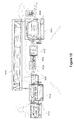
図8は、再構成可能ベクトルプロセッサが使用可能なシステムをブロック図で示している。システム800はマイクロプロセッサ802を有し、これはメモリ(図示せず)に格納されている命令を実行することが可能である。前記プロセッサ802は、他のプロセッサまたはマイクロプロセッサの使用が可能であるが、例えばARM(商標)プロセッサであってもよい。前記システムはさらに、前記再構成可能ベクトルプロセッサの命令を受信し、実行するシーケンサー804を含む。前記シーケンサー804は、適切なシーケンス/順序で命令が実行されるように、適切な制御信号を様々なアレイ・プロセッシング・ユニット(array processing units:APU)806、808、810、812に提供する。前記APU 806、808、810、812の各々は、機能において、再構成可能ベクトルプロセッサ200、400、600、700に関して上述したプロセッシングユニットと類似している。各APUは、アレイ・プロセッシング・ユニット(array control processor:ACP)814のプロセッサと、命令を解読し、適切な制御信号を演算ユニット(computational units:CUs)816に提供する制御ユニットとを有する。前記APU806、808、810、812が有するCUs816の各グループは、上述したベクトルユニットのように動作する。各APUは、32CUsを有するとして図示されており、32サイズを有するベクトルユニットを提供する。CUsの各グループは、組み合わされて、ACPに提供された単一の制御ユニットにより制御可能であり、そして、異なるサイズ、例えば32、64、96、および128のベクトルの処理を提供可能である。
FIG. 8 shows in block diagram a system in which the reconfigurable vector processor can be used.
前記プロセッサ802は、前記APU806、808、810、812によって実行されるシーケンサー804に命令を提供することが可能である。例えば、前記プロセッサ802は、4つの異なるそれぞれのベクトル(各サイズ32)の4つの異なる命令を実行するため前記シーケンサー804に命令を提供することができる。或いは、前記プロセッサ802は、サイズ128の単一ベクトルの1つの命令と、3つの異なるスカラーの3つの異なる命令とを実行する命令を提供することも可能である。
The
上述したように、前記システム800は、リソースを処理する効果的な分配を提供する処理が可能なベクトルサイズを再構成することが可能である。APUsのそれぞれのCUsが異なるAPUによって制御されるようにAUPsが再構成されるとき、前記ACPsにより提供されるスカラーユニットは、1若しくはそれ以上のスカラーの処理を提供するように使用することが可能である。
As described above, the
図9は、再構成可能なベクトルプロセッサを使用するシステムの様々なコンポーネントに接続するAPUをブロック図で示している。APU902は、システム800のAPU806、808、810、812のうちの1つとして使用される。前記APU902は、AXI(advanced extensible interface)バス904に接続され、これにより前記APUの、前記AXIバス904に接続されるシステムの他のコンポーネントとのデータ転送のやりとりを可能にする。AXIバスとして説明されているが、前記APUの、他のコンポーネントとデータ転送のやりとりをする可能にする他のあらゆるタイプのバスまたは接続の使用が可能である。前記APUはまた、データをベクトルデータメモリ(vector data memory:CMEM)にロードするダイレクト・メモリ・アクセスを提供するDMAインターフェース906との接続が可能である。前記ACI904およびDMA906の両方は、前記APUのメモリ空間(図10の1004、1006、および図11の1118)にロードすることが可能である。前記APU902(またはより具体的にはシステム800のシーケンサー804)はまた、当該APU902への信号を妨げるおよび/または制御するシーケンサー910(例えば、システム800のシーケンサー804)に結合されることが可能である。
FIG. 9 illustrates in block diagram an APU that connects to various components of a system that uses a reconfigurable vector processor.
上述されたAXI904およびDMA906接続に加えて、APU902はまた、インターフェース(CMEM_IF)912を介して前記AXIおよびCMEM_DMAに接続され、前記APU902へのデータのロードの出し入れが可能である。前記CMEM_IF 912は、データをベクトル化させ、当該ベクトル化データを前記APU902の」CUs914に提供することが可能である。前記CMEM_IF 912はまた、前AUにスカラーデータを提供することが可能である。前記CMEM_IF 912はまた、前記APU902から前記AXI904または前記CMEM_DMA 912にベクトルデータおよびスカラーデータを提供することが可能である。前記CMEM_IF 912はまた、前記APU(または当該APUに関連するメモリ(CMEM))に新規データをロードし、当該APUが現在データを処理している間古いデータ(または処理済みデータを)取り出すことが可能である。
In addition to the
図10は、ACPのコンポーネントをブロック図で示している。前記ACP1002は、図8の複数のACP806、808、810、812、または図9の908として使用可能である。前記ACP1002は、命令用メモリ(Imem)1004と、データ用メモリ(Dmem)1006とを含む。前記Imem1004および前記Dmem1006は、ホストインターフェース(Host_IF)1008から処理される命令またはデータのいずれかの受信が可能である。前記ホストインターフェース1006は、AXIバスおよび1若しくはそれ以上のDMAチャンネルに接続可能である。前記ACP1002はまた、スカラー・プロセッシング・ユニット1010を含むことが可能である。前記スカラー・プロセッシング・ユニット1010は、1若しくはそれ以上の命令または制御信号(例えば、命令コード、メモリアドレス、シーケンサーからの信号、またはグローバル信号)を受信する。前記スカラー・プロセッシング・ユニット1010は、信号および制御信号を解読し、当該制御信号を他のコンポーネント(例えば、1若しくはそれ以上のベクトルユニット)に提供することが可能である。
FIG. 10 shows the ACP components in a block diagram. The
命令を解読して、制御信号を1若しくはそれ以上のベクトルユニットに提供することに加えて、前記スカラー・プロセッシング・ユニット1010はまた、スカラーを処理するためのコンポーネントを含む。前記スカラープロセッシングコンポーネントは、例えば1若しくはそれ以上のスカラーの加算などの算術関数を実行する例えば算術論理演算装置(arithmetic and logic unit:ALU)1012を含む。前記スカラー・プロセッシング・ユニット1010はまた、1つのスカラーのビットを左または右にシフトするシフトコンポーネント1014と、スカラーを乗算する乗算コンポーネント1016と、実行される図偽の命令のアドレスを生成するアドレス生成ユニット(address generation unit:AGU)とを含む。
In addition to decoding instructions and providing control signals to one or more vector units, the
図11は、CUのコンポーネントをブロック図で示している。CU1102は、複数のCU816、914として使用されることが可能である。前記CU1102は、1つのレジスタ1104と、2つのバイパスマルチプレクサ1106、1108とを含む。理解されているように、前記バイパスマルチプレクサにより、処理パイプラインでの異なる段階からのデータがプロセッサ機能ユニット1110、1112、1114、および1116への入力として使用される。
FIG. 11 shows the components of the CU in a block diagram. The
前記CUは、1若しくはそれ以上のベクトル要素に算術関数を実行するALUユニット1110と、ベクトル要素を乗算する乗算コンポーネント1112と、メモリ1118に結合し、データをロードしたり格納したりするロード/格納ユニット1114とを含む、命令を実行するための様々なコンポーネントを含む。前記CU1102はまた、移動/シフトコンポーネント1116を含む。前記移動/シフトコンポーネント1116は、複数のCU間のデータの移動またはシフトを行う。前記移動/シフトコンポーネント1116は、他の複数のCUの移動/シフトコンポーネントと接続している。異なるプロセッシングユニットのベクトルユニットが一緒に結合して単一のプロセッシングユニットを形成している場合、前記ベクトルユニットの最後の複数のCUの移動/シフトユニットは、1若しくはそれ以上のデータマルチプレクサを介して前記ベクトルユニットの最初の複数のCUの移動/シフトコンポーネントと結合される。
The CU is coupled to an
図11に図示されていないが、CU間に再構成可能な接続を提供することが可能である。例えば、ベクトルユニットは、128x16ビットであってもよい。前記CU間のCU接続は再構成され、例えば64x32ビット、または256x8ビットを提供することが可能である。再構成ベクトルユニットならびに再構成可能なベクトルユニットの利用可能なシステムを説明した。上述の再構成可能ベクトルユニットおよびシステムは、データ処理に必要とされる様々な用途において使用される。例えば、前記再構成可能ベクトルユニットおよびシステムは、音声データ、ビデオデータ、または音声およびビデオデータの両方を処理するのに使用される。 Although not shown in FIG. 11, it is possible to provide a reconfigurable connection between CUs. For example, the vector unit may be 128 × 16 bits. The CU connection between the CUs can be reconfigured to provide, for example, 64 × 32 bits, or 256 × 8 bits. An available system of reconfigurable vector units as well as reconfigurable vector units is described. The reconfigurable vector unit and system described above are used in various applications required for data processing. For example, the reconfigurable vector unit and system is used to process audio data, video data, or both audio and video data.
上述の記載において、再構成可能ベクトルユニットの様々な実施形態を説明してきたが、他の変形も可能である。例えば、再構成可能ベクトルユニットは、複数のプロセッシングユニットから構成され、各々は他のプロセッシングユニットのベクトルユニットを制御することが可能である。 In the above description, various embodiments of reconfigurable vector units have been described, but other variations are possible. For example, the reconfigurable vector unit is composed of a plurality of processing units, each of which can control a vector unit of another processing unit.
図12Aは、上述したように、各プロセッシングユニットが他のプロセッシングユニットのベクトルユニット制御が可能でる場合、当該プロセッシングユニットの各々が制御可能なベクトルサイズを図示している。図示された4つのプロセッシングユニットの各々は、サイズ32、64、96、または128のベクトルユニットの制御が可能である。ベクトルユニットを表す各ブロックの陰影は、どのプロセッシングユニットがそれぞれのベクトルユニットを制御するプロセッシングユニットを制御するのかを図示している。
As described above, FIG. 12A illustrates a vector size that can be controlled by each processing unit when each processing unit can control the vector unit of another processing unit. Each of the four processing units shown is capable of controlling vector units of
プログラミングの柔軟性は、プロセッシングユニットのサブセットのみに他のプロセッシングユニットのベクトルユニットを制御させるようにすることによって減少する。 Programming flexibility is reduced by having only a subset of processing units control the vector units of other processing units.
図12Bは、上述したように、プロセッシングユニット0および2のみが他のプロセッシングユニットのベクトルユニットの制御が可能である場合の、プロセッシングユニットの各々が制御可能であるベクトルサイズを図示している。ベクトルユニットを表す各ブロックの陰影は、どのプロセッシングユニットがそれぞれのベクトルユニットを制御するプロセッシングユニットを制御するのかを図示している。
FIG. 12B illustrates the vector sizes that each of the processing units can control when only processing
図13は、再構成可能ベクトルプロセッサ1300をブロック図で図示している。前記ベクトルプロセッサ1300は、複数のプロセッシングユニット1310、1320、1330、1340を有する。各プロセッシングユニットは、上述したプロセッシングユニット210、220、230、240と類似しており、各々は、スカラーユニット202と、ベクトルユニット204と、制御ユニット206とを有する。しかしながら、ベクトル制御マルチプレクサ208の代わりに、前記再構成可能ベクトルプロセッサは、クロスバースイッチ1302を有する。
FIG. 13 illustrates a
前記クロスバースイッチ1302により、プロセッシングユニットの任意の制御ユニットが別のプロセッシングユニットの任意のベクトルユニットの制御を可能にする。この方法の1つの有意な利点は、ベクトルユニット配分のパイプライン制御が、データの移動を必要とせずに、異なるプロセッシングユニットを介して可能であることである。
The
図14は、サイズ32のベクトルユニットのための24可能ベクトルユニット制御コンフィギュレーションのサブセットを図示している。図14はサイズ32のベクトルユニットの制御のみを図示しているが、上述したように各種サイズの異なるベクトルユニットを制御するとき、クロスバースイッチも使用することが可能であることを理解されたい。プロセッシングユニットは、異なるサイズのベクトルユニット(例えば、64、96、または128)を制御することが可能である。クロスバースイッチ1302のデータパスのルーティング空間を減少させるため、一緒にグループ化され、かつ単一のプロセッシングユニットによって制御されることが可能なベクトルユニットは互いに隣接して配置が可能である。
FIG. 14 illustrates a subset of the 24 possible vector unit control configurations for a
図15は、上述した再構成可能ベクトルプロセッサおよびシステムを使用して処理することが可能な例示的な画像を図示している。図15に関連して記載された用途は、自動車に搭載されたビデオカメラが捕えられたビデオフレームのリアルタイム処理を提供している。ビデオフレームは処理されて、前記フレーム画像の要素を検索し、特定することが可能である。例えば、前記フレーム画像は処理されて、車、道路標識を特定する、ならびに例えば車の死角の検知、または前記フレーム画像の幾何歪み補正(dewarping)などの追加の機能を実行することが可能である。 FIG. 15 illustrates an exemplary image that can be processed using the reconfigurable vector processor and system described above. The application described in connection with FIG. 15 provides real-time processing of video frames captured by a video camera mounted on an automobile. Video frames can be processed to retrieve and identify elements of the frame image. For example, the frame image can be processed to identify cars, road signs, and perform additional functions such as detection of vehicle blind spots, or geometrical dewarping of the frame image, for example. .
全体の画像が最初に処理されて、当該画像の候補要素を検索することができる。前記候補要素は、例えば画像の中の自動車を含む。この処理は、図15のボックス1502、1504、1506、1508、1510、1512、1514として図示されている1若しくはそれ以上の候補要素を特定する。前記候補要素は、道路標識を別処理により検出することも可能であるが、例えば道路標識1516、1518などの対象物を含むことが可能である。全体画像の処理がデータの大部分の処理量を要求するので、画像データの候補検索または処理機能を実行するとき、画像データを処理するのに使用される前記再構成可能ベクトルプロセッサは、最大可能ベクトルサイズを提供するように設定してもよい。再構成可能ベクトルユニットが最大ベクトルサイズを提供するように構成されるとき、3つのスカラーユニットが使用可能である。前記候補検索を実行して、追加機能を提供するときに、これらのスカラーユニットの使用が可能である。この追加機能は、例えば画像を撮るのに使用された魚眼レンズの画像修正のための幾何歪み補正(dewarping)または車の死角にある対象物の検出などを含むことが可能である。
The entire image can be processed first to search for candidate elements of the image. The candidate element includes, for example, a car in the image. This process identifies one or more candidate elements illustrated as
画像が処理され候補要素が特定されると、個々の候補要素(例えば、図15に図示されるボックス1502、1504、1506、1508、1510、1512、1514、1516、1518)は処理され、当該個々の候補要素を検証し、分類することが可能である。それぞれ個々の候補要素のサイズは全体画像のサイズよりも小さいので、最大可能ベクトルサイズを使用する必要はない。このように、再構成可能ベクトルプロセッサは、同じサイズの2つのベクトルユニットを提供するように構成可能である。各ベクトルユニットは、異なる機能に使用可能である。例えば、前記ベクトルユニットのうちの第1のものは、要素を検証し、分類するのに使用することが可能であり、一方第2のベクトルユニットは道路標識のフレーム画像の一部を検索し、または更に特定信号を処理するのに使用することが可能である。
When the image is processed and candidate elements are identified, individual candidate elements (eg,
上述したように、再構成可能ベクトルプロセッサを有するシステムにより、複数のアルゴリズムが当該システムによって実行可能になる。有利な点は、再構成可能ベクトルプロセッサにより、システムが、処理されるアルゴリズムの要求に基づいて効果的な処理を提供するように構成可能であることである。 As described above, a system having a reconfigurable vector processor allows multiple algorithms to be executed by the system. An advantage is that the reconfigurable vector processor allows the system to be configured to provide effective processing based on the requirements of the algorithm being processed.
図16は、再構成可能ベクトルプロセッサによりデータを処理する方法を流れ図で図示している。方法1600は、最初に、複数のそれぞれの他の(スレーブまたは外部)プロセッシングユニットの1若しくはそれ以上に関連するCUsを配分することにより、ベクトルプロセッサのベクトルユニットのサイズを設定する(1602)。前記ベクトルユニットのサイズは、単一の制御(マスターまたは内部)プロセッシングユニットを有する複数のベクトルユニットを制御することにより設定されることが可能である。前記設定サイズのベクトルユニットを使用して、1若しくはそれ以上の命令が実行される(1604)。前記プロセッシングユニットは、前記マスターユニットにより制御可能であり、または必要に応じてのみスカラー処理機能を提供することが可能である。前記ベクトルユニットのサイズは、次に再設定されて、異なるサイズのベクトルユニットを提供する(1606)。前記マスタープロセッシングユニットのベクトルユニットに配分された前記CUsは、特定の処理タスクによって要求される際、サイズの増減が起ることがある。前記ベクトルユニットのサイズが再設定されると、1若しくはそれ以上の命令は、該再設定サイズのベクトルユニットを使用して実行される。上述の方法を用いると、ベクトルユニットによる処理が可能なベクトルサイズに修正することが可能である。
FIG. 16 illustrates in flowchart form a method of processing data by a reconfigurable vector processor. The
図17は、再構成可能ベクトルプロセッサのベクトルユニットのサイズを設定する方法を流れ図で図示している。前記再構成可能ベクトルプロセッサによって実行されるのに必要な処理機能のベクトルサイズが決定される(1702)。多重処理機能が同時に要求される場合、各機能に対するベクトルサイズは、前記プロセッサの能力および利用可能なプロセッシングユニットの数を最大化するように決定される。これは、前記再構成可能ベクトルプロセッサの動作時または開始時、制御マイクロプロセッサによって、またはプログラミングで決定された所定の処理条件、若しくは前記再構成可能ベクトルプロセッサの動作に要求されるコードのコンパイル時間に基づいて、動的に実行される。前記ベクトルサイズを達成するように要求される演算ユニット(CUs)の数は、プロセッシングユニットの利用可能な構成および関連するベクトルユニットに基づいて決定される(1704)。決定されたCU配分を提供するのに要求される1若しくはそれ以上の構成は、前記処理機能の1若しくはそれ以上のものに基づいて決定される(1706)。前記構成は、どのプロセッサがマスタープロセッサ、制御プロセッサ、またはスレーブプロセッサとして動作しているか、およびどのベクトルユニットが配分されるかを決定する。前記プロセッシングユニットのベクトルユニットを制御するための制御信号が生成される(1708)。前記制御信号は、制御プロセッサにより動的に決定可能であり、またはコーディングで生成された設定情報(1707)に基づいて、若しくは前記ベクトルプロセッサによって実行される命令またはアルゴリズムに関連する処理条件を定義する所定の配分基準に基づくコンパイル時間に基づいて生成可能である。前記生成された制御信号は、第1のプロセッシングユニットのベクトルユニットならびに第2のプロセッシングユニットのベクトルユニットに提供される(1710)。前記生成された制御信号を両方のベクトルユニットに提供することにより、前記第1のベクトルユニットにより制御される前記ベクトルユニットのサイズは、増加する。前記ベクトルユニットのサイズは、前記適切な生成された制御信号を例えばベクトル制御マルチプレクサ、データマルチプレクサ、またはデータスイッチなどの再構成可能ベクトルプロセッサの異なるコンポーネントに提供することにより設定または再設定されることが可能である。前記第2のプロセッシングユニットへの制御信号は、当該第2のプロセッシングユニットのスカラー処理リソースを配分して(1712)、当該第2のプロセッシングユニットのスカラー機能を使用してベクトルユニットなしで処理機能を実行し、または当該第2のプロセッシングユニットを前記マスタープロセッシングユニットへのスレーブ処理機能として利用することが可能である。前記第1または第2のサイズのベクトルユニットを使用して命令を実行することに加えて、前記方法はまた、1若しくはそれ以上のスカラープロセッサ、または1若しくはそれ以上の追加ベクトルユニットを使用して命令を実行することが可能である。 FIG. 17 illustrates in flowchart form a method for setting the size of a vector unit of a reconfigurable vector processor. A vector size of processing functions required to be executed by the reconfigurable vector processor is determined (1702). If multiple processing functions are required simultaneously, the vector size for each function is determined to maximize the capacity of the processor and the number of available processing units. This is at the time of operation or start of the reconfigurable vector processor, at a predetermined processing condition determined by the control microprocessor or by programming, or at the compilation time of code required for operation of the reconfigurable vector processor. Based on the dynamic execution. The number of computing units (CUs) required to achieve the vector size is determined based on the available configuration of processing units and the associated vector units (1704). One or more configurations required to provide the determined CU allocation are determined based on one or more of the processing functions (1706). The configuration determines which processors are operating as master processors, control processors, or slave processors, and which vector units are allocated. A control signal for controlling the vector unit of the processing unit is generated (1708). The control signal can be determined dynamically by a control processor or defines processing conditions associated with instructions or algorithms executed by the vector processor based on configuration information (1707) generated by coding or by the vector processor It can be generated based on a compile time based on a predetermined distribution criterion. The generated control signal is provided to the vector unit of the first processing unit as well as the vector unit of the second processing unit (1710). By providing the generated control signal to both vector units, the size of the vector unit controlled by the first vector unit is increased. The size of the vector unit may be set or reset by providing the appropriate generated control signal to different components of a reconfigurable vector processor, such as a vector control multiplexer, data multiplexer, or data switch. Is possible. The control signal to the second processing unit allocates the scalar processing resource of the second processing unit (1712) and uses the scalar function of the second processing unit to perform the processing function without the vector unit. It is possible to execute or use the second processing unit as a slave processing function to the master processing unit. In addition to executing instructions using the first or second sized vector units, the method also uses one or more scalar processors, or one or more additional vector units. It is possible to execute an instruction.
記載の実施形態からの特定の変更および修正を行うことは可能である。従って、上記で議論された実施形態は例示的なものであり、限定するものと解釈されるものではない。 Certain changes and modifications can be made from the described embodiments. Accordingly, the embodiments discussed above are exemplary and are not to be construed as limiting.
Claims (25)
複数のプロセッサユニットであって、各プロセッサユニットは、
スカラーデータの命令を処理するスカラーユニットと、
ベクトルデータの命令を処理するベクトルユニットと、
命令を解読し且つ制御信号を生成して前記スカラーユニット及び前記ベクトルユニットを制御する制御ユニットと
を有する前記複数のプロセッサユニットと、
ベクトル制御セレクタであって、前記複数のプロセッサユニットのうちの1つのプロセッサユニットの1つの前記制御ユニットにより生成された制御信号を、前記複数のプロセッサユニットのうち前記1つのプロセッサユニットとは異なる他のプロセッサユニットに関連したベクトルユニットに選択的に提供して、前記ベクトルユニットが異なる制御ユニットに関連付けられるようにその関連性を変化させるものである、前記ベクトル制御セレクタと
を有する再構成可能プロセッサ。 A reconfigurable processor,
A plurality of processor units, each processor unit comprising:
A scalar unit that processes scalar data instructions;
A vector unit for processing vector data instructions;
A plurality of processor units comprising: a control unit that decodes instructions and generates control signals to control the scalar unit and the vector unit;
A vector control selector, wherein a control signal generated by one control unit of one of the plurality of processor units is different from the one of the plurality of processor units. A reconfigurable processor comprising: a vector control selector that selectively provides to a vector unit associated with a processor unit to change its association such that the vector unit is associated with a different control unit.
データレジスタと、
前記データレジスタに結合された複数のバイパスマルチプレクサと、
前記複数のバイパスマルチプレクサの出力に結合される算術論理演算ユニットと、
前記複数のバイパスマルチプレクサの出力に結合される乗算ユニットと、
前記複数のバイパスマルチプレクサの出力およびメモリに結合されるロード/格納ユニットと、
前記複数のバイパスマルチプレクサの出力および1若しくはそれ以上の他の演算ユニットに結合される移動/シフトユニットと
を有するものである、再構成可能プロセッサ。 The reconfigurable processor of claim 13, wherein each CU is
A data register;
A plurality of bypass multiplexers coupled to the data register;
An arithmetic logic unit coupled to the outputs of the plurality of bypass multiplexers;
A multiplication unit coupled to the outputs of the plurality of bypass multiplexers;
A load / store unit coupled to the output and memory of the plurality of bypass multiplexers;
A reconfigurable processor having a plurality of bypass multiplexer outputs and a move / shift unit coupled to one or more other arithmetic units.
第1のサイズのベクトルアレイを提供して前記第1のサイズのデータを処理するように前記複数のプロセッサユニットのうちの1つのプロセッサユニットを設定する工程であって、前記ベクトルアレイは、前記複数のプロセッサユニットのうちの異なるプロセッサユニットに関連したベクトルユニットを前記1つのプロセッサユニットに選択的に関連付けることにより提供されるものである、前記設定する工程と、
前記第1のサイズのベクトルアレイを使用して1若しくはそれ以上の命令を実行し、前記第1のサイズのデータを処理する工程と、
前記ベクトルアレイを第2のサイズに変化させて前記第2のサイズのデータを処理するように前記複数のプロセッサユニットのうちの1つのプロセッサユニットを再設定する工程であって、この工程は、前記複数のプロセッサユニットのうちの異なるプロセッサユニットに関連したベクトルユニットを前記1つのプロセッサユニットに関連付けるようにその関連性を選択的に変化させることにより前記1つのプロセッサユニットを再設定するものである、前記再設定する工程と、
前記第2のサイズのベクトルアレイを使用して1若しくはそれ以上の命令を実行し、前記第2のサイズのデータを処理する工程と
を有する方法。 A method of processing data using a reconfigurable processor, comprising a plurality of processor units,
Configuring a processor unit of the plurality of processor units to provide a first size vector array to process the first size data, the vector array comprising the plurality of The setting step, provided by selectively associating a vector unit associated with a different one of the processor units with the one processor unit;
Executing one or more instructions using the first size vector array to process the first size data;
Reconfiguring one of the plurality of processor units to change the vector array to a second size and process data of the second size, the step comprising: Reconfiguring the one processor unit by selectively changing its association to associate a vector unit associated with a different processor unit of the plurality of processor units with the one processor unit; A resetting process;
Executing one or more instructions using the second size vector array to process the second size data.
前記プロセッサユニットを設定および再設定する工程は、
前記複数のプロセッサユニットのうちの第1のプロセッサユニットのベクトルユニットを制御する制御信号を生成する工程と、
前記生成された制御信号を前記第1のプロセッサユニットのベクトルユニットと第2のプロセッサユニットのベクトルユニットとに提供して、前記第1および第2のプロセッサユニットの個別のベクトルユニットの合計の総サイズをベクトルアレイに提供する工程と
を有するものである、方法。 The method of claim 17, wherein
The step of setting and resetting the processor unit includes:
Generating a control signal for controlling a vector unit of a first processor unit of the plurality of processor units;
Providing the generated control signal to a vector unit of the first processor unit and a vector unit of the second processor unit, so that a total total size of the individual vector units of the first and second processor units; Providing to a vector array.
スカラーデータの命令を処理するスカラーユニットと、
ベクトルデータの命令を処理するベクトルユニットと、
命令を解読し且つ制御信号を生成して前記スカラーユニット及び前記ベクトルユニットを制御する制御ユニットと
を有するものである、方法。 20. The method according to any one of claims 17 to 19, wherein each of the plurality of processor units is
A scalar unit that processes scalar data instructions;
A vector unit for processing vector data instructions;
A control unit that decodes instructions and generates control signals to control the scalar unit and the vector unit.
データレジスタと、
前記データレジスタに結合された複数のバイパスマルチプレクサと、
前記複数のバイパスマルチプレクサの出力に結合される算術論理演算ユニットと、
前記複数のバイパスマルチプレクサの出力に結合される乗算ユニットと、
前記複数のバイパスマルチプレクサの出力およびメモリに結合されるロード/格納ユニットと、
前記複数のバイパスマルチプレクサの出力および1若しくはそれ以上の他の演算ユニットに結合される移動/シフトユニットと
を有するものである、方法。 24. The method of claim 23, wherein each CU is
A data register;
A plurality of bypass multiplexers coupled to the data register;
An arithmetic logic unit coupled to the outputs of the plurality of bypass multiplexers;
A multiplication unit coupled to the outputs of the plurality of bypass multiplexers;
A load / store unit coupled to the output and memory of the plurality of bypass multiplexers;
A shift / shift unit coupled to the outputs of the plurality of bypass multiplexers and one or more other arithmetic units.
Applications Claiming Priority (1)
| Application Number | Priority Date | Filing Date | Title |
|---|---|---|---|
| PCT/CA2011/000080 WO2012100316A1 (en) | 2011-01-25 | 2011-01-25 | Apparatus and method of vector unit sharing |
Publications (3)
| Publication Number | Publication Date |
|---|---|
| JP2014509419A JP2014509419A (en) | 2014-04-17 |
| JP2014509419A5 JP2014509419A5 (en) | 2015-08-20 |
| JP5971635B2 true JP5971635B2 (en) | 2016-08-17 |
Family
ID=46580137
Family Applications (1)
| Application Number | Title | Priority Date | Filing Date |
|---|---|---|---|
| JP2013550709A Active JP5971635B2 (en) | 2011-01-25 | 2011-01-25 | Vector unit sharing apparatus and method |
Country Status (5)
| Country | Link |
|---|---|
| US (1) | US9727526B2 (en) |
| JP (1) | JP5971635B2 (en) |
| CA (1) | CA2859999A1 (en) |
| DE (1) | DE112011104770B4 (en) |
| WO (1) | WO2012100316A1 (en) |
Families Citing this family (6)
| Publication number | Priority date | Publication date | Assignee | Title |
|---|---|---|---|---|
| US9292569B2 (en) * | 2012-10-02 | 2016-03-22 | Oracle International Corporation | Semi-join acceleration |
| JP6102528B2 (en) * | 2013-06-03 | 2017-03-29 | 富士通株式会社 | Signal processing apparatus and signal processing method |
| KR102332523B1 (en) * | 2014-12-24 | 2021-11-29 | 삼성전자주식회사 | Apparatus and method for execution processing |
| CN105335130B (en) * | 2015-09-28 | 2018-06-26 | 深圳市中兴微电子技术有限公司 | A kind of processor and its method for handling task |
| US10620957B2 (en) | 2015-10-22 | 2020-04-14 | Texas Instruments Incorporated | Method for forming constant extensions in the same execute packet in a VLIW processor |
| US10241946B2 (en) | 2017-01-18 | 2019-03-26 | Nxp Usa, Inc. | Multi-channel DMA system with command queue structure supporting three DMA modes |
Family Cites Families (21)
| Publication number | Priority date | Publication date | Assignee | Title |
|---|---|---|---|---|
| JPS58134357A (en) * | 1982-02-03 | 1983-08-10 | Hitachi Ltd | Array processor |
| DE3506749A1 (en) * | 1984-02-27 | 1985-09-26 | Nippon Telegraph & Telephone Public Corp., Tokio/Tokyo | Matrix processor and control method therefor |
| US4771380A (en) * | 1984-06-22 | 1988-09-13 | International Business Machines Corp. | Virtual vector registers for vector processing system |
| US4760525A (en) * | 1986-06-10 | 1988-07-26 | The United States Of America As Represented By The Secretary Of The Air Force | Complex arithmetic vector processor for performing control function, scalar operation, and set-up of vector signal processing instruction |
| US5010477A (en) * | 1986-10-17 | 1991-04-23 | Hitachi, Ltd. | Method and apparatus for transferring vector data between parallel processing system with registers & logic for inter-processor data communication independents of processing operations |
| US5475656A (en) | 1989-09-27 | 1995-12-12 | Hitachi, Ltd. | Optical disk memory and information processing apparatus |
| US5197130A (en) * | 1989-12-29 | 1993-03-23 | Supercomputer Systems Limited Partnership | Cluster architecture for a highly parallel scalar/vector multiprocessor system |
| JPH0520283A (en) * | 1991-07-11 | 1993-01-29 | Mitsubishi Electric Corp | Parallel data processor |
| CA2073516A1 (en) * | 1991-11-27 | 1993-05-28 | Peter Michael Kogge | Dynamic multi-mode parallel processor array architecture computer system |
| JP3639323B2 (en) * | 1994-03-31 | 2005-04-20 | 富士通株式会社 | Simultaneous linear equation calculation processing method and computer using memory distributed parallel computer |
| US5513366A (en) * | 1994-09-28 | 1996-04-30 | International Business Machines Corporation | Method and system for dynamically reconfiguring a register file in a vector processor |
| US6317819B1 (en) * | 1996-01-11 | 2001-11-13 | Steven G. Morton | Digital signal processor containing scalar processor and a plurality of vector processors operating from a single instruction |
| JP3344345B2 (en) | 1998-12-15 | 2002-11-11 | 日本電気株式会社 | Shared memory type vector processing system, control method thereof, and storage medium for storing vector processing control program |
| IL145245A0 (en) * | 2001-09-03 | 2002-06-30 | Jtc 2000 Dev Delaware Inc | System and method including vector-matrix multiplication |
| ATE372542T1 (en) * | 2002-05-24 | 2007-09-15 | Nxp Bv | ACCESS TO WIDE STORAGE |
| CN100541425C (en) * | 2002-05-24 | 2009-09-16 | Nxp股份有限公司 | scalar/vector processor |
| US6986023B2 (en) * | 2002-08-09 | 2006-01-10 | Intel Corporation | Conditional execution of coprocessor instruction based on main processor arithmetic flags |
| US7334110B1 (en) | 2003-08-18 | 2008-02-19 | Cray Inc. | Decoupled scalar/vector computer architecture system and method |
| JP5240424B2 (en) | 2004-11-05 | 2013-07-17 | 日本電気株式会社 | SIMD type parallel processing unit, processing element, control method for SIMD type parallel processing unit |
| US20090150648A1 (en) * | 2007-12-06 | 2009-06-11 | Eric Oliver Mejdrich | Vector Permute and Vector Register File Write Mask Instruction Variant State Extension for RISC Length Vector Instructions |
| US8495342B2 (en) * | 2008-12-16 | 2013-07-23 | International Business Machines Corporation | Configuring plural cores to perform an instruction having a multi-core characteristic |
-
2011
- 2011-01-25 CA CA2859999A patent/CA2859999A1/en not_active Abandoned
- 2011-01-25 DE DE112011104770.3T patent/DE112011104770B4/en active Active
- 2011-01-25 JP JP2013550709A patent/JP5971635B2/en active Active
- 2011-01-25 US US13/981,851 patent/US9727526B2/en active Active
- 2011-01-25 WO PCT/CA2011/000080 patent/WO2012100316A1/en active Application Filing
Also Published As
| Publication number | Publication date |
|---|---|
| WO2012100316A1 (en) | 2012-08-02 |
| DE112011104770T5 (en) | 2013-10-31 |
| CA2859999A1 (en) | 2012-08-02 |
| JP2014509419A (en) | 2014-04-17 |
| US9727526B2 (en) | 2017-08-08 |
| US20140006748A1 (en) | 2014-01-02 |
| DE112011104770B4 (en) | 2022-08-25 |
Similar Documents
| Publication | Publication Date | Title |
|---|---|---|
| JP5971635B2 (en) | Vector unit sharing apparatus and method | |
| US11669330B2 (en) | Method for performing random read access to a block of data using parallel LUT read instruction in vector processors | |
| US11645224B2 (en) | Neural processing accelerator | |
| JP6373991B2 (en) | Vector processing engine utilizing tapped delay line for filter vector processing operations and associated vector processing system and method | |
| US6366998B1 (en) | Reconfigurable functional units for implementing a hybrid VLIW-SIMD programming model | |
| CN107229463B (en) | Computing device and corresponding computing method | |
| JP4624098B2 (en) | Processor address generation unit | |
| EP3069233A1 (en) | Vector processing engine employing reordering circuitry in data flow paths between vector data memory and execution units, and related method | |
| JPH0850575A (en) | Programmable processor,method for execution of digital signal processing by using said programmable processor and its improvement | |
| EP3069234A1 (en) | Vector processing engines employing a tapped-delay line for correlation vector processing operations, and related vector processor systems and methods | |
| CN108319559B (en) | Data processing apparatus and method for controlling vector memory access | |
| US20200265106A1 (en) | Two-dimensional multi-layer convolution for deep learning | |
| US10908916B2 (en) | Apparatus and method for executing a plurality of threads | |
| JP2020508512A (en) | Multiplication and accumulation in data processing equipment | |
| TWI803634B (en) | Processor, method of operating a processor, processing apparatus and non-transitory computer-readable medium comprising instructions of loading and replication of sub-vector values | |
| CN111183418B (en) | Configurable hardware accelerator | |
| JP7245833B2 (en) | Configurable hardware runtime optimizations | |
| US20080209165A1 (en) | Simd microprocessor, image processing apparatus including same, and image processing method used therein | |
| EP4195062A1 (en) | Method and apparatus for separable convolution filter operations on matrix multiplication arrays | |
| US20150254076A1 (en) | Data processing apparatus and method for performing vector scan operation | |
| US7673117B2 (en) | Operation apparatus | |
| US9606798B2 (en) | VLIW processor, instruction structure, and instruction execution method | |
| US20230059970A1 (en) | Weight sparsity in data processing engines | |
| US20060271610A1 (en) | Digital signal processor having reconfigurable data paths | |
| JPH044457A (en) | System for mutually connecting main processor and additional processor |
Legal Events
| Date | Code | Title | Description |
|---|---|---|---|
| A521 | Request for written amendment filed |
Free format text: JAPANESE INTERMEDIATE CODE: A523 Effective date: 20140124 |
|
| A621 | Written request for application examination |
Free format text: JAPANESE INTERMEDIATE CODE: A621 Effective date: 20140124 |
|
| A977 | Report on retrieval |
Free format text: JAPANESE INTERMEDIATE CODE: A971007 Effective date: 20141217 |
|
| A131 | Notification of reasons for refusal |
Free format text: JAPANESE INTERMEDIATE CODE: A131 Effective date: 20150106 |
|
| A601 | Written request for extension of time |
Free format text: JAPANESE INTERMEDIATE CODE: A601 Effective date: 20150404 |
|
| A601 | Written request for extension of time |
Free format text: JAPANESE INTERMEDIATE CODE: A601 Effective date: 20150507 |
|
| A601 | Written request for extension of time |
Free format text: JAPANESE INTERMEDIATE CODE: A601 Effective date: 20150606 |
|
| A521 | Request for written amendment filed |
Free format text: JAPANESE INTERMEDIATE CODE: A523 Effective date: 20150703 |
|
| A524 | Written submission of copy of amendment under article 19 pct |
Free format text: JAPANESE INTERMEDIATE CODE: A524 Effective date: 20150703 |
|
| A131 | Notification of reasons for refusal |
Free format text: JAPANESE INTERMEDIATE CODE: A131 Effective date: 20160202 |
|
| A521 | Request for written amendment filed |
Free format text: JAPANESE INTERMEDIATE CODE: A523 Effective date: 20160502 |
|
| TRDD | Decision of grant or rejection written | ||
| A01 | Written decision to grant a patent or to grant a registration (utility model) |
Free format text: JAPANESE INTERMEDIATE CODE: A01 Effective date: 20160607 |
|
| A711 | Notification of change in applicant |
Free format text: JAPANESE INTERMEDIATE CODE: A712 Effective date: 20160623 |
|
| A61 | First payment of annual fees (during grant procedure) |
Free format text: JAPANESE INTERMEDIATE CODE: A61 Effective date: 20160704 |
|
| A521 | Request for written amendment filed |
Free format text: JAPANESE INTERMEDIATE CODE: A821 Effective date: 20160623 |
|
| R150 | Certificate of patent or registration of utility model |
Ref document number: 5971635 Country of ref document: JP Free format text: JAPANESE INTERMEDIATE CODE: R150 |
|
| R250 | Receipt of annual fees |
Free format text: JAPANESE INTERMEDIATE CODE: R250 |
|
| R250 | Receipt of annual fees |
Free format text: JAPANESE INTERMEDIATE CODE: R250 |
|
| R250 | Receipt of annual fees |
Free format text: JAPANESE INTERMEDIATE CODE: R250 |
|
| R250 | Receipt of annual fees |
Free format text: JAPANESE INTERMEDIATE CODE: R250 |
|
| R250 | Receipt of annual fees |
Free format text: JAPANESE INTERMEDIATE CODE: R250 |