JP5957611B1 - Non-contact input device and method - Google Patents
Non-contact input device and method Download PDFInfo
- Publication number
- JP5957611B1 JP5957611B1 JP2015531364A JP2015531364A JP5957611B1 JP 5957611 B1 JP5957611 B1 JP 5957611B1 JP 2015531364 A JP2015531364 A JP 2015531364A JP 2015531364 A JP2015531364 A JP 2015531364A JP 5957611 B1 JP5957611 B1 JP 5957611B1
- Authority
- JP
- Japan
- Prior art keywords
- light
- display
- image
- infrared
- real image
- Prior art date
- Legal status (The legal status is an assumption and is not a legal conclusion. Google has not performed a legal analysis and makes no representation as to the accuracy of the status listed.)
- Active
Links
Images


Abstract
平面視して交差する第1、第2の微小反射面20、21がそれぞれ同一平面上に多数立設して配置された光結像手段13と、光結像手段13の一側に設けられたディスプレイ11とを有し、ディスプレイ11の画像11aを光結像手段13の他側に第1の実像12として形成し、第1の実像12に触れた指示手段34の画像位置を光学的に検知する非接触入力装置10において、ディスプレイ11の表面に、表側からの光のみを検知するセンサ素子28が並んで設けられた光センサ26を有し、指示手段34からの反射光を光結像手段13を介してディスプレイ11上に第2の実像35として形成し、第2の実像35の位置を光センサ26で検知する。A plurality of first and second micro-reflecting surfaces 20 and 21 intersecting in plan view are arranged on the same plane, and are provided on one side of the light imaging means 13. The image 11a of the display 11 is formed as the first real image 12 on the other side of the optical imaging means 13, and the image position of the pointing means 34 that has touched the first real image 12 is optically determined. In the non-contact input device 10 that detects, the surface of the display 11 has a light sensor 26 provided with a sensor element 28 that detects only light from the front side, and the reflected light from the instruction means 34 is optically imaged. A second real image 35 is formed on the display 11 via the means 13, and the position of the second real image 35 is detected by the optical sensor 26.
Description
本発明は、空中に実像を形成し、この実像(例えば、タッチパネル像)を見ながら指示手段(例えば、指)の操作によって信号入力ができる非接触入力装置及び方法(即ち、再生画像の指示位置を非接触で検知する装置及び方法)に関する。 The present invention relates to a non-contact input device and method that can form a real image in the air and can input a signal by operating an instruction means (for example, a finger) while viewing the real image (for example, a touch panel image) (that is, an indication position of a reproduction image) And non-contact detection apparatus and method).
ディスプレイ(表示器)に画像を表示し、画像の特定の場所を指で押すと感圧センサなどで押圧部分のXY座標が検知され、この入力信号によって次の動作を行うことは従来から知られている(例えば、特許文献1参照)。 It is conventionally known that an image is displayed on a display (display device), and when a specific place of the image is pressed with a finger, the XY coordinates of the pressed portion are detected by a pressure sensor or the like, and the next operation is performed by this input signal. (For example, refer to Patent Document 1).
また、特許文献2に記載されているように、ディスプレイの直上に発光素子と受光素子をXY軸に沿って多数平行に並べてマトリックスを形成し、指やペン等の障害物でディスプレイの表面をタッチした場合は、その障害物がマトリックスを横切ることで、ディスプレイに当接した位置を検知することも提案されている。 Also, as described in Patent Document 2, a matrix is formed by arranging a number of light emitting elements and light receiving elements in parallel along the XY axes directly above the display, and the surface of the display is touched with an obstacle such as a finger or a pen. In such a case, it has been proposed to detect the position where the obstacle is in contact with the display by crossing the matrix.
一方、特許文献3には、透明平板の内部に多数の第1、第2の平面光反射部を平行かつ一定間隔でそれぞれ並べた第1、第2の光制御パネルを、第1、第2の平面光反射部が平面視して直交状態となるように当接又は近接配置した光結像手段を用い、ディスプレイの画像とディスプレイ表面に赤外線を乱反射させた画像とを同時に再生画像として空中に表示し、再生画像にタッチした指示手段の位置を二次元赤外線カメラによって検知して、再生画像の指示位置を検知する方法及び装置が提案されている。 On the other hand, Patent Document 3 discloses first and second light control panels in which a large number of first and second planar light reflecting portions are arranged in parallel and at regular intervals inside a transparent flat plate. Using the optical imaging means placed in contact with or close to each other so that the planar light reflecting portion is in an orthogonal state in plan view, the image on the display and the image on which the infrared rays are irregularly reflected on the display surface are simultaneously reproduced in the air as a reproduced image There has been proposed a method and an apparatus for detecting the position of the reproduction image by detecting the position of the instruction means displayed and touching the reproduction image with a two-dimensional infrared camera.
また、特許文献4に記載されているように、液晶パネルを構成するトランジスタ形状面に光センサを内蔵させ、液晶表面での指によるマルチタッチやタッチペンの動きの形状を認識する装置も提案されている。 Also, as described in Patent Document 4, a device has been proposed in which an optical sensor is built in a transistor shape surface constituting a liquid crystal panel to recognize the shape of multi-touch with a finger on the surface of the liquid crystal or the movement of a touch pen. Yes.
しかしながら、特許文献1、2記載のタッチパネルにおいては、平面状のディスプレイが存在し、ディスプレイに特定の平面画像が表示され、そのディスプレイ上の特定の位置を押圧して入力位置が検知できる構造となっていた。従って、指やペン等で画像を押した場合、必ずディスプレイ面又はタッチパネル面に接触又は衝突し、ディスプレイ等が汚れる又はディスプレイに疵を付けることがあった。 However, the touch panels described in Patent Documents 1 and 2 have a flat display, a specific flat image is displayed on the display, and the input position can be detected by pressing a specific position on the display. It was. Therefore, when an image is pressed with a finger or a pen, the display surface or the touch panel surface is always contacted or collided, and the display or the like may become dirty or the display may be wrinkled.
特許文献3には、ディスプレイの他に赤外線の発生手段(赤外線ライト)、赤外線の乱反射面、及び赤外線カメラも必要となって装置構成がより複雑になる。また、赤外線発生手段、赤外線カメラはディスプレイ及び光結像手段とは別位置に配置されているので、設置空間を必要とするという問題があった。そして、ディスプレイの正面側に赤外線の乱反射面を置くので、ディプレイの光の一部が吸収されるという問題があった。更に、特許文献3においては、光結像手段を用いているのでレンズのように結像のための焦点距離は有さないが、特に、赤外線カメラを使用する場合、設置位置を選定し、更に映像に対する焦点(ピント)調整を行う必要がある。
特許文献4には、バックライト付きの液晶パネルと、液晶パネルにタッチしたことを反射光によって検知する光センサを備えた光学式タッチパネルが提案されているが、タッチパネルは空中結像式ではない。
In Patent Document 3, an infrared generation means (infrared light), an infrared diffuse reflection surface, and an infrared camera are required in addition to the display, and the apparatus configuration becomes more complicated. In addition, since the infrared generation means and the infrared camera are arranged at positions different from the display and the optical imaging means, there is a problem that an installation space is required. In addition, since the infrared diffuse reflection surface is placed on the front side of the display, there is a problem that a part of the light of the display is absorbed. Further, in Patent Document 3, since the optical imaging means is used, there is no focal length for imaging as in the case of a lens. However, particularly when an infrared camera is used, the installation position is selected, and It is necessary to adjust the focus on the image.
Patent Document 4 proposes an optical touch panel including a liquid crystal panel with a backlight and an optical sensor that detects that the liquid crystal panel is touched by reflected light, but the touch panel is not an aerial imaging type.
更に、ATMなどでもディスプレイを用いたタッチパネルは使用されているが、不特定多数の人が画面に触れるので衛生的ではなく、接触感染防止には有効ではなかった。
また、ディスプレイに向けて光が照射されると、その反射光がディスプレイから放射され、ディスプレイが見にくい場合があった。
Furthermore, although a touch panel using a display is also used in ATMs and the like, it is not hygienic because an unspecified number of people touch the screen, and is not effective in preventing contact infection.
Moreover, when light is irradiated toward the display, the reflected light is emitted from the display, and the display may be difficult to see.
本発明はかかる事情に鑑みてなされたもので、結像させる画像を他の光源からの反射光でない空間画像とし、この空間画像の特定位置を指、指示棒、タッチペン等の指示手段で指してその位置を検知し、ディスプレイに物理的に接触しなくても信号入力ができる非接触入力装置及び方法を提供することを目的とする。 The present invention has been made in view of such circumstances, and an image to be formed is a spatial image that is not reflected light from another light source, and a specific position of the spatial image is pointed to by a pointing means such as a finger, a pointing stick, or a touch pen. An object of the present invention is to provide a non-contact input device and method capable of detecting the position and inputting a signal without physically touching the display.
前記目的に沿う本発明に係る非接触入力装置は、平面視して交差する第1、第2の微小反射面がそれぞれ同一平面上に多数立設して配置され、前記各第1の微小反射面からの第1の反射光を、対応する前記第2の微小反射面で受けて第2の反射光とする光結像手段と、該光結像手段の一側に距離をおいて設けられたディスプレイとを有し、前記ディスプレイの画像を前記光結像手段の他側に第1の実像として形成し、該第1の実像に触れた指示手段の画像位置を光学的に検知する非接触入力装置において、
前記光結像手段の他側に、前記第1の実像が形成される範囲を照らす赤外線の照明器が設けられ、前記ディスプレイの表面に、表側からの赤外光のみを検知する赤外線センサ素子が並んで設けられたシート状の光センサが設けられ、前記指示手段からの赤外線(赤外光と称することもある)の反射光を前記光結像手段を介して前記ディスプレイ上に第2の実像として形成し、該第2の実像の位置を前記光センサで検知する。
In the non-contact input device according to the present invention that meets the object, a plurality of first and second micro-reflecting surfaces intersecting each other in plan view are arranged on the same plane, and each of the first micro-reflections is arranged. An optical imaging means for receiving the first reflected light from the surface by the corresponding second micro-reflecting surface and making the second reflected light; and a distance on one side of the optical imaging means. A non-contact type image forming apparatus configured to form an image of the display as a first real image on the other side of the optical imaging unit and optically detecting an image position of the pointing unit that has touched the first real image. In the input device,
On the other side of the optical imaging means, the infrared illuminators is provided a first real image shines range formed on the surface of the display, the infrared sensor device that detects only the infrared light from the front side lined provided sheet-shaped optical sensor provided, the second real image light reflected on said display through the optical imaging means of an infrared (sometimes referred to as infrared light) from the instruction unit And the position of the second real image is detected by the optical sensor.
本発明に係る非接触入力装置において、前記ディスプレイから発する光の一部又は全部は高周波変調(例えば、数kHz〜200MHz)されているのが好ましい。
また、前記ディスプレイから発する光は赤外線を含み、前記各センサ素子は赤外線センサ素子であるのが好ましい。
In the non-contact input device according to the present invention, it is preferable that a part or all of the light emitted from the display is high-frequency modulated (for example, several kHz to 200 MHz).
Moreover, it is preferable that the light emitted from the display includes an infrared ray, and each sensor element is an infrared sensor element.
そして、本発明に係る非接触入力装置において、前記各センサ素子は、裏側に非透光材が設けられているのが好ましい。前記センサ素子が可視光の光センサ素子である場合は、可視光を遮断する非透光材を、前記センサ素子が赤外線センサ素子である場合は、赤外線を遮断する非透光材を使用する。 And in the non-contact input device which concerns on this invention, it is preferable that the said each sensor element is provided with the non-light-transmissive material in the back side. When the sensor element is a visible light sensor element, a non-translucent material that blocks visible light is used. When the sensor element is an infrared sensor element, a non-translucent material that blocks infrared light is used.
また、前記目的に沿う本発明に係る非接触入力方法は、平面視して交差する第1、第2の微小反射面がそれぞれ同一平面上に多数立設して配置され、前記各第1の微小反射面からの第1の反射光を、対応する前記第2の微小反射面で受けて第2の反射光とする光結像手段と、該光結像手段の一側に距離をおいて設けられたディスプレイとを用い、前記ディスプレイの画像を前記光結像手段の他側に第1の実像として形成し、該第1の実像に触れた指示手段の画像位置を光学的に検知する非接触入力方法において、
前記光結像手段の他側に、前記第1の実像が形成される範囲を照らす赤外線の照明器を設け、前記ディスプレイの表面に、表側からの赤外光を検知する赤外線センサ素子が並んで設けられたシート状の光センサを設け、赤外光が照射され、前記第1の実像に触れた前記指示手段の画像を、前記光結像手段を介して前記ディスプレイの表面に第2の実像として形成し、赤外光を検知する前記光センサで前記第2の実像の位置を検知する。
In the non-contact input method according to the present invention that meets the object, a plurality of first and second micro-reflecting surfaces intersecting each other in plan view are arranged on the same plane, The first reflected light from the minute reflecting surface is received by the corresponding second minute reflecting surface to be the second reflected light, and a distance is provided on one side of the light imaging means. The display is provided, and an image on the display is formed as a first real image on the other side of the optical imaging unit, and an image position of the pointing unit that touches the first real image is optically detected. In the contact input method,
On the other side of the optical imaging means, the illuminator infrared illuminating range of the first real image is formed is provided, on the surface of the display, side by side infrared sensor elements for detecting the infrared light from the front side A sheet-like optical sensor is provided, and an image of the pointing means that is irradiated with infrared light and touches the first real image is displayed on the surface of the display via the light imaging means. And the position of the second real image is detected by the optical sensor that detects infrared light .
そして、本発明に係る非接触入力方法において、前記ディスプレイから発する光は赤外線を含み、前記各センサ素子は赤外線センサ素子であるのが好ましい。 In the non-contact input method according to the present invention, it is preferable that the light emitted from the display includes infrared rays, and each of the sensor elements is an infrared sensor element.
本発明に係る非接触入力装置及び非接触入力方法は、ディスプレイの表面に、表側からの赤外光のみを検知するセンサ素子が並んで設けられた光センサを有し、指示手段からの反射光を光結像手段を介してディスプレイ上に第2の実像として形成し、第2の実像の位置を光センサで検知するので、特別な赤外線発生手段や赤外線カメラ等を備えることなく、比較的簡単に、指示手段の位置を検出できる。
また、光結像手段はレンズ(カメラ)と異なり、特別な焦点距離を有さないので、ディスプレイの位置が変わっても、指示手段の画像は元のディスプレイ上に結像し、より正確な指示手段(例えば、指、ペン先等)の位置の検出ができる。
A non-contact input device and a non-contact input method according to the present invention include a photosensor in which sensor elements that detect only infrared light from the front side are arranged on the surface of a display, and reflected light from an instruction unit. Is formed as a second real image on the display via the optical image forming means, and the position of the second real image is detected by the optical sensor, so that it is relatively simple without providing a special infrared ray generating means or an infrared camera. In addition, the position of the pointing means can be detected.
In addition, unlike the lens (camera), the optical imaging means does not have a special focal length, so even if the display position changes, the image on the indication means is imaged on the original display, giving a more accurate indication. The position of the means (for example, finger, pen tip, etc.) can be detected.
特に、本発明に係る非接触入力装置及び非接触入力方法において、ディスプレイから発する光が赤外線を含み、光センサのセンサ素子が赤外線センサ素子である場合は、目視できない赤外線によって、指示手段の位置を検知できる。
また、本発明に係る非接触入力装置において、光センサがシート状に形成される場合、光センサを有するディスプレイの製造が容易となり、通常のディスプレイの採用も可能となる。更に、光として可視光を使用する場合は、従来の「光センサ液晶パッド」をそのままディスプレイに利用できる。この場合は、センサ素子は裏側に非透光材を配置して、表側からの光のみを検知するようにするのがよい。なお、光センサをシート状としてディスプレイ上に載せる場合は、ディスプレイとは別構造のものであってもよい。
シート状の光センサで受光した第2の実像は、各センサ素子の受光データから重心位置を探す等の演算処理を行って指示手段(例えば、指先)の位置を求める。
In particular, in the non-contact input device and the non-contact input method according to the present invention, when the light emitted from the display includes infrared rays and the sensor element of the optical sensor is an infrared sensor element, the position of the indication means is determined by infrared rays that are not visible. Can be detected.
Further, in the non-contact input device according to the present invention, when the optical sensor is formed in a sheet shape, it is easy to manufacture a display having the optical sensor, and a normal display can be adopted. Further, when using visible light as light, a conventional “photosensor liquid crystal pad” can be used as it is for a display. In this case, the sensor element is preferably provided with a non-light-transmitting material on the back side so as to detect only light from the front side. In addition, when mounting an optical sensor on a display as a sheet form, the thing of a structure different from a display may be sufficient.
The second real image received by the sheet-like optical sensor is subjected to arithmetic processing such as searching for the position of the center of gravity from the light reception data of each sensor element to obtain the position of the pointing means (for example, fingertip).
ここで、ディスプレイの画像をキーボート等にする場合は、特別な光線画像(例えば、スポットライト)を個々のキーボードの中心に設けるのが好ましい。これによって、光センサの位置も光線画像に合わせて、検知精度を向上することができる。 Here, when the display image is a keyboard or the like, it is preferable to provide a special light image (for example, a spotlight) at the center of each keyboard. Accordingly, the detection accuracy can be improved by matching the position of the optical sensor with the light image.
続いて、添付した図面を参照しながら、本発明を具体化した実施例について説明する。
図1に示すように、本発明の一実施例に係る非接触入力装置10は、平面状のディスプレイ11と、このディスプレイ11と例えば30〜60度の角度αを有して離れて形成され、ディスプレイ11に表示される画像11a(図2参照)を入光して対称位置にディスプレイ11の画像11aを第1の実像12として結像する光結像手段13を備えている。なお、ここで、ディスプレイとしては通常の液晶ディスプレイのように平面板状のものの他に、内部に光源を有する立体状のもの、キーボードのように片側にのみ凹凸を有するものを使用することもできるし、場合によっては、内部に光源(バックライト)を有する看板(電光表示器等の静止画表示器)のようなものも使用できる。特に、静止画は立体又は平面状のものであってもよい。
Next, embodiments of the present invention will be described with reference to the accompanying drawings.
As shown in FIG. 1, a
また、光結像手段13が透明プラスチック、ガラス等の透明材を主要材料として使用している場合は、空気中から透明材に入光し、透明材から空気中に出光するときに、透明材の材質に起因する屈折を生じるので、屈折角を考慮してディスプレイ11の位置を決める。なお、光結像手段に対するディスプレイの位置はある程度自由であり、レンズ系を用いる場合のピント合わせは必要でない。
Further, when the light imaging means 13 uses a transparent material such as transparent plastic or glass as a main material, the transparent material enters the transparent material from the air and emits the light from the transparent material into the air. Since the refraction caused by the material is generated, the position of the
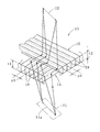
光結像手段13は、図2に詳細を示すように、一面側を当接又は近接して配置されたそれぞれ厚みがt1、t2(例えば、0.1〜5mm)の平板状の第1、第2の光制御パネル14、15を有している。第1、第2の光制御パネル14、15内部には、それぞれ一方側の面に垂直に多数かつ帯状の平面光反射部18、19が一定のピッチ(p1、p2)で多数並べて形成されている。ここで、第1、第2の光制御パネル14、15の立設する平面光反射部18、19は平面視して交差して(この実施例では直交状態で)配置されている。
As shown in detail in FIG. 2, the optical imaging means 13 is a flat plate-shaped first, which has a thickness of t <b> 1 and t <b> 2 (e.g., 0.1 to 5 mm), which are arranged in contact or close to each other. Second
第1、第2の光制御パネル14、15は、平面光反射部18、19以外の部分は、ガラス又は透明プラスチック等の透明材から形成されている。この平面光反射部18、19は反射効率のよい金属シート、蒸着金属、中間部に接着剤層を有する金属シート、又は鏡面シートからなって、表裏両面が反射面となっているのが好ましいが、片面のみが反射面となっている場合であっても本発明は適用される。なお、光結像手段13の製造方法については、例えば、WO2009/131128A1等に記載されている。また、反射効率の高い金属には例えばアルミニウム、銀、チタン、ニッケル、クロム等がある。
The first and second
通常は各平面光反射部18、19のピッチp1、p2は同一であり、第1、第2の光制御パネル14、15の厚みt1、t2は同一であるのが生産効率上好ましいので、以後、平面光反射部18、19のピッチはpとして、第1、第2の光制御パネル14、15の厚みはtとして扱う。このような光結像手段13を平面視すると、図1の部分拡大図に示すように、平面光反射部18、19が交差して多数の正方形の枠を形成する。この場合の一つの枠(即ち、一層分の枠)のアスペクト比γ(高さ/幅)は、厚み(t)/ピッチ(p)となる。アスペクト比γは、1〜4.5程度になるが、一つの平面光反射部18、19で複数回反射させてより明るい第1の実像12を得るには、2.5〜4.5(更に詳細には、3を超え、4.5以下)とするのがよい。
Usually, the pitches p1 and p2 of the planar
第1、第2の光制御パネル14、15の一つの枠の部分で、平面視して交差する第1、第2の微小反射面20、21が形成される。この第1、第2の微小反射面20、21は、それぞれ同一平面上に多数立設して配置されている。従って、光結像手段13の一側に配置されたディスプレイ11からの光は、手前側(ディスプレイ11側)にある第1の光制御パネル14の各第1の微小反射面20で反射し(第1の反射光)、第2の光制御パネル15の対応する第2の微小反射面21で更に反射して(第2の反射光)、光結像手段13の他側に第1の実像12を形成する。この第1の実像12は空間部に形成され、ディスプレイ11に形成された画像11aと同一大きさとなる。なお、入射光及び反射光は一つの枠の中のみで反射を行う場合の他、一つの枠を飛び越えて反射する場合も含む。
First and second
次に、図1、図3(A)、(B)を参照しながら、非接触入力装置10に使用したディスプレイ11について説明する。このディスプレイ11は、基本的には液晶タイプであって、バックライト24と、液晶表示部25と、光センサの一例であるシート状の赤外線センサ26と、表面の透明保護板28aとを有している。
バックライト24は可視光を発光すると共に、赤外光を発光するのが好ましく、この場合、バックライト24からの光(一部又は全部)に高周波変調をかけるのが好ましい。バックライト24に可視光を発光する発光手段Aと赤外光を発光する発光手段Bの両方を別々に備える場合は、発光手段Bのみに高周波変調をかけてもよい。なお、バックライト24として、発光ダイオードや蛍光灯を使用できる。また、ディスプレイとして例えば、有機又は無機のエレクトロルミネセンスを用いることもできる。
Next, the
The
ディスプレイ11の表面に設けられたシート状の赤外線センサ26は、図3(A)、(B)に示すように、多数の赤外線センサ素子(センサ素子の一例)28が格子状に配列され、上下に導体線29、30が配置されている。赤外線センサ素子28の裏側には、導電性又は非導電性の非透光材27が設けられ、表側からの光のみを赤外線センサ素子28が検知するようになっている。なお、25aは透明シートを示す。
赤外線センサ素子28及び導体線29、30は透明となって、可視光及び赤外光をよく通す。この赤外線センサ26は赤外線にのみ反応し起電力を発生する。なお、赤外線センサ素子として、可視光及び赤外光に反応するセンサを用い、上部に赤外線のみを通過するフィルタを設けてもよい。赤外線センサ素子及び導体線のいずれか一方又は双方は不透明であってもよく、この場合はできる限り面積及び幅を狭くしてディスプレイの開口率を高めるのがよい。
As shown in FIGS. 3A and 3B, the sheet-like
The
液晶表示部25は周知の構造となって、可視光の発光部の一部であるR(赤)、G(緑)、B(青)のカラーフィルタが並列に配置され、R、G、Bカラーフィルタのそれぞれの直下には液晶セルが配置され、液晶セルによってオンオフ及び輝度調整されるバックライト24の下部からの光によって、可視光の発光を行うようになっている。従って、この液晶表示部25によって、所定の形状(例えば、キーボード等)の画像11aが表示される。
The liquid
ディスプレイとして、並列にR、G、B(又はその他の色)の発光ダイオードを用いた構造のものにも本発明は適用できる。R、G、Bの発光ダイオードと赤外線センサを並べて一つのブロックとし、ディスプレイがこのブロックを平面状に並べたものであってもよい。
ここで、光として可視光を使用し、可視光の光センサを使用する場合は、平面状に並べた各ブロックの上に、赤外線遮断シートを設けてもよい。
The present invention can also be applied to a display having a structure using light emitting diodes of R, G, B (or other colors) in parallel. The light emitting diodes of R, G, and B and the infrared sensor may be arranged as a single block, and the display may be a flat arrangement of the blocks.
Here, when visible light is used as light and a visible light optical sensor is used, an infrared shielding sheet may be provided on each block arranged in a plane.
ディスプレイから十分な強さの赤外線を発することができない場合は、光結像手段13の他側に、ディスプレイ11の画像11aの第1の実像12が形成される範囲の全部を照らす赤外線の照明器32を配置することもできる。この照明器32からの光(赤外線)にフード(リフレクタ)が設けられ、赤外線センサ26及び光結像手段13には入光しない構造としている。この照明器32からの光は、高周波変調を行って自然光と区別している。当然のことながら、高周波変調された赤外線を赤外線センサが受光して信号処理をする場合は、その制御回路に、赤外線センサ素子28で入光する光(電気信号に変換される)のうち特定の周波数(高周波)のみを信号として入力する電気的なフィルタ回路を備えている。
When it is not possible to emit a sufficiently strong infrared ray from the display, an infrared illuminator that illuminates the entire range where the first
続いて、非接触入力装置10を用いた非接触入力方法について説明する。
図1に示すように、光結像手段13を所定位置に配置し、その一側にディスプレイ11を配置する。このディスプレイ11には例えば、タッチパネルの画像11aが表示され、例えば、切り換えスイッチ等によって任意の画像に変えることができる。ディスプレイ11は発光するので、その光が光結像手段13を通過することによって、光結像手段13を中心とする対称位置に、ディスプレイ11に形成される画像11aの第1の実像12が再生される。
Next, a non-contact input method using the
As shown in FIG. 1, the optical imaging means 13 is disposed at a predetermined position, and the
この場合、第1の実像12は空間に形成され、ディスプレイ11の位置を変えても第1の実像12がぼけることなく、鮮明な画像が再生される。この第1の実像12に指示手段の一例である指34が触れると、指34にディスプレイ11からの光(赤外線)が照射され、指34からの反射光(指34の画像)が光結像手段13を介してディスプレイ11上に第2の実像35として結像する。なお、r1〜r4は指34からの反射光を示す。
この第2の実像35は鮮明な画像となるので、その位置を赤外線センサ26によって光学的に検知する。これによって、指34が第1の実像12のどの部分を押したかを鮮明に認識できる。この第2の実像35はディスプレイ11の位置に関係なく鮮明な画像となる。また、図1において、θは指示手段(指34)と第2の実像35が光結像手段13に対して対称であることを示す。なお、ここで、ディスプレイ11からの光に一定以上の光度を有する赤外線を発しない場合は、赤外線の照明器32を使用することが好ましい。
第2の実像35の位置は、シート状(平面状)の赤外線センサ26のどの赤外線センサ素子28に受光があったかを検知し、検知したデータの画像処理を行って認知する。
In this case, the first
Since the second
The position of the second
以上の実施例においては、実像を検知する光として目視できない赤外線を使用したが、可視光であっても本発明は適用される。この場合、可視光に高周波変調をかけることによって、外乱光と区別できる。ここで、光センサを可視光センサとして、R、G、Bの発光部のブロックに組み込むこともできる。
この場合の各センサ素子の裏面には遮光部材を設け、ディスプレイの表側からの光のみを検知するのが好ましい。センサ素子及びこれに連結される導体線は透明であるのが好ましいが、非透光であっても本発明は適用される。また、赤外光を使用しない場合は、通常の液晶パネルでもよいが、所定の色を発光する発光ダイオード群を用いてもよい。
In the above embodiments, infrared light that cannot be visually observed is used as light for detecting a real image. However, the present invention can be applied even to visible light. In this case, it can be distinguished from disturbance light by applying high frequency modulation to visible light. Here, the optical sensor can be incorporated as a visible light sensor in the block of the R, G, and B light emitting units.
In this case, it is preferable to provide a light shielding member on the back surface of each sensor element to detect only light from the front side of the display. The sensor element and the conductor wire connected to the sensor element are preferably transparent, but the present invention can be applied even if the sensor element is not light-transmitting. When infrared light is not used, a normal liquid crystal panel may be used, but a light emitting diode group that emits a predetermined color may be used.
本発明は以上の実施例に限定されず、例えば、ディスプレイの画像はカラー画像ではなく白黒画像であってもよい。
また、本発明においてディスプレイには、単に画像を表示するものだけでなく、照光又は透光された実物像等も含まれる。即ち、ディスプレイとして、通常の看板のように透光性の部材(平面部材、曲面部材)を使用する場合は、各センサ素子の裏側には遮光部材を設けるのがよいし、センサ素子に表側からの光(可視光又は赤外光)のみを検知するものを使用してもよい。
以上に説明した各構成要素を組み合わせて、非接触入力装置を形成する場合も本発明は適用される。
また、センサシートはディスプレイとは分離可能、又は接合構造のものでもよい。
The present invention is not limited to the above embodiments. For example, the image on the display may be a monochrome image instead of a color image.
In the present invention, the display includes not only an image but also a real image that is illuminated or transmitted. That is, when a light-transmitting member (a flat member or a curved member) is used as a display as a normal signboard, it is preferable to provide a light-shielding member on the back side of each sensor element. Those that detect only light (visible light or infrared light) may be used.
The present invention is also applied when a non-contact input device is formed by combining the components described above.
Further, the sensor sheet may be separable from the display or may have a joined structure.
本発明に係る非接触入力装置及び方法(再生画像の指示位置を非接触で検知する装置及び方法)は、各種機械の操作盤に利用すると、操作ボタンを有する操作盤(例えば、キーボード、タッチパネル)の再生画像を空間に表示させ、再生画像の操作ボタンを押すと入力信号を得ることができる。従って、本発明に係る非接触入力装置及び方法は、工場の機械の操作盤だけでなく、携帯電話、パソコン、自動車、船等のタッチパネルにも最適に使用できる。 The non-contact input device and method according to the present invention (device and method for detecting the indication position of a reproduced image in a non-contact manner), when used for an operation panel of various machines, have an operation panel (for example, a keyboard or a touch panel). When the reproduced image is displayed in the space and the operation button of the reproduced image is pressed, an input signal can be obtained. Therefore, the non-contact input device and method according to the present invention can be optimally used not only for operation panels of factory machines but also for touch panels of mobile phones, personal computers, automobiles, ships, and the like.
10:非接触入力装置、11:ディスプレイ、11a:画像、12:第1の実像、13:光結像手段、14:第1の光制御パネル、15:第2の光制御パネル、18、19:平面光反射部、20:第1の微小反射面、21:第2の微小反射面、24:バックライト、25:液晶表示部、25a:透明シート、26:赤外線センサ、27:非透光材、28:赤外線センサ素子、28a:透明保護板、29、30:導体線、32:照明器、34:指、35:第2の実像 10: non-contact input device, 11: display, 11a: image, 12: first real image, 13: light imaging means, 14: first light control panel, 15: second light control panel, 18, 19 : Planar light reflecting portion, 20: first minute reflecting surface, 21: second minute reflecting surface, 24: backlight, 25: liquid crystal display portion, 25a: transparent sheet, 26: infrared sensor, 27: non-light-transmitting Material: 28: Infrared sensor element, 28a: Transparent protective plate, 29, 30: Conductor wire, 32: Illuminator, 34: Finger, 35: Second real image
Claims (4)
前記光結像手段の他側に、前記第1の実像が形成される範囲を照らす赤外線の照明器が設けられ、前記ディスプレイの表面に、表側からの赤外光のみを検知する赤外線センサ素子が並んで設けられたシート状の光センサが設けられ、前記指示手段からの赤外線の反射光を前記光結像手段を介して前記ディスプレイ上に第2の実像として形成し、該第2の実像の位置を前記光センサで検知することを特徴とする非接触入力装置。 A large number of first and second micro-reflecting surfaces intersecting each other in plan view are arranged on the same plane, and the first reflected light from each of the first micro-reflecting surfaces corresponds to the corresponding first A light image forming means that receives the light from the two micro-reflecting surfaces as second reflected light, and a display provided at a distance on one side of the light image forming means. In a non-contact input device that forms a first real image on the other side of the imaging means and optically detects the image position of the pointing means that has touched the first real image,
On the other side of the optical imaging means, the infrared illuminators is provided a first real image shines range formed on the surface of the display, the infrared sensor device that detects only the infrared light from the front side Sheet-like photosensors provided side by side are provided , and infrared reflected light from the indicating means is formed as a second real image on the display via the optical imaging means, and the second real image A non-contact input device, wherein the position is detected by the optical sensor.
前記光結像手段の他側に、前記第1の実像が形成される範囲を照らす赤外線の照明器を設け、前記ディスプレイの表面に、表側からの赤外光を検知する赤外線センサ素子が並んで設けられたシート状の光センサを設け、赤外光が照射され、前記第1の実像に触れた前記指示手段の画像を、前記光結像手段を介して前記ディスプレイの表面に第2の実像として形成し、赤外光を検知する前記光センサで前記第2の実像の位置を検知することを特徴とする非接触入力方法。 A large number of first and second micro-reflecting surfaces intersecting each other in plan view are arranged on the same plane, and the first reflected light from each of the first micro-reflecting surfaces corresponds to the corresponding first An optical imaging means that receives the light from the two minute reflecting surfaces and generates a second reflected light, and a display provided at a distance on one side of the optical imaging means. In a non-contact input method of forming a first real image on the other side of the image means and optically detecting the image position of the pointing means that has touched the first real image,
On the other side of the optical imaging means, the illuminator infrared illuminating range of the first real image is formed is provided, on the surface of the display, side by side infrared sensor elements for detecting the infrared light from the front side A sheet-like optical sensor is provided, and an image of the pointing means that is irradiated with infrared light and touches the first real image is displayed on the surface of the display via the light imaging means. The non-contact input method is characterized in that the position of the second real image is detected by the optical sensor configured to detect infrared light .
Applications Claiming Priority (3)
| Application Number | Priority Date | Filing Date | Title |
|---|---|---|---|
| JP2015027158 | 2015-02-16 | ||
| JP2015027158 | 2015-02-16 | ||
| PCT/JP2015/064747 WO2016132568A1 (en) | 2015-02-16 | 2015-05-22 | Non-contact input device and method |
Related Child Applications (1)
| Application Number | Title | Priority Date | Filing Date |
|---|---|---|---|
| JP2016079508A Division JP6270898B2 (en) | 2015-02-16 | 2016-04-12 | Non-contact input method |
Publications (2)
| Publication Number | Publication Date |
|---|---|
| JP5957611B1 true JP5957611B1 (en) | 2016-07-27 |
| JPWO2016132568A1 JPWO2016132568A1 (en) | 2017-04-27 |
Family
ID=56513758
Family Applications (1)
| Application Number | Title | Priority Date | Filing Date |
|---|---|---|---|
| JP2015531364A Active JP5957611B1 (en) | 2015-02-16 | 2015-05-22 | Non-contact input device and method |
Country Status (1)
| Country | Link |
|---|---|
| JP (1) | JP5957611B1 (en) |
Citations (4)
| Publication number | Priority date | Publication date | Assignee | Title |
|---|---|---|---|---|
| JP2008241807A (en) * | 2007-03-26 | 2008-10-09 | Seiko Epson Corp | Liquid crystal device and electronic equipment |
| JP2010204995A (en) * | 2009-03-04 | 2010-09-16 | Epson Imaging Devices Corp | Display device with position detecting function, and electronic apparatus |
| WO2011071038A1 (en) * | 2009-12-09 | 2011-06-16 | シャープ株式会社 | Display device |
| JP5509391B1 (en) * | 2013-06-07 | 2014-06-04 | 株式会社アスカネット | Method and apparatus for detecting a designated position of a reproduced image in a non-contact manner |
-
2015
- 2015-05-22 JP JP2015531364A patent/JP5957611B1/en active Active
Patent Citations (4)
| Publication number | Priority date | Publication date | Assignee | Title |
|---|---|---|---|---|
| JP2008241807A (en) * | 2007-03-26 | 2008-10-09 | Seiko Epson Corp | Liquid crystal device and electronic equipment |
| JP2010204995A (en) * | 2009-03-04 | 2010-09-16 | Epson Imaging Devices Corp | Display device with position detecting function, and electronic apparatus |
| WO2011071038A1 (en) * | 2009-12-09 | 2011-06-16 | シャープ株式会社 | Display device |
| JP5509391B1 (en) * | 2013-06-07 | 2014-06-04 | 株式会社アスカネット | Method and apparatus for detecting a designated position of a reproduced image in a non-contact manner |
Also Published As
| Publication number | Publication date |
|---|---|
| JPWO2016132568A1 (en) | 2017-04-27 |
Similar Documents
| Publication | Publication Date | Title |
|---|---|---|
| JP6270898B2 (en) | Non-contact input method | |
| JP2016154035A5 (en) | ||
| JP6757779B2 (en) | Non-contact input device | |
| US10275096B2 (en) | Apparatus for contactlessly detecting indicated position on reproduced image | |
| CN105678255B (en) | A kind of optical fingerprint identification display screen and display device | |
| WO2022138297A1 (en) | Mid-air image display device | |
| US8462138B2 (en) | Optical touch module capable of increasing light emitting angle of light emitting unit | |
| JP6663736B2 (en) | Non-contact display input device and method | |
| JP5957611B1 (en) | Non-contact input device and method | |
| JP5856357B1 (en) | Non-contact input device and method | |
| JP2022097901A (en) | Space floating video display device | |
| KR20050077230A (en) | Pen-type position input device | |
| JP3782983B2 (en) | pointing device | |
| CN116783644A (en) | Space suspension image display device | |
| KR20200039983A (en) | Space touch detecting device and display device having the same |
Legal Events
| Date | Code | Title | Description |
|---|---|---|---|
| A02 | Decision of refusal |
Free format text: JAPANESE INTERMEDIATE CODE: A02 Effective date: 20160216 |
|
| A911 | Transfer to examiner for re-examination before appeal (zenchi) |
Free format text: JAPANESE INTERMEDIATE CODE: A911 Effective date: 20160420 |
|
| TRDD | Decision of grant or rejection written | ||
| A01 | Written decision to grant a patent or to grant a registration (utility model) |
Free format text: JAPANESE INTERMEDIATE CODE: A01 Effective date: 20160531 |
|
| A61 | First payment of annual fees (during grant procedure) |
Free format text: JAPANESE INTERMEDIATE CODE: A61 Effective date: 20160620 |
|
| R150 | Certificate of patent or registration of utility model |
Ref document number: 5957611 Country of ref document: JP Free format text: JAPANESE INTERMEDIATE CODE: R150 |
|
| R250 | Receipt of annual fees |
Free format text: JAPANESE INTERMEDIATE CODE: R250 |
|
| R250 | Receipt of annual fees |
Free format text: JAPANESE INTERMEDIATE CODE: R250 |
|
| R250 | Receipt of annual fees |
Free format text: JAPANESE INTERMEDIATE CODE: R250 |
|
| R250 | Receipt of annual fees |
Free format text: JAPANESE INTERMEDIATE CODE: R250 |
|
| R250 | Receipt of annual fees |
Free format text: JAPANESE INTERMEDIATE CODE: R250 |