JP5943393B2 - Imaging device - Google Patents
Imaging device Download PDFInfo
- Publication number
- JP5943393B2 JP5943393B2 JP2013513940A JP2013513940A JP5943393B2 JP 5943393 B2 JP5943393 B2 JP 5943393B2 JP 2013513940 A JP2013513940 A JP 2013513940A JP 2013513940 A JP2013513940 A JP 2013513940A JP 5943393 B2 JP5943393 B2 JP 5943393B2
- Authority
- JP
- Japan
- Prior art keywords
- pixel
- color filter
- pixels
- color
- color filters
- Prior art date
- Legal status (The legal status is an assumption and is not a legal conclusion. Google has not performed a legal analysis and makes no representation as to the accuracy of the status listed.)
- Active
Links
- 238000003384 imaging method Methods 0.000 title claims description 31
- 238000012545 processing Methods 0.000 claims description 91
- 230000003595 spectral effect Effects 0.000 claims description 30
- 230000035945 sensitivity Effects 0.000 claims description 25
- 238000000034 method Methods 0.000 claims description 17
- 239000011159 matrix material Substances 0.000 claims description 12
- 230000008569 process Effects 0.000 claims description 10
- 239000003086 colorant Substances 0.000 claims description 5
- 230000004048 modification Effects 0.000 description 29
- 238000012986 modification Methods 0.000 description 29
- 238000010586 diagram Methods 0.000 description 24
- 230000003044 adaptive effect Effects 0.000 description 22
- 238000006243 chemical reaction Methods 0.000 description 20
- 238000004364 calculation method Methods 0.000 description 16
- 230000006870 function Effects 0.000 description 13
- 230000003287 optical effect Effects 0.000 description 12
- 238000012937 correction Methods 0.000 description 11
- 230000000694 effects Effects 0.000 description 11
- 230000000875 corresponding effect Effects 0.000 description 8
- 238000005286 illumination Methods 0.000 description 4
- 230000002146 bilateral effect Effects 0.000 description 3
- 230000006835 compression Effects 0.000 description 2
- 238000007906 compression Methods 0.000 description 2
- 230000001276 controlling effect Effects 0.000 description 2
- 230000007423 decrease Effects 0.000 description 2
- 230000009467 reduction Effects 0.000 description 2
- 241001428800 Cell fusing agent virus Species 0.000 description 1
- 238000003491 array Methods 0.000 description 1
- 230000005540 biological transmission Effects 0.000 description 1
- 230000002596 correlated effect Effects 0.000 description 1
- 238000013461 design Methods 0.000 description 1
- 238000001514 detection method Methods 0.000 description 1
- 238000000605 extraction Methods 0.000 description 1
- 208000036971 interstitial lung disease 2 Diseases 0.000 description 1
- 239000004973 liquid crystal related substance Substances 0.000 description 1
- 230000007246 mechanism Effects 0.000 description 1
- 238000002834 transmittance Methods 0.000 description 1
Images


Classifications
-
- G—PHYSICS
- G01—MEASURING; TESTING
- G01J—MEASUREMENT OF INTENSITY, VELOCITY, SPECTRAL CONTENT, POLARISATION, PHASE OR PULSE CHARACTERISTICS OF INFRARED, VISIBLE OR ULTRAVIOLET LIGHT; COLORIMETRY; RADIATION PYROMETRY
- G01J1/00—Photometry, e.g. photographic exposure meter
- G01J1/02—Details
- G01J1/04—Optical or mechanical part supplementary adjustable parts
- G01J1/0488—Optical or mechanical part supplementary adjustable parts with spectral filtering
- G01J1/0492—Optical or mechanical part supplementary adjustable parts with spectral filtering using at least two different filters
-
- H—ELECTRICITY
- H01—ELECTRIC ELEMENTS
- H01L—SEMICONDUCTOR DEVICES NOT COVERED BY CLASS H10
- H01L27/00—Devices consisting of a plurality of semiconductor or other solid-state components formed in or on a common substrate
- H01L27/14—Devices consisting of a plurality of semiconductor or other solid-state components formed in or on a common substrate including semiconductor components sensitive to infrared radiation, light, electromagnetic radiation of shorter wavelength or corpuscular radiation and specially adapted either for the conversion of the energy of such radiation into electrical energy or for the control of electrical energy by such radiation
- H01L27/144—Devices controlled by radiation
- H01L27/146—Imager structures
- H01L27/14601—Structural or functional details thereof
- H01L27/1462—Coatings
- H01L27/14621—Colour filter arrangements
-
- G—PHYSICS
- G02—OPTICS
- G02B—OPTICAL ELEMENTS, SYSTEMS OR APPARATUS
- G02B5/00—Optical elements other than lenses
- G02B5/20—Filters
- G02B5/201—Filters in the form of arrays
-
- H—ELECTRICITY
- H01—ELECTRIC ELEMENTS
- H01L—SEMICONDUCTOR DEVICES NOT COVERED BY CLASS H10
- H01L27/00—Devices consisting of a plurality of semiconductor or other solid-state components formed in or on a common substrate
- H01L27/14—Devices consisting of a plurality of semiconductor or other solid-state components formed in or on a common substrate including semiconductor components sensitive to infrared radiation, light, electromagnetic radiation of shorter wavelength or corpuscular radiation and specially adapted either for the conversion of the energy of such radiation into electrical energy or for the control of electrical energy by such radiation
- H01L27/144—Devices controlled by radiation
- H01L27/146—Imager structures
- H01L27/14601—Structural or functional details thereof
- H01L27/14625—Optical elements or arrangements associated with the device
-
- H—ELECTRICITY
- H01—ELECTRIC ELEMENTS
- H01L—SEMICONDUCTOR DEVICES NOT COVERED BY CLASS H10
- H01L27/00—Devices consisting of a plurality of semiconductor or other solid-state components formed in or on a common substrate
- H01L27/14—Devices consisting of a plurality of semiconductor or other solid-state components formed in or on a common substrate including semiconductor components sensitive to infrared radiation, light, electromagnetic radiation of shorter wavelength or corpuscular radiation and specially adapted either for the conversion of the energy of such radiation into electrical energy or for the control of electrical energy by such radiation
- H01L27/144—Devices controlled by radiation
- H01L27/146—Imager structures
- H01L27/14643—Photodiode arrays; MOS imagers
-
- H—ELECTRICITY
- H04—ELECTRIC COMMUNICATION TECHNIQUE
- H04N—PICTORIAL COMMUNICATION, e.g. TELEVISION
- H04N25/00—Circuitry of solid-state image sensors [SSIS]; Control thereof
- H04N25/10—Circuitry of solid-state image sensors [SSIS]; Control thereof for transforming different wavelengths into image signals
- H04N25/11—Arrangement of colour filter arrays [CFA]; Filter mosaics
- H04N25/13—Arrangement of colour filter arrays [CFA]; Filter mosaics characterised by the spectral characteristics of the filter elements
- H04N25/135—Arrangement of colour filter arrays [CFA]; Filter mosaics characterised by the spectral characteristics of the filter elements based on four or more different wavelength filter elements
-
- H—ELECTRICITY
- H01—ELECTRIC ELEMENTS
- H01L—SEMICONDUCTOR DEVICES NOT COVERED BY CLASS H10
- H01L27/00—Devices consisting of a plurality of semiconductor or other solid-state components formed in or on a common substrate
- H01L27/14—Devices consisting of a plurality of semiconductor or other solid-state components formed in or on a common substrate including semiconductor components sensitive to infrared radiation, light, electromagnetic radiation of shorter wavelength or corpuscular radiation and specially adapted either for the conversion of the energy of such radiation into electrical energy or for the control of electrical energy by such radiation
- H01L27/144—Devices controlled by radiation
- H01L27/146—Imager structures
- H01L27/14643—Photodiode arrays; MOS imagers
- H01L27/14645—Colour imagers
Description
本出願は、2011年5月11日に出願された日本国特許出願2011−106740号の優先権を主張するものであり、この先の出願の開示全体をここに参照のために取り込む。 This application claims the priority of the Japan patent application 2011-106740 for which it applied on May 11, 2011, The whole indication of this previous application is taken in here for reference.
本発明は、色再現性を向上させながら、様々な画像処理に使用される勾配情報(微分情報)を高い精度で取得可能にさせる撮像装置に関する。 The present invention relates to an imaging apparatus that makes it possible to acquire gradient information (differential information) used for various image processes with high accuracy while improving color reproducibility.
フルカラー画像を撮像するために、RGBの3色のカラーフィルタを撮像素子に設けた撮像装置が知られている。撮像した画像から様々な情報の検出や、画像に対する様々な処理に用いるために、画像の勾配情報を取得することが知られている。従来の撮像装置では、カラーフィルタのバンド数が少ないため、各バンドに対応した画像信号成分のサンプル密度は比較的高く、色補間により生成した補間画像に基づく勾配情報は十分に高い精度であった。 In order to capture a full color image, an imaging device in which three color filters of RGB are provided in an imaging element is known. It is known to acquire gradient information of an image for use in various information detection from the captured image and various processing on the image. In the conventional imaging device, since the number of bands of the color filter is small, the sample density of the image signal component corresponding to each band is relatively high, and the gradient information based on the interpolated image generated by color interpolation is sufficiently accurate. .
ところで、被写体の忠実な色再現を目的として、マルチバンド画像撮影が注目されている。マルチバンド画像撮影のために、複数のカメラを用いた撮影、または複数回の撮影を行うことが考えられる。しかし、このようなマルチバンド画像撮影には専用の撮影システムが必要であった。そこで、4バンド以上のカラーフィルタを配置した単板のマルチバンド撮像素子を用いることにより、1台の撮像装置で1枚の撮影によりマルチバンド画像撮影を実行することが提案されている(特許文献1参照)。 By the way, for the purpose of faithful color reproduction of a subject, multiband image shooting has attracted attention. For multi-band image shooting, it is conceivable to perform shooting using a plurality of cameras or shooting a plurality of times. However, a dedicated photographing system is necessary for such multiband image photographing. In view of this, it has been proposed to use a single plate multiband imaging device in which color filters of four or more bands are arranged to execute multiband image shooting by one image pickup with one image pickup device (Patent Document). 1).
特許文献1においては、マルチバンド化したカラーフィルタアレイ(CFA)が用いられている。しかし、バンド数の増加に伴い、単一のバンドのサンプル密度が低くなる。単一のバンドのサンプル密度が低くなると、共通の方向の勾配情報の取得が困難となり、処理の煩雑化及び、例えば、勾配情報の方向を合わせるための変換による高周波成分の情報欠落のように勾配情報の精度の低減化を生じることが問題であった。勾配情報の精度の低減化は後の処理にも影響を及ぼし、例えば、偽色の発生などの原因となり得る。 In Patent Document 1, a multiband color filter array (CFA) is used. However, as the number of bands increases, the sample density of a single band decreases. If the sample density of a single band is low, it is difficult to acquire gradient information in a common direction, and the processing becomes complicated, for example, gradients such as missing high-frequency component information due to conversion to match the direction of the gradient information. It has been a problem to reduce the accuracy of information. The reduction in the accuracy of the gradient information also affects subsequent processing, and may cause, for example, generation of false colors.
したがって、上記のような問題点に鑑みてなされた本発明では、マルチバンド化を図りながら、基準となるカラーフィルタ(画素)の両側に配置されるカラーフィルタを使用して勾配情報を取得するとき、基準のカラーフィルタとして少なくとも2種類のカラーフィルタを指定して、共通する少なくとも2つの方向の勾配情報を取得可能な撮像装置の提供を目的とする。 Therefore, in the present invention made in view of the above problems, when the gradient information is acquired using the color filters arranged on both sides of the reference color filter (pixel) while achieving multibanding. It is an object of the present invention to provide an imaging apparatus that can acquire gradient information in at least two common directions by specifying at least two types of color filters as reference color filters.
上述した諸課題を解決すべく、本発明による撮像装置は、
分光感度特性が異なる5種類以上のカラーフィルタを有し、5種類以上のカラーフィルタの中で少なくとも2種類のカラーフィルタを注目カラーフィルタとして、注目カラーフィルタから第1の方向に沿った両側に第1の間隔で配置される2つのカラーフィルタは同じ種類であり、且つ第1の方向と異なる第2の方向に沿った両側に第2の間隔で配置される2つのカラーフィルタの種類は同じ種類となるように5種類以上のカラーフィルタを2次元状に配置したカラーフィルタアレイと、
カラーフィルタアレイにおけるいずれかの種類の前記カラーフィルタによって覆われ、受光量に応じた画素信号を生成する複数の画素を有する撮像素子と、
注目カラーフィルタとしてカラーフィルタアレイ上に配置された種類のカラーフィルタに覆われた画素を1画素ずつ順次注目画素に指定し、注目画素から第1の方向に沿った両側に第1の間隔で配置される2つの画素が生成する画素信号に基づいて第1の微分情報を算出し、注目画素から第2の方向に沿った両側に第2の間隔で配置される2つの画素が生成する画素信号に基づいて第2の微分情報を算出する微分情報取得部とを備える
ことを特徴とするものである。In order to solve the above-described problems, an image pickup apparatus according to the present invention includes:
It has five or more types of color filters having different spectral sensitivity characteristics, and at least two of the five or more types of color filters are used as the target color filters, and the first color filter is arranged on both sides along the first direction from the target color filter. The two color filters arranged at the interval of 1 are of the same type, and the types of the two color filters arranged at the second interval on both sides along the second direction different from the first direction are the same type A color filter array in which five or more types of color filters are two-dimensionally arranged so that
An image sensor having a plurality of pixels that are covered by any kind of the color filter in the color filter array and generate a pixel signal according to the amount of received light;
The pixels covered by the color filter of the type arranged on the color filter array as the target color filter are sequentially designated as the target pixel one by one, and arranged at the first interval on both sides along the first direction from the target pixel. The first differential information is calculated based on the pixel signal generated by the two pixels to be generated, and the pixel signal generated by the two pixels arranged at the second interval on both sides along the second direction from the target pixel And a differential information acquisition unit that calculates second differential information based on the above.
上記のように構成された本発明に係る撮像装置によれば、カラーフィルタのマルチバンド化を図りながら、基準となるカラーフィルタ(画素)の両側に配置されるカラーフィルタを使用して勾配情報を取得するとき、基準となるカラーフィルタとして少なくとも2種類のカラーフィルタを指定して、共通する少なくとも2つの方向において高精度の勾配情報を取得可能である。 According to the imaging apparatus of the present invention configured as described above, gradient information is obtained using color filters arranged on both sides of a reference color filter (pixel) while achieving multiband color filters. At the time of acquisition, it is possible to specify at least two kinds of color filters as reference color filters and acquire high-precision gradient information in at least two common directions.
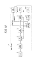
以下、本発明を適用した実施形態について、図面を参照して説明する。図1は、本発明の一実施形態に係るカラーフィルタアレイを有する撮像素子が設けられたデジタルカメラの概略構成を示すブロック図である。 Embodiments to which the present invention is applied will be described below with reference to the drawings. FIG. 1 is a block diagram showing a schematic configuration of a digital camera provided with an image sensor having a color filter array according to an embodiment of the present invention.
デジタルカメラ10は、撮影光学系11、撮像素子20、センサ駆動部12、システムバス13、画像信号処理部30、バッファメモリ14、システムコントローラ15、画像表示部16、画像記録部17、及び操作部18などによって構成される。
The
撮影光学系11は、光軸が撮像素子20の受光部21の中心を通るように垂直に配置され、撮像素子20に結合される。撮影光学系11は複数のレンズ(図示せず)によって構成され、被写体の光学像を受光部21に結像させる。なお、撮影光学系11は、デジタルカメラ10に固定されていてもよいし、着脱可能な交換式であってもよい。
The photographing optical system 11 is vertically arranged so that the optical axis passes through the center of the
撮像素子20は、例えばCMOSエリアセンサであり、受光部21、垂直走査回路22、水平読出回路23、及びA/Dコンバータ24によって構成される。前述のように、撮影光学系11により被写体の光学像が受光部21に形成される。
The
受光部21には、マトリックス状に複数の画素(図示せず)が配置される。また、受光部21上において、OB(オプティカルブラック)領域21bと有効撮影領域21eとが定められる。OB領域21bに配置されるOB画素は受光面が遮光されており、黒色の基準となる暗電流をOB画素信号として出力する。また、有効撮影領域21eはCFA(図1において図示せず)によって覆われており、各画素は5バンドのカラーフィルタのいずれかによって覆われる。
In the
図2に示すように、CFA21aにはG(グリーン)カラーフィルタ、Cy(シアン)カラーフィルタ、Or(オレンジ)カラーフィルタ、B(ブルー)カラーフィルタ、及びR(レッド)カラーフィルタの5バンドのカラーフィルタが設けられる。したがって、各画素では、対応するカラーフィルタの透過バンドの光の受光量に応じた画素信号が生成される。なお、図3に示すように、G、Cy、Or、B、Rカラーフィルタは、異なる分光感度特性を有する。なお、本実施形態において分光感度特性が異なるとは、ピーク波長の値、または半値幅の中心値が異なることを意味する。
As shown in FIG. 2, the
CFA21aでは、4行4列のカラーフィルタ繰返し単位21uが行方向及び列方向に繰返し配置される。図2に示すように、カラーフィルタ繰返し単位21u内には、8個のGカラーフィルタ、2個のCyカラーフィルタ、2個のOrカラーフィルタ、2個のBカラーフィルタ、及び2個のRカラーフィルタが配置される。
In the
CFA21aでは、Cyカラーフィルタ、Orカラーフィルタ、Bカラーフィルタ、及びRカラーフィルタのいずれかと、Gカラーフィルタとが市松模様状に配置される。すなわち、Gカラーフィルタは全行全列において、1画素おきに繰返し配置される。例えば、図2における左上を基準として、1、3行目には2、4列目にGカラーフィルタが配置される。また、2、4行目には、1、3列目にGカラーフィルタが配置される。
In the
また、Gカラーフィルタ、Bカラーフィルタ、及びCyカラーフィルタが並ぶ行及び列が、列方向及び行方向に1画素おきに繰返し配置される。例えば、図2において、1行1列目及び3行3列目にBカラーフィルタが配置され、1行3列目及び3行1列目にCyカラーフィルタが配置される。 A row and a column in which the G color filter, the B color filter, and the Cy color filter are arranged are repeatedly arranged every other pixel in the column direction and the row direction. For example, in FIG. 2, a B color filter is arranged in the first row, first column and the third row, third column, and a Cy color filter is arranged in the first row, third column, and the third row, first column.
また、Gカラーフィルタ、Rカラーフィルタ、及びOrカラーフィルタが並ぶ行及び列が、行方向及び列方向に1画素おきに繰返し配置される。例えば、図2において、2行4列目及び4行2列目にRカラーフィルタが配置され、2行2列目及び3行3列目にOrカラーフィルタが配置される。 A row and a column in which the G color filter, the R color filter, and the Or color filter are arranged are repeatedly arranged every other pixel in the row direction and the column direction. For example, in FIG. 2, the R color filter is arranged at the second row, the fourth column, and the fourth row, the second column, and the Or color filter is arranged at the second row, the second column, and the third row, the third column.
上述のようなカラーフィルタ繰返し単位では、Gカラーフィルタの割合が最大であり全体の50%を占めている。また、任意の位置の画素において、斜め方向に隣接する画素に対応するカラーフィルタのバンドは等しい。 In the color filter repeating unit as described above, the ratio of the G color filter is the largest, accounting for 50% of the whole. In addition, in the pixel at an arbitrary position, the bands of the color filters corresponding to the pixels adjacent in the oblique direction are equal.
例えば、図2に示すように、いずれのGカラーフィルタにおいても、斜方に隣接するカラーフィルタはすべてGカラーフィルタである。したがって、任意のGカラーフィルタの右斜め上及び左斜め下にはGカラーフィルタが配置され、互いに同じバンドのカラーフィルタである。また、右斜め下及び左斜め上にはGカラーフィタが配置され、互いに同じバンドのカラーフィルタである。 For example, as shown in FIG. 2, in any G color filter, all the color filters adjacent in the oblique direction are G color filters. Accordingly, the G color filters are arranged on the upper right and lower left sides of any G color filter, and are color filters of the same band. Further, G color filters are arranged on the lower right and upper left sides, which are color filters of the same band.
また、いずれのCyカラーフィルタにおいても、斜方に沿ってRカラーフィルタまたはOrカラーフィルタによって挟まれる。詳細に説明すると、任意のCyカラーフィルタの右斜め上及び左斜め下にはOrカラーフィルタが配置され、互いに同じバンドのカラーフィルタである。また、右斜め下及び左斜め上にはRカラーフィルタが配置され、互いに同じバンドのカラーフィルタである。 Also, any Cy color filter is sandwiched between the R color filter and the Or color filter along the oblique direction. More specifically, an Or color filter is disposed on the upper right and lower left sides of an arbitrary Cy color filter, and the color filters have the same band. Further, R color filters are arranged on the lower right and upper left sides, and are color filters of the same band.
Orカラーフィルタ、Bカラーフィルタ、及びRカラーフィルタにおいても、同様であって、斜め方向に隣接するカラーフィルタ同士は同じバンドのカラーフィルタとなる。 The same applies to the Or color filter, the B color filter, and the R color filter, and the color filters adjacent in the oblique direction are the color filters of the same band.
上述のようなCFA21aが設けられた画素において、透過したバンドの光の受光量に応じた画素信号が生成される。垂直走査回路22により画素信号を出力させる画素の行が選択され、水平読出回路23により画素信号を出力させる画素の列が選択される(図1参照)。
In the pixel provided with the
垂直走査回路22及び水平読出回路23はセンサ駆動部12に駆動される。デジタルカメラ10には、通常読出しモードと、第1〜第3の間引き読出しモードが設けられる。それぞれのモードにおいて、読出す全画素から1画素ずつ画素信号が出力されるように、垂直走査回路22及び水平読出回路23は制御される。出力された画素信号はA/Dコンバータ24によりデジタル信号に変換される。受光部21に配置されるすべての画素の画素信号が1フレームのRAWデータが原画像信号に定められる。
The vertical scanning circuit 22 and the
なお、静止画を撮影するとき等のように高い解像度が求められる場合に、通常読出しモードで撮像素子20は駆動され、全画素から画素信号が生成される。また、撮影待機中における調光及び合焦動作のための情報の検出時や、動画像の撮影時等のように高い動解像度が求められる場合に第1〜第3の間引き読出しモードで撮像素子20は駆動される。
When a high resolution is required, such as when shooting a still image, the
第1の間引き読出しモードでは、図4に示すように、3行3列に並ぶ画素pxによって構成される第1の画素ブロックpb1毎に、第1の画素ブロックpb1の中心の画素pxのみから画素信号が出力される。 In the first thinning-out readout mode, as shown in FIG. 4, for each first pixel block pb1 configured by pixels px arranged in 3 rows and 3 columns, only pixels from the center pixel px of the first pixel block pb1 are used. A signal is output.
なお、第1の画素ブロックpb1が出力する画素信号の色信号成分を第1の画素ブロックpb1のカラーフィルタの種類とみなすと、図5に示すように、第1の画素ブロックpb1のカラーフィルタの配列は、CFA21aにおけるカラーフィルタの配列と同じである。したがって、第1の間引き読出しモードで出力させた原画像信号は、画像信号処理部30において通常読出しモードで出力させた原画像信号と同じ画像処理を施すことが可能である。
If the color signal component of the pixel signal output from the first pixel block pb1 is regarded as the type of the color filter of the first pixel block pb1, the color filter component of the first pixel block pb1 as shown in FIG. The arrangement is the same as the arrangement of color filters in the
第2の間引き読出しモードでは、図6に示すように、5行5列に並ぶ画素pxによって構成される第2の画素ブロックpb2毎に、第2の画素ブロックpb2の中心の画素pxのみから画素信号が出力される。 In the second thinning-out readout mode, as shown in FIG. 6, for each second pixel block pb2 constituted by pixels px arranged in 5 rows and 5 columns, only pixels px from the center pixel px of the second pixel block pb2 are used. A signal is output.
なお、第2の画素ブロックpb2が出力する画素信号の色信号成分を第2の画素ブロックpb2のカラーフィルタの種類とみなすと、図7に示すように、第2の画素ブロックpb2のカラーフィルタの配列は、CFA21aにおけるカラーフィルタの配列と同じである。したがって、第2の間引き読出しモードで出力させた原画像信号は、画像信号処理部30において通常読出しモードで出力させた原画像信号と同じ画像処理を施すことが可能である。
If the color signal component of the pixel signal output from the second pixel block pb2 is regarded as the type of the color filter of the second pixel block pb2, as shown in FIG. 7, the color filter component of the second pixel block pb2 The arrangement is the same as the arrangement of color filters in the
第3の間引き読出しモードでは、図8に示すように、7行7列に並ぶ画素pxによって構成される第3の画素ブロックpb3毎に、第3の画素ブロックpb3の中心の画素pxのみから画素信号が出力される。 In the third thinning-out reading mode, as shown in FIG. 8, for each third pixel block pb3 configured by pixels px arranged in 7 rows and 7 columns, pixels from only the pixel px at the center of the third pixel block pb3 are used. A signal is output.
なお、第3の画素ブロックpb3が出力する画素信号の色信号成分を第3の画素ブロックpb3のカラーフィルタの種類とみなすと、図9に示すように、第3の画素ブロックpb3のカラーフィルタの配列は、CFA21aにおけるカラーフィルタの配列と同じである。したがって、第3の間引き読出しモードで出力させた原画像信号は、画像信号処理部30において通常読出しモードで出力させた原画像信号と同じ画像処理を施すことが可能である。
If the color signal component of the pixel signal output from the third pixel block pb3 is regarded as the type of the color filter of the third pixel block pb3, the color filter component of the third pixel block pb3 is shown in FIG. The arrangement is the same as the arrangement of color filters in the
なお、画素ブロックが大きくなるほど、すなわち画素ブロックに含まれる画素の数が多くなると、読出し速度は速くなる一方で解像度は低下する。それゆえ、要求される読出し速度または解像度に応じて第1〜第3の間引き読出しモードは選択される。 Note that as the pixel block becomes larger, that is, as the number of pixels included in the pixel block increases, the reading speed increases and the resolution decreases. Therefore, the first to third decimation readout modes are selected according to the required readout speed or resolution.
撮像素子20、バッファメモリ14、画像信号処理部30、システムコントローラ15、画像表示部16、画像記録部17、操作部18、及びセンサ駆動部12は、システムバス13を介して電気的に接続される(図1参照)。システムバス13に接続されるこれらの部位は、システムバス13を介して互いに様々な信号やデータを送受信することが可能である。
The
撮像素子20から出力される原画像信号はバッファメモリ14に送信され、格納される。バッファメモリ14はSDRAM等であって、比較的高速なアクセス速度を有し、画像信号処理部30のワークエリアとして用いられる。また、バッファメモリ14は、システムコントローラ15がデジタルカメラ10の各部位を制御するためのプログラムを実行する際のワークエリアとしても用いられる。
The original image signal output from the
画像信号処理部30は、後に詳細に説明するデモザイキング処理を原画像信号に施し、補間画像信号を生成する。さらに、画像信号処理部30は、補間画像信号に対して所定の画像処理を施す。なお、補間画像信号は必要に応じて、RGB画像信号に変換される。
The image
所定の画像処理の施された補間画像信号およびRGB画像信号は、画像表示部16に送信される。画像表示部16は多原色モニタ(図1において図示せず)及びRGBモニタ(図1において図示せず)を有している。多原色モニタ及びRGBモニタはカラー液晶表示素子(図示せず)やバックライト装置(図示せず)を備え、補間画像信号及びRGB画像信号に相当する画像が表示される。
The interpolated image signal and the RGB image signal subjected to the predetermined image processing are transmitted to the
なお、画像表示部16は、デジタルカメラ10の背面や側面に設けられる。また、画像表示部16は、比較的小型の表示素子(図示せず)と拡大光学系(図示せず)とで構成されるEVF(電子ビューファインダ)であってもよい。さらには両方の形態を有し、使用状況に応じて切替え可能に構成されてもよい。また、画像表示部16は、有機EL表示素子等であってもよい。
The
画像信号処理部30から出力される補間画像信号及びRGB画像信号は、画像記録部17にも送信され、格納される。なお、画像記録部17は、内蔵式或いはコネクタ(図示せず)を介して接続可能なフラッシュメモリである。
The interpolated image signal and the RGB image signal output from the image
デジタルカメラ10の各部位は、システムコントローラ15によって制御される。各部位を制御するための制御信号がシステムコントローラ15からシステムバス13を介して各部位に入力される。
Each part of the
なお、画像信号処理部30及びシステムコントローラ15は、CPU(中央処理装置)等の任意の好適なプロセッサ上で実行されるソフトウェアとして構成したり、処理ごとに特化した専用のプロセッサによって構成したりすることもできる。
The image
システムコントローラ15は、パワーボタン(図示せず)、レリーズボタン(図示せず)、及びダイヤル(図示せず)などの入力機構を有する入力部18に接続される。使用者によるデジタルカメラ10の様々な操作入力が入力部18に検知される。入力部18に検知される操作入力に応じて、システムコントローラ15はデジタルカメラ10の各部位を制御する。
The system controller 15 is connected to an
次に、画像信号処理部30の構成について図10を用いて説明する。画像信号処理部30は、OB減算処理部31、マルチバンド(MB)デモザイク処理部40(画像処理システム)、NR処理部32、MB−RGB変換部33、色変換処理部34、及び色ガンマ補正処理部35によって構成される。
Next, the configuration of the image
バッファメモリ14から出力される原画像信号は、OB減算処理部31に送信される。OB減算処理部31では、OB画素に生成されたOB画素信号によって各画素信号を減じることによって各画素信号の黒レベルの調整を行う。
The original image signal output from the
OB減算処理部31から出力される画素信号はMBデモザイク処理部40に送信される。前述のように、原画像信号を構成する画素信号は5バンドの中のいずれか一つの色信号成分のみを有する。すなわち、原画像信号は、図11に示すように、G原画像信号成分((a)参照)、Cy原画像信号成分((b)参照)、Or原画像信号成分((c)参照)、B原画像信号成分((d)参照)、R原画像信号成分((e)参照)によって構成される。後述するようにMBデモザイク処理部40におけるデモザイク処理により、全色信号成分が補間される。すなわち、全画素信号は5つの色信号成分を有するように、補間される。
The pixel signal output from the OB
デモザイク処理の施された原画像信号は、補間画像信号としてNR処理部32に送信される(図10参照)。NR処理部32においてコアリング処理やメディアンフィルタ処理等のノイズ低減化処理が実行され、補間画像信号からノイズが除去される。ノイズの除去された補間画像信号は、一時的にバッファメモリ14に格納される。
The original image signal subjected to the demosaic process is transmitted to the
デジタルカメラ10が補間画像信号を記録する記録モードに設定されている場合には、バッファメモリ14に格納された補間画像信号に、必要に応じて圧縮処理が施され、所定のフォーマットに応じて生成された補間画像ファイルとして画像記録部17に格納される。
When the
なお、補間画像ファイル中には、後に画像を再生するときに参照される色再現情報がタグ情報として付加される。なお、色再現情報としては、撮影光学系11の分光透過率、撮像素子20の分光感度、撮影時に被写体に照射した光の分光放射輝度、被写体の分光反射率を推定する処理のために参照される被写体固有の統計情報などが含まれる。
In the interpolated image file, color reproduction information that is referred to later when an image is reproduced is added as tag information. The color reproduction information is referred to for processing for estimating the spectral transmittance of the photographing optical system 11, the spectral sensitivity of the
デジタルカメラ10の動作モードがマルチバンドの画像を再生する画像再生モードに設定されている場合、NR処理部32によりノイズの除去された補間画像信号は色変換処理部34に送信される。
When the operation mode of the
色変換処理部34は、多原色モニタ16mbのモニタプロファイル等に関する情報(モニタプロファイル情報)を予め取得する。また、色変換処理部34は、デジタルカメラ10の周囲の照明光の分光放射輝度に関する情報(観察照明分光分布情報)を多原色モニタ16mbの近傍に設けられた光センサ(図示せず)から取得する。色変換処理部34は、モニタプロファイル情報及び観察照明分光分布情報を用いて補間画像信号に色変換処理を施す。色変換処理の施された補間画像信号は、多原色モニタ16mbに送信される。
The color
上述の色変換処理により、被写体がデジタルカメラ10の周囲の照明光で照射されているような色合いで、多原色モニタ16mbに表示される。それゆえ、使用者は再現性を向上させた画像を観察可能である。
By the above-described color conversion processing, the subject is displayed on the multi-primary color monitor 16mb in a hue such that the subject is illuminated with illumination light around the
デジタルカメラ10では、従来のRGBのみを色信号成分として有するRGB画像信号を格納及び表示可能である。デジタルカメラ10がRGB画像信号を記録する記録モードに設定されている場合には、ノイズの除去された補間画像信号がMB−RGB変換処理部33に送信される。
The
MB−RGB変換処理部33では、補間画像信号に対してRGB変換処理が施される。5バンドの色信号成分によって構成される補間画像信号が、RGBの3バンドの色信号成分によって構成されるRGB画像信号に変換される。RGB画像信号は、一時的にバッファメモリ14に格納され、必要に応じて圧縮処理が施され、所定のフォーマットに応じて生成されたRGB画像ファイルとして画像記録部17に格納される。
The MB-RGB
デジタルカメラ10がRGBの3バンドの画像を再生する画像再生モードに設定されている場合には、RGB画像信号は色・ガンマ補正処理部35に送信される。色・ガンマ補正処理部35は、RGBモニタ16rgbのモニタプロファイルを予め取得する。色・ガンマ補正処理部35では、取得したモニタプロファイルを用いてRGB画像信号に対して色補正処理及びガンマ補正処理を施す。これらの補正処理が施されたRGB画像信号はRGBモニタ16rgbに送信され、RGB画像信号に相当する画像が表示される。
When the
次に、デモザイク処理について図12を用いて説明する。図12は、MBデモザイク処理部40によって実行されるデモザイク処理を説明するための概念図である。
Next, demosaic processing will be described with reference to FIG. FIG. 12 is a conceptual diagram for explaining the demosaic process executed by the
前述のように、原画像信号OISは各画素信号が5バンドのいずれかの色信号成分のみを有している。原画像信号OISは、G原画像信号成分gOIS、Cy原画像信号成分cyOIS、Or原画像信号成分orOIS、B原画像信号成分bOIS、及びR原画像信号成分rOISに分割される。 As described above, in the original image signal OIS, each pixel signal has only one of the color signal components of 5 bands. The original image signal OIS is divided into a G original image signal component gOIS, a Cy original image signal component cyOIS, an Or original image signal component orOIS, a B original image signal component bOIS, and an R original image signal component rOIS.
また、原画像信号OISの全画素信号を用いて全画素に対して適応的カーネル関数が算出される(図12における“aK”参照)。適応的カーネル関数と、G原画像信号成分gOISとを用いて適応的ガウシアン補間法によりG原画像信号成分gOISにおける欠落した画素信号が補間され、参照画像信号RIS(一次参照画像)が生成される(図12における“aGU”参照)。 Also, an adaptive kernel function is calculated for all pixels using all pixel signals of the original image signal OIS (see “aK” in FIG. 12). A missing pixel signal in the G original image signal component gOIS is interpolated by an adaptive Gaussian interpolation method using the adaptive kernel function and the G original image signal component gOIS, and a reference image signal RIS (primary reference image) is generated. (See “aGU” in FIG. 12).
適応的カーネル関数、参照画像信号RIS、及びG原画像信号成分gOISを用いて適応的ジョイントバイラテラル補間法(図12における“aJBU”参照)によりG原画像信号成分gOISにおける欠落した画素信号が補間され、G補間画像信号成分gIISが生成される。 Using the adaptive kernel function, the reference image signal RIS, and the G original image signal component gOIS, the missing pixel signal in the G original image signal component gOIS is interpolated by an adaptive joint bilateral interpolation method (see “aJBU” in FIG. 12). Then, the G interpolation image signal component gIIS is generated.
G原画像信号成分gOISの代わりに、Cy原画像信号成分cyOISを用いて同様の処理を施すことによりCy補間画像信号成分cyIISが生成される。同様にして、Or補間画像信号成分orIIS、B補間画像信号成分bIIS、及びR補間画像信号成分rIISが生成される。全色信号成分を有する画素信号を全画素に対して生成することにより補間画像信号IISが生成される。 A Cy-interpolated image signal component cyIIS is generated by performing similar processing using the Cy original image signal component cyOIS instead of the G original image signal component gOIS. Similarly, an Or interpolation image signal component orIIS, a B interpolation image signal component bIIS, and an R interpolation image signal component rIIS are generated. An interpolated image signal IIS is generated by generating pixel signals having all color signal components for all pixels.
次に、このようなデモザイク処理を実行するMBデモザイク処理部40の構成及び機能を、図13を用いて説明する。MBデモザイク処理部40は、分配部41、微分値算出部42、適応的カーネル算出部43、参照画像作成部44、及び補間画像作成部45によって構成される。
Next, the configuration and function of the MB
MBデモザイク処理部40に受信される原画像信号は、分配部41に入力される。分配部41では、微分値算出部42、参照画像作成部44、及び補間画像作成部45に、必要に応じた色信号成分が分配される。
The original image signal received by the MB
微分値算出部42には、原画像信号を構成する全画素信号が送信される。微分値算出部42では、画素毎に2方向の微分値(微分情報)が算出される。微分値の算出のために、全画素が順番に注目画素に指定される。指定された注目画素の右斜め上及び左斜め下に隣接する画素の画素信号の差と、右斜め下及び左斜め上に隣接する画素の画素信号の差とが微分値として算出される。 All the pixel signals constituting the original image signal are transmitted to the differential value calculation unit 42. The differential value calculation unit 42 calculates a differential value (differential information) in two directions for each pixel. In order to calculate the differential value, all the pixels are sequentially designated as the target pixel. A difference between pixel signals of pixels adjacent to the upper right and lower left of the designated target pixel and a difference between pixel signals of pixels adjacent to the lower right and upper left are calculated as differential values.
なお、前述のように、いずれの画素を注目画素とする場合でも、右斜め上及び左斜め下の画素では同じ色信号成分の画素信号が生成され、右斜め下及び左斜め上の画素では同じ色信号成分の画素信号が生成される。それゆえ、上述の微分値は、注目画素を中心とする局所的な画像における両斜め方向の勾配を示している。全画素に対して算出された微分値は、適応的カーネル算出部43に送信される。
As described above, regardless of which pixel is the target pixel, pixel signals having the same color signal component are generated in the upper right and lower left pixels, and the same in the lower right and upper left pixels. A color signal component pixel signal is generated. Therefore, the above-described differential value indicates a gradient in both oblique directions in a local image centered on the target pixel. The differential values calculated for all the pixels are transmitted to the adaptive
なお、全画素に対して算出された微分値は、適応的カーネル算出部43だけでなく、NR処理部32、MB−RGB変換処理部33、色変換処理部34、及び色・ガンマ補正処理部35にも送信される。微分値は、それぞれの部位における処理に用いられる。
The differential values calculated for all the pixels are not only the adaptive
適応的カーネル算出部43では、微分値に基づいて、画素毎に適応的カーネル関数が算出される。適応的カーネル関数の算出のために、すべての画素が順番に注目画素に指定される。また、注目画素を中心とする注目画素の周囲の7行7列に配置される画素が周囲画素に指定される。注目画素及び周囲画素の指定を終えると、注目画素に対する共分散行列Cxの逆行列が算出される。
The adaptive
逆行列は、(1)式に注目画素及び周囲画素の微分値を代入することにより算出される。 The inverse matrix is calculated by substituting the differential values of the pixel of interest and the surrounding pixels into equation (1).

なお、(1)式において、Nxは周囲画素の画素位置集合であり、|Nx|は画素位置集合の画素数である。また、Zu(xj)は、周囲画素xjのu方向の微分値であり、Zv(xj)は周囲画素xjのv方向の微分値である。なお、図2に示すように、u方向とは右斜め下から左斜め上に向かう方向であり、v方向とは左斜め下から右斜め上に向かう方向である。In Equation (1), N x is a pixel position set of surrounding pixels, and | N x | is the number of pixels in the pixel position set. Z u (x j ) is a differential value of the surrounding pixel x j in the u direction, and Z v (x j ) is a differential value of the surrounding pixel x j in the v direction. As shown in FIG. 2, the u direction is a direction from the lower right to the upper left, and the v direction is a direction from the lower left to the upper right.
注目画素の共分散行列が算出されると、次に注目画素に対するカーネル関数の大きさを表すパラメータμxが算出される。パラメータμxの算出のために、共分散行列Cxの固有値λ1、λ2が算出される。固有値の積λ1×λ2が閾値Sと比較される。固有値の積λ1×λ2が閾値S以上である場合には、パラメータμxは1と計算される。一方、固有値の積λ1×λ2が閾値Sより小さい場合には、(S/(λ1×λ2))の四乗根がパラメータμxとして計算される。When the covariance matrix of the target pixel is calculated, a parameter μ x representing the magnitude of the kernel function for the target pixel is calculated next. In order to calculate the parameter μ x , eigenvalues λ 1 and λ 2 of the covariance matrix C x are calculated. The product of eigenvalues λ 1 × λ 2 is compared with the threshold value S. If the eigenvalue product λ 1 × λ 2 is greater than or equal to the threshold S, the parameter μ x is calculated as 1. On the other hand, when the product of the eigenvalues λ 1 × λ 2 is smaller than the threshold value S, the fourth root of (S / (λ 1 × λ 2 )) is calculated as the parameter μ x .
パラメータμxの算出後、注目画素に対する適当的カーネル関数が算出される。適応的カーネル関数kx(xj−x)は(2)式により算出される。After calculating the parameter μ x , an appropriate kernel function for the target pixel is calculated. The adaptive kernel function k x (x j −x) is calculated by the equation (2).
(2)式において、xjは周囲画素の座標であり、xは注目画素の座標であり、Rは45°の回転行列であり、hは所定の設計パラメータであり、例えば1に定められる。In equation (2), x j is the coordinates of the surrounding pixels, x is the coordinates of the pixel of interest, R is a 45 ° rotation matrix, h is a predetermined design parameter, and is set to 1, for example.
全画素に対して算出された適応的カーネル関数kx(xj−x)は、参照画像作成部44及び補間画像作成部45に送信される。参照画像作成部44では、原画像信号中に最も要素数の多いG色信号成分(第1の色信号成分)が分配部41から送信される。参照画像作成部44では、適応的ガウシアン補間法により全体の1/2の画素に対してのみ存在するG色信号成分の補間が行われ、参照画像信号が生成される。The adaptive kernel function k x (x j −x) calculated for all pixels is transmitted to the reference
適応的ガウシアン補間法を用いたG原画像信号成分における欠落した画素信号の補間について説明する。G原画像信号成分において補間される画素、すなわち原画像信号においてG色信号成分を有さない画素が順番に注目画素に指定される。注目画素を中心とする注目画素の周囲の7行7列の画素が周囲画素に指定される。 Interpolation of the missing pixel signal in the G original image signal component using the adaptive Gaussian interpolation method will be described. A pixel to be interpolated in the G original image signal component, that is, a pixel having no G color signal component in the original image signal is sequentially designated as the target pixel. A pixel in 7 rows and 7 columns around the pixel of interest centered on the pixel of interest is designated as the surrounding pixel.
注目画素の画素信号は、周囲画素のG色信号成分及び適応的カーネル関数に基づいて(3)式により算出される。 The pixel signal of the pixel of interest is calculated by equation (3) based on the G color signal component of the surrounding pixels and the adaptive kernel function.
なお、ωxは(4)式により算出される。Mxiはバイナリマスクであり、周囲画素がG色信号成分を有するときに1であり、周囲画素がG色信号成分を有さないときには0である。Sxiは周囲画素のG色信号成分である。Note that ω x is calculated by equation (4). M xi is a binary mask, which is 1 when surrounding pixels have a G color signal component, and 0 when surrounding pixels do not have a G color signal component. S xi is a G color signal component of surrounding pixels.
注目画素に指定された全画素に対して補間されたG色信号成分と、G原画像信号成分とにより構成される参照画像信号は、補間画像作成部45に送信される。補間画像作成部45には、前述のように適応的カーネル関数kx(xi−x)、及び参照画像信号が適応的カーネル算出部43及び参照画像作成部44から送信される。また、前述のように、補間画像作成部45には、分配部41からG原画像信号成分、Cy原画像信号成分、Or原画像信号成分、B原画像信号成分、及びR原画像信号成分が順番に送信される。The reference image signal composed of the G color signal component interpolated for all the pixels designated as the target pixel and the G original image signal component is transmitted to the interpolated
補間画像作成部45では、適応的ジョイントバイラテラレル補間法により、生成されていない色信号成分が全画素に対して補間される。例えば、全体の1/2の画素に対してのみ存在するG色信号成分を用いて、他の画素のG色信号成分が補間される。
In the interpolated
同様に、それぞれ1/8の画素に対してのみ存在するCy色信号成分、Or色信号成分、B色信号成分、及びR色信号成分を用いて、他の画素のCy色信号成分、Or色信号成分、B色信号成分、及びR色信号成分が補間される。全色信号成分の補間により、全色信号成分を有する全画素信号によって構成される補間画像信号が生成される。なお、G色信号成分に関しては参照画像の作成において補間されているが、参照画像を用いた補間が別に行われる。 Similarly, using the Cy color signal component, the Or color signal component, the B color signal component, and the R color signal component that exist only for each 1/8 pixel, the Cy color signal component and Or color of other pixels are used. The signal component, the B color signal component, and the R color signal component are interpolated. By interpolation of all color signal components, an interpolated image signal composed of all pixel signals having all color signal components is generated. Note that although the G color signal component is interpolated in the creation of the reference image, interpolation using the reference image is performed separately.
適応的ジョイントバイラテラル補間法を用いた各色信号成分の補間について、G色信号成分を例にして説明する。G色信号成分の補間が行われるべき画素、すなわち原画像信号においてG色信号成分を有さない画素が順番に注目画素に指定される。注目画素を中心とする注目画素の周囲の7行7列の画素が周囲画素に指定される。 Interpolation of each color signal component using the adaptive joint bilateral interpolation method will be described using the G color signal component as an example. A pixel to be interpolated with the G color signal component, that is, a pixel having no G color signal component in the original image signal is sequentially designated as the target pixel. A pixel in 7 rows and 7 columns around the pixel of interest centered on the pixel of interest is designated as the surrounding pixel.
注目画素の色信号成分は、周囲画素のG色信号成分、適応的カーネル関数、及び参照画像信号に基づいて(5)式により算出される。 The color signal component of the target pixel is calculated by the equation (5) based on the G color signal component of the surrounding pixels, the adaptive kernel function, and the reference image signal.
なお、(5)式において、Ixiは参照画像における周囲画素の画素値、Ixは参照画像における注目画素の画素値である。r(Ixi−Ix)は、注目画素と周囲画素との画素値の差分に応じた重み付けである。In equation (5), I xi is the pixel value of surrounding pixels in the reference image, and I x is the pixel value of the pixel of interest in the reference image. r (I xi −I x ) is a weight according to the difference in pixel value between the target pixel and the surrounding pixels.
注目画素に対するG色信号成分の補間により、G補間画像信号成分が生成される。以後、同様にCy色信号成分、Or色信号成分、B色信号成分、及びR色信号成分もG色信号成分と同様に補間が行われ、Cy補間画像信号成分、Or補間画像信号成分、B補間画像信号成分、及びR補間画像信号成分が生成される。このように全色信号成分の補間により補間画像信号が生成される。 A G-interpolated image signal component is generated by interpolation of the G color signal component with respect to the pixel of interest. Thereafter, similarly, the Cy color signal component, the Or color signal component, the B color signal component, and the R color signal component are also interpolated in the same manner as the G color signal component, and the Cy interpolation image signal component, the Or interpolation image signal component, B An interpolated image signal component and an R interpolated image signal component are generated. In this way, an interpolated image signal is generated by interpolation of all color signal components.
以上のような構成の第1の実施形態のCFAによれば、5バンド以上のカラーフィルタを有しながら、色補間を行う前に全画素に対する共通の2方向の微分値、即ち勾配情報を取得することが可能である。 According to the CFA of the first embodiment configured as described above, a common two-direction differential value for all pixels, that is, gradient information, is acquired before performing color interpolation while having a color filter of 5 bands or more. Is possible.
一般的に自然画像では、高周波成分においてバンド間の相関が強いことが知られている。したがって、各バンドの画像は同じエッジ構造を有する。そこで、すべてのバンドの勾配情報は等しいと仮定される。それゆえ、何れの色信号成分の微分値であっても、後の画像処理などに用いるのに十分な精度が得られる。本実施形態のように微分値を取得する2色同士の相関が高い場合には、より高精度な情報を取得可能である。 In general, it is known that a natural image has a strong correlation between bands in a high frequency component. Therefore, each band image has the same edge structure. Therefore, it is assumed that the gradient information of all bands is equal. Therefore, any differential value of any color signal component can be obtained with sufficient accuracy to be used for subsequent image processing. When the correlation between the two colors from which the differential value is acquired is high as in the present embodiment, more accurate information can be acquired.
さらに、全画素で共通の方向の微分値を取得することにより、画素毎に異なる方向の微分値を取得する場合に比べて、処理の簡素化が可能である。また、勾配情報の方向を合わせるための変換による高周波成分の情報欠落を低減化した高精度の勾配情報を取得可能である。 Furthermore, by obtaining a differential value in a common direction for all the pixels, it is possible to simplify the processing compared to obtaining a differential value in a different direction for each pixel. In addition, it is possible to acquire high-precision gradient information in which missing information of high-frequency components due to conversion for adjusting the direction of gradient information is reduced.
精度の高い勾配情報を用いれば、上述のように欠落する色信号成分の補間に用いることによって偽色の発生を低減化する補間が可能である。さらに、精度の高い勾配情報を用いることにより、精度の高いノイズ除去処理、マルチバンドからRGBへの変換処理、色変換処理、及び色・ガンマ補正処理を実行することが可能である。 If highly accurate gradient information is used, it is possible to perform interpolation that reduces the occurrence of false colors by using it for interpolation of missing color signal components as described above. Further, by using highly accurate gradient information, it is possible to execute highly accurate noise removal processing, multiband to RGB conversion processing, color conversion processing, and color / gamma correction processing.
本発明を諸図面や実施例に基づき説明してきたが、当業者であれば本開示に基づき種々の変形や修正を行うことが容易であることに注意されたい。したがって、これらの変形や修正は本発明の範囲に含まれることに留意されたい。 Although the present invention has been described based on the drawings and examples, it should be noted that those skilled in the art can easily make various modifications and corrections based on the present disclosure. Therefore, it should be noted that these variations and modifications are included in the scope of the present invention.
例えば、上記の実施形態において、5バンドのカラーフィルタ配置が定められているが、任意の画素を挟む2画素のカラーフィルタが同じとなるようなカラーフィルタの配置であれば、本実施形態と同様の効果が得られる。 For example, in the above embodiment, a 5-band color filter arrangement is defined. However, if the color filter arrangement is such that the color filters of 2 pixels sandwiching an arbitrary pixel are the same, the same as in this embodiment. The effect is obtained.
例えば、図14に示すようにG、Cy、Or、B、Rカラーフィルタを配置したCFA2100aであっても、本実施形態と同様の効果が得られる。CFA2100aでは、何れの画素を注目画素としても微分値の算出に用いる画素に必ず相関の高い色が含まれる。すなわち、Orカラーフィルタの斜方には必ずRカラーフィルタが配置されている。微分値を算出する際に相関の高い色が必ず含まれることにより、高精度の微分値を算出可能である。
For example, even if the
また、図15に示すように、G、Cy、Or、B、Rカラーフィルタを配置したCFA2101aであっても、すべての画素において右斜め上と左斜め下の画素のカラーフィルタのバンドは同じであり、左斜め上と右斜め下の画素pxのカラーフィルタのバンドも同じである。したがって、本実施形態のように、原画像信号から直接微分値を算出することが可能である。
Further, as shown in FIG. 15, even in the
また、CFA2101aにおいても、本実施形態のように間引き読出しも可能である。例えば、図16に示すように、3行3列に並ぶ画素pxによって構成される第1の画素ブロックpb1毎に画素信号を読出すことも可能である。本実施形態と同様に、第1の画素ブロックpb1の中心の画素pxのカラーフィルタの種類を第1の画素ブロックpb1のカラーフィルタの種類とみなして、第1の画素ブロックpb1のカラーフィルタの配列は、CFA21aの配列と同じとなる。
The
さらには、例えば、図17に示すように、5行5列に並ぶ画素pxによって構成される第2の画素ブロックpb2毎に画素信号を読出すことも可能である。本実施形態と同様に、第2の画素ブロックpb2の中心の画素pxのカラーフィルタの種類を第2の画素ブロックpb2のカラーフィルタの種類とみなして、第2の画素ブロックpb2のカラーフィルタの配列は、CFA21aの配列と同じである。 Furthermore, for example, as shown in FIG. 17, it is also possible to read out pixel signals for each second pixel block pb2 constituted by pixels px arranged in 5 rows and 5 columns. Similar to the present embodiment, the color filter type of the pixel px at the center of the second pixel block pb2 is regarded as the type of color filter of the second pixel block pb2, and the arrangement of the color filters of the second pixel block pb2 Is the same as the sequence of CFA21a.
また、本実施形態においては、注目画素の微分値の算出に用いる2画素は注目画素に隣接する構成であるが、注目画素から等間隔であれば隣接しなくてもよい。例えば、注目画素から2画素分右で2画素分上の画素と、2画素分左で2画素分下の画素との差分を算出することにより微分値を算出してもよい。 In the present embodiment, the two pixels used for calculating the differential value of the target pixel are adjacent to the target pixel, but may not be adjacent if they are equidistant from the target pixel. For example, the differential value may be calculated by calculating a difference between a pixel two pixels on the right and two pixels above the target pixel and a pixel two pixels on the left and two pixels below.
注目画素に隣接する画素から、全画素に対して共通の方向の微分値を取得可能なカラーフィルタの種類は5〜8種類に限定される。一方で、注目画素から等間隔の画素から微分値を取得するカラーフィルタの種類は5〜8種類に限定されず、9種類以上のカラーフィルタを用いて構成することも可能である。 The types of color filters that can acquire differential values in a common direction for all pixels from pixels adjacent to the target pixel are limited to 5 to 8 types. On the other hand, the types of color filters for obtaining differential values from pixels of equal spacing from the target pixel are not limited to 5 to 8 types, and can be configured using 9 or more types of color filters.
したがって、注目画素に隣接する2画素のカラーフィルタの種類が異なっていても、注目画素から等間隔だけ離れた2画素のカラーフィルタの種類が同じとなるようなカラーフィルタの配列であれば、本実施形態と同様の効果を得ることは可能である。 Therefore, even if the types of the color filters of the two pixels adjacent to the target pixel are different, if the color filter arrangement is such that the types of the color filters of the two pixels separated from the target pixel by an equal interval are the same, this It is possible to obtain the same effect as the embodiment.
例えば、図18及び図19に示すカラーフィルタアレイ2102a、2103aを用いても、本実施形態と同様の効果を得ることが可能である。すなわち、CFA2102a、2103aにおいて、いずれの画素pxを注目画素としても、注目画素から2画素分右で2画素分上の画素と、2画素分左で2画素分下の画素とのカラーフィルタの種類は同じになる。また、注目画素から2画素分左で2画素分上の画素と、2画素分右で2画素分下の画素とのカラーフィルタの種類は同じになる。
For example, even when the
また、本実施形態においては、u方向及びv方向ともに微分値算出に用いる画素は注目画素から1画素分の間隔を有する構成であるが、u方向とv方向とで間隔が異なっていてもよい。間隔に応じた長さで除すことにより微分値を算出可能である。 Further, in this embodiment, the pixels used for differential value calculation in both the u direction and the v direction are configured to have an interval of one pixel from the target pixel, but the intervals may be different in the u direction and the v direction. . The differential value can be calculated by dividing by the length corresponding to the interval.
また、本実施形態においては、注目画素のu方向及びv方向に対して微分値が算出される構成であるが、算出される微分値の方向はu方向及びv方向に限定されない。異なる2方向の微分値が算出可能なカラーフィルタ配列であって、その配列に応じて画素信号を読出し微分値を算出すれば本実施形態と同様の効果を得ることが可能である。 In the present embodiment, the differential value is calculated with respect to the u direction and the v direction of the target pixel. However, the direction of the calculated differential value is not limited to the u direction and the v direction. A color filter array that can calculate differential values in two different directions, and if a pixel signal is read and a differential value is calculated in accordance with the color filter array, the same effect as in this embodiment can be obtained.
例えば、本実施形態におけるCFA21aでは、何れの画素を注目画素としても、注目画素から行方向に沿った両側に2画素分離れた2画素のカラーフィルタの種類は同じであり、注目画素から列方向に沿った両側に2画素分はなれた2画素のカラーフィルタの種類も同じである。したがって、CFA21aから出力される原画像信号において、注目画素から行方向に2画素分離れた2画素の画素信号に基づいて微分値を算出し、列方向に2画素分離れた2画素の画素信号に基づいて微分値を算出する構成であれば、本実施形態と同様の効果が得られる。
For example, in the
また、本実施形態においては、微分値を取得する方向は2方向であるが、微分値を取得する方向は2方向に限定されない。何れの画素においても少なくとも2つの共通の方向の微分値を算出可能なカラーフィルタ配列であって、その配列に応じて画素信号を読出し、微分値を算出すれば、本実施形態と同様の効果が得られる。 Moreover, in this embodiment, although the direction which acquires a differential value is two directions, the direction which acquires a differential value is not limited to two directions. In any pixel, a color filter array capable of calculating a differential value in at least two common directions in any pixel. If a pixel signal is read in accordance with the array and a differential value is calculated, the same effect as in this embodiment is obtained. can get.
例えば、本実施形態におけるCFA21aでは、何れの画素を注目画素としても、注目画素から行方向に沿った両側に2画素分離れた2画素のカラーフィルタの種類は同じであり、注目画素から列方向に沿った両側に2画素分離れた2画素のカラーフィルタの種類は同じであり、注目画素からu方向に沿った両側に2画素分離れた2画素のカラーフィルタの種類は同じであり、注目画素からv方向に沿った両側に2画素分離れた2画素のカラーフィルタの種類も同じである。したがって、4方向それぞれ2画素分離れた2画素の画素信号に基づいて微分値を算出する構成であれば、本実施形態と同様の効果が得られる。微分値を取得する方向を増加させることにより、より精度の高い勾配情報を取得可能である。
For example, in the
また、画素毎に、微分値を算出する画素の間隔が異なっていてもよい。例えば、CFA21aでは、Gカラーフィルタでは注目画素から行方向および列方向に沿った両側に2画素分離れた2画素のカラーフィルタの種類は同じである。さらに、Gカラーフィルタ以外の4種類のカラーフィルタでは注目画素から行方向および列方向に沿った両側に1画素分離れた2画素のカラーフィルタの種類は同じである。したがって、CFA21aから出力される原画像信号において、画素の種類に応じて異なる画素間隔である微分値を算出する構成であれば、本実施形態と同様の効果が得られる。
Further, the interval between the pixels for calculating the differential value may be different for each pixel. For example, in the
また、図20に示すようなハニカム構造の撮像素子に対しても、第1の実施形態と同様の効果を得ることが可能である。図20に示すCFA2104aにおいては、何れの画素を注目画素としても、行方向から60°方向に沿った両側に2画素分離れた2画素のカラーフィルタの種類は同じであり、列方向から30°方向に沿った両側に2画素分離れた2画素のカラーフィルタの種類も同じである。
Also, the same effects as those of the first embodiment can be obtained for an image pickup element having a honeycomb structure as shown in FIG. In the
また、図21に示すように、行列状に配列された画素を45°傾けた構成の撮像素子に対しても、第1の実施形態と同様の効果を得ることが可能である。図21に示すCFA2105aにおいては、何れの画素を注目画素としても、注目画素から行方向及び列方向に沿った両側に離れた2画素のカラーフィルタの種類は同じである。
Further, as shown in FIG. 21, the same effect as that of the first embodiment can be obtained even for an image sensor having a configuration in which pixels arranged in a matrix are inclined by 45 °. In the
また、本実施形態では5バンドのカラーフィルタがCFA21aに設けられる構成であるが、6バンド以上のカラーフィルタが設けられてもよい。
In this embodiment, a 5-band color filter is provided in the
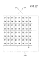
例えば、図22に示すようにC1〜C6カラーフィルタの6バンドのカラーフィルタが配置されたCFA2106aによっても、何れの画素pxにおいてもu方向及びv方向に微分値を算出可能である。また、CFA2106aによれば、本実施形態と同様に、5行5列に並ぶ画素pxによって構成される第2の画素ブロックの中心に配置された単一の画素pxの画素信号のみを出力して画素ブロック毎の微分値を算出することも可能である。
For example, as shown in FIG. 22, the differential value can be calculated in the u direction and the v direction in any pixel px by the
また、図23、図24に示すようにC1〜C6カラーフィルタの6バンドのカラーフィルタが配置されたCFA2107a、2108aによっても、何れの画素pxにおいてもu方向及びv方向に2画素分の間隔で離れた画素pxを用いて微分値を算出可能である。
Also, as shown in FIGS. 23 and 24, the
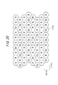
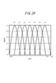
また、例えば、図25に示す分光感度を有するC1〜C7カラーフィルタを用いた、図26に示すCFA2109aであっても、本実施形態と同様の効果が得られる。また、CFA2109aによれば、本実施形態と同様に、5行5列に並ぶ画素pxによって構成される第2の画素ブロックの中心に配置された単一の画素の画素信号のみを出力して画素ブロック毎の微分値を算出することも可能である。
Further, for example, even with the
また、図27〜図29に示す分光感度を有するC1〜C7カラーフィルタをそれぞれ用いた、図30〜32に示すCFA2110a、2111a、2112aによっても、何れの画素pxにおいてもu方向及びv方向に2画素分の間隔で離れた画素を用いて微分値を算出可能である。
Further, the
また、例えば、図33に示す分高感度を有するC1〜C8カラーフィルタを用いた、図34に示すCFA2113aによっても、何れの画素pxにおいてもu方向及びv方向に微分値を算出可能である。また、CFA2113aによれば、本実施形態と同様に、3行3列、5行5列、及び7行7列に並ぶ画素pxによってそれぞれ構成される第1、第2、第3の画素ブロックの中心に配置された単一の画素pxの画素信号のみを出力して画素ブロック毎の微分値を算出することも可能である。
Also, for example, the
また、図35に示す分光感度を有するC1〜C8カラーフィルタを用いた、図36に示すCFA2114aによっても、何れの画素pxにおいてもu方向及びv方向に2画素分の間隔で離れた画素pxを用いて微分値を算出可能である。
In addition, even with the
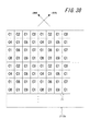
また、例えば、図37に示す分光感度を有するC1〜C9カラーフィルタを用いた、図38に示すCFA2115aによっても、何れの画素pxにおいてもu方向及びv方向に2画素分の間隔で離れた画素pxを用いて微分値を算出可能である。また、CFA2115aによれば、本実施形態と同様に、5行5列に並ぶ画素pxによって構成される第2の画素ブロックの中心に配置された単一の画素pxの画素信号のみを出力して画素ブロック毎の微分値を算出することも可能である。
Further, for example, the
また、例えば、図39、40に示す分光感度を有するC1〜C10カラーフィルタをそれぞれ用いた、図41、42に示すCFA2116a、2117aによっても、何れの画素pxにおいてもu方向及びv方向に2画素分の間隔で離れた画素pxを用いて微分値を算出可能である。なお、CFA2116a、2117aは、8行8列に並ぶ画素によりカラーフィルタ繰返し単位が構成される。また、CFA2116a、2117aによれば、本実施形態と同様に、3行3列に並ぶ画素pxによって構成される第1の画素ブロックの中心に配置された単一の画素pxの画素信号のみを出力して画素ブロック毎の微分値を算出することも可能である。
Further, for example, in any pixel px, two pixels in the u direction and the v direction are obtained by the
また、本実施形態では、通常読出しモードにおいて、全画素信号を用いて微分値を算出する構成であるが、微分値を算出する画素は全画素でなくてもよい。 In the present embodiment, the differential value is calculated using all pixel signals in the normal readout mode. However, the pixels for calculating the differential value may not be all pixels.
例えば、図30に示すCFA2110aにおいては、C1、C2、C4、C6、C7カラーフィルタについてのみ微分値を算出してもよい。CFA2110aにおいては、いずれの画素を注目画素としても、u方向、v方向、行方向、および列方向にそれぞれ注目画素から両側に2画素分離れた2画素のカラーフィルタの種類は同じであり、微分値を算出可能である。しかし、上述の種類のカラーフィルタ(C1、C2、C4、C6、C7)を有する画素を注目画素とする場合には、u方向およびv方向にそれぞれ注目画素から両側に1画素分離れた2画素のカラーフィルタの種類が同じであり、微分値を算出可能である。
For example, in the
また、CFA2110aにおけるC4カラーフィルタのようにサンプル密度が最大である画素の画素信号のみを用いて、微分値を算出してもよい。特に、本実施形態のように、ベイヤー配列のGカラーフィルタと同様に、全体の50%の割合で1種類のカラーフィルタが設けられる構成であれば、全画素から算出した微分値に比べて精度が低下するものの、当該1種類のカラーフィルタの画素信号のみから微分値を算出し、後の信号処理に利用可能である。
Alternatively, the differential value may be calculated using only the pixel signal of the pixel having the maximum sample density, such as the C4 color filter in the
微分値の最適な算出方法は、CFAによって異なっている。図2に示すCFA21aの場合には、いずれの画素を注目画素としても、注目画素に隣接する画素からu方向およびv方向の微分値を算出可能である。さらに、CFA21aの場合には、いずれの画素を注目画素としても、注目画素から行方向および列方向に沿って2画素分離れた2画素から微分値を算出可能である。このように任意のCFAにおいても、複数の方法により微分値を算出可能な場合がある。このようなCFAに対しては、算出された微分値を用いた後の信号処理および処理速度などの観点から最適な微分値算出方法を選択可能である。ただし、注目画素から2画素分離れた画素から算出された微分値よりも、注目画素に隣接する画素から算出された微分値の方が高精度である。さらに、微分値を算出しない画素が存在するよりも全画素位置において微分値が算出される構成の方が好ましい。
The optimum calculation method of the differential value differs depending on the CFA. In the case of the
また、本実施形態では、フレームレートの高速化のために、間引き読出し可能な構成であるが、間引きによる偽像の発生を低下させるために、画素加算して読出してもよい。 In this embodiment, the thinning-out reading is possible in order to increase the frame rate. However, in order to reduce the occurrence of false images due to the thinning-out, pixels may be added and read out.
例えば、本実施形態における第1の間引き読出しモードにおいては、第1の画素ブロックpb1(図3参照)の中心から右上と左下に配置される2画素pxは同じ種類のカラーフィルタを有する。そこで、2画素pxの画素信号を加算させて、第1の画素ブロックpb1の画素信号として出力される。出力される画素信号の色信号成分を第1の画素ブロックpb1のカラーフィルタのバンドとすると、第1の画素ブロックpb1のカラーフィルタの配列は、CFA21aにおけるカラーフィルタの配列と同じである。
For example, in the first decimation readout mode in the present embodiment, the two pixels px arranged at the upper right and lower left from the center of the first pixel block pb1 (see FIG. 3) have the same type of color filter. Therefore, the pixel signals of the two pixels px are added and output as the pixel signal of the first pixel block pb1. If the color signal component of the output pixel signal is the band of the color filter of the first pixel block pb1, the arrangement of the color filters of the first pixel block pb1 is the same as the arrangement of the color filters in the
また、本実施形態における第2の間引き読出しモードにおいては、第2の画素ブロックpb2(図5参照)の中心と4隅とに配置される5画素は同じ種類のカラーフィルタを有する。そこで、5画素の画素信号を加算させて、第2の画素ブロックpb2の画素信号として出力される。出力される画素信号の色信号成分を第2の画素ブロックpb2のカラーフィルタのバンドとすると、第2の画素ブロックpb2のカラーフィルタの配列は、CFA21aにおけるカラーフィルタの配列と同じである。
Further, in the second thinning readout mode in the present embodiment, the five pixels arranged at the center and the four corners of the second pixel block pb2 (see FIG. 5) have the same type of color filter. Therefore, the pixel signals of the five pixels are added and output as the pixel signal of the second pixel block pb2. If the color signal component of the output pixel signal is the band of the color filter of the second pixel block pb2, the arrangement of the color filters of the second pixel block pb2 is the same as the arrangement of the color filters in the
また、本実施形態では、間引き読出しモードでは、3行3列、5行5列、または7行7列に並ぶ画素を画素ブロックとして、間引き読出しをする構成であるが、4行4列の画素によって構成されるカラーフィルタ繰り返し単位に対しては、(2k+3)行(2k+3)列の画素(kは0以上の整数)によって構成される画素ブロック中の所定の位置の単一の画素から画素信号を読出してもよい。このような構成の画素ブロックであれば、CFA21aにおけるカラーフィルタの配列と画素ブロックのカラーフィルタの配列は同じになる。
In the present embodiment, the thinning readout mode is configured to perform thinning readout using pixels arranged in 3 rows, 3 columns, 5 rows, 5 columns, or 7 rows and 7 columns as pixel blocks. Is a pixel signal from a single pixel at a predetermined position in a pixel block composed of pixels of (2k + 3) rows (2k + 3) columns (k is an integer of 0 or more). May be read. In the pixel block having such a configuration, the arrangement of the color filters in the
また、本実施形態では、間引き読出しをするときには、画素ブロックの中心の画素から画素信号を出力させる構成であるが、画素ブロック内の何れの位置の画素から画素信号を出力させてもよい。 In the present embodiment, when thinning readout is performed, a pixel signal is output from the pixel at the center of the pixel block. However, the pixel signal may be output from a pixel at any position in the pixel block.
また、本実施形態では、算出した微分値を適応的カーネル算出部43、NR処理部32、MB−RGB変換処理部33、色変換処理部34、及び色・ガンマ補正処理部35に送信する構成であるが少なくともいずれか一つに送信する構成であってもよいし、微分値に基づいたいかなる処理に用いられてもよい。例えば、エッジ強調処理、局所のコントラスト算出処理、特徴量抽出処理等に用いることも可能である。
In the present embodiment, the calculated differential value is transmitted to the adaptive
10 デジタルカメラ
20 撮像素子
21a、2100a、2101a、2102a、2103a、2104a、2105a、2106a、2107a、2108a、2109a、2110a、2111a、2112a、2113a、2114a、2115a、2116a、2117a カラーフィルタアレイ(CFA)
21u カラーフィルタ繰返し単位
30 画像信号処理部
40 マルチバンドデモザイク(MB)処理部
pb1〜pb3 第1〜第3の画素ブロック
px 画素10
21u color
Claims (15)
前記カラーフィルタアレイにおけるいずれかの種類の前記カラーフィルタによって覆われ、受光量に応じた画素信号を生成する複数の画素を有する撮像素子と、
前記注目カラーフィルタとして前記カラーフィルタアレイ上に配置された種類のカラーフィルタに覆われた画素を1画素ずつ順次注目画素に指定し、前記注目画素から前記第1の方向に沿った両側に前記第1の間隔で配置される2つの前記画素が生成する前記画素信号に基づいて第1の微分情報を算出し、前記注目画素から前記第2の方向に沿った両側に前記第2の間隔で配置される2つの前記画素が生成する前記画素信号に基づいて第2の微分情報を算出する微分情報取得部とを備える
ことを特徴とする撮像装置。Two or more color filters having different spectral sensitivity characteristics, and at least two of the five or more color filters are used as the target color filter, and both sides along the first direction from the target color filter The two color filters arranged at the first interval are of the same type and are arranged at the second interval on both sides along the second direction different from the first direction. A color filter array in which the five or more types of color filters are two-dimensionally arranged so as to be the same type;
An image sensor having a plurality of pixels that are covered by any kind of the color filter in the color filter array and generate a pixel signal according to the amount of received light;
The pixels covered by the color filters of the type arranged on the color filter array as the target color filter are sequentially designated as target pixels one by one, and the first pixel is formed on both sides along the first direction from the target pixel. First differential information is calculated based on the pixel signals generated by the two pixels arranged at an interval of 1, and arranged at the second interval on both sides along the second direction from the target pixel. An imaging apparatus comprising: a differential information acquisition unit that calculates second differential information based on the pixel signals generated by the two pixels that are generated.
前記カラーフィルタはマトリックス状に配置され、
前記第1の方向及び前記第2の方向と行方向との間の角度は45°となり、前記第1の方向及び前記第2の方向と列方向との間の角度は45°となるように構成される
ことを特徴とする撮像装置。The imaging apparatus according to any one of claims 1 to 3,
The color filters are arranged in a matrix,
The angle between the first direction and the second direction and the row direction is 45 °, and the angle between the first direction and the second direction and the column direction is 45 °. An imaging apparatus characterized by comprising.
前記注目カラーフィルタとして配置された前記少なくとも2種類のカラーフィルタの中で2種類のカラーフィルタが隣接しており、
互いに隣接する該2種類のカラーフィルタの一方に覆われた前記画素のみにおいて前記第1の間隔および前記第2の間隔が1画素分の間隔である
ことを特徴とする撮像装置。An imaging apparatus according to any one of claims 1 to 5,
Two types of color filters are adjacent to each other among the at least two types of color filters arranged as the target color filter,
The imaging apparatus, wherein only the pixels covered by one of the two types of color filters adjacent to each other have the first interval and the second interval equal to one pixel.
前記カラーフィルタは、マトリックス状に配置され、
前記5種類以上のカラーフィルタの中の第1のカラーフィルタは、全行及び全列においてそれぞれ、行方向及び列方向に沿って1画素おきに配置される
ことを特徴とする撮像装置。The imaging apparatus according to any one of claims 1 to 3,
The color filters are arranged in a matrix,
The first color filter among the five or more types of color filters is arranged at every other pixel along the row direction and the column direction in all rows and all columns, respectively.
前記注目カラーフィルタから、前記第1の方向および前記第2の方向のなす角を当分割する第3の方向に沿った両側に第3の間隔で配置される2つの前記カラーフィルタは同じ種類のカラーフィルタであり、
前記注目カラーフィルタから、前記第3の方向に垂直な第4の方向に沿った両側に第4の間隔で配置される2つの前記カラーフィルタは同じ種類のカラーフィルタであり、
前記微分情報取得部は、前記注目画素から前記第3の方向に沿った両側に前記第3の間隔で配置される2つの前記画素が生成する前記画素信号に基づいて第3の微分情報を算出し、前記注目画素から前記第4の方向に沿った両側に前記第4の間隔で配置される2つの前記画素が生成する前記画素信号に基づいて第4の微分情報を算出する
ことを特徴とする撮像装置。The imaging device according to any one of claims 1 to 12,
Two color filters arranged at a third interval on both sides along the third direction dividing the angle formed by the first direction and the second direction from the target color filter are of the same type A color filter,
The two color filters arranged at a fourth interval on both sides along a fourth direction perpendicular to the third direction from the target color filter are the same type of color filter,
The differential information acquisition unit calculates third differential information based on the pixel signal generated by the two pixels arranged at the third interval on both sides along the third direction from the target pixel. The fourth differential information is calculated based on the pixel signals generated by the two pixels arranged at the fourth interval on both sides along the fourth direction from the target pixel. An imaging device.
すべての前記画素に前記画素信号を生成させ出力させる通常駆動と、前記通常駆動とは異なる間引き駆動を実行する撮像素子駆動部を備え、
前記撮像素子における複数の前記画素が配置される受光面を分割することにより、包含する前記画素の数が等しい複数の画素ブロックが形成され、
前記撮像素子駆動部は、前記間引き駆動において、前記画素ブロック内の所定の位置の単一の前記画素である間引き画素を覆う前記カラーフィルタを前記画素ブロックのカラーフィルタとみなした全画素ブロックのカラーフィルタの配列が前記カラーフィルタアレイにおける前記カラーフィルタと同じ配列になるように、前記間引き画素を前記撮像素子に出力させ、
前記微分情報取得部は、前記撮像素子が前記間引き駆動を実行する場合に、全前記画素ブロックを注目画素ブロックに指定し、前記注目画素ブロックから前記第1の方向に沿った両側に前記第1の間隔と前記第1の方向に沿った前記画素ブロックの画素数とを乗じた間隔で配置される2つの前記画素ブロックの前記間引き画素が生成する前記画素信号に基づいて第3の微分情報を算出し、前記注目画素ブロックから前記第2の方向に沿った両側に前記第2の間隔と前記第2の方向に沿った前記画素ブロックの画素数とを乗じた間隔で配置される2つの前記画素ブロックの前記間引き画素が生成する前記画素信号に基づいて第4の微分情報を算出する
ことを特徴とする撮像装置。The imaging apparatus according to any one of claims 1 to 13,
An image sensor driving unit that executes normal driving for generating and outputting the pixel signal to all the pixels, and thinning driving different from the normal driving;
By dividing a light receiving surface on which the plurality of pixels in the image sensor are arranged, a plurality of pixel blocks having the same number of the included pixels are formed,
In the thinning driving, the image sensor driving unit considers the color filters that cover the thinned pixels that are single pixels at predetermined positions in the pixel block as color filters of the pixel blocks. The thinned pixels are output to the image sensor so that the filter array is the same array as the color filter in the color filter array,
The differential information acquisition unit designates all the pixel blocks as a target pixel block when the image sensor performs the thinning driving, and the first information on both sides along the first direction from the target pixel block. And the third differential information based on the pixel signal generated by the thinned pixels of the two pixel blocks arranged at an interval obtained by multiplying the interval between the pixel block and the number of pixels of the pixel block along the first direction. Calculated and arranged on both sides along the second direction from the pixel block of interest and arranged at intervals obtained by multiplying the second interval and the number of pixels of the pixel block along the second direction. 4th differential information is calculated based on the said pixel signal which the said thinning pixel of a pixel block produces | generates. The imaging device characterized by the above-mentioned.
Applications Claiming Priority (3)
| Application Number | Priority Date | Filing Date | Title |
|---|---|---|---|
| JP2011106740 | 2011-05-11 | ||
| JP2011106740 | 2011-05-11 | ||
| PCT/JP2012/003068 WO2012153532A1 (en) | 2011-05-11 | 2012-05-10 | Image capture device |
Publications (2)
| Publication Number | Publication Date |
|---|---|
| JPWO2012153532A1 JPWO2012153532A1 (en) | 2014-07-31 |
| JP5943393B2 true JP5943393B2 (en) | 2016-07-05 |
Family
ID=47139019
Family Applications (2)
| Application Number | Title | Priority Date | Filing Date |
|---|---|---|---|
| JP2013513941A Expired - Fee Related JP6074813B2 (en) | 2011-05-11 | 2012-05-10 | Color filter array and image sensor |
| JP2013513940A Active JP5943393B2 (en) | 2011-05-11 | 2012-05-10 | Imaging device |
Family Applications Before (1)
| Application Number | Title | Priority Date | Filing Date |
|---|---|---|---|
| JP2013513941A Expired - Fee Related JP6074813B2 (en) | 2011-05-11 | 2012-05-10 | Color filter array and image sensor |
Country Status (3)
| Country | Link |
|---|---|
| US (2) | US9250121B2 (en) |
| JP (2) | JP6074813B2 (en) |
| WO (2) | WO2012153533A1 (en) |
Families Citing this family (7)
| Publication number | Priority date | Publication date | Assignee | Title |
|---|---|---|---|---|
| JP6200664B2 (en) * | 2013-03-12 | 2017-09-20 | 株式会社Pfu | Image data processing apparatus, image data processing method, and image data processing program |
| WO2015170515A1 (en) * | 2014-05-09 | 2015-11-12 | オリンパス株式会社 | Solid-state imaging element, endoscope, and endoscope system |
| JP6249234B2 (en) * | 2014-10-23 | 2017-12-20 | 京セラドキュメントソリューションズ株式会社 | Image processing device |
| JP7163079B2 (en) * | 2018-06-22 | 2022-10-31 | 株式会社エビデント | Imaging system, image construction method |
| JP7281895B2 (en) * | 2018-12-06 | 2023-05-26 | ソニーセミコンダクタソリューションズ株式会社 | Image sensor and electronic equipment |
| CN116325778A (en) * | 2020-09-25 | 2023-06-23 | 华为技术有限公司 | Compressed image sensor module obtained using pixel rearrangement |
| FR3122930B1 (en) * | 2021-05-11 | 2023-05-26 | Safran Electronics & Defense | Multi-spectral filter |
Citations (6)
| Publication number | Priority date | Publication date | Assignee | Title |
|---|---|---|---|---|
| JP2005286649A (en) * | 2004-03-29 | 2005-10-13 | Sharp Corp | Color filter array and imaging apparatus using it |
| JP2007103401A (en) * | 2005-09-30 | 2007-04-19 | Matsushita Electric Ind Co Ltd | Image pickup device and image processor |
| JP2009284010A (en) * | 2008-05-19 | 2009-12-03 | Canon Inc | Image processor, imaging device, and image processing method |
| JP2009290607A (en) * | 2008-05-29 | 2009-12-10 | Hoya Corp | Imaging apparatus |
| JP2011145448A (en) * | 2010-01-14 | 2011-07-28 | Seiko Epson Corp | Method for manufacturing color filter, color filter, image display device and electronic apparatus |
| JP2011528866A (en) * | 2008-03-28 | 2011-11-24 | ザ トラスティーズ オブ コロンビア ユニヴァーシティ イン ザ シティ オブ ニューヨーク | Universally packed pixel array camera system and method |
Family Cites Families (5)
| Publication number | Priority date | Publication date | Assignee | Title |
|---|---|---|---|---|
| JP2003087806A (en) | 2001-09-12 | 2003-03-20 | Fuji Photo Film Co Ltd | Filter for multi-band camera, its forming method, program for this method, and recording medium with the program recorded |
| US7855740B2 (en) * | 2007-07-20 | 2010-12-21 | Eastman Kodak Company | Multiple component readout of image sensor |
| JP2009100271A (en) * | 2007-10-17 | 2009-05-07 | Olympus Corp | Image pickup device and display device |
| US7745779B2 (en) * | 2008-02-08 | 2010-06-29 | Aptina Imaging Corporation | Color pixel arrays having common color filters for multiple adjacent pixels for use in CMOS imagers |
| US20110149126A1 (en) * | 2009-12-22 | 2011-06-23 | Olympus Corporation | Multiband image pickup method and device |
-
2012
- 2012-05-10 WO PCT/JP2012/003069 patent/WO2012153533A1/en active Application Filing
- 2012-05-10 WO PCT/JP2012/003068 patent/WO2012153532A1/en active Application Filing
- 2012-05-10 JP JP2013513941A patent/JP6074813B2/en not_active Expired - Fee Related
- 2012-05-10 JP JP2013513940A patent/JP5943393B2/en active Active
-
2013
- 2013-10-28 US US14/064,612 patent/US9250121B2/en active Active
- 2013-10-31 US US14/068,151 patent/US9188480B2/en active Active
Patent Citations (6)
| Publication number | Priority date | Publication date | Assignee | Title |
|---|---|---|---|---|
| JP2005286649A (en) * | 2004-03-29 | 2005-10-13 | Sharp Corp | Color filter array and imaging apparatus using it |
| JP2007103401A (en) * | 2005-09-30 | 2007-04-19 | Matsushita Electric Ind Co Ltd | Image pickup device and image processor |
| JP2011528866A (en) * | 2008-03-28 | 2011-11-24 | ザ トラスティーズ オブ コロンビア ユニヴァーシティ イン ザ シティ オブ ニューヨーク | Universally packed pixel array camera system and method |
| JP2009284010A (en) * | 2008-05-19 | 2009-12-03 | Canon Inc | Image processor, imaging device, and image processing method |
| JP2009290607A (en) * | 2008-05-29 | 2009-12-10 | Hoya Corp | Imaging apparatus |
| JP2011145448A (en) * | 2010-01-14 | 2011-07-28 | Seiko Epson Corp | Method for manufacturing color filter, color filter, image display device and electronic apparatus |
Also Published As
| Publication number | Publication date |
|---|---|
| US9188480B2 (en) | 2015-11-17 |
| WO2012153533A1 (en) | 2012-11-15 |
| WO2012153532A1 (en) | 2012-11-15 |
| US20140054448A1 (en) | 2014-02-27 |
| JPWO2012153532A1 (en) | 2014-07-31 |
| US20140118586A1 (en) | 2014-05-01 |
| JP6074813B2 (en) | 2017-02-08 |
| JPWO2012153533A1 (en) | 2014-07-31 |
| US9250121B2 (en) | 2016-02-02 |
Similar Documents
| Publication | Publication Date | Title |
|---|---|---|
| JP5943393B2 (en) | Imaging device | |
| JP6096243B2 (en) | Image data processing method and system | |
| JP5687676B2 (en) | Imaging apparatus and image generation method | |
| JP5872407B2 (en) | Color imaging apparatus and image processing method | |
| US9338364B2 (en) | Imaging device and image generation method | |
| JP2011010108A (en) | Imaging control apparatus, imaging apparatus, and imaging control method | |
| WO2016047240A1 (en) | Image processing device, image pickup element, image pickup device, and image processing method | |
| JP5709131B2 (en) | Image processing system | |
| JP5546166B2 (en) | Imaging apparatus, signal processing method, and program | |
| WO2012124181A1 (en) | Imaging device and imaging program | |
| EP2442556A1 (en) | Apparatus and method for capturing images with high dynamic range | |
| JPWO2017064760A1 (en) | Multilayer imaging device, image processing apparatus, image processing method, and program | |
| JP6230760B1 (en) | Imaging apparatus, image processing apparatus, image processing method, and image processing program | |
| JP5718138B2 (en) | Image signal processing apparatus and program | |
| JP5600812B2 (en) | Imaging device | |
| EP2800373A1 (en) | Color imaging element | |
| JP5738904B2 (en) | Image processing apparatus, imaging apparatus, image processing method, and program | |
| JP5948167B2 (en) | Imaging device | |
| JP2015035782A (en) | Image processing device, imaging device, microscope system, image processing method, and image processing program | |
| JP5912586B2 (en) | Image signal processing method, image signal processing circuit, and imaging apparatus | |
| CN112585960B (en) | Image pickup element, image pickup apparatus, image pickup method, and storage medium | |
| JP2010252089A (en) | Image capturing apparatus and image processing program | |
| JP2008035090A (en) | Signal processing method and camera | |
| JP2012227869A (en) | Image processing device, image processing method and digital camera |
Legal Events
| Date | Code | Title | Description |
|---|---|---|---|
| A621 | Written request for application examination |
Free format text: JAPANESE INTERMEDIATE CODE: A621 Effective date: 20150410 |
|
| A521 | Request for written amendment filed |
Free format text: JAPANESE INTERMEDIATE CODE: A821 Effective date: 20150410 |
|
| TRDD | Decision of grant or rejection written | ||
| A01 | Written decision to grant a patent or to grant a registration (utility model) |
Free format text: JAPANESE INTERMEDIATE CODE: A01 Effective date: 20160510 |
|
| A61 | First payment of annual fees (during grant procedure) |
Free format text: JAPANESE INTERMEDIATE CODE: A61 Effective date: 20160518 |
|
| R150 | Certificate of patent or registration of utility model |
Ref document number: 5943393 Country of ref document: JP Free format text: JAPANESE INTERMEDIATE CODE: R150 |
|
| R250 | Receipt of annual fees |
Free format text: JAPANESE INTERMEDIATE CODE: R250 |
|
| R250 | Receipt of annual fees |
Free format text: JAPANESE INTERMEDIATE CODE: R250 |
|
| R250 | Receipt of annual fees |
Free format text: JAPANESE INTERMEDIATE CODE: R250 |
|
| R250 | Receipt of annual fees |
Free format text: JAPANESE INTERMEDIATE CODE: R250 |
|
| S111 | Request for change of ownership or part of ownership |
Free format text: JAPANESE INTERMEDIATE CODE: R313115 |
|
| R350 | Written notification of registration of transfer |
Free format text: JAPANESE INTERMEDIATE CODE: R350 |
|
| R250 | Receipt of annual fees |
Free format text: JAPANESE INTERMEDIATE CODE: R250 |