JP5936323B2 - Image recording apparatus and control method thereof - Google Patents
Image recording apparatus and control method thereof Download PDFInfo
- Publication number
- JP5936323B2 JP5936323B2 JP2011209002A JP2011209002A JP5936323B2 JP 5936323 B2 JP5936323 B2 JP 5936323B2 JP 2011209002 A JP2011209002 A JP 2011209002A JP 2011209002 A JP2011209002 A JP 2011209002A JP 5936323 B2 JP5936323 B2 JP 5936323B2
- Authority
- JP
- Japan
- Prior art keywords
- image
- period
- vertical transfer
- exposure
- system control
- Prior art date
- Legal status (The legal status is an assumption and is not a legal conclusion. Google has not performed a legal analysis and makes no representation as to the accuracy of the status listed.)
- Expired - Fee Related
Links
Images


Classifications
-
- H—ELECTRICITY
- H04—ELECTRIC COMMUNICATION TECHNIQUE
- H04N—PICTORIAL COMMUNICATION, e.g. TELEVISION
- H04N7/00—Television systems
-
- H—ELECTRICITY
- H04—ELECTRIC COMMUNICATION TECHNIQUE
- H04N—PICTORIAL COMMUNICATION, e.g. TELEVISION
- H04N23/00—Cameras or camera modules comprising electronic image sensors; Control thereof
- H04N23/80—Camera processing pipelines; Components thereof
-
- H—ELECTRICITY
- H04—ELECTRIC COMMUNICATION TECHNIQUE
- H04N—PICTORIAL COMMUNICATION, e.g. TELEVISION
- H04N23/00—Cameras or camera modules comprising electronic image sensors; Control thereof
- H04N23/70—Circuitry for compensating brightness variation in the scene
- H04N23/741—Circuitry for compensating brightness variation in the scene by increasing the dynamic range of the image compared to the dynamic range of the electronic image sensors
Description
本発明は、動画像を記録する画像記録装置およびその制御方法に関する。 The present invention relates to an image recording apparatus and a control how to record a moving image.
近年、デジタルカメラなどの画像記録装置においては、音声付き動画像を撮影記録する機能が備えられている。このような画像記録装置では、動画像を撮影記録する際、撮像素子におけるフレームレート、つまり、撮影時のフレームレートを記録フレームレートとして動画像の記録を行っている。 In recent years, an image recording apparatus such as a digital camera has a function of shooting and recording a moving image with sound. In such an image recording apparatus, when a moving image is shot and recorded, the moving image is recorded using the frame rate of the image sensor, that is, the frame rate at the time of shooting, as the recording frame rate.
さらには、高いフレームレートで撮像した動画像を低いフレームレートで記録して決定的な瞬間をスロー再生する機能も備えられている。また、複数の撮像素子の出力を合成して記録するようにした画像記録装置もある。 Furthermore, a function of recording a moving image captured at a high frame rate at a low frame rate and slow-playing a decisive moment is also provided. There is also an image recording apparatus in which outputs from a plurality of image sensors are combined and recorded.
例えば、画像記録装置において、互いに蓄積期間を変更して複数の撮像素子から出力される出力画像信号を1つの画像信号を合成して、ダイナミックレンジの広い動画像を得るようにしたものがある(特許文献1参照)。 For example, in an image recording apparatus, a moving image having a wide dynamic range is obtained by synthesizing one image signal with output image signals output from a plurality of image sensors while changing the accumulation period. Patent Document 1).
ところが、特許文献1に記載の画像記録装置では、撮像フレームレートによって撮像装置における蓄積時間が限定される。このため、低照度における撮像画像が期待よりも暗く、所望のダイナミックレンジが得られないことがある。
However, in the image recording apparatus described in
さらに、ダイナミックレンジを広くするため、撮像画像にゲインを乗算すると撮影画像においてノイズが強調されてしまうことがある。 Furthermore, when the captured image is multiplied by a gain in order to widen the dynamic range, noise may be emphasized in the captured image.
従って、本発明の目的は、ダイナミックレンジの広い動画像を得る際に、低照度環境下においてもノイズの少ない動画像を得ることのできる画像記録装置およびその制御方法を提供することにある。 Accordingly, an object of the present invention, in obtaining a wide dynamic image dynamic range, to provide an image recording apparatus and a control how can be obtained with less moving image noise even in low light environments.
上記目的を達成するために、本発明による画像記録装置は、異なる露出レベルで被写体を撮像することにより電荷を蓄積し、前記蓄積された電荷を複数の画像信号として出力する撮像手段と、前記撮像手段から出力される複数の画像信号を合成して合成画像を得る画像合成手段と、所定のフレームレートで前記合成画像をメモリに記録する記録手段と、前記撮像手段から前記複数の画像信号を読み出す際のそれぞれの垂直転送期間を前記異なる露出レベルに応じて異ならせて、前記垂直転送期間の合計を前記所定のフレームレートで規定される時間に制御する制御手段とを有し、前記制御手段は、直前のフレーム期間で撮像された画像における被写界輝度に応じて前記垂直転送期間を変化させることを特徴とする。 To achieve the above object, an image recording apparatus according to the present invention accumulates charges by imaging a subject at different exposure levels, and outputs the accumulated charges as a plurality of image signals, and the imaging Image synthesizing means for synthesizing a plurality of image signals output from the means, obtaining a synthesized image, recording means for recording the synthesized image in a memory at a predetermined frame rate, and reading the plurality of image signals from the imaging means Control means for controlling the total of the vertical transfer periods to a time defined by the predetermined frame rate by varying each vertical transfer period according to the different exposure level. The vertical transfer period is changed according to the field luminance in the image captured in the immediately preceding frame period .
本発明による画像記録装置の制御方法は、異なる露出レベルで被写体を撮像することにより電荷を蓄積し、前記蓄積された電荷を複数の画像信号として出力する撮像手段を備える画像記録装置の制御方法であって、前記撮像手段から出力される複数の画像信号を合成して合成画像を得る画像合成ステップと、所定のフレームレートで前記合成画像をメモリに記録する記録ステップと、前記撮像手段から前記複数の画像信号を読み出す際のそれぞれの垂直転送期間を前記異なる露出レベルに応じて異ならせて、前記垂直転送期間の合計を前記所定のフレームレートで規定される時間に制御する制御ステップとを有し、前記制御ステップは、直前のフレーム期間で撮像された画像における被写界輝度に応じて前記垂直転送期間を変化させることを特徴とする。 An image recording apparatus control method according to the present invention is a method for controlling an image recording apparatus comprising an imaging unit that accumulates charges by imaging a subject at different exposure levels and outputs the accumulated charges as a plurality of image signals. An image synthesis step of synthesizing a plurality of image signals output from the imaging means to obtain a synthesized image; a recording step of recording the synthesized image in a memory at a predetermined frame rate; A control step of controlling the total of the vertical transfer periods to a time defined by the predetermined frame rate by varying each vertical transfer period when reading the image signal of the image signal according to the different exposure levels. the controlling step, altering the vertical transfer period in accordance with the field brightness in the captured image frame period immediately before And butterflies.
本発明によれば、垂直転送期間を有効に露光時間に割り当てることができ、複数の画像に露出時間差がつくため、ダイナミックレンジ拡大を行うことができる。 According to the present invention , the vertical transfer period can be effectively allocated to the exposure time, and the exposure time difference is added to a plurality of images, so that the dynamic range can be expanded .
以下、本発明の実施の形態による画像記録装置について図面を参照して説明する。 Hereinafter, an image recording apparatus according to an embodiment of the present invention will be described with reference to the drawings.
[第1の実施形態]
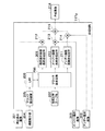
図1は、本発明の第1の実施形態による画像記録装置が用いられた撮像装置の一例を示すブロック図である。
[First Embodiment]
FIG. 1 is a block diagram showing an example of an imaging apparatus using the image recording apparatus according to the first embodiment of the present invention.
図1において、図示の撮像装置は、例えば、デジタルカメラ(以下単にカメラと呼ぶ)100であり、ズームレンズ110を備えている。ズームレンズ110の後段にはブレを補正するためのシフトレンズ111、焦点調節用フォーカスレンズ112、メカニカルシャッタ113、および絞り114が配置されている。絞り114を通過した被写体の光学像は固体撮像素子(以下単に撮像素子と呼ぶ)115(例えば、CCD)に結像する。
In FIG. 1, the illustrated imaging apparatus is, for example, a digital camera (hereinafter simply referred to as a camera) 100 and includes a
この撮像素子115は2次元マットリックス状に配列された複数の画素を有している。つまり、撮像素子115は行方向および列方向に配列された複数の画素を有している。撮像素子115はタイミング発生部116から出力されるタイミングパルスによって駆動されて、光学像に応じた電気信号(アナログ信号)を出力する。そして、このアナログ信号は画像処理部117に与えられる。
The
画像処理部117は、前処理回路117a、SSG回路(水平垂直同期信号発生回路)117b、AF評価値演算回路117c、信号処理回路117d、輝度積分回路117e、縮小回路117f、画像合成回路117g、ラスターブロック変換回路117h、および圧縮回路117iを備えている。
The
SSG回路117bはタイミング発生部116から撮像駆動用クロック信号を受けて、水平および垂直同期信号をタイミング発生部116および撮像素子115に与える。
The
前処理回路117aは撮像素子115からの出力であるアナログ信号をデジタル信号(画像信号とも呼ぶ)に変換して、行単位で画像信号を輝度積分回路117eおよび信号処理回路117dに分配する。さらに、前処理回路117aはチャネル間のデータ補正などの処理も行う。
The preprocessing circuit 117a converts an analog signal output from the
AF評価値演算回路117cは、予め設定された複数の評価領域において画像信号の輝度成分に対して水平方向のフィルタ処理を施す。そして、AF評価値演算回路117cはコントラストを示す所定周波数を抽出しつつコントラストの最大値を選択して、垂直方向に積分演算を行う。
The AF evaluation
輝度積分回路117eは、RGB(赤・緑・青)信号から輝度成分を混合生成して、画像信号を複数の領域に分割する。そして、輝度積分回路117eは分割領域毎に輝度成分を生成する。
The
信号処理回路117dは、画像信号に対して色キャリア除去、アパーチャー補正、およびガンマ補正処理などを行って輝度信号を生成する。さらに、信号処理回路117dは画像信号に対して色補間、マトリックス変換、ガンマ処理、およびゲイン調整などを行って色差信号を生成する。そして、信号処理回路117dはメモリ部123にYUV形式の画像データを記録する。
The
なお、Yは輝度信号を表し、Uは輝度信号と青色成分との差を表す。そして、Vは輝度信号と赤色成分との差を表す。また、信号処理回路117dは、YUV形式の画像データにおいて輝度信号(Y)をレベル毎に集計して、画像データ毎に輝度分布データを生成する。
Y represents the luminance signal, and U represents the difference between the luminance signal and the blue component. V represents the difference between the luminance signal and the red component. In addition, the
画像合成回路117gは、メモリ部123に記録された画像データ又は信号処理回路で生成された複数のYUV形式の画像データに、画素単位で設定された係数を乗じた後加算して、合成画像データを生成する。なお、画像合成回路117gにおける合成処理については後ほど詳細に説明する。
The
縮小回路117fは、信号処理回路から画像データを受け、画素データの切り出し、間引き、および線形補間処理などを行って、水平垂直方向に画素データの縮小処理を行う。ラスターブロック変換回路117hは、縮小回路117fにおいて変倍されたラスタースキャン画像データをブロックスキャン画像データに変換する。
The
上記の一連の画像処理においては、メモリ部123がバッファメモリとして用いられ、圧縮回路117iはブロックスキャンデータに変換したYUV画像データを動画圧縮方式に従って圧縮して、動画ビットストリームとして出力する。
In the above series of image processing, the
カメラ100は露出制御部118を備えている。露出制御部118はメカニカルシャッタ113および絞り114を制御する露出制御部である。レンズ制御部119はズームレンズ110および焦点調節レンズ112を光軸に沿って移動させ、光学像を撮像素子115に結像させる。
The
また、レンズ制御部119は角速度センサおよび加速度センサ(図示せず)の出力に応じてシフトレンズ111を駆動して手ブレを光学的に補正する。
In addition, the
システム制御回路121にはレリーズスイッチ120が接続され、レリーズスイッチ120の操作によってシステム制御回路121に撮影指示が行われる。マイクロフォン(マイク)127によって入力音声が音声信号に変換され、この音声信号はA/D変換器128によってデジタル音声信号に変換される。そして、このデジタル音声信号は音声処理部129によって所定の音声処理が施された後、音声ビットストリームとしてシステム制御回路121に与えられる。
A release switch 120 is connected to the
システム制御回路121はカメラ100全体の制御を司る。システム制御回路212は、例えば、CPU、インターフェイス回路、DMAC(Direct・Memory・Access・Controller)、およびバスアービターなどを有しており、CPUはフラッシュメモリ122に記憶された制御プログラムを実行する。
A
電池ボックス140には電池142が収納され、電池142は接続端子130および141によってカメラ100に結合されている。記録媒体収納部131には記録媒体133が収納される。記録媒体133には画像データが記録され、記録媒体133は接続端子125および132によってカメラ100に接続される。
A
システム制御回路121には媒体記録禁止検知スイッチ134および記録媒体着脱検知スイッチ126が接続されている。媒体記録禁止検知スイッチ134によって記録媒体134に対する書き込み禁止が検知されると、システム制御回路121は記録媒体133に対する画像データの記録を禁止する。
A medium recording
また、記録媒体着脱検知スイッチ126によって、システム制御回路121は記録媒体133の着脱を知る。ここでは、記録媒体収納部131から記録媒体133が取り外されると、記録媒体着脱検知スイッチ126はオフする。
Further, the
一方、記録媒体収納部131から記録媒体133に挿入されると、記録媒体着脱検知スイッチ126はオンする。なお、動画記録スイッチ180によってシステム制御回路121に対して動画記録が指示される。
On the other hand, when the
再生回路150はメモリ部123に記憶された画像データを表示用画像データに変換して、表示用画像としてモニタ(表示装置)151に転送する。そして、モニタ151に表示用画像が表示される。
The
再生回路150は、YUV形式の画像データを輝度信号Yと変調色差成分Cとに分離した後、輝度信号YをD/A変換する。そして、アナログ輝度信号に対してローパスフィルタ処理(LPF処理)を施す。
The
さらに、再生回路150は変調色差成分Cに対して、D/A変換を行って、アナログ変調色差成分に対してバンドパスフィルタ処理(BPF処理)を施して、周波数成分のみを抽出する。そして、再生回路150は信号成分とサブキャリア周波数とに基づいて、輝度信号YおよびRGB信号を生成して、表示用画像データとしてモニタ151に出力する。
Further, the
このようにして、再生回路150によって画像データを逐次処理してモニタ151に表示するようにすれば、モニタ151を電子ビューファインダー(EVF)として用いることができる。
In this way, if image data is sequentially processed by the
図2は、図1に示す画像合成回路における画像合成処理を説明するための図である。 FIG. 2 is a view for explaining image composition processing in the image composition circuit shown in FIG.
画像合成回路117gには、画像データとして適正露出画像データ201、アンダー露出画像データ202、およびオーバー露出画像データ203が入力される。なお、以下の説明では画像データを単に画像と呼ぶことがある。
The
ここで、適正露出画像とは撮影環境下において適正な露出で撮影して得られた画像をいう。アンダー露出画像とは適正な露出よりも低い露出で撮影して得られた画像をいう。また、オーバー露出画像とは適正な露出よりも高い露出で撮影して得られた画像をいう。 Here, the proper exposure image means an image obtained by photographing with proper exposure under a photographing environment. An under-exposed image is an image obtained by photographing at an exposure lower than the proper exposure. An overexposed image refers to an image obtained by photographing at an exposure higher than the proper exposure.
さらに、画像合成回路117gには、輝度積分回路117eにおいて適正露出画像について領域(以下ブロックともいう)毎に生成された輝度成分を積分した輝度積分値204がブロック積分結果205として与えられる。そして、画像合成回路117gは、ブロック積分結果205について水平・垂直方向に対してLPF処理206を施して、LPFデータとする。
Further, the
合成比率テーブル207には、適正露出画像、アンダー露出画像、およびオーバー露出画像の合成比率を示す合成比率係数が格納されている。 The combination ratio table 207 stores a combination ratio coefficient indicating a combination ratio of a properly exposed image, an underexposed image, and an overexposed image.
図3は、図2に示す合成比率テーブルの一例を示す図である。 FIG. 3 is a diagram showing an example of the synthesis ratio table shown in FIG.
図3に示すように、合成比率テーブルには、輝度レベルに対応して、適正露出画像比率(適正比率)、アンダー露出画像比率(アンダー比率)、およびオーバー露出画像比率(オーバー比率)が係数として定められている。図示の例では、適正露出画像、アンダー露出画像、およびオーバー露出画像についてその画素単位の比率合計が1となるように比率が設定される。 As shown in FIG. 3, in the synthesis ratio table, the appropriate exposure image ratio (appropriate ratio), underexposure image ratio (under ratio), and overexposure image ratio (over ratio) are used as coefficients corresponding to the luminance level. It has been established. In the example shown in the figure, the ratio is set so that the total ratio of the pixel units of the properly exposed image, the underexposed image, and the overexposed image is 1.
なお、被写界輝度(被写体輝度)に応じて画素単位の比率合計が1を超えるように各比率を設定するようにしてもよい。 Each ratio may be set so that the total ratio of the pixel unit exceeds 1 according to the field luminance (subject luminance).
画像合成回路117gはLPFデータに対してブロック画素変換処理208を行う。ここでは、画像合成回路117gはLPFデータにおける輝度値レベルに応じて合成比率テーブルを参照して、それぞれ適正露出画像、アンダー露出画像、およびオーバー露出画像の比率(つまり。係数)を画素単位で決定する。
The
そして、画像合成回路117gは適正露出画像画素合成比率209、オーバー露出画像画素合成比率210、およびアンダー露出画像画素合成比率211を得る。
Then, the
図示の例では、オーバー露出は適正露出よりも露出が1.5段高い露出であり、アンダー露出は適正露出よりも1.5段低い露出である。 In the illustrated example, overexposure is exposure that is 1.5 steps higher than appropriate exposure, and underexposure is exposure that is 1.5 steps lower than proper exposure.
続いて、画像合成回路117gは乗算器212によって適正露出画像画素合成比率209を画素単位で適正露出画像201に乗算して、補正適正露出画像とする。同様に、画像合成回路117gは乗算器213によってオーバー露出画像画素合成比率210を画素単位でオーバー露出画像203に乗算して、補正オーバー露出画像とする。
Subsequently, the
また、画像合成回路117gは乗算器214によってアンダー露出画像画素合成比率211を画素単位でアンダー露出画像202に乗算して、補正アンダー露出画像とする。
Also, the
次に、画像合成回路117gは加算器215で補正適正露出画像、補正オーバー露出画像、および補正アンダー露出画像を加算して、合成画像216として出力する。
Next, the
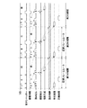
図4は、図1に示すカメラ100における画像合成処理のタイミングを説明するための図である。
FIG. 4 is a diagram for explaining the timing of image composition processing in the
図4に示す例では、撮像素子115を駆動するための最短の垂直期間(垂直転送期間)を撮像素子115の読み出し速度によって決定する。そして、撮像素子115の読み出し速度は動画像の記録フレームレートより充分に短いものとする。
In the example illustrated in FIG. 4, the shortest vertical period (vertical transfer period) for driving the
ここでは、撮像素子115のダイナミックレンジを拡張するため、撮像駆動における垂直期間として第1〜第3の垂直期間I〜IIIを設定する。そして、第1〜第3の垂直期間I〜IIIの各々を一単位として周期的に撮像素子115を駆動する。この際、第1〜第3の垂直期間I〜IIIの合計が動画像の記録フレームレートに設定される。
Here, in order to extend the dynamic range of the
第1〜第3の垂直期間I〜IIIの各々における最大蓄積時間はそれぞれその垂直期間にほぼ相当する。これによって、第1〜第3の垂直期間I〜IIIが異なれば、互いに蓄積時間の異なる画像が得られることになる。なお、ここでは垂直期間とは撮像素子115の列方向における走査期間をいう。
The maximum accumulation time in each of the first to third vertical periods I to III substantially corresponds to the vertical period. Thus, if the first to third vertical periods I to III are different, images having different accumulation times can be obtained. Here, the vertical period refers to a scanning period in the column direction of the
図4において、垂直同期信号VDに応じて、電子シャッターを動作させる。ここでは、第1の垂直期間Iに対応する蓄積時間(電荷蓄積時間)を第1の蓄積時間Iとし、第2の垂直期間IIに対応する蓄積時間を第2の蓄積時間IIとする。また、第3の垂直期間IIIに対応する蓄積時間を第3の蓄積時間IIIとする。 In FIG. 4, the electronic shutter is operated in accordance with the vertical synchronization signal VD. Here, the accumulation time (charge accumulation time) corresponding to the first vertical period I is defined as the first accumulation time I, and the accumulation time corresponding to the second vertical period II is defined as the second accumulation time II. Further, the accumulation time corresponding to the third vertical period III is defined as a third accumulation time III.
なお、I<II<IIIである。また、最大蓄積時間よりも短い蓄積時間については電子シャッターによって撮像素子115に蓄積された電荷の掃き捨てを行う。
Note that I <II <III. For the storage time shorter than the maximum storage time, the charge stored in the
まず、第1の期間(記憶フレームレート)において、蓄積時間が最小の第1の垂直期間Iでは、被写界(被写体)の明部が適正露出に近づくように露出(つまり、露光時間)が制御される。蓄積時間が中間の第2の垂直期間IIでは、被写界が適正露出になるように露出が制御される。そして、蓄積時間が最大の第3の垂直期間IIIでは、被写界の暗部が適正露出に近づくように露出が制御される。このように、垂直期間を露光時間毎に異ならせる。 First, in the first period (memory frame rate), in the first vertical period I with the shortest accumulation time, the exposure (that is, the exposure time) is such that the bright part of the object scene (subject) approaches the appropriate exposure. Be controlled. In the second vertical period II where the accumulation time is intermediate, the exposure is controlled so that the object scene has an appropriate exposure. In the third vertical period III in which the accumulation time is maximum, the exposure is controlled so that the dark part of the object scene approaches the appropriate exposure. In this way, the vertical period is varied for each exposure time.
第1〜第3の垂直期間I〜IIIで撮像素子115に蓄積された電荷(蓄積電荷)は次の垂直期間で画像信号(アナログ信号)として読み出される。そして、撮像素子115から読み出されたアンダー露出画像および適正露出画像は、前述のようにして、信号処理回路117dでYUV信号に変換されてメモリ部123に記憶される。
Charges (accumulated charges) accumulated in the
一方、輝度積分回路117eは、第2の垂直期間IIで読み出された適正露出画像を読み込んで、前述のようにしてブロック積分結果Aを生成する。従って、第3の垂直期間IIIにおいては、適正露出画像をメモリ部123に書き込む処理と輝度積分回路117eにおける輝度積分処理とが行われることになる。
On the other hand, the
そして、ブロック積分結果Aに応じて次の露出制御値の算出が行われるとともに、前述のように合成形成の決定が行われる(係数生成)。 Then, the next exposure control value is calculated according to the block integration result A, and the composite formation is determined as described above (coefficient generation).
合成係数が決定されると、第3の垂直期間IIIにおいて蓄積されたオーバー露出画像が、第2の期間における第1の垂直期間Iで読み出される。第2の期間における第1の垂直期間Iにおいて、信号処理回路117dはYUV形式の画像データに変換されたオーバー露出画像の入力に同期して、メモリ部123に記憶したアンダー露出画像および適正露出画像を読み出して画像合成回路11gに与える。
When the synthesis coefficient is determined, the overexposed image accumulated in the third vertical period III is read out in the first vertical period I in the second period. In the first vertical period I in the second period, the
そして、画像合成回路117gは第2の期間において画素毎に同期を取って、前述したようにして、合成画像を出力する。その後、圧縮回路117iにおいて圧縮処理が行われる。このようにして、第1〜第3の期間の各々を1つの記憶フレームレートとして画像合成が順次行われることになる。
Then, the
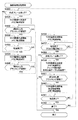
図5は、図1に示すカメラ100で行われる動画撮影処理の一例を説明するためのフローチャートである。なお、図5に示すフローチャートはシステム制御回路121および画像処理部117によって行われる。
FIG. 5 is a flowchart for explaining an example of the moving image shooting process performed by the
図1および図5を参照して、システム制御回路121は、図4で説明した撮像駆動および露光制御を行うため撮像駆動処理を起動する(ステップS400)。続いて、システム制御回路121は適正露出画像の輝度積分結果に基づいて、第1〜第3の蓄積時間I〜IIIを決定して露出制御を起動する(ステップS401)。そして、システム制御回路121は、適正露出画像、アンダー露出画像、およびオーバー露出画像を周期的に合成するための画像合成処理を起動する(ステップS402)。
Referring to FIGS. 1 and 5, the
撮像駆動処理、露出制御、および画像合成処理を起動した後、システム制御回路121は動画記録スイッチ180がオンされて動画像の記録指示(動画記録指示)があったか否かを判定する(ステップS403)。動画記録指示がないと(ステップS403において、NO)、システム制御回路121は待機する。
After starting the imaging drive process, the exposure control, and the image composition process, the
一方、動画記録指示があると(ステップS403において、YES)、画像処理部117はシステム制御回路121の制御下で、前述のように合成画像をエンコードしてメモリ部123に蓄積するととともに記録媒体133に記録する画像記録処理を行う(ステップS404)。
On the other hand, when there is a moving image recording instruction (YES in step S403), the
続いて、システム制御回路121は動画記録停止指示があったか否かを判定する(ステップS405)。動画記録停止指示がないと(ステップS405において、NO)、システム制御回路121は待機する。
Subsequently, the
動画記録停止指示があると(ステップS405において、YES)、続いて、システム制御回路121は動画撮影の終了であるか否かを判定する(ステップS406)。動画撮影の終了でないと(ステップS406において、NO)、システム制御回路121はステップS403の処理に戻る。
If there is an instruction to stop moving image recording (YES in step S405), then
動画像撮影の終了であると(ステップS406において、YES)、システム制御回路121は終了処理を行って(S407)、動画撮影処理を終了する。
If it is the end of moving image shooting (YES in step S406), the
図6は、図5に示す撮像駆動処理を説明するためのフローチャートである。 FIG. 6 is a flowchart for explaining the imaging drive process shown in FIG.
図1および図6を参照して、まず、システム制御回路121はアンダー露出画像を蓄積する期間(蓄積期間)の駆動設定(アンダー駆動設定)を行う。この際、システム制御回路121は当該蓄積期間に対応する垂直期間(垂直転送期間)において、後述する露出制御で決定した露出がアンダーとなる時間(アンダー露光時間)の設定を行う(ステップS410)。
Referring to FIGS. 1 and 6, first,
ステップS410の設定によって、画像処理部117のSSG回路117bから出力される水平垂直同期信号が切り替わって、撮像素子115の蓄積時間の設定が切り替わる。システム制御回路121は上記の切り替わりが行われたか否かを判定する(ステップS411)。切り替わりが終了しないと(ステップS411において、NO)、システム制御回路121は待機する。
With the setting in step S410, the horizontal / vertical synchronization signal output from the
一方、切り替わりが終了すると(ステップS411において、YES)、システム制御回路121は露出制御部118を制御してその垂直転送期間で、設定アンダー露光が得られる蓄積時間で露光を行う。この際、前の垂直転送期間で蓄積したオーバー露出画像が撮像素子115から読み出される。
On the other hand, when the switching is completed (YES in step S411), the
続いて、システム制御回路121は適正露出画像を蓄積する蓄積期間の駆動設定(適正駆動設定)を行う。この際、システム制御回路121は当該蓄積期間に対応する垂直転送期間において露出制御で決定した露出が適正となる時間(適正露光時間)の設定を行う(ステップS412)。
Subsequently, the
ステップS412の設定によって、画像処理部117のSSG回路117bから出力される水平垂直同期信号が切り替わって、撮像素子115の蓄積時間の設定が切り替わる。システム制御回路121は上記の切り替わりが行われたか否かを判定する(ステップS413)。切り替わりが終了しないと(ステップS413において、NO)、システム制御回路121は待機する。
With the setting in step S412, the horizontal / vertical synchronization signal output from the
一方、切り替わりが終了すると(ステップS413において、YES)、システム制御回路121は露出制御部118を制御してその垂直転送期間で、設定適正露光が得られる蓄積時間で露光を行う。この際、前の垂直転送期間で蓄積したアンダー露出画像が撮像素子115から読み出される。
On the other hand, when the switching is completed (YES in step S413), the
次に、システム制御回路121は撮像駆動処理が終了であるか否かを確認する(ステップS414)。撮像駆動処理が終了であれば(ステップS414において、YES)、システム制御回路121は駆動終了処理を行って(ステップS415)、撮像駆動処理を終了する。
Next, the
撮像駆動処理が終了でないと(ステップS414において、NO)、システム制御回路121はオーバー露出画像を蓄積する蓄積期間の駆動設定(オーバー駆動設定)を行う。この際、システム制御回路121は当該蓄積期間に対応する垂直転送期間において露出制御で決定した露出がオーバーとなる時間(オーバー露光時間)と輝度積分の設定を行う(ステップS416)。
If the imaging drive process has not ended (NO in step S414), the
ステップS416の設定によって、画像処理部117のSSG回路117bから出力される水平垂直同期信号が切り替わって、撮像素子115の蓄積時間の設定が切り替わる。システム制御回路121は上記の切り替わりが行われたか否かを判定する(ステップS417)。切り替わりが終了しないと(ステップS417において、NO)、システム制御回路121は待機する。
With the setting in step S416, the horizontal / vertical synchronization signal output from the
一方、切り替わりが終了すると(ステップS417において、YES)、システム制御回路121は露出制御部118を制御してその垂直転送期間で、設定オーバー露光が得られる蓄積時間で露光を行う。
On the other hand, when the switching is completed (YES in step S417), the
この際、前の垂直転送期間で蓄積した適正露出画像が撮像素子115から読み出される。そして、画像処理部117の輝度積分回路117eにおいて、当該適正露出画像に対して輝度積分が行われる。システム制御回路121はステップS410の処理に戻る。
At this time, the proper exposure image accumulated in the previous vertical transfer period is read from the
このようにして一連の処理が周期的に行われて、アンダー露出画像、適正露出画像、およびオーバー露出画像が撮像素子115から出力される。なお、アンダー露出画像、適正露出画像、オーバー露出画像の読み出し順序は、撮像素子115の特性などに合わせて決定され、必ずしも図6に示す読み出し順序に限定されるものではない。
In this way, a series of processes are periodically performed, and an underexposure image, a proper exposure image, and an overexposure image are output from the
図7は、図5に示す露出制御処理を説明するためのフローチャートである。 FIG. 7 is a flowchart for explaining the exposure control process shown in FIG.
図1および図7を参照して、露出制御の基準となる被写界輝度に係る測光用輝度積分については、前述の撮像駆動処理で説明したタイミングで適正露出画像に対して行われる。 With reference to FIG. 1 and FIG. 7, the photometric luminance integration relating to the field luminance, which is a reference for exposure control, is performed on the appropriate exposure image at the timing described in the above-described imaging drive processing.
まず、システム制御回路121は輝度積分(ブロック積分)が終了したか否かを判定する(ステップS420)。輝度積分が終了しないと(ステップS420において、NO)、システム制御回路121は待機する。
First, the
輝度積分が終了すると(ステップS420において、YES)、システム制御回路121は輝度積分結果と前回の適正露出画像を蓄積した際の露出制御値とに基づいて、被写界輝度値を求める(ステップS421)。
When the luminance integration is completed (YES in step S420), the
そして、システム制御回路121は被写界輝度値に基づいて適正露出が得られる露出制御値を求めるとともに、アンダー露出画像およびオーバー露出画像が得られる露出制御値を求める(ステップS422)。
Then, the
続いて、システム制御回路212は、次の記録フレームレートにおいて適正露出制御値とアンダー露出画像およびオーバー露出画像を得る露出制御値とに応じた蓄積時間の設定に係る制御要求を行う(ステップS423)。そして、システム制御回路121は露出制御処理が終了したか否かを判定する(ステップS424)。
Subsequently, the
露出制御処理が終了しないと判定すると(ステップS424において、NO)、システム制御回路121はステップS420の処理に戻る。一方、露出制御処理が終了したと判定すると(ステップS424において、YES)、システム制御回路121は露出制御処理を終了する。
If it is determined that the exposure control process is not completed (NO in step S424),
なお、露出制御処理においては、露出の変化が激しくならないようにするため、輝度積分結果又は露出制御値を周期的に間引くようにしてもよい。 In the exposure control process, the luminance integration result or the exposure control value may be periodically thinned out so that the change in exposure does not become severe.
図8は、図5に示す画像合成処理を説明するためのフローチャートである。 FIG. 8 is a flowchart for explaining the image composition processing shown in FIG.
図1および図8を参照して、画像合成処理が開始されると、システム制御回路121は画像処理部117に対してYUV画像を生成する設定を行うともに、画像処理部117で得られたYUV画像をメモリ部123に転送する設定を行う(ステップS430)。
Referring to FIGS. 1 and 8, when the image synthesis process is started, the
設定の後、システム制御回路121はアンダー露出画像が読み出される垂直転送期間直前のブランキング(非映像)期間であるか否かを判定する(ステップS431)。
After the setting, the
ブランキング期間でないと(ステップS431において、NO)、システム制御回路121は待機する。一方、ブランキング期間であると(ステップS431において、YES)、システム制御回路121はブランキング期間においてYUV画像の生成開始を設定するとともに、YUV画像転送許可設定を行う(ステップS432)。
If it is not the blanking period (NO in step S431), the
これによって、アンダー露出画像が読み出されると、画像処理部117においてYUV画像の生成が開始され、順次YUV画像がメモリ部123に転送される。
Thus, when the underexposed image is read, the
システム制御回路121はアンダー露出画像(YUV画像)の転送が完了したか否かを監視する(ステップS433)。アンダー露出画像の転送が完了しない場合には(ステップS433において、NO)、システム制御回路121は待機する。
The
アンダー露出画像の転送が完了すると(ステップS433において、YES)、システム制御回路121は、画像処理部117に対して次のYUV画像を生成する設定を行うとともに、画像処理部117で生成されたYUV画像をメモリ部123に転送する設定を行う(ステップS434)。
When the transfer of the underexposed image is completed (YES in step S433), the
設定の後、システム制御回路121は適正露出画像が読み出される垂直転送期間直前のブランキング(非映像)期間であるか否かを判定する(ステップS435)。ブランキング期間でないと(ステップS435において、NO)、システム制御回路121は待機する。
After the setting, the
一方、ブランキング期間であると(ステップS435において、YES)、システム制御回路121はブランキング期間においてYUV画像の生成開始を設定するとともに、YUV画像転送許可設定を行う(ステップS436)。
On the other hand, if it is the blanking period (YES in step S435), the
これによって、適正露出画像が撮像素子115から読み出されると、画像処理部117においてYUV画像の生成が開始され、順次YUV画像がメモリ部123に転送される。
As a result, when a proper exposure image is read from the
システム制御回路121は適正露出画像(YUV画像)の転送が完了するとともにブロック積分が完了したか否かを監視する(ステップS437)。適正露出画像の転送が完了しないと(ステップS437において、NO)、システム制御回路121は待機する。
The
適正露出画像の転送が完了すると(ステップS437において、YES)、システム制御回路121は、画像処理部117に対して次のYUV画像を生成する設定を行うとともに、画像処理部117で生成されたYUV画像をメモリ部123に転送する設定を行う。
When the transfer of the proper exposure image is completed (YES in step S437), the
さらに、システム制御回路121は画像合成を行うブロック積分結果と合成比率テーブルとを画像合成回路117gに設定する(ステップS438)。
Further, the
設定の後、システム制御回路121は、オーバー露出画像が読み出される垂直転送期間直前のブランキング(非映像)期間であるか否かを判定する(ステップS439)。ブランキング期間でないと(ステップS439において、NO)、システム制御回路121は待機する。
After the setting, the
一方、ブランキング期間であると(ステップS439において、YES)、システム制御回路121はブランキング期間においてYUV画像の生成開始を設定するとともに、合成処理開始の設定およびYUV画像転送許可設定を行う(ステップS440)。
On the other hand, if it is the blanking period (YES in step S439), the
これによって、オーバー露出画像が読み出されると、画像処理部117においてYUV画像の生成が開始され、画像合成回路117gは、先にメモリ部123に転送したアンダー露出画像および適正露出画像を読み込む。そして、画像合成回路117gは画素単位で、アンダー露出画像、適正露出画像、およびオーバー露出画像に合成比率を乗算して後加算する。画像合成回路117gは合成画像を順次メモリ部123に転送する。
As a result, when an overexposed image is read, generation of a YUV image is started in the
続いて、システム制御回路121は合成画像の転送が完了したか否かを判定する(ステップS441)。転送が完了しないと(ステップS441において、NO)、システム制御回路121は待機する。一方、転送が完了すると(ステップS441において、YES)、システム制御回路121は画像合成が終了したか否かを判定する(ステップS442)。
Subsequently, the
画像合成が終了すると(ステップS442において、YES)、システム制御回路121は画像合成処理を終了する。一方、画像合成が終了しなければ(ステップS442において、NO)、システム制御回路121はステップS430の処理に戻る。
When image composition ends (YES in step S442),
以上のように、第1の実施形態では、撮像素子115の読み出し時間を基準として垂直転送期間を最大の蓄積時間とし、合成すべき画像の垂直転送期間を変更する。この結果、蓄積時間に差がつきダイナミックレンジを拡大することができる。
As described above, in the first embodiment, the vertical transfer period is set to the maximum accumulation time on the basis of the readout time of the
また、第1の実施形態では、撮像素子115の読み出し時間を基準として垂直転送期間を最大の蓄積時間としてゲインアップによって画像の明るさに差をつける場合においても、ゲインアップ量を抑えられることができる。この結果、ノイズ成分を低減した合成画像を得ることができる。そして、記録フレームレートにおける動画の記録を行うことができる。
In the first embodiment, the gain increase amount can be suppressed even when the vertical transfer period is set as the maximum accumulation time with the readout time of the
加えて、第1の実施形態では、適正露出画像において被写界輝度を測定して、この被写界輝度に応じてアンダー露出画像、適正露出画像、およびオーバー露出画像の露出制御値を決定する。そして、適正露出画像から得られた輝度積分結果から合成比率を決定する。これによって、良好な合成画像を得ることができる。 In addition, in the first embodiment, the field luminance is measured in the proper exposure image, and the exposure control values for the under-exposure image, the proper exposure image, and the over-exposure image are determined according to the field luminance. . Then, the composition ratio is determined from the luminance integration result obtained from the proper exposure image. As a result, a good composite image can be obtained.
[第2の実施形態]
続いて、本発明の第2の実施形態による画像記録装置については説明する。なお、第2の実施形態による画像記録装置を用いたカメラの構成は図1と同様であるので、説明を省略する。
[Second Embodiment]
Next, an image recording apparatus according to the second embodiment of the present invention will be described. The configuration of the camera using the image recording apparatus according to the second embodiment is the same as that shown in FIG.
図9は、本発明の第2の実施形態によるカメラにおける画像合成処理のタイミングを説明するための図である。なお、ここでは、図5と同様の処理については説明を省略し、図5と異なる部分についてのみ説明を行う。 FIG. 9 is a diagram for explaining the timing of image composition processing in the camera according to the second embodiment of the present invention. Here, the description of the same processing as in FIG. 5 is omitted, and only the portions different from FIG. 5 are described.
図9に示す例では、撮像素子115を駆動するための最短の垂直期間を撮像素子115の読み出し速度によって決定する。そして、撮像素子115の読み出し速度は動画像の記録フレームレートより充分に短いものとする。
In the example illustrated in FIG. 9, the shortest vertical period for driving the
ここでは、撮像素子115のダイナミックレンジを拡張するため、撮像駆動における垂直期間として第1〜第3の垂直期間I〜IIIを設定する。第1〜第3の垂直期間I〜IIIの各々は露出制御における被写界輝度に応じて導かれる。
Here, in order to extend the dynamic range of the
この際、第1〜第3の垂直期間I〜IIIの各々は撮像素子115の読み出し時間で決定される最短の垂直転送期間以上となるように設定される。つまり、第1〜第3の垂直期間I〜IIIの各々は蓄積時間と最短の垂直転送期間とに応じて決定される。
At this time, each of the first to third vertical periods I to III is set to be longer than the shortest vertical transfer period determined by the readout time of the
蓄積時間が最短の垂直転送期間より短い場合には、図9に示す第3の期間のように、アンダー露出画像および適正露出画像を得る垂直転送期間は最短の垂直転送期間とし、電子シャッターによって撮像素子115に蓄積された電荷を掃き捨てることによって蓄積時間を異ならせる。
When the accumulation time is shorter than the shortest vertical transfer period, as in the third period shown in FIG. 9, the vertical transfer period for obtaining the under-exposure image and the proper exposure image is the shortest vertical transfer period, and the image is captured by the electronic shutter. The accumulation time is varied by sweeping away the charges accumulated in the
蓄積時間が最短の垂直転送期間よりも長くなると、図9に示す第1および第2の期間のように、垂直転送期間の全てで蓄積を行うようにして蓄積時間を異ならせる。また、垂直転送期間および電子シャッターによって各蓄積時間を求めて、ダイナミックレンジが重複する部分については合成比率で調整する。 When the accumulation time becomes longer than the shortest vertical transfer period, the accumulation time is made different by performing accumulation in the entire vertical transfer period as in the first and second periods shown in FIG. Further, each accumulation time is obtained by a vertical transfer period and an electronic shutter, and a portion where the dynamic range is overlapped is adjusted by a composition ratio.
図10は、本発明の第2の実施形態によるカメラで行われる露出制御処理を説明するためのフローチャートである。 FIG. 10 is a flowchart for explaining an exposure control process performed by the camera according to the second embodiment of the present invention.
なお、動画撮影処理は図5のフローチャートで説明した処理と同様であり、第2の実施形態においては、動画撮影処理中の露出制御処理が異なる。また、ここでは、露出制御の基準となる被写界輝度の輝度積分については、適正露出画像に対して第1の実施形態における撮像駆動で説明したタイミングで設定が行われる。 The moving image shooting process is the same as the process described with reference to the flowchart of FIG. 5, and the exposure control process during the moving image shooting process is different in the second embodiment. Further, here, the luminance integration of the field luminance, which is a reference for the exposure control, is set for the appropriate exposure image at the timing described in the imaging driving in the first embodiment.
図1および図10を参照して、露出制御の基準となる被写界輝度に係る測光用輝度積分については、前述の撮像駆動処理で説明したタイミングで適正露出画像に対して行われる。 Referring to FIGS. 1 and 10, the photometric luminance integration relating to the field luminance, which is a reference for exposure control, is performed on the proper exposure image at the timing described in the above-described imaging drive processing.
まず、システム制御回路121は輝度積分(ブロック積分)が終了したか否かを判定する(ステップS450)。輝度積分が終了しないと(ステップS450において、NO)、システム制御回路121は待機する。
First, the
輝度積分が終了すると(ステップS450において、YES)、システム制御回路121は輝度積分結果と前回の適正露出画像を蓄積した際の露出制御値とに基づいて、被写界輝度値を求める(ステップS451)。
When the luminance integration is completed (YES in step S450), the
そして、システム制御回路121は被写界輝度値に基づいて適正露出が得られる露出制御値を求めるとともに、アンダー露出画像およびオーバー露出画像が得られる露出制御値を求める(ステップS452)。
Then, the
続いて、システム制御回路212は、蓄積時間に基づいてアンダー露出画像、オーバー露出画像、および適正露出画像を蓄積する垂直転送期間を求める(ステップS453)。さらに、システム制御回路121は撮像素子115の読み出し時間による最短の垂直転送期間に基づいて、露出制御値および蓄積時間を補正する(ステップS454)。
Subsequently, the
続いて、システム制御回路121は次の記録フレームにおいて適正露出制御値とアンダー露出画像およびオーバー露出画像を得る露出制御値とに応じた蓄積時間の設定に係る制御要求を行う(ステップS425)。そして、システム制御回路121は露出制御処理が終了したか否かを判定する(ステップS426)。
Subsequently, the
露出制御処理が終了しないと判定すると(ステップS426において、NO)、システム制御回路121はステップS450の処理に戻る。一方、露出制御処理が終了したと判定すると(ステップS426において、YES)、システム制御回路121は露出制御処理を終了する。
If it is determined that the exposure control process does not end (NO in step S426),
なお、露出制御処理においては、露出の変化が激しくならないようにするため、輝度積分結果又は露出制御値を周期的に間引くようにしてもよい。 In the exposure control process, the luminance integration result or the exposure control value may be periodically thinned out so that the change in exposure does not become severe.
以上のように、第2の実施形態では、第1〜第3の垂直期間(垂直転送期間)を単位として周期的に撮像素子115を駆動して、第1〜第3の垂直期間の合計が動画の記録フレームレートで規定された時間に相当するように設定する。
As described above, in the second embodiment, the
従って、被写界輝度に応じてアンダー露出画像および適正露出画像に係る垂直転送期間を固定化するより短くなる。よって、オーバー露出画像を蓄積する垂直転送期間を最大限に広げることができ、適切にダイナミックレンジの拡大を行うことができる。つまり、露出制御処理で求めた蓄積時間に応じて垂直転送期間を変更するようにしたので、被写界輝度に応じてダイナミックレンジを拡大することができる。 Accordingly, the vertical transfer period for the under-exposure image and the proper exposure image is shorter than fixing the vertical exposure period according to the field luminance. Therefore, the vertical transfer period for accumulating the overexposed image can be maximized, and the dynamic range can be appropriately expanded. That is, since the vertical transfer period is changed according to the accumulation time obtained in the exposure control process, the dynamic range can be expanded according to the field luminance.
[第3の実施形態]
続いて、本発明の第3の実施形態による画像記録装置については説明する。なお、第3の実施形態による画像記録装置を用いたカメラの構成は図1と同様であるので、説明を省略する。
[Third Embodiment]
Next, an image recording apparatus according to the third embodiment of the present invention will be described. The configuration of the camera using the image recording apparatus according to the third embodiment is the same as that shown in FIG.
図11は、本発明の第3の実施形態によるカメラにおける画像合成処理のタイミングを説明するための図である。なお、ここでは、図5と同様の処理については説明を省略し、図5と異なる部分についてのみ説明を行う。 FIG. 11 is a diagram for explaining the timing of image composition processing in the camera according to the third embodiment of the present invention. Here, the description of the same processing as in FIG. 5 is omitted, and only the portions different from FIG. 5 are described.
図11に示す例では、撮像素子115を駆動するための最短の垂直期間を撮像素子115の読み出し速度によって決定する。そして、撮像素子115の読み出し速度は動画像の記録フレームレートより充分に短いものとする。
In the example illustrated in FIG. 11, the shortest vertical period for driving the
ここでは、撮像素子115のダイナミックレンジを拡張するため、被写界輝度分布に応じて合成するフレーム数を変更する。さらに、合成するフレーム数に応じて撮像駆動における垂直期間を設定する。被写界輝度分布が高輝度から低輝度に広く分布している場合には合成するフレームを多くし、被写界輝度分布に応じて合成するフレーム数を低減する。
Here, in order to extend the dynamic range of the
図示の例では、第1の期間においては被写界輝度分布が広く、このため、合成するフレーム数が3つとされる。第1〜第3の垂直期間I〜IIIの各々は露出制御における被写界輝度に応じて導かれる。この際、第1〜第3の垂直期間I〜IIIの各々は撮像素子115の読み出し時間で決定される最短の垂直転送期間以上となるように設定される。つまり、第1〜第3の垂直期間I〜IIIの各々は蓄積時間と最短の垂直転送期間とに応じて決定される。
In the illustrated example, the field luminance distribution is wide in the first period, and therefore the number of frames to be combined is three. Each of the first to third vertical periods I to III is derived according to the field luminance in the exposure control. At this time, each of the first to third vertical periods I to III is set to be longer than the shortest vertical transfer period determined by the readout time of the
図11において、第2の期間は第1の期間よりも被写界輝度分布が狭く、ここでは合成するフレーム数が2つとされる。第1および第2の垂直期間IおよびIIの各々は露出制御における被写界輝度に応じて導かれる。 In FIG. 11, the field luminance distribution is narrower in the second period than in the first period, and the number of frames to be combined is two here. Each of the first and second vertical periods I and II is derived according to the field luminance in the exposure control.
この際、第1および第2の垂直期間IおよびIIの各々は撮像素子115の読み出し時間で決定される最短の垂直転送期間以上となるように設定される。つまり、第1および第2の垂直期間IおよびIIの各々は蓄積時間と最短の垂直転送期間とに応じて決定される。
At this time, each of the first and second vertical periods I and II is set to be longer than the shortest vertical transfer period determined by the readout time of the
第3の期間は、第2の期間よりも被写界輝度分布が狭く、ここでは、合成処理を行うことなく1フレームの画像が出力される。なお、暗中の場合にも、合成処理を行わずに、1フレームの画像が出力される。 In the third period, the field luminance distribution is narrower than that in the second period. Here, one frame image is output without performing the synthesis process. Even in the dark, an image of one frame is output without performing the synthesis process.
いずれの場合においても、適正露出が得られるフレームが存在するように制御され、被写界体輝度は適正露出のフレームで得られた適正露出画像を積分して求める。 In any case, control is performed so that there is a frame that can obtain a proper exposure, and the object body luminance is obtained by integrating a proper exposure image obtained in a frame with a proper exposure.
蓄積時間が最短の垂直転送期間より短い場合には、電子シャッターによって撮像素子115に蓄積された電荷を掃き捨てることによって蓄積時間を異ならせる。また、垂直転送期間および電子シャッターによって各蓄積時間を求めて、ダイナミックレンジが重複する部分については合成比率で調整する。
When the accumulation time is shorter than the shortest vertical transfer period, the accumulation time is varied by sweeping away the charge accumulated in the
なお、図2に示す画像合成回路において、フレーム数を変更する際には、セレクタ(図示せず)で入力画像を選択して、選択されない画像についてはその合成比率をゼロとする。さらに、合成を行わない場合には、セレクタによって適正露出画像を選択して当該適正露出画像を出力する。 In the image composition circuit shown in FIG. 2, when changing the number of frames, an input image is selected by a selector (not shown), and the composition ratio of images that are not selected is set to zero. Further, when the composition is not performed, the selector selects a proper exposure image and outputs the proper exposure image.
図12は、本発明の第3の実施形態によるカメラで行われる露出制御処理を説明するためのフローチャートである。 FIG. 12 is a flowchart for explaining an exposure control process performed by the camera according to the third embodiment of the present invention.
なお、動画撮影処理は図5のフローチャートで説明した処理と同様である。また、ここでは、露出制御の基準となる被写界輝度の輝度積分は、適正露出画像に対して行われる。 The moving image shooting process is the same as the process described with reference to the flowchart of FIG. Also, here, the luminance integration of the field luminance, which is the reference for exposure control, is performed on the properly exposed image.
図1および図12を参照して、まず、システム制御回路121は輝度積分(ブロック積分)が終了したか否かを判定する(ステップS460)。輝度積分が終了しないと(ステップS460において、NO)、システム制御回路121は待機する。
Referring to FIGS. 1 and 12, first,
輝度積分が終了すると(ステップS460において、YES)、システム制御回路121は輝度積分結果と前回の適正露出画像を蓄積した際の露出制御値とに基づいて、被写界輝度値を求める(ステップS461)。
When the luminance integration is completed (YES in step S460), the
続いて、システム制御回路121は信号処理回路117dで生成された被写界輝度分布が第1の範囲aよりも大きいか否かを判定する(ステップS461)。被写界輝度分布が第1の範囲aよりも大きいと(ステップSS462において、YES)、システム制御回路121は合成フレーム数を3とする(ステップS463)。
Subsequently, the
システム制御回路121は被写界輝度値に基づいて適正露出が得られる露出制御値を求めるとともに、アンダー露出画像およびオーバー露出画像が得られる露出制御値を求める(ステップS464)。そして、システム制御回路121は後述するステップS470の処理に進む。
The
被写界輝度分布が第1の範囲a以下であると(ステップSS462において、NO)、システム制御回路121は被写界輝度分布が第2の範囲b(b<a)よりも大きいか否かを判定する(ステップS465)。そして、被写界輝度分布が第2の範囲bよりも大きいと(ステップS465において、YES)、システム制御回路121は合成フレーム数を2とする(ステップS466)。
If the field luminance distribution is equal to or smaller than first range a (NO in step SS462),
システム制御回路121は被写界輝度値に基づいて適正露出が得られる露出制御値を求めるとともに、アンダー露出画像が得られる露出制御値を求める(ステップS467)。そして、システム制御回路121は後述するステップS470の処理に進む。
The
被写界輝度分布が第2の範囲b以下であると(ステップS465において、NO)、システム制御回路121は合成を行わないとする。つまり、システム制御回路121は合成フレーム数を1とする(ステップS468)。そして、システム制御回路121は被写界輝度値に基づいて適正露出が得られる露出制御値を求めて(ステップS469)、後述するステップS470の処理に進む。
When the field luminance distribution is equal to or smaller than the second range b (NO in step S465), it is assumed that the
続いて、システム制御回路212は、蓄積時間に基づいて、合成するフレーム数に2合わせてフレームの垂直転送期間を求める(ステップS470)。
Subsequently, the
さらに、システム制御回路121は撮像素子115の読み出し時間による最短の垂直転送期間に基づいて、露出制御値および蓄積時間を補正する(ステップS471)。
Further, the
次に、システム制御回路121は次の記録フレームにおいて露出制御値に応じた蓄積時間の設定に係る制御要求を行う(ステップS472)。そして、システム制御回路121は露出制御処理が終了したか否かを判定する(ステップS473)。
Next, the
露出制御処理が終了しないと判定すると(ステップS473において、NO)、システム制御回路121はステップS460の処理に戻る。一方、露出制御処理が終了したと判定すると(ステップS473において、YES)、システム制御回路121は露出制御処理を終了する。
If it is determined that the exposure control process does not end (NO in step S473),
なお、露出制御処理においては、露出の変化が激しくならないようにするため、輝度積分結果又は露出制御値を周期的に間引くようにしてもよい。 In the exposure control process, the luminance integration result or the exposure control value may be periodically thinned out so that the change in exposure does not become severe.
図13は、本発明の第3の実施形態によるカメラで行われる画像合成処理を説明するためのフローチャートである。なお、ここでは、図8に示すステップと同一のステップについては同一の参照符号を付して説明を省略する。 FIG. 13 is a flowchart for explaining an image composition process performed by the camera according to the third embodiment of the present invention. Here, the same steps as those shown in FIG. 8 are denoted by the same reference numerals, and the description thereof is omitted.
図1および図13を参照して、画像合成処理が開始されると、システム制御回路121は合成フレーム数が3であるか否かを判定する(ステップS480)。合成フレーム数が3であると(ステップS480において、YES)、システム制御回路121は前述のステップS431の処理を行って、画像が読み出される垂直転送期間直前のブランキング(非映像)期間であるか否かを判定する(ステップS482)。
Referring to FIGS. 1 and 13, when the image composition process is started,
ブランキング期間でないと(ステップS482において、NO)、システム制御回路121は待機する。一方、ブランキング期間であると(ステップS482において、YES)、システム制御回路121は前述のステップS432〜S434の処理を行う。
If it is not the blanking period (NO in step S482), the
なお、合成フレーム数が3でないと(ステップS480において、NO)、システム制御回路121はステップS434の処理に進む。
If the number of combined frames is not 3 (NO in step S480),
続いて、システム制御回路121は画像が読み出される垂直転送期間直前のブランキング(非映像)期間であるか否かを判定する(ステップS486)。ブランキング期間でないと(ステップS486において、NO)、システム制御回路121は待機する。
Subsequently, the
一方、ブランキング期間であると(ステップS486において、YES)、システム制御回路121はステップS436およびS437の処理を行う。
On the other hand, if it is a blanking period (YES in step S486),
次に、システム制御回路121は合成フレーム数が1でないか否かを判定する(ステップS489)。合成フレーム数が1であれば(ステップS489において、NO)、システム制御回路121は画像合成処理を終了する。
Next, the
一方、合成フレーム数が1でないと(ステップS489において、YES)、システム制御回路121はステップS438の処理を行った後、画像が読み出される垂直転送期間直前のブランキング(非映像)期間であるか否かを判定する(ステップS491)。ブランキング期間でないと(ステップS491において、NO)、システム制御回路121は待機する。
On the other hand, if the number of combined frames is not 1 (YES in step S489), the
一方、ブランキング期間であると(ステップS491において、YES)、システム制御回路121は前述のステップS440〜S442の処理を行う。
On the other hand, if it is the blanking period (YES in step S491), the
このように、本発明の第3の実施形態では、被写界輝度分布に基づいて、記録フレームレートにおける垂直転送期間を決定して合成処理を行う。よって、低輝度においてはゲインアップ量を抑えて、高輝度から低輝度まで輝度分布が広い場合には画像合成処理を行ってダイナミックレンジの広い画像を得ることができる。 As described above, in the third embodiment of the present invention, the vertical transfer period at the recording frame rate is determined based on the field luminance distribution, and the synthesis process is performed. Therefore, the gain increase amount is suppressed at low luminance, and when the luminance distribution is wide from high luminance to low luminance, an image with a wide dynamic range can be obtained by performing image composition processing.
上述の説明から明らかなように、図1において、システム制御回路121、タイミング発生部116、および画像処理部117が画像合成手段、記録手段、および制御手段として機能する。さらに、システム制御回路121および画像処理部117は輝度分布測定手段又は被写界輝度算出手段として機能し、露出制御部118およびシステム制御回路121は露出制御手段として機能する。そして、固体撮像素子115はシステム制御回路121の制御下で動作する撮像手段として機能する。
As is apparent from the above description, in FIG. 1, the
なお、図1においては、少なくともシステム制御回路121、画像処理部117、および露出制御部118が画像記録装置を構成することになる。
In FIG. 1, at least the
以上、本発明について実施の形態に基づいて説明したが、本発明は、これらの実施の形態に限定されるものではなく、この発明の要旨を逸脱しない範囲の様々な形態も本発明に含まれる。 As mentioned above, although this invention was demonstrated based on embodiment, this invention is not limited to these embodiment, Various forms of the range which does not deviate from the summary of this invention are also contained in this invention. .
例えば、上記の実施の形態の機能を制御方法として、この制御方法を画像記録装置に実行させるようにすればよい。また、上述の実施の形態の機能を有するプログラムを制御プログラムとして、この制御プログラムを画像記録装置が備えるコンピュータに実行させるようにしてもよい。なお、制御プログラムは、例えば、コンピュータに読み取り可能な記録媒体に記録される。 For example, the function of the above embodiment may be used as a control method, and this control method may be executed by the image recording apparatus. Further, a program having the functions of the above-described embodiments may be used as a control program, and the control program may be executed by a computer included in the image recording apparatus. The control program is recorded on a computer-readable recording medium, for example.
この際、制御方法および制御プログラムの各々は、少なくとも撮像素子駆動ステップ、画像合成ステップ、記録ステップ、および制御ステップを有することになる。 At this time, each of the control method and the control program has at least an image sensor driving step, an image composition step, a recording step, and a control step.
また、本発明は、以下の処理を実行することによっても実現される。即ち、上述した実施形態の機能を実現するソフトウェア(プログラム)を、ネットワーク又は各種記録媒体を介してシステム或いは装置に供給し、そのシステム或いは装置のコンピュータ(またはCPUやMPU等)がプログラムを読み出して実行する処理である。 The present invention can also be realized by executing the following processing. That is, software (program) for realizing the functions of the above-described embodiments is supplied to a system or apparatus via a network or various recording media, and a computer (or CPU, MPU, etc.) of the system or apparatus reads the program. It is a process to be executed.
115 撮像素子
116 タイミング発生部
117 画像処理部
117d 信号処理回路
117e 輝度積分回路
117g 画像合成回路
118 露出制御部
121 システム制御回路
123 メモリ部
180 動画記録スイッチ
DESCRIPTION OF
Claims (7)
前記撮像手段から出力される複数の画像信号を合成して合成画像を得る画像合成手段と、
所定のフレームレートで前記合成画像をメモリに記録する記録手段と、
前記撮像手段から前記複数の画像信号を読み出す際のそれぞれの垂直転送期間を前記異なる露出レベルに応じて異ならせて、前記垂直転送期間の合計を前記所定のフレームレートで規定される時間に制御する制御手段とを有し、
前記制御手段は、直前のフレーム期間で撮像された画像における被写界輝度に応じて前記垂直転送期間を変化させることを特徴とする画像記録装置。 Imaging means for accumulating charges by imaging the subject at different exposure levels, and outputting the accumulated charges as a plurality of image signals;
Image composition means for obtaining a composite image by combining a plurality of image signals output from the imaging means;
Recording means for recording the composite image in a memory at a predetermined frame rate;
The vertical transfer periods when reading the plurality of image signals from the imaging unit are made different according to the different exposure levels, and the total of the vertical transfer periods is controlled to a time defined by the predetermined frame rate. Control means,
The image recording apparatus according to claim 1, wherein the control unit changes the vertical transfer period in accordance with a field luminance in an image captured in the immediately preceding frame period .
前記制御手段は、前記輝度分布測定手段によって測定される被写界輝度分布に応じて、合成する画像数を決定することを特徴とする請求項2に記載の画像記録装置。 Provided with luminance distribution measuring means for measuring the distribution of field luminance,
The image recording apparatus according to claim 2, wherein the control unit determines the number of images to be synthesized in accordance with a field luminance distribution measured by the luminance distribution measuring unit.
前記制御手段は、前記垂直転送期間のそれぞれの開始・終了タイミングで電子シャッターが動作するよう制御し、前記電子シャッターの動作制御により、前記異なる露出レベルに応じた異なる蓄積時間を設定することを特徴とする請求項1乃至4のいずれか1項に記載の画像記録装置。 The imaging means includes an electronic shutter that sweeps out the accumulated charge,
The control means controls the electronic shutter to operate at each start / end timing of the vertical transfer period, and sets different accumulation times according to the different exposure levels by controlling the operation of the electronic shutter. The image recording apparatus according to any one of claims 1 to 4.
前記撮像手段から出力される複数の画像信号を合成して合成画像を得る画像合成ステップと、
所定のフレームレートで前記合成画像をメモリに記録する記録ステップと、
前記撮像手段から前記複数の画像信号を読み出す際のそれぞれの垂直転送期間を前記異なる露出レベルに応じて異ならせて、前記垂直転送期間の合計を前記所定のフレームレートで規定される時間に制御する制御ステップとを有し、
前記制御ステップは、直前のフレーム期間で撮像された画像における被写界輝度に応じて前記垂直転送期間を変化させることを特徴とする画像記録装置の制御方法。 A method of controlling an image recording apparatus comprising imaging means for accumulating charges by imaging a subject at different exposure levels and outputting the accumulated charges as a plurality of image signals,
An image combining step of combining a plurality of image signals output from the imaging means to obtain a combined image;
A recording step of recording the composite image in a memory at a predetermined frame rate;
The vertical transfer periods when reading the plurality of image signals from the imaging unit are varied according to the different exposure levels, and the total of the vertical transfer periods is controlled to a time defined by the predetermined frame rate. Control steps,
The control method of an image recording apparatus, wherein the control step changes the vertical transfer period in accordance with a field luminance in an image captured in the immediately preceding frame period .
Priority Applications (2)
| Application Number | Priority Date | Filing Date | Title |
|---|---|---|---|
| JP2011209002A JP5936323B2 (en) | 2011-09-26 | 2011-09-26 | Image recording apparatus and control method thereof |
| US13/623,412 US9420223B2 (en) | 2011-09-26 | 2012-09-20 | Image recording device that records moving image, method of controlling the same, and storage medium |
Applications Claiming Priority (1)
| Application Number | Priority Date | Filing Date | Title |
|---|---|---|---|
| JP2011209002A JP5936323B2 (en) | 2011-09-26 | 2011-09-26 | Image recording apparatus and control method thereof |
Publications (3)
| Publication Number | Publication Date |
|---|---|
| JP2013070334A JP2013070334A (en) | 2013-04-18 |
| JP2013070334A5 JP2013070334A5 (en) | 2014-11-13 |
| JP5936323B2 true JP5936323B2 (en) | 2016-06-22 |
Family
ID=47910894
Family Applications (1)
| Application Number | Title | Priority Date | Filing Date |
|---|---|---|---|
| JP2011209002A Expired - Fee Related JP5936323B2 (en) | 2011-09-26 | 2011-09-26 | Image recording apparatus and control method thereof |
Country Status (2)
| Country | Link |
|---|---|
| US (1) | US9420223B2 (en) |
| JP (1) | JP5936323B2 (en) |
Families Citing this family (5)
| Publication number | Priority date | Publication date | Assignee | Title |
|---|---|---|---|---|
| JP2013183434A (en) * | 2012-03-05 | 2013-09-12 | Toshiba Corp | Solid-state imaging apparatus |
| US9088360B2 (en) * | 2012-12-27 | 2015-07-21 | Panasonic Intellectual Property Corporation Of America | Information communication method |
| KR101871945B1 (en) * | 2013-01-17 | 2018-08-02 | 한화에어로스페이스 주식회사 | Apparatus and method for processing image |
| JP6152009B2 (en) * | 2013-08-02 | 2017-06-21 | キヤノン株式会社 | Imaging apparatus, imaging method, program, and recording medium |
| JP6914633B2 (en) * | 2016-09-30 | 2021-08-04 | キヤノン株式会社 | Imaging device and imaging method |
Family Cites Families (13)
| Publication number | Priority date | Publication date | Assignee | Title |
|---|---|---|---|---|
| JPH0530424A (en) | 1991-07-22 | 1993-02-05 | Nippon Telegr & Teleph Corp <Ntt> | Picture input device |
| DE69841609D1 (en) * | 1997-10-17 | 2010-05-27 | Panasonic Corp | A video camera with extended dynamic range |
| JP3949903B2 (en) * | 2001-04-09 | 2007-07-25 | 東芝エルエスアイシステムサポート株式会社 | Imaging apparatus and imaging signal processing method |
| US6985141B2 (en) * | 2001-07-10 | 2006-01-10 | Canon Kabushiki Kaisha | Display driving method and display apparatus utilizing the same |
| JP4154157B2 (en) * | 2002-02-25 | 2008-09-24 | 株式会社東芝 | Imaging device |
| JP4392492B2 (en) * | 2003-06-02 | 2010-01-06 | 国立大学法人静岡大学 | Wide dynamic range image sensor |
| KR101029071B1 (en) * | 2004-09-09 | 2011-04-18 | 삼성전자주식회사 | Method of controlling digital photographing apparatus for broadening brightness range of sensing, and digital photographing apparatus adopting the method |
| JP4615977B2 (en) * | 2004-12-01 | 2011-01-19 | パナソニック株式会社 | X-ray equipment |
| JP4844446B2 (en) * | 2007-03-27 | 2011-12-28 | ソニー株式会社 | Imaging apparatus and imaging method |
| JP2009027622A (en) * | 2007-07-23 | 2009-02-05 | Nikon Corp | Exposure amount calculation device, imaging apparatus and exposure amount calculation program |
| JP5375142B2 (en) * | 2009-02-05 | 2013-12-25 | ソニー株式会社 | Solid-state imaging device, driving method of solid-state imaging device, and electronic apparatus |
| JP2011160075A (en) * | 2010-01-29 | 2011-08-18 | Sony Corp | Image processing device and method |
| JP5432799B2 (en) * | 2010-03-30 | 2014-03-05 | オリンパスイメージング株式会社 | Imaging apparatus, imaging system, and imaging method |
-
2011
- 2011-09-26 JP JP2011209002A patent/JP5936323B2/en not_active Expired - Fee Related
-
2012
- 2012-09-20 US US13/623,412 patent/US9420223B2/en active Active
Also Published As
| Publication number | Publication date |
|---|---|
| JP2013070334A (en) | 2013-04-18 |
| US9420223B2 (en) | 2016-08-16 |
| US20130076935A1 (en) | 2013-03-28 |
Similar Documents
| Publication | Publication Date | Title |
|---|---|---|
| CN102131056B (en) | Image-capturing device and image-capturing method | |
| JP6184869B2 (en) | IMAGING DEVICE, IMAGE PROCESSING DEVICE, RECORDING MEDIUM RECORDING IMAGE FILE, RECORDING METHOD, IMAGE REPRODUCING METHOD, AND PROGRAM | |
| JP2004128584A (en) | Photographing apparatus | |
| JP2010166289A (en) | Imaging apparatus, image processing method and program | |
| JP2002112095A (en) | Digital still camera | |
| JP5936323B2 (en) | Image recording apparatus and control method thereof | |
| JP2010147786A (en) | Imaging device and image processing method | |
| JP2010178164A (en) | Imaging apparatus | |
| JP4033456B2 (en) | Digital camera | |
| JP6118118B2 (en) | Imaging apparatus and control method thereof | |
| JP6170402B2 (en) | Imaging apparatus and control method thereof | |
| JP2013192121A (en) | Imaging apparatus and imaging method | |
| JP5310331B2 (en) | Imaging apparatus and imaging method | |
| JP2008182486A (en) | Photographing device, and image processing method | |
| JP4716182B2 (en) | Imaging apparatus and imaging control program | |
| JP5184325B2 (en) | Image capturing apparatus, image capturing apparatus control method, and program | |
| JP2010239267A (en) | Imaging apparatus, method for controlling peripheral darkening correction, and program | |
| JP5641411B2 (en) | Imaging apparatus, electronic device, image processing system, and computer-readable recording medium | |
| JP2011205406A (en) | Compound eye camera | |
| JP2013016905A (en) | Imaging apparatus | |
| JP2009260567A (en) | Imaging device | |
| JP2008219803A (en) | Image signal correction method and imaging apparatus | |
| JP6800693B2 (en) | Imaging device and driving method of imaging device | |
| JP2007243769A (en) | Camera | |
| JP2006050308A (en) | Image pickup device |
Legal Events
| Date | Code | Title | Description |
|---|---|---|---|
| A521 | Request for written amendment filed |
Free format text: JAPANESE INTERMEDIATE CODE: A523 Effective date: 20140925 |
|
| A621 | Written request for application examination |
Free format text: JAPANESE INTERMEDIATE CODE: A621 Effective date: 20140925 |
|
| A977 | Report on retrieval |
Free format text: JAPANESE INTERMEDIATE CODE: A971007 Effective date: 20150824 |
|
| A131 | Notification of reasons for refusal |
Free format text: JAPANESE INTERMEDIATE CODE: A131 Effective date: 20150908 |
|
| A521 | Request for written amendment filed |
Free format text: JAPANESE INTERMEDIATE CODE: A523 Effective date: 20151106 |
|
| TRDD | Decision of grant or rejection written | ||
| A01 | Written decision to grant a patent or to grant a registration (utility model) |
Free format text: JAPANESE INTERMEDIATE CODE: A01 Effective date: 20160412 |
|
| A61 | First payment of annual fees (during grant procedure) |
Free format text: JAPANESE INTERMEDIATE CODE: A61 Effective date: 20160510 |
|
| R151 | Written notification of patent or utility model registration |
Ref document number: 5936323 Country of ref document: JP Free format text: JAPANESE INTERMEDIATE CODE: R151 |
|
| LAPS | Cancellation because of no payment of annual fees |