JP5862818B1 - Current limiting circuit, DC power supply connector, and DC power supply device - Google Patents
Current limiting circuit, DC power supply connector, and DC power supply device Download PDFInfo
- Publication number
- JP5862818B1 JP5862818B1 JP2015094751A JP2015094751A JP5862818B1 JP 5862818 B1 JP5862818 B1 JP 5862818B1 JP 2015094751 A JP2015094751 A JP 2015094751A JP 2015094751 A JP2015094751 A JP 2015094751A JP 5862818 B1 JP5862818 B1 JP 5862818B1
- Authority
- JP
- Japan
- Prior art keywords
- contact
- terminal
- power supply
- limiting circuit
- current
- Prior art date
- Legal status (The legal status is an assumption and is not a legal conclusion. Google has not performed a legal analysis and makes no representation as to the accuracy of the status listed.)
- Active
Links
Images


Classifications
-
- H—ELECTRICITY
- H01—ELECTRIC ELEMENTS
- H01H—ELECTRIC SWITCHES; RELAYS; SELECTORS; EMERGENCY PROTECTIVE DEVICES
- H01H9/00—Details of switching devices, not covered by groups H01H1/00 - H01H7/00
- H01H9/54—Circuit arrangements not adapted to a particular application of the switching device and for which no provision exists elsewhere
- H01H9/541—Contacts shunted by semiconductor devices
- H01H9/542—Contacts shunted by static switch means
-
- H—ELECTRICITY
- H01—ELECTRIC ELEMENTS
- H01H—ELECTRIC SWITCHES; RELAYS; SELECTORS; EMERGENCY PROTECTIVE DEVICES
- H01H9/00—Details of switching devices, not covered by groups H01H1/00 - H01H7/00
- H01H9/54—Circuit arrangements not adapted to a particular application of the switching device and for which no provision exists elsewhere
-
- H—ELECTRICITY
- H02—GENERATION; CONVERSION OR DISTRIBUTION OF ELECTRIC POWER
- H02H—EMERGENCY PROTECTIVE CIRCUIT ARRANGEMENTS
- H02H9/00—Emergency protective circuit arrangements for limiting excess current or voltage without disconnection
- H02H9/02—Emergency protective circuit arrangements for limiting excess current or voltage without disconnection responsive to excess current
- H02H9/025—Current limitation using field effect transistors
-
- H—ELECTRICITY
- H01—ELECTRIC ELEMENTS
- H01H—ELECTRIC SWITCHES; RELAYS; SELECTORS; EMERGENCY PROTECTIVE DEVICES
- H01H33/00—High-tension or heavy-current switches with arc-extinguishing or arc-preventing means
- H01H33/02—Details
- H01H33/59—Circuit arrangements not adapted to a particular application of the switch and not otherwise provided for, e.g. for ensuring operation of the switch at a predetermined point in the ac cycle
-
- H—ELECTRICITY
- H01—ELECTRIC ELEMENTS
- H01H—ELECTRIC SWITCHES; RELAYS; SELECTORS; EMERGENCY PROTECTIVE DEVICES
- H01H47/00—Circuit arrangements not adapted to a particular application of the relay and designed to obtain desired operating characteristics or to provide energising current
-
- H—ELECTRICITY
- H01—ELECTRIC ELEMENTS
- H01R—ELECTRICALLY-CONDUCTIVE CONNECTIONS; STRUCTURAL ASSOCIATIONS OF A PLURALITY OF MUTUALLY-INSULATED ELECTRICAL CONNECTING ELEMENTS; COUPLING DEVICES; CURRENT COLLECTORS
- H01R13/00—Details of coupling devices of the kinds covered by groups H01R12/70 or H01R24/00 - H01R33/00
- H01R13/66—Structural association with built-in electrical component
- H01R13/70—Structural association with built-in electrical component with built-in switch
- H01R13/703—Structural association with built-in electrical component with built-in switch operated by engagement or disengagement of coupling parts, e.g. dual-continuity coupling part
-
- H—ELECTRICITY
- H01—ELECTRIC ELEMENTS
- H01H—ELECTRIC SWITCHES; RELAYS; SELECTORS; EMERGENCY PROTECTIVE DEVICES
- H01H9/00—Details of switching devices, not covered by groups H01H1/00 - H01H7/00
- H01H9/54—Circuit arrangements not adapted to a particular application of the switching device and for which no provision exists elsewhere
- H01H9/541—Contacts shunted by semiconductor devices
- H01H9/542—Contacts shunted by static switch means
- H01H2009/546—Contacts shunted by static switch means the static switching means being triggered by the voltage over the mechanical switch contacts
-
- H—ELECTRICITY
- H01—ELECTRIC ELEMENTS
- H01H—ELECTRIC SWITCHES; RELAYS; SELECTORS; EMERGENCY PROTECTIVE DEVICES
- H01H50/00—Details of electromagnetic relays
- H01H50/54—Contact arrangements
-
- H—ELECTRICITY
- H01—ELECTRIC ELEMENTS
- H01H—ELECTRIC SWITCHES; RELAYS; SELECTORS; EMERGENCY PROTECTIVE DEVICES
- H01H9/00—Details of switching devices, not covered by groups H01H1/00 - H01H7/00
-
- H—ELECTRICITY
- H01—ELECTRIC ELEMENTS
- H01R—ELECTRICALLY-CONDUCTIVE CONNECTIONS; STRUCTURAL ASSOCIATIONS OF A PLURALITY OF MUTUALLY-INSULATED ELECTRICAL CONNECTING ELEMENTS; COUPLING DEVICES; CURRENT COLLECTORS
- H01R13/00—Details of coupling devices of the kinds covered by groups H01R12/70 or H01R24/00 - H01R33/00
- H01R13/46—Bases; Cases
- H01R13/53—Bases or cases for heavy duty; Bases or cases for high voltage with means for preventing corona or arcing
-
- H—ELECTRICITY
- H02—GENERATION; CONVERSION OR DISTRIBUTION OF ELECTRIC POWER
- H02H—EMERGENCY PROTECTIVE CIRCUIT ARRANGEMENTS
- H02H7/00—Emergency protective circuit arrangements specially adapted for specific types of electric machines or apparatus or for sectionalised protection of cable or line systems, and effecting automatic switching in the event of an undesired change from normal working conditions
- H02H7/20—Emergency protective circuit arrangements specially adapted for specific types of electric machines or apparatus or for sectionalised protection of cable or line systems, and effecting automatic switching in the event of an undesired change from normal working conditions for electronic equipment
-
- H—ELECTRICITY
- H02—GENERATION; CONVERSION OR DISTRIBUTION OF ELECTRIC POWER
- H02H—EMERGENCY PROTECTIVE CIRCUIT ARRANGEMENTS
- H02H9/00—Emergency protective circuit arrangements for limiting excess current or voltage without disconnection
- H02H9/02—Emergency protective circuit arrangements for limiting excess current or voltage without disconnection responsive to excess current
Abstract
【課題】直流電力供給時の電力効率を低下させずに直流電力の切断時にアーク放電の発生を小規模の構成で抑制することが可能な電流制限回路を提供する。【解決手段】直流電力の供給時に該直流電力を供給する電極に設けられる第1の接点に接触する前に、前記電極における該直流電力の供給時に電流が流れる受電側の端子が接触する位置に設けられる第2の接点と前記端子との接触が解除される前に、前記第2の接点を通じて前記端子へ流れる電流を減少させ、前記端子が前記第1の接点に接触している場合は電流を流さず、前記端子が前記第2の接点に接触している場合にのみ前記第2の接点を通じて前記端子へ流れる電流を減少させる、電流制限回路が提供される。【選択図】図1The present invention provides a current limiting circuit capable of suppressing the occurrence of arc discharge with a small-scale configuration at the time of cutting off DC power without reducing power efficiency when supplying DC power. Before contact with a first contact provided on an electrode that supplies DC power when DC power is supplied, the terminal on the power receiving side through which current flows when the DC power is supplied contacts the electrode. Before the contact between the second contact provided and the terminal is released, the current flowing to the terminal through the second contact is reduced, and the current is applied when the terminal is in contact with the first contact. A current limiting circuit is provided that reduces current flowing to the terminal through the second contact only when the terminal is in contact with the second contact. [Selection] Figure 1
Description
本開示は、電流制限回路、直流電力供給コネクタ及び直流電源装置に関する。 The present disclosure relates to a current limiting circuit, a DC power supply connector, and a DC power supply device.
直流給電でも交流給電でも、電力の切断時にはアーク放電が発生する。交流の場合、所定の時間毎(例えば10ミリ秒毎)に電圧がゼロとなる瞬間があるので、アーク放電は少なくとも上記所定の時間内(例えば10ミリ秒以内)に自然に止まる。しかし直流給電では、ゼロ電圧となる瞬間がないため、アーク放電は自然には止まらない。 In both DC power supply and AC power supply, arc discharge occurs when power is cut off. In the case of AC, since there is a moment when the voltage becomes zero every predetermined time (for example, every 10 milliseconds), arc discharge naturally stops at least within the predetermined time (for example, within 10 milliseconds). However, with DC power supply, arc discharge does not stop naturally because there is no moment of zero voltage.
そのため、直流給電の場合に電力の切断時にアーク放電の発生を抑えることを目的とした技術が開示されている(特許文献1,2等参照)。
For this reason, techniques for suppressing the occurrence of arc discharge at the time of power disconnection in the case of direct current power supply have been disclosed (see
直流給電の場合に電力の切断時にアーク放電の発生を抑えることはもちろんであるが、アーク放電の発生を抑えるための構成が大規模なものになるのは好ましくなく、またアーク放電の発生を抑えるための構成を加えることで直流給電の最中に電力供給効率を低下させるのも好ましくない。従って、直流電力供給時の電力効率を低下させずに、直流電力の切断時にアーク放電の発生を小規模の構成で抑制することが望ましい。 In the case of DC power supply, it is of course possible to suppress the occurrence of arc discharge when power is cut off, but it is not preferable that the construction for suppressing the occurrence of arc discharge becomes large, and the occurrence of arc discharge is suppressed. It is also not preferable to reduce the power supply efficiency during the DC power supply by adding the configuration for this. Therefore, it is desirable to suppress the occurrence of arc discharge with a small-scale configuration when cutting off DC power without reducing power efficiency when supplying DC power.
そこで本開示では、直流電力供給時の電力効率を低下させずに直流電力の切断時にアーク放電の発生を小規模の構成で抑制することが可能な、新規かつ改良された電流制限回路、直流電力供給コネクタ及び直流電源装置を提案する。 Therefore, in the present disclosure, a new and improved current limit circuit capable of suppressing the occurrence of arc discharge at the time of cutting off DC power with a small-scale configuration without reducing the power efficiency when supplying DC power, and DC power Proposed supply connector and DC power supply.
本開示によれば、直流電力の供給時に該直流電力を供給する電極に設けられる第1の接点に接触する前に、前記電極における該直流電力の供給時に電流が流れる受電側の端子が接触する位置に設けられる第2の接点と前記端子との接触が解除される前に、前記第2の接点を通じて前記端子へ流れる電流を減少させ、前記端子が前記第1の接点に接触している場合は電流を流さず、前記端子が前記第2の接点に接触している場合にのみ前記第2の接点を通じて前記端子へ流れる電流を減少させる、電流制限回路が提供される。 According to the present disclosure, before the contact with the first contact provided on the electrode that supplies the DC power when the DC power is supplied, the terminal on the power receiving side through which current flows when the DC power is supplied contacts the electrode. When the contact between the second contact provided at the position and the terminal is released, the current flowing to the terminal through the second contact is reduced, and the terminal is in contact with the first contact Does not pass current and a current limiting circuit is provided that reduces the current flowing to the terminal through the second contact only when the terminal is in contact with the second contact.
また、本開示によれば、直流電力を供給する正極側電極及び負極側電極を少なくとも備え、前記正極側電極または負極側電極の少なくともいずれかは、第1の接点と、前記直流電力の供給時に直流電流が流れる受電側の端子が前記第1の接点に接触する前に接触する位置に設けられる第2の接点と、前記端子と前記第2の接点との接触が解除される前に前記第2の接点を通じて前記端子へ流れる電流を減少させる電流制限回路と、を備え、前記電流制限回路は、前記端子が前記第1の接点に接触している場合は電流を流さず、前記端子が前記第2の接点に接触している場合にのみ前記第2の接点を通じて前記端子へ流れる電流を減少させる、直流電力供給コネクタが提供される。 Further, according to the present disclosure, at least one of the positive electrode and the negative electrode that supply DC power is provided, and at least one of the positive electrode and the negative electrode is the first contact and the DC power is supplied. A second contact provided at a position where a terminal on the power receiving side through which a DC current flows contacts the first contact, and the contact between the terminal and the second contact is released before the first contact is released; A current limiting circuit that reduces a current flowing to the terminal through two contacts, and the current limiting circuit does not pass a current when the terminal is in contact with the first contact, and the terminal A DC power supply connector is provided that reduces the current flowing through the second contact to the terminal only when in contact with the second contact.
また、本開示によれば、直流電力を供給する直流電源と、前記直流電源からの直流電力を供給する正極側電極及び負極側電極と、を少なくとも備え、前記正極側電極または負極側電極の少なくともいずれかは、第1の接点と、前記直流電力の供給時に直流電流が流れる受電側の端子が前記第1の接点に接触する前に接触する位置に設けられる第2の接点と、前記端子と前記第2の接点との接触が解除される前に前記第2の接点を通じて前記端子へ流れる電流を減少させる電流制限回路と、を備え、前記電流制限回路は、前記端子が前記第1の接点に接触している場合は電流を流さず、前記端子が前記第2の接点に接触している場合にのみ前記第2の接点を通じて前記端子へ流れる電流を減少させる、直流電源装置が提供される。 In addition, according to the present disclosure, at least a DC power source that supplies DC power, and a positive electrode and a negative electrode that supply DC power from the DC power source, at least of the positive electrode or the negative electrode are provided. Any one of the first contact, a second contact provided at a position where a terminal on the power receiving side through which a direct current flows when the DC power is supplied contacts the first contact, and the terminal A current limiting circuit for reducing a current flowing to the terminal through the second contact before the contact with the second contact is released, wherein the current limiting circuit has the terminal as the first contact. There is provided a direct current power supply device that reduces the current flowing to the terminal through the second contact only when the terminal is in contact with the second contact only when the terminal is in contact with the second contact. .
以上説明したように本開示によれば、直流電力供給時の電力効率を低下させずに直流電力の切断時にアーク放電の発生を小規模の構成で抑制することが可能な、新規かつ改良された電流制限回路、直流電力供給コネクタ及び直流電源装置を提供することが出来る。 As described above, according to the present disclosure, a novel and improved configuration that can suppress the occurrence of arc discharge with a small-scale configuration at the time of cutting off DC power without reducing the power efficiency when supplying DC power. A current limiting circuit, a DC power supply connector, and a DC power supply device can be provided.
なお、上記の効果は必ずしも限定的なものではなく、上記の効果とともに、または上記の効果に代えて、本明細書に示されたいずれかの効果、または本明細書から把握され得る他の効果が奏されてもよい。 Note that the above effects are not necessarily limited, and any of the effects shown in the present specification, or other effects that can be grasped from the present specification, together with or in place of the above effects. May be played.
以下に添付図面を参照しながら、本開示の好適な実施の形態について詳細に説明する。なお、本明細書及び図面において、実質的に同一の機能構成を有する構成要素については、同一の符号を付することにより重複説明を省略する。 Hereinafter, preferred embodiments of the present disclosure will be described in detail with reference to the accompanying drawings. In addition, in this specification and drawing, about the component which has the substantially same function structure, duplication description is abbreviate | omitted by attaching | subjecting the same code | symbol.
なお、説明は以下の順序で行うものとする。
1.本開示の一実施形態
1.1.背景
1.2.構成例
2.まとめ
The description will be made in the following order.
1. One Embodiment of the Present Disclosure 1.1. Background 1.2. Configuration example 2. Summary
<1.本開示の一実施形態>
[1.1.背景]
本開示の一実施形態について詳細に説明する前に、まず本開示の一実施形態の背景について説明する。
<1. One Embodiment of the Present Disclosure>
[1.1. background]
Before describing an embodiment of the present disclosure in detail, first, the background of the embodiment of the present disclosure will be described.
直流給電でも交流給電でも、電力の切断時には、電圧と電流がある所定の値以上になると、電極間の電位差によるスパークやアーク放電が発生する。交流の場合、所定の時間毎(例えば10ミリ秒毎)に電圧がゼロとなる瞬間があるので、アーク放電は少なくとも上記所定の時間内(例えば10ミリ秒以内)に自然に止まる。 In both DC power supply and AC power supply, when the power is cut off, if the voltage and current exceed a certain value, a spark or arc discharge occurs due to a potential difference between the electrodes. In the case of AC, since there is a moment when the voltage becomes zero every predetermined time (for example, every 10 milliseconds), arc discharge naturally stops at least within the predetermined time (for example, within 10 milliseconds).
しかし直流給電では、交流給電と違って電圧がゼロとなる瞬間がないため、アーク放電は自然には止まらない。アーク放電は、金属の溶断や溶着といった接点の劣化を発生させ、電力給電の信頼性が低下するおそれがある。 However, in the case of DC power supply, unlike AC power supply, there is no moment when the voltage becomes zero, so arc discharge does not stop naturally. Arc discharge may cause contact deterioration such as metal fusing and welding, which may reduce the reliability of power supply.
そのため、直流給電の場合に電力の切断時にアーク放電の発生を抑えることを目的とした技術が開示されている。例えば、コンデンサと抵抗とを用いたスナバ回路を揺動接触子の間に接続して回避する技術が従来から提案されている。 For this reason, in the case of direct current power supply, a technique aimed at suppressing the occurrence of arc discharge when power is cut is disclosed. For example, a technique for avoiding by connecting a snubber circuit using a capacitor and a resistor between swinging contacts has been proposed.
しかし、直流給電の場合にスナバ回路を用いてアーク放電を防ぐためには、容量の大きなコンデンサと小さな抵抗を用いなければ十分な効果が得られず、十分な効果を得ようとするとスナバ回路が大型化してしまう。また、スナバ回路を用いてアーク放電を防ぐ場合、直流電力の切断後に直流電源に再度接続しようとすると、容量の大きなコンデンサにチャージされた電荷によるショート電流が大きくなり、接点が溶着してしまう。 However, in order to prevent arc discharge using a snubber circuit in the case of direct current power supply, a sufficient effect cannot be obtained unless a capacitor with a large capacity and a small resistance are used. It will become. Further, when arc discharge is prevented by using a snubber circuit, if an attempt is made to reconnect to a DC power supply after the DC power is cut off, a short current due to a charge charged in a capacitor having a large capacity increases and the contact is welded.
また差込プラグをプラグ受けに抜き差しすることによって直流給電を行う場合において、アーク放電の発生を防ぐために差込プラグに機械的スイッチを設け、差込プラグをプラグ受けから抜去する際にその機械的スイッチを操作することでアーク放電の発生を防ぐ技術もある。しかし、この技術では差込プラグの抜去時に機械的スイッチの操作という煩雑な操作を利用者に強いる必要が生じる。 In addition, when DC power is supplied by inserting / removing the plug into / from the plug receptacle, a mechanical switch is provided on the plug to prevent arc discharge, and the mechanical plug is removed when the plug is removed from the plug receptacle. There is also a technique for preventing arc discharge by operating a switch. However, in this technique, it is necessary to force the user to perform a complicated operation of operating a mechanical switch when the plug is removed.
機械的にアーク放電を除去する方法もある。しかし機械的にアーク放電を除去するためには、接点の引き剥がし速度を上げたり、磁気回路によってアークを引き剥がしたりするなどの構造が必要となり、アーク放電を除去するための回路が大型化してしまう。 There is also a method of mechanically removing arc discharge. However, in order to remove arc discharge mechanically, it is necessary to increase the contact peeling speed or to peel off the arc with a magnetic circuit, which increases the size of the circuit for removing arc discharge. End up.
直流給電の場合に電力の切断時にアーク放電の発生を抑えることを目的とした技術として、他に上記特許文献1,2等がある。
In the case of direct current power supply, there are
上記特許文献1は、直流給電時に電流が流れる経路上にスイッチング素子を設け、プラグ受けからの差込プラグの抜去時にスイッチング素子をオフにすることで、アーク放電の発生を抑える技術を開示している。
しかし、特許文献1に開示されている技術では、直流給電時に電流がスイッチング素子を流れるために、直流給電時にスイッチング素子において電力が消費されるとともに、直流給電時にスイッチング素子が発熱する。
However, in the technique disclosed in
上記特許文献2も、直流給電時に電流が流れる経路上にスイッチング素子を備えるアーク吸収回路を設け、プラグ受けからの差込プラグの抜去時にスイッチング素子をオフにすることで、アーク放電の発生を抑える技術を開示している。 The above Patent Document 2 also suppresses the occurrence of arc discharge by providing an arc absorption circuit including a switching element on a path through which a current flows during DC power supply, and turning off the switching element when the plug is removed from the plug receptacle. The technology is disclosed.
しかし、特許文献2で開示されている技術では、アーク吸収回路として2つのスイッチング素子や、スイッチング素子をオフにするためのタイマを設けており、アーク電力を一時的に蓄えて、その蓄えた電力を放出するための回路が必要になり、回路が大型化する。 However, in the technique disclosed in Patent Document 2, two switching elements as an arc absorption circuit and a timer for turning off the switching elements are provided, arc power is temporarily stored, and the stored power A circuit for discharging the battery becomes necessary, and the circuit becomes larger.
そこで本件開示者は、上述した背景に鑑み、直流電力供給時の電力効率を低下させずに直流電力の切断時にアーク放電の発生を小規模の構成で抑制することが可能な技術について鋭意検討を行った。その結果、本件開示者は、以下で説明するように、正極側の電極に2つの接点を設け、受電側の電極との接点の切り替え時に直流電力の切断時に電極間で生じる電圧を抑制することで、直流電力供給時の電力効率を低下させずに直流電力の切断時にアーク放電の発生を小規模の構成で抑制することが可能な技術を考案するに至った。 Therefore, in view of the above-described background, the present disclosure has intensively studied a technology that can suppress the occurrence of arc discharge with a small-scale configuration when cutting off DC power without reducing the power efficiency when supplying DC power. went. As a result, as described below, the present disclosure provides two contacts on the positive electrode, and suppresses the voltage generated between the electrodes when the DC power is cut off when switching the contact with the power receiving electrode. Thus, the inventors have devised a technique that can suppress the occurrence of arc discharge with a small-scale configuration when the DC power is cut without reducing the power efficiency when supplying DC power.
以上、本開示の一実施形態の背景について説明した。続いて、本開示の実施の形態について詳細に説明する。 The background of the embodiment of the present disclosure has been described above. Subsequently, an embodiment of the present disclosure will be described in detail.
[1.2.構成例]
まず、本開示の一実施形態に係る直流電力供給システムの構成例について説明する。図1は、本開示の一実施形態に係る直流電力供給システムの構成例を示す説明図である。以下、図1を用いて、本開示の一実施形態に係る直流電力供給システムの構成例について説明する。
[1.2. Configuration example]
First, a configuration example of a DC power supply system according to an embodiment of the present disclosure will be described. FIG. 1 is an explanatory diagram illustrating a configuration example of a DC power supply system according to an embodiment of the present disclosure. Hereinafter, a configuration example of a DC power supply system according to an embodiment of the present disclosure will be described with reference to FIG.
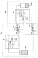
図1には、直流電力を給電する直流電源装置100と、直流電源装置100からの直流電力を受電する負荷10と、を含む直流電力供給システム1の構成例が示されている。直流電源装置100は、直流電力を給電する電源装置であり、例えば内部に蓄電池を備えて直流電力を負荷10へ給電するものであってもよく、太陽光、風力、地熱、バイオマスその他の自然エネルギーによって発電された電力を直流電力として負荷10へ給電するものであってもよい。
FIG. 1 shows a configuration example of a DC
負荷10は、直流電源装置100から直流電力の給電を受ける際には、プラグ11がプラグ受け20に挿入される。そして直流電源装置100からの直流電力の給電を停止する際には、プラグ11はプラグ受け20から抜去される。プラグ11がプラグ受け20から抜去される際に、アーク放電の抑制が考慮されていないと、上述したようにプラグ11やプラグ受け20の破損等に繋がる。
When the
そこで本実施形態では、直流電源装置100は、プラグ11がプラグ受け20から抜去される際のアーク放電を抑制するために、プラグ11がプラグ受け20から抜去される際に直流電源装置100から負荷10へ流れる電流を抑制するための電流制限回路を備える。
Therefore, in the present embodiment, the DC
直流電源装置100は、プラグ11がプラグ受け20に完全に挿入され、直流電源装置100から負荷10へ直流電力が給電されている際には、直流電源装置100に備えられる電流制限回路に電流が流れないような構成を有している。また、プラグ11がプラグ受け20から抜去される際には、電流制限回路を通じて直流電源装置100から負荷10へ電流を流しつつ、電流制限回路は、直流電源装置100から負荷10へ流れる電流を減少させる方向に機能する。
In the DC
本実施形態では、直流電源装置100に上述したような電流制限回路を備えることで、直流電力供給時の電力効率を低下させずに直流電力の切断時にアーク放電の発生を抑制することが出来る。また本実施形態に係る電流制限回路は、後述するように小規模の回路とすることが出来るので、回路規模を増大させること無く、直流電力の切断時にアーク放電の発生を抑制することが出来る。
In the present embodiment, by providing the DC
図2は、直流電源装置100の構成例を示す説明図である。図2に示したように、直流電源装置100は電流制限回路30を備える。また直流電源装置100が備えているプラグ受け20の正極側は2つの接触子20a、20bを、負極側は1つの接触子20cを、それぞれ備えている。
FIG. 2 is an explanatory diagram illustrating a configuration example of the DC
電流制限回路30は、プラグ11がプラグ受け20から抜去される際に、電流制限回路30を通じて直流電源装置100から負荷10へ電流を流しつつ、プラグ11がプラグ受け20から完全に抜去される際には、直流電源装置100から負荷10へ電流を流れる電流がアーク放電を生じさせない程度まで減少する方向に機能する回路である。そして電流制限回路30は、プラグ11がプラグ受け20に完全に挿入され、直流電源装置100から負荷10へ直流電力が給電されている際には電流が流れないような構成となっている。
When the
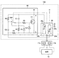
図3は、直流電源装置100の具体的な構成例を示す説明図である。図3に示したように、直流電源装置100は電流制限回路30を備える。また直流電源装置100が備えているプラグ受け20の正極側は2つの接触子20a、20bを、負極側は1つの接触子20cを、それぞれ備えている。
FIG. 3 is an explanatory diagram illustrating a specific configuration example of the DC
負荷10のプラグ11は、正極側端子11aと、負極側端子11bと、を備えている。図4は、プラグ11がプラグ受け20に挿入された状態を示す説明図である。プラグ11がプラグ受け20に挿入される際には、正極側端子11aは、まず接触子20bに接続され、接触子20bに接続された後に、図4に示したように接触子20aに接続される
The
図5は、プラグ11がプラグ受け20から抜去されていく状態を示す説明図である。プラグ11がプラグ受け20から抜去される際には、正極側端子11aが接触子20aに接続された状態から、抜去に伴って図5に示したように接触子20bに接続され、その後プラグ受け20から完全に抜去される。
FIG. 5 is an explanatory view showing a state in which the
電流制限回路30には、プラグ11がプラグ受け20に完全に挿入され、正極側端子11aが接触子20aと接触子20bとがショートされた状態では電流が流れず、正極側端子11aが接触子20bに接続された状態で電流が流れる。従って、プラグ11がプラグ受け20に完全に挿入された状態では電流制限回路30に電流が流れないので、直流電源装置100は、直流電力供給時の電力効率を低下させずに直流電力を負荷10へ給電することが出来る。
In the current limiting
電流制限回路30は、MOSFET T1と、コンデンサC1と、抵抗R1と、ダイオードD1と、を含んで構成される。電流制限回路30は電圧積分回路として機能する。
The current limiting
MOSFET T1は、本実施形態ではn型のMOSFET(Metal Oxide Semiconductor Field Effect Transistor) を用いており、プラグ11の正極側端子11aがプラグ受け20の接触子20bと接続している状態で、直流電源装置100から負荷10へ電流が流れる経路上に設けられる。コンデンサC1は、MOSFET T1のドレイン端子とゲート端子との間に設けられる。また抵抗R1は、MOSFET T1のゲート端子とソース端子との間に設けられる。そしてコンデンサC1と抵抗R1とは直列に接続されている。
In this embodiment, the MOSFET T1 uses an n-type MOSFET (Metal Oxide Field Effect Effect Transistor), and the DC power source is connected with the
電流制限回路30の機能について、図6、図7も併せて用いて説明する。図6は、プラグ11を備える負荷10が直流電源装置100のプラグ受け20に挿入された状態を横方向から模式的に示した説明図である。図6では正極側端子11aが接触子20a及び接触子20bの両方に接触している状態が示されている。また図6は、プラグ11からプラグ受け20から抜去される際の電流及び電圧の推移の例を示す説明図である。
The function of the current limiting
上述したようにプラグ11がプラグ受け20に完全に挿入され、正極側端子11aが接触子20aと接触子20bとの両方に接触して接触子20aと接触子20bとがショートされた状態では、電流制限回路30に電流が流れない。プラグ11がプラグ受け20から抜去され始めると、電流制限回路30の両端は正極側端子11aによりショートされているため、MOSFET T1もオフ状態にある。
As described above, in a state where the
その後、さらにプラグ11がプラグ受け20から抜去され続け、位置X1において正極側端子11aが接触子20aに接触しなくなり、接触子20bだけに接触するようになると、正極側端子11aと接触子20aとの接触点の一部に電流集中が発生し、その電流集中による電圧が接触子20aと接触子20bとの間に発生する。
Thereafter, when the
接触子20aと接触子20bとの間に発生した電圧はコンデンサC1を介してMOSFET T1のゲート電圧を誘起させて、MOSFET T1をオン状態にする。MOSFET T1がオン状態になると、接触子20aと接触子20bとの間の電圧を低下させる方向に電流が流れる。
The voltage generated between the
MOSFET T1がオン状態になり、接触子20aと接触子20bとの間の電圧を低下させる方向に電流が流れることにより、正極側端子11aと接触子20aとの電位差が低減される。正極側端子11aと接触子20aとの電位差が低減されることによって、正極側端子11aが接触子20aから離れてもアーク放電の発生に至ることはない。
The MOSFET T1 is turned on, and a current flows in a direction to decrease the voltage between the
MOSFET T1のドレイン端子とソース端子との間の電圧は、FETのゲート電圧による伝達関数に沿った電圧に収まる。正極側端子11aが接触子20aから離れてから、接触子20aと接触子20bとの間で発生した電圧によってコンデンサC1の充電が進むと、MOSFET T1のゲート電圧が低下し、MOSFET T1はオフ状態に移行することでMOSFET T1に電流が流れなくなる。MOSFET T1がオフ状態に移行した後に正極側端子11aが接触子20bから離れても、MOSFET T1に電流が流れていないので、アーク放電の発生に至ることはない。
The voltage between the drain terminal and the source terminal of the MOSFET T1 falls within the voltage along the transfer function due to the gate voltage of the FET. When the capacitor C1 is charged by the voltage generated between the
電流制限回路30の抵抗R1に並列に接続されたダイオードD1は、正極側端子11aが接触子20aと接触子20bとの両方に接触して接触子20aと接触子20bとがショートされた場合に、抵抗R1を介さずコンデンサC1に蓄積された電荷を短時間に放電するために設けられる。
The diode D1 connected in parallel to the resistor R1 of the current limiting
電流制限回路30において、ダイオードD1が抵抗R1と並列に設けられることで、例えば接触子20aと接触子20bとの接続がチャタリングなどの現象を起こしても、電流制限回路30の電圧積分機能が短時間で復帰できるようにしている。抵抗R1は、MOSFET T1のゲート端子に電圧を供給するが、電圧の供給時間はコンデンサC1の容量と抵抗R1の抵抗値との積の関係で決まる。
In the current limiting
図7は、プラグ11の挿入位置との関係による、電流制限回路30の両端電圧V1の電圧変化と、負荷10にかかる電圧V2の電圧変化を示している。また図7は、プラグ11の挿入位置との関係による、接触子20a側に流れる電流i1と接触子20b側に流れる電流i2の電流変化を示している。
FIG. 7 shows the voltage change of the both-ends voltage V1 of the current limiting
正極側端子11aが接触子20aから離れるX1の位置では、電流制限回路30の両端電圧V1は定電圧を維持するが、プラグ11の抜去が進むと、両端電圧V1は徐々に上昇するとともに、負荷10にかかる電圧V2が徐々に低下する。
At the position X1 where the
また、正極側端子11aが接触子20aから離れるX1の位置では、接触子20a側に流れる電流i1は0Aまで急激に低下するとともに、接触子20b側に流れる電流i2が0Aから急激に上昇する。電流i1は0Aまで急激に低下するとともに、電流i2が0Aから急激に上昇することで、電流制限回路30は、正極側端子11aと接触子20aとの間の電位差の発生を抑止している。
Further, at the position of X1 where the positive
そして正極側端子11aが接触子20bから離れるX2の位置では、負荷10にかかる電圧V2及び電流i2の低下が進んでおり、正極側端子11aと接触子20bとの間の電流集中が発生する条件が無くなっている。従って、正極側端子11aが接触子20bから離れても、アーク放電の発生に至ることはない。
Then, at the position X2 where the positive
なお、上述した例ではMOSFET T1としてn型のMOSFETを用いており、正極側に電圧積分機能を有する電流制限回路30を配置していたが、本開示は係る例に限定されるものではない。p型のMOSFETを用いて、負極に電圧積分機能を有する電流制限回路30を配置してもよい。
In the above-described example, an n-type MOSFET is used as the MOSFET T1, and the current limiting
また、上述した例では正極と負極とによる2線式での直流電力の給電の場合を示したが、正極、中性、負極による3線式での直流電力の給電の場合にも電圧積分機能を有する電流制限回路30を配置してもよい。3線式での直流電力の給電の場合は、正極と負極の両極に電流制限回路30を配置することで、プラグの抜去時のアーク放電の発生を抑制することが出来る。
Further, in the above-described example, the case of feeding DC power with a two-wire system using a positive electrode and a negative electrode has been shown. However, the voltage integration function is also used when feeding DC power with a three-wire system using a positive electrode, neutral and negative electrode. A current limiting
プラグ11の挿抜によって直流電源装置100からの直流給電の開始と停止が行われる例を示したが、本開示は係る例に限定されるものではない。図8は、直流電源装置100の変形例を示す説明図である。図8に示したのは、端子22a、22bを備えるスイッチ22の操作によって直流電源装置100からの直流給電の開始と停止が行われる例である。
Although an example in which the start and stop of the DC power supply from the DC
図8に示したスイッチ22は、直流電源装置100からの直流給電を開始する際には端子22a、22bが接触子21a、21bの両方に接触し、直流電源装置100からの直流給電を停止する際には、まず端子22bが接触子21bから離れ、端子22bが接触子21bから離れた後にバネ等の弾性力により端子22aが接触子21aから離れる構成となっている。
In the
図8に示したようにスイッチ22によって直流電源装置100からの直流給電の開始と停止が行われる場合であっても、電流制限回路30を配置することで、スイッチ22をオフする際のアーク放電の発生を抑制することが出来る。
Even when the DC power supply from the DC
図9は、直流電源装置100の変形例を示す説明図である。図9に示したのは、直流電源装置100にDCリレー31を備え、DCリレー31によって直流電源装置100からの直流給電の開始と停止が行われる例である。
FIG. 9 is an explanatory diagram illustrating a modification of the DC
図9のようにDCリレー31によって直流電源装置100からの直流給電の開始と停止を行う場合は、コンデンサC1に電荷がチャージされる瞬間にMOSFET T1がオンして過大な電流が負荷10へ流れる可能性がある。
When starting and stopping the DC power supply from the DC
そこで、コンデンサC1に電荷がチャージされる瞬間にMOSFET T1がオンして過大な電流が負荷10へ流れるのを回避するため、図9に示したように、コンデンサC1にチャージされる電荷による電流をDCリレー31のメーク接点で迂回させている。コンデンサC1にチャージされる電荷による電流をDCリレー31のメーク接点で迂回させていることで、過大な電流が負荷10へ流れるのを抑制することができる。
Therefore, in order to avoid the excessive current flowing to the
図10は、直流電源装置100にプラグ受け20が複数存在する場合の構成例を示す説明図である。図10に示したように、直流電源装置100にプラグ受け20が複数存在する場合であっても、1つの電流制限回路30によって、プラグ受け20からのプラグ11の抜去時のアーク放電の発生を抑制することが出来る。
FIG. 10 is an explanatory diagram illustrating a configuration example in the case where a plurality of
直流電力を給電する直流電源装置同士を接続する場合にも、それぞれの直流電源装置に電流制限回路を備えることで、それぞれの直流電源装置は、プラグ受け20からのプラグ11の抜去時のアーク放電の発生を抑制することが出来る。例えば、バッテリを備える直流電源装置同士を接続し、一方の直流電源装置から他方の直流電源装置のバッテリを充電するような場合に、それぞれの直流電源装置は、電流制限回路を備えることで、プラグ受け20からのプラグ11の抜去時のアーク放電の発生を抑制することが出来る。
Even when the DC power supply devices that supply DC power are connected to each other, each DC power supply device is provided with a current limiting circuit so that each DC power supply device can perform arc discharge when the
図11は、2つの直流電源装置100a、100bを接続する場合の構成例を示す説明図である。直流電源装置100aは接触子20a、20b、20cを備えるとともに、プラグの正極側端子11c、負極側端子11dを備えている。直流電源装置100bは接触子20d、20e、20fを備えるとともに、プラグの正極側端子11a、負極側端子11bを備えている。
FIG. 11 is an explanatory diagram illustrating a configuration example when two DC
例えば直流電源装置100bを直流電源装置100aに接続して直流電源装置100aから電力の供給を受ける場合、プラグの正極側端子11a、負極側端子11bが、直流電源装置100aに挿入される。そして直流電源装置100bは直流電源装置100aから電力の供給を停止する場合はプラグの正極側端子11a、負極側端子11bが直流電源装置100aから抜去されるが、抜去される際に電流制限回路30が機能し、正極側端子11aと接触子20a、20bとの間のアーク放電の発生が抑制される。
For example, when the DC
直流電源装置100aを直流電源装置100bに接続して直流電源装置100bから電力の供給を受ける場合も同様に、プラグの正極側端子11c、負極側端子11dが直流電源装置100bに挿入される。そして直流電源装置100aは、直流電源装置100bから電力の供給が停止される場合はプラグの正極側端子11c、負極側端子11dが直流電源装置100bから抜去される。プラグの正極側端子11c、負極側端子11dが直流電源装置100bから抜去される際に電流制限回路30が機能し、正極側端子11cと接触子20d、20eとの間のアーク放電の発生が抑制される。
Similarly, when the DC
なお、2つの直流電源装置100a、100bを接続する場合は、電流制限回路30のMOSFET T1のドレイン電極側にダイオードD2を設けることで、電流の逆流を防ぐことが望ましい。
When two DC
図11に示したようにバッテリを備える直流電源装置100a、100b同士を接続し、一方の直流電源装置から他方の直流電源装置のバッテリを充電するような場合に、直流電源装置100a、100bに電流制限回路30を備えることで、接触子からのプラグの端子の抜去時に、アーク放電が発生するのを抑制することが出来る。
As shown in FIG. 11, when the DC
ここまでは、プラグ受け20からのプラグ11の抜去時のアーク放電の発生を抑制するための構成例を示してきた。次に、プラグ受け20へのプラグ11の挿入時にスパーク(熱アーク)の発生を抑止するための構成例を説明する。
So far, the structural example for suppressing generation | occurrence | production of the arc discharge at the time of extraction of the
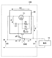
図12は、本開示の一実施形態に係る直流電源装置100の構成例を示す説明図である。図12に示した直流電源装置100は、プラグ受け20へのプラグ11の挿入時に発生するスパーク(熱アーク)の発生を抑止するための電流制限回路40を備えている。
FIG. 12 is an explanatory diagram illustrating a configuration example of the DC
電流制限回路40は、プラグ受け20へのプラグ11の挿入時に、直流電源装置100から負荷10へ電流が徐々に流れるように調整するための回路であり、MOSFET T1と、抵抗R2、R3と、コンデンサC2と、を含んで構成される。
The current limiting
プラグ11が図12のX3の位置まで挿入されると、抵抗R2、R3と、コンデンサC2とで電流積分回路が構成される。プラグ11が図12のX3の位置まで挿入された後に、プラグ11が図12のX2の位置まで挿入されると、抵抗R2、R3と、コンデンサC2とで構成された電流積分回路により、直流電源装置100から負荷10へ電流が徐々に流れる。
When the
そして、最終的にプラグ11が図12のX1の位置まで挿入されると、抵抗R2、R3と、コンデンサC2とで構成された電流積分回路による電流が低下して、MOSFET T1のゲート電圧が低下することにより、MOSFET T1がオフ状態になる。MOSFET T1がオフ状態になることで電流制限回路40への分流がなくなるので、図12に示した直流電源装置100は、直流電源装置100から負荷10へ効率良く電力を供給することが出来る。
When the
従って、図12に示した直流電源装置100は、プラグ受け20へプラグ11が挿入される際に、電流制限回路40によって直流電源装置100から負荷10へ電流を徐々に流すことで、プラグ受け20へプラグ11が挿入される際のスパーク(熱アーク)の発生を抑止することができる。
Accordingly, when the
ここで、図3等に示した電流制限回路30と、図12に示した電流制限回路40とを組み合わせることで、プラグ受け20へプラグ11が挿入される際のスパーク(熱アーク)の発生と、プラグ受け20からのプラグ11の抜去時のアーク放電の発生とを併せて抑制することが可能になる。図3等に示した電流制限回路30と、図12に示した電流制限回路40とを組み合わせた場合の例を説明する。
Here, by combining the current limiting
図13は、本開示の一実施形態に係る直流電源装置100の構成例を示す説明図である。図13に示した直流電源装置100は、プラグ受け20へプラグ11が挿入される際のスパーク(熱アーク)の発生と、プラグ受け20からのプラグ11の抜去時のアーク放電の発生とを抑止するための電流制限回路50を備えている。また図13に示したプラグ受け20は、負極側にも2つの接触子20c、20dが設けられている。
FIG. 13 is an explanatory diagram illustrating a configuration example of the DC
電流制限回路50は、図3等に示した電流制限回路30と、図12に示した電流制限回路40とを組み合わせた回路である。すなわち、電流制限回路50は、プラグ受け20へのプラグ11の挿入時に直流電源装置100から負荷10へ電流が徐々に流れるように機能するための回路であるとともに、プラグ受け20からのプラグ11の抜去時に直流電源装置100から負荷10へ電流が徐々に減少するように機能するための回路である。
The current limiting
電流制限回路50は、MOSFET T1と、抵抗R1、R2、R3と、コンデンサC1、C2と、ダイオードD1と、スイッチSW1と、を含んで構成される。スイッチSW1は、プラグ受け20へのプラグ11の挿入時にはMOSFET T1のゲート端子が抵抗R2に繋がり、プラグ受け20からのプラグ11の抜去時にはMOSFET T1のゲート端子が抵抗R1に繋がるような構造のスイッチである。
The current limiting
プラグ受け20へのプラグ11の挿入が開始されると、スイッチSW1は、プラグ受け20へのプラグ11の挿入に応じた摩擦力などに応じてMOSFET T1のゲート端子を抵抗R2に接続する方へスイッチング動作を行なう。逆に、プラグ受け20からのプラグ11の抜去が開始されると、プラグ受け20へのプラグ11の挿入に応じた摩擦力などに応じてMOSFET T1のゲート端子を抵抗R1に接続する方へスイッチング動作を行なう。
When the insertion of the
図13に示したスイッチSW1が、上述したようにスイッチング動作を行なうことで、電流制限回路50は、プラグ受け20へのプラグ11の挿入時に直流電源装置100から負荷10へ電流が徐々に流れるよう機能するとともに、プラグ受け20からのプラグ11の抜去時に直流電源装置100から負荷10へ電流が徐々に流れるように機能する。
When the switch SW1 shown in FIG. 13 performs the switching operation as described above, the current limiting
なお電流制限回路50は、図14に示したように、MOSFET T1を保護するための抵抗R3をゲート端子側に設けるとともに、同じくMOSFET T1を保護するためのツェナーダイオードDz1をMOSFET T1のゲート端子とソース端子との間に設けても良い。
As shown in FIG. 14, the current limiting
ここまでは、2つの端子と電極との接触で直流給電が行われる場合、すなわち、負荷10のプラグ11が2端子である場合の例を示したが、本開示は係る例に限定されるものではない。3つ以上の端子と電極との接触で直流給電が行われる場合にも、同様に電流制限回路によりアーク放電やスパーク(熱アーク)の発生を抑止できる。すなわち、負荷10のプラグや直流電源装置100の電極は3端子以上であっても良い。
Up to this point, an example has been shown where DC power is supplied by contact between two terminals and electrodes, that is, the case where the
図15は、本開示の一実施形態に係る直流電源装置100の構成例を示す説明図である。図15に示したのは、3つの端子によって直流給電を行なう直流電源装置100の構成例が示されている。図15に示した直流電源装置100は、プラグの端子111a、111b、111cがそれぞれ挿入される電極120a、120b、120cを備える。
FIG. 15 is an explanatory diagram illustrating a configuration example of the DC
プラグの端子111a、111b、111cが電極120a、120b、120cに挿入される際には、まず端子111b、111cが略同時に電極120b、120cに接触し、端子111b、111cが略同時に電極120b、120cに接触した後に端子111aが電極120aに接触する。
When the
そしてプラグの端子111a、111b、111cが電極120a、120b、120cから抜去される際には、まず端子111aが電極120aから離れ、端子111aが電極120aから離れた後に端子111b、111cが略同時に電極120b、120cから離れる。そして端子111aが電極120aから離れることで、電流制限回路30が、直流電源装置100から負荷10へ電流が徐々に減少するように機能し始める。
When the
図16は、本開示の一実施形態に係る直流電源装置100の構成例を示す説明図である。図16に示したのは、4つの端子によって直流給電を行なう直流電源装置100の構成例が示されている。図16に示した直流電源装置100は、プラグの端子111a、111b、111c、111dがそれぞれ挿入される電極120a、120b、120c、120dを備える。
FIG. 16 is an explanatory diagram illustrating a configuration example of the DC
プラグの端子111a、111b、111c、111dが電極120a、120b、120c、120dに挿入される際には、まず端子111b、111c、111dが略同時に電極120b、120c、120dに接触し、端子111b、111c、111dが略同時に電極120b、120c、120dに接触した後に端子111aが電極120aに接触する。端子111aが他の端子111b、111c、111dから送れて電極120aに接触することで、電流制限回路50が、直流電源装置100から負荷10へ電流が徐々に流れるよう機能し始める。
When the
そしてプラグの端子111a、111b、111c、111dが電極120a、120b、120c、120dから抜去される際には、まず端子111aが電極120aから離れ、端子111aが電極120aから離れた後に端子111b、111c、111dが略同時に電極120b、120c、120dから離れる。そして端子111aが電極120aから離れることで、電流制限回路50が、直流電源装置100から負荷10へ電流が徐々に減少するように機能し始める。
When the
上述したように、直流電源装置100は、3つ以上の端子と電極との接触で直流給電が行われる場合にも、2つの端子と電極との接触で直流給電が行われる場合と同様に、電流制限回路によってアーク放電やスパーク(熱アーク)の発生を抑止できる。
As described above, the direct-current
図17は、本開示の一実施形態に係る直流電源装置100の構成例を示す説明図である。図17に示したのは、直流電源装置100から負荷10を切り離す際に単極双投スイッチSW2を用いている直流電源装置100の構成例である。図17に示した例では、単極双投スイッチSW2のb接点を、電流制限回路30のコンデンサC1と抵抗R1との間の点と接続したことを特徴としている。直流電源装置100から負荷10を切り離す際に単極双投スイッチSW2を用いる場合であっても、電流制限回路30によってアーク放電やスパーク(熱アーク)の発生を抑止できる。
FIG. 17 is an explanatory diagram illustrating a configuration example of the DC
図18は、図17に示した直流電源装置100の構成例における電流及び電圧の推移例を示す説明図である。
FIG. 18 is an explanatory diagram showing an example of transition of current and voltage in the configuration example of the DC
直流電源装置100から負荷10へ直流給電が行われていない電源OFFの状態、すなわち、単極双投スイッチSW2がb接点の方に接続されている状態で、直流電源装置100に電圧が掛かる時、その電圧V2はコンデンサC1に掛かり、充電電流が流れる。コンデンサC1の容量が0.1μF程度の場合、微小な電流は負荷10に直接流れ、MOSFET T1はOFF状態を維持する。従って、MOSFET T1はOFF状態となっていることで、直流電源装置100から負荷10へ大きな電流は流れない。
When a voltage is applied to the DC
図18の時刻t1の時点で単極双投スイッチSW2が押されて、導通板がa接点に接続されると直流電源装置100の電圧V0は全て負荷10にかかり、電圧V0と負荷10の電圧V1とが同等の値になると、電流制限回路30はショート状態となる。電流制限回路30はショート状態となると、コンデンサC1に蓄積された電荷は、ダイオードD1を介して急速に放電される。
When the single-pole double-throw switch SW2 is pressed at time t1 in FIG. 18 and the conductive plate is connected to the contact a, all the voltages V0 of the DC
図18の時刻t2の時点で単極双投スイッチSW2が押されて、導通板とa接点との接続が解除されると、MOSFET T1のドレイン−ソース間電圧である電圧V2が上昇し始め、コンデンサC1に電流i3が流れる。コンデンサC1に電流i3が流れることで抵抗R1には電圧が発生し、MOSFET T1のゲート電圧VgがVg−onまで上昇するとMOSFET T1がONする。MOSFET T1がONすると、コンデンサC1の充電電圧が徐々に上昇していき、直流電源装置100から負荷10へ流れる電流i2が減少していく。
When the single-pole double-throw switch SW2 is pressed at time t2 in FIG. 18 and the connection between the conductive plate and the contact a is released, the voltage V2 that is the drain-source voltage of the MOSFET T1 starts to rise, A current i3 flows through the capacitor C1. When the current i3 flows through the capacitor C1, a voltage is generated in the resistor R1. When the gate voltage Vg of the MOSFET T1 rises to Vg-on, the MOSFET T1 is turned on. When the MOSFET T1 is turned on, the charging voltage of the capacitor C1 gradually increases, and the current i2 flowing from the DC
単極双投スイッチSW2の切り替え動作が終わると、図18の時刻t3の時点で単極双投スイッチSW2の導通板とb接点とが接続され、MOSFET T1のゲート電圧Vgが0Vとなり、直流電源装置100から負荷10へ流れる電流i2が遮断される。
When the switching operation of the single-pole double-throw switch SW2 is completed, the conduction plate of the single-pole double-throw switch SW2 and the b-contact are connected at time t3 in FIG. 18, the gate voltage Vg of the MOSFET T1 becomes 0 V, and the DC power supply The current i2 flowing from the
上述した一連の動作により、図17に示した直流電源装置100は、初期状態として負荷10に直流電源装置100の電圧V0が掛かった時に電流制限回路30が動作することを防いでいる。また、図17に示した直流電源装置100は、単極双投スイッチSW2のOFF動作時は導通板が接点aから十分離れ、接点bまで離れてもアーク放電が発生しない距離を確保できるとともに、電流制限回路30の動作を止めて、余計な電力消費を抑えるとともに、スイッチング素子であるMOSFET T1の発熱を抑えている。
By the series of operations described above, the DC
上述した一連の動作は、図9に示した、直流電源装置100にDCリレー31を備え、DCリレー31によって直流電源装置100からの直流給電の開始と停止が行われる構成例でも同様である。
The series of operations described above is the same in the configuration example shown in FIG. 9 in which the DC
図19は、本開示の一実施形態に係る直流電源装置100の構成例を示す説明図である。図19に示したのは、4つの端子によって直流給電を行なう直流電源装置100の構成例が示されている。図19に示した直流電源装置100は、プラグの端子111a、111b、111c、111dがそれぞれ挿入される電極120a、120b、120c、120dを備える。
FIG. 19 is an explanatory diagram illustrating a configuration example of the DC
プラグの端子111a、111b、111c、111dが電極120a、120b、120c、120dに挿入される際には、まず端子111b、111c、111dが略同時に電極120b、120c、120dに接触し、端子111b、111c、111dが略同時に電極120b、120c、120dに接触した後に端子111aが電極120aに接触する。
When the
そしてプラグの端子111a、111b、111c、111dが電極120a、120b、120c、120dから抜去される際には、まず端子111aが電極120aから離れ、端子111aが電極120aから離れた後に端子111b、111c、111dが略同時に電極120b、120c、120dから離れる。そして端子111aが電極120aから離れることで、電流制限回路30が、直流電源装置100から負荷10へ電流が徐々に減少するように機能し始める。
When the
図19に示した例では、プラグの端子111a、111cが同時に電極120a、120cに接触することはない。端子の先頭位置と末端位置とが、プラグの端子111a、111cとで異なっており、またに電極120a、120cの位置も、プラグの端子111a、111cが同時に電極120a、120cに接触しないような位置となっている。
In the example shown in FIG. 19, the
図19に示したようにプラグの端子111a、111b、111c、111d及び電極120a、120b、120c、120dが設けられることによっても、電流制限回路30によりアーク放電やスパーク(熱アーク)の発生を抑止できる。
As shown in FIG. 19, by providing the
図20は、本開示の一実施形態に係る直流電源装置100の構成例を示す説明図である。図20に示したのは、直流電源装置100から負荷10を切り離す際にスイッチSW3を用いている直流電源装置100の構成例である。図20には、プラグの端子11aとスイッチSW3との接触によりスイッチSW3の導通板が接点aと接点bとの間で切り替えられる構成が示されている。また、図20に示した例では、スイッチSW3のb接点を、電流制限回路30のコンデンサC1と抵抗R1との間の点と接続したことを特徴としている。
FIG. 20 is an explanatory diagram illustrating a configuration example of the DC
プラグが直流電源装置100に挿入される際には、接触子20aと端子11aとが、接触子20bと端子11bとが、それぞれ接触される。またプラグが直流電源装置100に挿入される際には、接触子20aと端子11aとの接触によって、スイッチSW3のb接点を介して、微小の電流がコンデンサC1へ流れ、コンデンサC1が充電される。
When the plug is inserted into the DC
その後、さらにプラグが直流電源装置100に挿入され、スイッチSW3が端子11aとの接触によって導通板が接点bから接点aへ切り替えられる。スイッチSW3の導通板が接点aへ切り替えられると、接点aを介して直流電源装置100からの直流電力が負荷10に供給される。またスイッチSW3の導通板が接点aへ切り替えられると、コンデンサC1に蓄えられていた電荷が、ダイオードD1を介して急速に放電される。
Thereafter, a plug is further inserted into the DC
プラグが直流電源装置100から抜去される際には、まずスイッチSW3が端子11bとの接触の解除によって導通板が接点aから接点bへ切り替えられる。スイッチSW3の導通板が接点aから切り離されると、電流制限回路30が動作し、直流電源装置100からの電流を電流制限回路30へ迂回することで、アーク放電の発生が抑制される。
When the plug is removed from the DC
そしてスイッチSW3の導通板が接点bと接続されると、MOSFET T1のゲート電圧が低下することでMOSFET T1がオフ状態となる。MOSFET T1がオフ状態となることで、直流電源装置100から負荷10へ流れる電流がゼロとなる。
When the conductive plate of the switch SW3 is connected to the contact b, the gate voltage of the MOSFET T1 is lowered, so that the MOSFET T1 is turned off. When the MOSFET T1 is turned off, the current flowing from the DC
図21は、本開示の一実施形態に係る直流電源装置100の構成例を示す説明図である。図21に示したのは、抵抗R1の替わりにサーミスタ150を用いた電流制限回路30を備える直流電源装置100の構成例である。
FIG. 21 is an explanatory diagram illustrating a configuration example of the DC
サーミスタ150は、抵抗値が温度に反比例するNTC(Negative Temperature Coefficient)サーミスタである。図21に示した電流制限回路30は、NTCサーミスタであるサーミスタ150に流れる電流によりサーミスタ150が自己発熱し、常温の時の抵抗値が急激に減少する効果を用いて、コンデンサC1の充電時間を短縮している。
The
図21に示した電流制限回路30は、コンデンサC1の充電時間を短縮できることで、MOSFET T1の動作時間を短縮させることができる。また、図21に示した電流制限回路30は、NTCサーミスタであるサーミスタ150の自己発熱による抵抗変化を利用し、コンデンサC1の充電時間を短くするとともに、直流電源の電源電圧の違いに関わらずMOSFET T1の電力消費による発熱を抑えながらアーク放電条件を抑圧することが出来る。
The current limiting
図22は、図21に示した電力制御装置100における、プラグ11の挿入位置との関係による、電流制限回路30の両端電圧V1の電圧変化と、負荷10にかかる電圧V2の電圧変化例を示す説明図である。また図22は、プラグ11の挿入位置との関係による、接触子20a側に流れる電流i1と接触子20b側に流れる電流i2の電流変化例も示している。なお図22には、図7で示した電圧変化のグラフにおける電圧V1、V2及び電流i1、i2が、それぞれ圧V1’、V2’及び電流i1’、i2’として破線で示されている。
FIG. 22 shows a voltage change example of the voltage V1 across the current limiting
図21に示した電流制限回路30は、NTCサーミスタであるサーミスタ150を用いることで、電圧V1、V2及び電流i1、i2が図22で示したグラフのように変化する。図21に示した電流制限回路30は、コンデンサC1の充電時間を短くすることで、電源電圧の違いに関わらずMOSFET T1の動作時間を短縮させ、MOSFET T1の電力消費による発熱を抑えながら、アーク放電の発生を抑制することが出来る。
The current limiting
図22には、プラグ11の挿入位置との関係によるMOSFET T1の消費電力Pの推移も示されている。電圧V1、V2及び電流i1、i2が図22で示したグラフのように変化することで、MOSFET T1の消費電力PもP’からPに変化する。すなわち、図21に示した電流制限回路30は、NTCサーミスタであるサーミスタ150を用いることで、MOSFET T1の消費電力量を抑えることが出来る。
FIG. 22 also shows the transition of the power consumption P of the MOSFET T1 depending on the relationship with the insertion position of the
なお、図21に示したサーミスタ150はNTCサーミスタを用いたが、NTCサーミスタに替えてCTR(Critical Temperature Resistor)サーミスタでもMOSFET T1の電力消費による発熱を抑えながら、アーク放電の発生を抑制する効果が期待できる。CTRサーミスタは、ある温度を超えると急激に抵抗が減少するサーミスタであり、抵抗値が温度に反比例するNTCサーミスタの替わりにCTRサーミスタを用いても、電流制限回路30はコンデンサC1の充電時間を短縮させることが出来る。
Although the
また、図21に示したNTCサーミスタであるサーミスタ150に並列に、抵抗またはPTC(Positive Temperature Coefficient)サーミスタを組み合わせることで、電流制限回路30の動作環境温度による積分時間の変動を抑えることもできる。PTCサーミスタは、CTRサーミスタと反対に、ある温度を超えると急激に抵抗が上昇するサーミスタである。NTCサーミスタとPTCサーミスタとを並列に組み合わせることで、電流制限回路30の動作環境温度が変動しても並列に組み合わされたサーミスタ全体としての抵抗値に大きな変動を生じさせないようにすることができる。
Further, by combining a
図21に示した電流制限回路30は、直流電源の電圧変化に対して積分時間が比例しないので、MOSFET T1の遮断時間を短縮することが出来る。また図21に示した直流制限回路30は、直流の遮断を行うにあたり、直流電源の電圧が2倍に変化してもMOSFET T1の消費電力がその電圧の増加に比例して大きくなることはなく、MOSFET T1の放熱を軽減することが出来る。
Since the integration time is not proportional to the voltage change of the DC power supply, the current limiting
図23は、電流制限回路30を備えた移動体200の機能構成例を示す説明図である。移動体200は、例えば、ガソリン車のようにガソリンを動力源とする移動体であってもよく、電気自動車、ハイブリッド車、電気オートバイ等の、充放電可能なバッテリを主な動力源とする移動体であってもよい。図23には、移動体200に、バッテリ210と、バッテリから供給される電力により駆動する駆動部220と、が備えられた場合の例が示されている。駆動部220には、例えばワイパー、パワーウィンドウ、ライト、カーナビゲーションシステム、エアーコンディショナのような車両に備えられる装備品や、モーター等の移動体200を駆動させる装置などが含まれうる。
FIG. 23 is an explanatory diagram illustrating a functional configuration example of the moving
そして図23に示した移動体200には、バッテリ210から駆動部220へ直流電力が供給される経路の途中に、電流制限回路30が設けられている。図23に示した移動体200は、バッテリ210から駆動部220へ直流電力が供給される経路上に、電流制限回路30が設けられることで、例えばバッテリ210を一時着脱させる際等にアーク放電の発生を抑えることが出来る。
In the moving
なお図23には、電流制限回路30が1つだけ備えられている移動体200の例を示したが、本開示は係る例に限定されるものではない。すなわち、電流制限回路30は直流電力が供給される経路の途中に複数設けられても良い。また電流制限回路30は、バッテリ210から駆動部220へ直流電力が供給される経路の途中だけでなく、他の場所、例えばバッテリ210を直流電力で充電する際の経路の途中に設けられても良い。移動体200は、バッテリ210を直流電力で充電する際の経路の途中に電流制限回路30を設けることで、安全にバッテリ210を直流電力で充電することができる。
FIG. 23 illustrates an example of the moving
<2.まとめ>
以上説明したように本開示の一実施形態によれば、直流電源装置100から負荷10へ直流給電が行われている際に直流電源装置100からプラグ11が抜去されると、直流電源装置100から負荷10へ流れる電流を徐々に低下させる方向に機能し、直流電源装置100からプラグ11が抜去された際のアーク放電の発生を抑制できる電流制限回路30を備えた直流電源装置100が提供される。
<2. Summary>
As described above, according to an embodiment of the present disclosure, when the
電流制限回路30は、直流電源装置100にプラグ11が完全に挿入された状態では電流が流れない。電流制限回路30は、直流電源装置100にプラグ11が完全に挿入された状態では電流が流れないことで、直流電源装置100から負荷10へ直流給電が行われている際に電力を消費することが無いので、電力の供給効率を低下させることが無い。
In the current limiting
そして電流制限回路30は、直流電源装置100からプラグ11が抜去される際にMOSFET T1のドレイン−ソース間に発生する電位差により生じる電流によって電荷をコンデンサC1で蓄積し、コンデンサC1での電荷の蓄積によってMOSFET T1のゲート電圧を上昇させて、MOSFET T1をオンする。
The current limiting
電流制限回路30は、コンデンサC1での電荷の蓄積によってMOSFET T1がオンされることによって直流電源装置100から負荷10への電流をMOSFET T1を通じて流すことで、それまでプラグ11の電極が接触していた接触子との間の電位差の発生を抑止して、直流電源装置100からプラグ11が抜去された際のアーク放電の発生を抑制することが出来る。
The current limiting
本開示の実施形態に係るプラグ11及びプラグ受け20は、それぞれUSB(Universal Serial Bus)のオス型コネクタ及びメス型コネクタに適用されても良い。USBのメス型コネクタからオス型コネクタへ直流の電力が供給される場合に、本開示の実施の形態に係る直流制限回路30がUSBポートを備える機器に設けられることで、USBのメス型コネクタからオス型コネクタが抜去された際のアーク放電の発生を抑えることが出来る。
The
以上、添付図面を参照しながら本開示の好適な実施形態について詳細に説明したが、本開示の技術的範囲はかかる例に限定されない。本開示の技術分野における通常の知識を有する者であれば、特許請求の範囲に記載された技術的思想の範疇内において、各種の変更例または修正例に想到し得ることは明らかであり、これらについても、当然に本開示の技術的範囲に属するものと了解される。 The preferred embodiments of the present disclosure have been described in detail above with reference to the accompanying drawings, but the technical scope of the present disclosure is not limited to such examples. It is obvious that a person having ordinary knowledge in the technical field of the present disclosure can come up with various changes or modifications within the scope of the technical idea described in the claims. Of course, it is understood that it belongs to the technical scope of the present disclosure.
また、本明細書に記載された効果は、あくまで説明的または例示的なものであって限定的ではない。つまり、本開示に係る技術は、上記の効果とともに、または上記の効果に代えて、本明細書の記載から当業者には明らかな他の効果を奏しうる。 Further, the effects described in the present specification are merely illustrative or exemplary and are not limited. That is, the technology according to the present disclosure can exhibit other effects that are apparent to those skilled in the art from the description of the present specification in addition to or instead of the above effects.
なお、以下のような構成も本開示の技術的範囲に属する。
(1)
直流電力の供給時に該直流電力を供給する電極に設けられる第1の接点に接触する前に、前記電極における該直流電力の供給時に電流が流れる受電側の端子が接触する位置に設けられる第2の接点と前記端子との接触が解除される前に、前記第2の接点を通じて前記端子へ流れる電流を減少させ、
前記端子が前記第1の接点に接触している場合は電流を流さず、前記端子が前記第2の接点に接触している場合にのみ前記第2の接点を通じて前記端子へ流れる電流を減少させる、電流制限回路。
(2)
前記第1の接点と前記第2の接点との間の電位差を徐々に上昇させることで前記直流電力を受電する機器の正極と負極との間の電位差を減少させ、前記第2の接点と前記端子との間に流れる電流を減少させる、前記(1)に記載の電流制限回路。
(3)
前記端子が前記第1の接点に接続されなくなった時点でオン状態になり、前記端子が前記第2の接点にのみ接続された状態で前記第2の接点を通じて前記端子へ流れる電流を減少させるスイッチング素子を備える、前記(2)に記載の電流制限回路。
(4)
前記端子が前記第1の接点に接続されなくなった時点で充電が開始され、前記端子が前記第2の接点にのみ接続された状態で前記スイッチング素子のゲート電圧を上昇させる容量素子を備える、前記(3)に記載の電流制限回路。
(5)
前記スイッチング素子のゲート端子に電圧を印加する時間を、前記容量素子と共に設定する抵抗素子を備える、前記(4)に記載の電流制限回路。
(6)
前記抵抗素子は、抵抗値が温度上昇に伴い低下する素子である、前記(5)に記載の電流制限回路。
(7)
前記端子が前記第1の接点と接触する前に前記第2の接点と接触する際に、前記第2の接点を通じて前記端子へ流れる電流を徐々に増加させる、前記(1)〜(6)のいずれかに記載の電流制限回路。
(8)
前記端子が前記第1の接点と接触する前に前記第2の接点と接触する場合と、前記端子が前記第1の接点と接触してから前記第2の接点と接触する場合との機能を切り替えるスイッチを備える、前記(7)に記載の電流制限回路。
(9)
直流電力を供給する正極側電極及び負極側電極を少なくとも備え、
前記正極側電極または負極側電極の少なくともいずれかは、
第1の接点と、
前記直流電力の供給時に直流電流が流れる受電側の端子が前記第1の接点に接触する前に接触する位置に設けられる第2の接点と、
前記端子と前記第2の接点との接触が解除される前に前記第2の接点を通じて前記端子へ流れる電流を減少させる電流制限回路と、
を備え、
前記電流制限回路は、前記端子が前記第1の接点に接触している場合は電流を流さず、前記端子が前記第2の接点に接触している場合にのみ前記第2の接点を通じて前記端子へ流れる電流を減少させる、直流電力供給コネクタ。
(10)
前記電流制限回路は、前記第1の接点と前記第2の接点との間の電位差を徐々に上昇させることで前記直流電力を受電する機器の正極と負極との間の電位差を減少させ、前記第2の接点と前記端子との間に流れる電流を減少させる、前記(9)に記載の直流電力供給コネクタ。
(11)
前記電流制限回路は、前記端子が前記第1の接点に接続されなくなった時点でオン状態になり、前記端子が前記第2の接点にのみ接続された状態で前記第2の接点を通じて前記端子へ流れる電流を減少させるスイッチング素子を備える、前記(10)に記載の直流電力供給コネクタ。
(12)
前記電流制限回路は、前記端子が前記第1の接点に接続されなくなった時点で充電が開始され、前記端子が前記第2の接点にのみ接続された状態で前記スイッチング素子のゲート電圧を上昇させる容量素子を備える、前記(11)に記載の直流電力供給コネクタ。
(13)
前記電流制限回路は、前記スイッチング素子のゲート端子に電圧を印加する時間を、前記容量素子と共に設定する抵抗素子を備える、前記(12)に記載の直流電力供給コネクタ。
(14)
前記抵抗素子は、抵抗値が温度上昇に伴い低下する素子である、前記(13)に記載の電流制限コネクタ。
(15)
前記電流制限回路は、前記端子が前記第1の接点と接触する前に前記第2の接点と接触する際に、前記第2の接点を通じて前記端子へ流れる電流を徐々に増加させる、前記(9)〜(14)のいずれかに記載の直流電力供給コネクタ。
(16)
前記電流制限回路は、前記端子が前記第1の接点と接触する前に前記第2の接点と接触する場合と、前記端子が前記第1の接点と接触してから前記第2の接点と接触する場合との機能を切り替えるスイッチを備える、前記(15)に記載の電流制限コネクタ。
(17)
直流電力を供給する直流電源と、
前記直流電源からの直流電力を供給する正極側電極及び負極側電極と、
を少なくとも備え、
前記正極側電極または負極側電極の少なくともいずれかは、
第1の接点と、
前記直流電力の供給時に直流電流が流れる受電側の端子が前記第1の接点に接触する前に接触する位置に設けられる第2の接点と、
前記端子と前記第2の接点との接触が解除される前に前記第2の接点を通じて前記端子へ流れる電流を減少させる電流制限回路と、
を備え、
前記電流制限回路は、前記端子が前記第1の接点に接触している場合は電流を流さず、前記端子が前記第2の接点に接触している場合にのみ前記第2の接点を通じて前記端子へ流れる電流を減少させる、直流電源装置。
(18)
前記電流制限回路は、前記第1の接点と前記第2の接点との間の電位差を徐々に上昇させることで前記直流電力を受電する機器の正極と負極との間の電位差を減少させ、前記第2の接点と前記端子との間に流れる電流を減少させる、前記(17)に記載の直流電源装置。
(19)
前記端子が前記第1の接点に接続されなくなった時点でオン状態になり、前記端子が前記第2の接点にのみ接続された状態で前記第2の接点を通じて前記端子へ流れる電流を減少させるスイッチング素子を備える、前記(18)に記載の直流電源装置。
(20)
前記電流制限回路は、前記端子が前記第1の接点に接続されなくなった時点で充電が開始され、前記端子が前記第2の接点にのみ接続された状態で前記スイッチング素子のゲート電圧を上昇させる容量素子を備える、前記(19)に記載の直流電源装置。
(21)
前記電流制限回路は、前記スイッチング素子のゲート端子に電圧を印加する時間を、前記容量素子と共に設定する抵抗素子を備える、前記(20)に記載の直流電源装置。
(22)
前記抵抗素子は、抵抗値が温度上昇に伴い低下する素子である、前記(21)に記載の直流電源装置。
(23)
前記電流制限回路は、前記端子が前記第1の接点と接触する前に前記第2の接点と接触する際に、前記第2の接点を通じて前記端子へ流れる電流を徐々に増加させる、前記(17)〜(22)のいずれかに記載の直流電源装置。
(24)
前記電流制限回路は、前記端子が前記第1の接点と接触する前に前記第2の接点と接触する場合と、前記端子が前記第1の接点と接触してから前記第2の接点と接触する場合との機能を切り替えるスイッチを備える、前記(23)に記載の直流電源装置。
(25)
直流電力の供給を受ける端子がドレイン側の接点と接続しなくなった時点でオン状態になり、前記端子がソース側の接点にのみ接続された状態で前記ソース側の接点を通じて前記端子へ流れる電流を減少させるスイッチング素子と、
端子が前記ドレイン側の接点に接続されなくなった時点で充電が開始され、前記端子が前記ソース側の接点にのみ接続された状態で前記スイッチング素子のゲート電圧を上昇させる容量素子と、
前記スイッチング素子のゲート端子に電圧を印加する時間を、前記容量素子と共に設定する抵抗素子と、
を備える、電流制限回路。
(26)
前記ドレイン側の接点と前記ソース側の接点との間の電位差を徐々に上昇させることで前記直流電力を受電する機器の正極と負極との間の電位差を減少させ、前記ソース側の接点と前記端子との間に流れる電流を減少させる、前記(25)に記載の電流制限回路。
(27)
前記抵抗素子は、抵抗値が温度上昇に伴い低下する素子である、前記(25)または(26)に記載の電流制限回路。
(28)
前記端子が前記ドレイン側の接点と接触する前に前記ソース側の接点と接触する際に、前記ソース側の接点を通じて前記端子へ流れる電流を徐々に増加させる、前記(25)〜(27)のいずれかに記載の電流制限回路。
(29)
前記端子が前記ドレイン側の接点と接触する前に前記ソース側の接点と接触する場合と、前記端子が前記ドレイン側の接点と接触してから前記ソース側の接点と接触する場合との機能を切り替えるスイッチを備える、前記(28)に記載の電流制限回路。
(30)
前記(1)〜(8)のいずれかに記載の電流制限回路を備える、移動体。
(31)
直流電力を供給するバッテリと、
前記バッテリから供給される直流電力による駆動する駆動部と、
前記バッテリと前記駆動部との間に設けられる、少なくとも1つの、請求項1に記載の電流制限回路と、
を備える、電力供給システム。
(32)
前記電力供給システムは、移動体に備えられる、前記(31)に記載の電力供給システム。
(33)
前記電流制限回路は、前記第1の接点と前記第2の接点との間の電位差を徐々に上昇させることで前記直流電力を受電する機器の正極と負極との間の電位差を減少させ、前記第2の接点と前記端子との間に流れる電流を減少させる、前記(31)または(32)に記載の電力供給システム。
(34)
前記端子が前記第1の接点に接続されなくなった時点でオン状態になり、前記端子が前記第2の接点にのみ接続された状態で前記第2の接点を通じて前記端子へ流れる電流を減少させるスイッチング素子を備える、前記(33)に記載の電力供給システム。
(35)
前記電流制限回路は、前記端子が前記第1の接点に接続されなくなった時点で充電が開始され、前記端子が前記第2の接点にのみ接続された状態で前記スイッチング素子のゲート電圧を上昇させる容量素子を備える、前記(34)に記載の電力供給システム。
(36)
前記電流制限回路は、前記スイッチング素子のゲート端子に電圧を印加する時間を、前記容量素子と共に設定する抵抗素子を備える、前記(35)に記載の電力供給システム。
(37)
前記抵抗素子は、抵抗値が温度上昇に伴い低下する素子である、前記(36)に記載の電力供給システム。
(38)
前記電流制限回路は、前記端子が前記第1の接点と接触する前に前記第2の接点と接触する際に、前記第2の接点を通じて前記端子へ流れる電流を徐々に増加させる、前記(31)〜(37)のいずれかに記載の電力供給システム。
(39)
前記電流制限回路は、前記端子が前記第1の接点と接触する前に前記第2の接点と接触する場合と、前記端子が前記第1の接点と接触してから前記第2の接点と接触する場合との機能を切り替えるスイッチを備える、前記(38)に記載の電力供給システム。
The following configurations also belong to the technical scope of the present disclosure.
(1)
A second terminal provided at a position where the terminal on the power receiving side through which a current flows when the DC power is supplied contacts the electrode before contacting the first contact provided on the electrode that supplies the DC power when the DC power is supplied. Before the contact between the contact and the terminal is released, the current flowing to the terminal through the second contact is reduced,
When the terminal is in contact with the first contact, no current is passed, and only when the terminal is in contact with the second contact, the current flowing to the terminal through the second contact is reduced. Current limiting circuit.
(2)
By gradually increasing the potential difference between the first contact and the second contact, the potential difference between the positive electrode and the negative electrode of the device receiving the DC power is reduced, and the second contact and the The current limiting circuit according to (1), wherein the current flowing between the terminals is reduced.
(3)
Switching that turns on when the terminal is no longer connected to the first contact, and reduces the current flowing to the terminal through the second contact with the terminal connected only to the second contact The current limiting circuit according to (2), including an element.
(4)
Charging is started when the terminal is no longer connected to the first contact, and includes a capacitive element that raises the gate voltage of the switching element in a state where the terminal is connected only to the second contact, The current limiting circuit according to (3).
(5)
The current limiting circuit according to (4), further including a resistance element that sets a time for applying a voltage to the gate terminal of the switching element together with the capacitance element.
(6)
The current limiting circuit according to (5), wherein the resistance element is an element whose resistance value decreases with increasing temperature.
(7)
(1) to (6), wherein when the terminal contacts the second contact before contacting the first contact, the current flowing to the terminal through the second contact is gradually increased. The current limiting circuit according to any one of the above.
(8)
Functions of the case where the terminal contacts the second contact before contacting the first contact and the case where the terminal contacts the second contact after the terminal contacts the first contact. The current limiting circuit according to (7), further including a switch for switching.
(9)
Comprising at least a positive electrode and a negative electrode for supplying DC power;
At least one of the positive electrode or the negative electrode is:
A first contact;
A second contact provided at a position where a terminal on the power receiving side through which a direct current flows when the DC power is supplied contacts the first contact;
A current limiting circuit for reducing a current flowing to the terminal through the second contact before the contact between the terminal and the second contact is released;
With
The current limiting circuit does not pass current when the terminal is in contact with the first contact, and passes through the second contact only when the terminal is in contact with the second contact. DC power supply connector that reduces the current flowing to
(10)
The current limiting circuit reduces a potential difference between a positive electrode and a negative electrode of a device that receives the DC power by gradually increasing a potential difference between the first contact and the second contact, The DC power supply connector according to (9), wherein a current flowing between a second contact and the terminal is reduced.
(11)
The current limiting circuit is turned on when the terminal is no longer connected to the first contact, and is connected to the terminal through the second contact with the terminal connected only to the second contact. The DC power supply connector according to (10), further including a switching element that reduces a flowing current.
(12)
The current limiting circuit starts charging when the terminal is not connected to the first contact, and increases the gate voltage of the switching element in a state where the terminal is connected only to the second contact. The direct-current power supply connector according to (11), including a capacitive element.
(13)
The DC power supply connector according to (12), wherein the current limiting circuit includes a resistance element that sets a time for applying a voltage to the gate terminal of the switching element together with the capacitance element.
(14)
The current limiting connector according to (13), wherein the resistance element is an element whose resistance value decreases with increasing temperature.
(15)
The current limiting circuit gradually increases a current that flows to the terminal through the second contact when the terminal contacts the second contact before contacting the first contact. )-(14) The direct-current power supply connector in any one of.
(16)
The current limiting circuit includes a case where the terminal contacts the second contact before the terminal contacts the first contact, and a case where the terminal contacts the first contact after the terminal contacts the first contact. The current limiting connector according to (15), further including a switch that switches a function with a case where the function is performed.
(17)
A DC power supply for supplying DC power;
A positive electrode and a negative electrode for supplying DC power from the DC power source;
Comprising at least
At least one of the positive electrode or the negative electrode is:
A first contact;
A second contact provided at a position where a terminal on the power receiving side through which a direct current flows when the DC power is supplied contacts the first contact;
A current limiting circuit for reducing a current flowing to the terminal through the second contact before the contact between the terminal and the second contact is released;
With
The current limiting circuit does not pass current when the terminal is in contact with the first contact, and passes through the second contact only when the terminal is in contact with the second contact. DC power supply that reduces the current flowing to
(18)
The current limiting circuit reduces a potential difference between a positive electrode and a negative electrode of a device that receives the DC power by gradually increasing a potential difference between the first contact and the second contact, The DC power supply device according to (17), wherein a current flowing between a second contact and the terminal is reduced.
(19)
Switching that turns on when the terminal is no longer connected to the first contact, and reduces the current flowing to the terminal through the second contact with the terminal connected only to the second contact The direct-current power supply device according to (18), including an element.
(20)
The current limiting circuit starts charging when the terminal is not connected to the first contact, and increases the gate voltage of the switching element in a state where the terminal is connected only to the second contact. The direct current power supply device according to (19), including a capacitive element.
(21)
The DC power supply device according to (20), wherein the current limiting circuit includes a resistance element that sets a time for applying a voltage to the gate terminal of the switching element together with the capacitance element.
(22)
The direct-current power supply device according to (21), wherein the resistance element is an element whose resistance value decreases with increasing temperature.
(23)
The current limiting circuit gradually increases a current flowing to the terminal through the second contact when the terminal contacts the second contact before contacting the first contact. The DC power supply device according to any one of (22) to (22).
(24)
The current limiting circuit includes a case where the terminal contacts the second contact before the terminal contacts the first contact, and a case where the terminal contacts the first contact after the terminal contacts the first contact. The direct-current power supply device according to (23), further including a switch that switches a function with a case where the function is performed.
(25)
When a terminal receiving DC power is not connected to a drain-side contact, the terminal is turned on, and the current flowing to the terminal through the source-side contact with the terminal connected only to the source-side contact A switching element to reduce,
Charging starts when the terminal is no longer connected to the drain-side contact, and the capacitive element increases the gate voltage of the switching element in a state where the terminal is connected only to the source-side contact;
A resistive element for setting a time for applying a voltage to the gate terminal of the switching element together with the capacitive element;
A current limiting circuit.
(26)
By gradually increasing the potential difference between the drain-side contact and the source-side contact, the potential difference between the positive electrode and the negative electrode of the device receiving the DC power is reduced, and the source-side contact and the The current limiting circuit according to (25), wherein the current flowing between the terminals is reduced.
(27)
The current limiting circuit according to (25) or (26), wherein the resistance element is an element whose resistance value decreases with increasing temperature.
(28)
(25) to (27), wherein the current flowing to the terminal through the source-side contact is gradually increased when the terminal contacts the source-side contact before contacting the drain-side contact. The current limiting circuit according to any one of the above.
(29)
The function of the case where the terminal contacts the source side contact before contacting the drain side contact and the case where the terminal contacts the drain side contact after the terminal contacts the drain side contact. The current limiting circuit according to (28), further including a switch for switching.
(30)
A moving body comprising the current limiting circuit according to any one of (1) to (8).
(31)
A battery for supplying DC power;
A drive unit driven by DC power supplied from the battery;
At least one current limiting circuit according to
A power supply system comprising:
(32)
The power supply system according to (31), wherein the power supply system is provided in a moving body.
(33)
The current limiting circuit reduces a potential difference between a positive electrode and a negative electrode of a device that receives the DC power by gradually increasing a potential difference between the first contact and the second contact, The power supply system according to (31) or (32), wherein a current flowing between a second contact and the terminal is reduced.
(34)
Switching that turns on when the terminal is no longer connected to the first contact, and reduces the current flowing to the terminal through the second contact with the terminal connected only to the second contact The power supply system according to (33), including an element.
(35)
The current limiting circuit starts charging when the terminal is not connected to the first contact, and increases the gate voltage of the switching element in a state where the terminal is connected only to the second contact. The power supply system according to (34), including a capacitive element.
(36)
The power supply system according to (35), wherein the current limiting circuit includes a resistance element that sets a time for applying a voltage to the gate terminal of the switching element together with the capacitance element.
(37)
The power supply system according to (36), wherein the resistance element is an element whose resistance value decreases as the temperature increases.
(38)
The current limiting circuit gradually increases a current that flows to the terminal through the second contact when the terminal contacts the second contact before contacting the first contact. The power supply system according to any one of (37) to (37).
(39)
The current limiting circuit includes a case where the terminal contacts the second contact before the terminal contacts the first contact, and a case where the terminal contacts the first contact after the terminal contacts the first contact. The power supply system according to (38), further including a switch that switches a function with a case where the function is performed.
1 :直流電力供給システム
10 :負荷
11 :プラグ
11a :正極側端子
11b :負極側端子
11c :正極側端子
11d :負極側端子
20 :プラグ受け
20a、20b、20c、20d、20e、20f、21a、21b :接触子
22 :スイッチ
22a、22b :端子
30、40、50 :電流制限回路
31 :DCリレー
100、100a、100b :直流電源装置
111a、111b、111c、111d :端子
120a、120b、120c、120d :電極
200 :移動体
210 :バッテリ
220 :駆動部
1: DC power supply system 10: Load 11:
Claims (35)
前記端子が前記第1の接点に接触している場合は前記第2の接点への電流を遮断し、前記端子が前記第2の接点に接触している場合にのみ前記第2の接点を通じて前記端子へ流れる電流を減少させ、前記端子が前記第1の接点と接触する前に前記第2の接点と接触する際に、前記第2の接点を通じて前記端子へ流れる電流を徐々に増加させる、電流制限回路。 A second terminal provided at a position where the terminal on the power receiving side through which a current flows when the DC power is supplied contacts the electrode before contacting the first contact provided on the electrode that supplies the DC power when the DC power is supplied. Before the contact between the contact and the terminal is released, the current flowing to the terminal through the second contact is reduced,
When the terminal is in contact with the first contact, the current to the second contact is cut off, and only when the terminal is in contact with the second contact, through the second contact reducing the current flowing to the terminal, when said terminal is in contact with the second contact prior to contact with said first contact, Ru gradually increasing the current flowing into the terminal through the second contact, Current limit circuit.
前記正極側電極または負極側電極の少なくともいずれかは、
第1の接点と、
前記直流電力の供給時に直流電流が流れる受電側の端子が前記第1の接点に接触する前に接触する位置に設けられる第2の接点と、
前記端子と前記第2の接点との接触が解除される前に前記第2の接点を通じて前記端子へ流れる電流を減少させる電流制限回路と、
を備え、
前記電流制限回路は、前記端子が前記第1の接点に接触している場合は前記第2の接点への電流を遮断し、前記端子が前記第2の接点に接触している場合にのみ前記第2の接点を通じて前記端子へ流れる電流を減少させ、前記端子が前記第1の接点と接触する前に前記第2の接点と接触する際に、前記第2の接点を通じて前記端子へ流れる電流を徐々に増加させる、直流電力供給コネクタ。 Comprising at least a positive electrode and a negative electrode for supplying DC power;
At least one of the positive electrode or the negative electrode is:
A first contact;
A second contact provided at a position where a terminal on the power receiving side through which a direct current flows when the DC power is supplied contacts the first contact;
A current limiting circuit for reducing a current flowing to the terminal through the second contact before the contact between the terminal and the second contact is released;
With
The current limiting circuit cuts off a current to the second contact when the terminal is in contact with the first contact, and only when the terminal is in contact with the second contact. The current flowing to the terminal through the second contact is reduced, and the current flowing to the terminal through the second contact is reduced when the terminal contacts the second contact before contacting the first contact. gradually Ru increases, the DC power supply connector.
前記直流電源からの直流電力を供給する正極側電極及び負極側電極と、
を少なくとも備え、
前記正極側電極または負極側電極の少なくともいずれかは、
第1の接点と、
前記直流電力の供給時に直流電流が流れる受電側の端子が前記第1の接点に接触する前に接触する位置に設けられる第2の接点と、
前記端子と前記第2の接点との接触が解除される前に前記第2の接点を通じて前記端子へ流れる電流を減少させる電流制限回路と、
を備え、
前記電流制限回路は、前記端子が前記第1の接点に接触している場合は前記第2の接点への電流を遮断し、前記端子が前記第2の接点に接触している場合にのみ前記第2の接点を通じて前記端子へ流れる電流を減少させ、前記端子が前記第1の接点と接触する前に前記第2の接点と接触する際に、前記第2の接点を通じて前記端子へ流れる電流を徐々に増加させる、直流電源装置。 A DC power supply for supplying DC power;
A positive electrode and a negative electrode for supplying DC power from the DC power source;
Comprising at least
At least one of the positive electrode or the negative electrode is:
A first contact;
A second contact provided at a position where a terminal on the power receiving side through which a direct current flows when the DC power is supplied contacts the first contact;
A current limiting circuit for reducing a current flowing to the terminal through the second contact before the contact between the terminal and the second contact is released;
With
The current limiting circuit cuts off a current to the second contact when the terminal is in contact with the first contact, and only when the terminal is in contact with the second contact. The current flowing to the terminal through the second contact is reduced, and the current flowing to the terminal through the second contact is reduced when the terminal contacts the second contact before contacting the first contact. gradually Ru increases, the DC power supply.
端子が前記ドレイン側の接点に接続されなくなった時点で充電が開始され、前記端子が前記ソース側の接点にのみ接続された状態で前記スイッチング素子のゲート電圧を上昇させる容量素子と、
前記スイッチング素子のゲート端子に電圧を印加する時間を、前記容量素子と共に設定する抵抗素子と、
を備える、電流制限回路。 When a terminal receiving DC power is not connected to a drain-side contact, the terminal is turned on, and the current flowing to the terminal through the source-side contact with the terminal connected only to the source-side contact A switching element to reduce,
Charging starts when the terminal is no longer connected to the drain-side contact, and the capacitive element increases the gate voltage of the switching element in a state where the terminal is connected only to the source-side contact;
A resistive element for setting a time for applying a voltage to the gate terminal of the switching element together with the capacitive element;
A current limiting circuit.
前記バッテリから供給される直流電力による駆動する駆動部と、
前記バッテリと前記駆動部との間に設けられる、少なくとも1つの、請求項1に記載の電流制限回路と、
を備える、電力供給システム。 A battery for supplying DC power;
A drive unit driven by DC power supplied from the battery;
At least one current limiting circuit according to claim 1, provided between the battery and the drive unit;
A power supply system comprising:
Priority Applications (10)
| Application Number | Priority Date | Filing Date | Title |
|---|---|---|---|
| JP2015094751A JP5862818B1 (en) | 2015-01-30 | 2015-05-07 | Current limiting circuit, DC power supply connector, and DC power supply device |
| EP15880035.9A EP3252882A4 (en) | 2015-01-30 | 2015-05-26 | Current limiting circuit, dc power supply connector, and dc power supply device |
| US15/545,016 US10910828B2 (en) | 2015-01-30 | 2015-05-26 | Current limiting circuit, DC power supply connector, and DC power source device |
| BR112017015677-6A BR112017015677A2 (en) | 2015-01-30 | 2015-05-26 | A current restriction circuit, a direct-current electric power supply connector, and a DC power unit |
| CN201580073145.7A CN107112747B (en) | 2015-01-30 | 2015-05-26 | current limiting circuit, DC power supply connector, and DC power supply device |
| MYPI2017702683A MY198029A (en) | 2015-01-30 | 2015-05-26 | Current limiting circuit, dc power supply connector, and dc power source device |
| KR1020177019798A KR20170113549A (en) | 2015-01-30 | 2015-05-26 | Current limiting circuit, dc power supply connector, and dc power supply device |
| RU2017125968A RU2017125968A (en) | 2015-01-30 | 2015-05-26 | DC LIMIT DIAGRAM, DC CONNECTOR POWER SUPPLY CONNECTOR, AND DC POWER SUPPLY POWER SUPPLY |
| PCT/JP2015/065071 WO2016121140A1 (en) | 2015-01-30 | 2015-05-26 | Current limiting circuit, dc power supply connector, and dc power supply device |
| TW104144477A TWI683485B (en) | 2015-01-30 | 2015-12-30 | Current limiting circuit, DC power supply connector and DC power supply device |
Applications Claiming Priority (5)
| Application Number | Priority Date | Filing Date | Title |
|---|---|---|---|
| JP2015016273 | 2015-01-30 | ||
| JP2015016273 | 2015-01-30 | ||
| JP2015056005 | 2015-03-19 | ||
| JP2015056005 | 2015-03-19 | ||
| JP2015094751A JP5862818B1 (en) | 2015-01-30 | 2015-05-07 | Current limiting circuit, DC power supply connector, and DC power supply device |
Related Child Applications (1)
| Application Number | Title | Priority Date | Filing Date |
|---|---|---|---|
| JP2015199021A Division JP6641862B2 (en) | 2015-01-30 | 2015-10-07 | Current limiting circuit, DC power supply connector and DC power supply |
Publications (2)
| Publication Number | Publication Date |
|---|---|
| JP5862818B1 true JP5862818B1 (en) | 2016-02-16 |
| JP2016174517A JP2016174517A (en) | 2016-09-29 |
Family
ID=55305522
Family Applications (2)
| Application Number | Title | Priority Date | Filing Date |
|---|---|---|---|
| JP2015094751A Active JP5862818B1 (en) | 2015-01-30 | 2015-05-07 | Current limiting circuit, DC power supply connector, and DC power supply device |
| JP2015199021A Active JP6641862B2 (en) | 2015-01-30 | 2015-10-07 | Current limiting circuit, DC power supply connector and DC power supply |
Family Applications After (1)
| Application Number | Title | Priority Date | Filing Date |
|---|---|---|---|
| JP2015199021A Active JP6641862B2 (en) | 2015-01-30 | 2015-10-07 | Current limiting circuit, DC power supply connector and DC power supply |
Country Status (10)
| Country | Link |
|---|---|
| US (1) | US10910828B2 (en) |
| EP (1) | EP3252882A4 (en) |
| JP (2) | JP5862818B1 (en) |
| KR (1) | KR20170113549A (en) |
| CN (1) | CN107112747B (en) |
| BR (1) | BR112017015677A2 (en) |
| MY (1) | MY198029A (en) |
| RU (1) | RU2017125968A (en) |
| TW (1) | TWI683485B (en) |
| WO (1) | WO2016121140A1 (en) |
Cited By (3)
| Publication number | Priority date | Publication date | Assignee | Title |
|---|---|---|---|---|
| JP2016173984A (en) * | 2015-01-30 | 2016-09-29 | ソニー株式会社 | Current limiting circuit, dc power supply connector, and dc power supply device |
| JP2017157446A (en) * | 2016-03-02 | 2017-09-07 | 河村電器産業株式会社 | Dc receptacle device |
| JP2019187225A (en) * | 2018-04-06 | 2019-10-24 | ヤザキ・ノース・アメリカ,インコーポレイテッド | Method and apparatus for dc arc detection/suppression |
Families Citing this family (11)
| Publication number | Priority date | Publication date | Assignee | Title |
|---|---|---|---|---|
| FR3030105B1 (en) * | 2014-12-11 | 2017-05-26 | Inst Supergrid | HIGH VOLTAGE CONTINUOUS CURRENT CUTTING DEVICE |
| US10454224B2 (en) * | 2015-02-13 | 2019-10-22 | Sony Corporation | DC power supply connector and DC power source device |
| WO2017047463A1 (en) * | 2015-09-14 | 2017-03-23 | 株式会社オートネットワーク技術研究所 | Electric conduction system and male terminal |
| JP6646902B2 (en) * | 2015-09-16 | 2020-02-14 | 嶋田 隆一 | Electromotive force control device |
| FR3062513B1 (en) * | 2017-01-31 | 2021-04-23 | Renault Sas | ELECTRICAL CONNECTION DEVICE WITH INTEGRATED LOCKOUT FUNCTION |
| CN106898930A (en) * | 2017-04-28 | 2017-06-27 | 茂硕电源科技股份有限公司 | The plug and connector of a kind of modular power source |
| US10847970B2 (en) * | 2018-01-19 | 2020-11-24 | Hamilton Sundstrand Corporation | System for and method of controlling inrush current between a power source and a load |
| CN108767837B (en) * | 2018-08-20 | 2023-10-13 | 深圳市格瑞普智能电子有限公司 | Power connection method, power connector anti-sparking circuit and power with circuit |
| DE102019135128A1 (en) * | 2019-12-19 | 2021-06-24 | Phoenix Contact Gmbh & Co. Kg | Plug-in contact device to avoid an electric arc when disconnecting a direct current connection |
| DE102019135122A1 (en) | 2019-12-19 | 2021-06-24 | Phoenix Contact Gmbh & Co. Kg | Technique for avoiding an electric arc when disconnecting a direct current connection by using an extension of a line network |
| US11509130B2 (en) * | 2021-02-10 | 2022-11-22 | Qualcomm Incorporated | Disconnection arc prevention in cable-supplied power connection |
Citations (8)
| Publication number | Priority date | Publication date | Assignee | Title |
|---|---|---|---|---|
| JP2003203721A (en) * | 2002-01-08 | 2003-07-18 | Nippon Telegr & Teleph Corp <Ntt> | Direct current power outlet |
| JP2004158331A (en) * | 2002-11-07 | 2004-06-03 | Toshiba Eng Co Ltd | Outlet of dc power supply |
| JP2009146782A (en) * | 2007-12-14 | 2009-07-02 | Panasonic Electric Works Co Ltd | Dc connecting device |
| JP2009206066A (en) * | 2008-02-27 | 2009-09-10 | Daito Communication Apparatus Co Ltd | Hybrid dc relay |
| JP2010088143A (en) * | 2008-09-29 | 2010-04-15 | Murata Mfg Co Ltd | Non-contact power reception circuit and non-contact power transmission system |
| JP2013168347A (en) * | 2012-01-17 | 2013-08-29 | Fuji Electric Co Ltd | Power receptacle for direct-current distribution |
| JP2014522088A (en) * | 2011-08-10 | 2014-08-28 | エレンベルガー ウント ペンスケン ゲゼルシャフト ミット ベシュレンクテル ハフツング | Mechatronic plug connection system |
| JP2014179189A (en) * | 2013-03-14 | 2014-09-25 | Wakazuki Noboru | Dc current cutoff device |
Family Cites Families (12)
| Publication number | Priority date | Publication date | Assignee | Title |
|---|---|---|---|---|
| US4245270A (en) * | 1978-12-26 | 1981-01-13 | Rockwell International Corporation | Circuit card with soft power switch |
| US5268592A (en) * | 1991-02-26 | 1993-12-07 | International Business Machines Corporation | Sequential connector |
| TW282549B (en) * | 1994-06-08 | 1996-08-01 | Hitachi Ltd | |
| CN1158729C (en) * | 2000-09-27 | 2004-07-21 | 富士康(昆山)电脑接插件有限公司 | Electric connector |
| US20030054683A1 (en) * | 2001-08-14 | 2003-03-20 | Bryan Lyle S. | Arc prevention circuits |
| JP4122846B2 (en) * | 2002-05-28 | 2008-07-23 | ウシオ電機株式会社 | Discharge lamp power supply device |
| DE10225259B3 (en) | 2002-06-07 | 2004-01-22 | Sma Regelsysteme Gmbh | Electrical connector |
| JP4395296B2 (en) * | 2002-11-07 | 2010-01-06 | 矢崎総業株式会社 | Battery terminal |
| DE10344563A1 (en) * | 2003-09-25 | 2005-04-28 | Bosch Gmbh Robert | DC electrical system |
| JP4308065B2 (en) | 2004-03-31 | 2009-08-05 | 新電元工業株式会社 | DC outlet |
| CN102486151B (en) * | 2010-12-03 | 2015-09-23 | 黄志民 | Dual-energy source independent ignition |
| JP5862818B1 (en) | 2015-01-30 | 2016-02-16 | ソニー株式会社 | Current limiting circuit, DC power supply connector, and DC power supply device |
-
2015
- 2015-05-07 JP JP2015094751A patent/JP5862818B1/en active Active
- 2015-05-26 EP EP15880035.9A patent/EP3252882A4/en not_active Withdrawn
- 2015-05-26 MY MYPI2017702683A patent/MY198029A/en unknown
- 2015-05-26 RU RU2017125968A patent/RU2017125968A/en not_active Application Discontinuation
- 2015-05-26 BR BR112017015677-6A patent/BR112017015677A2/en not_active Application Discontinuation
- 2015-05-26 WO PCT/JP2015/065071 patent/WO2016121140A1/en active Application Filing
- 2015-05-26 CN CN201580073145.7A patent/CN107112747B/en active Active
- 2015-05-26 KR KR1020177019798A patent/KR20170113549A/en not_active Application Discontinuation
- 2015-05-26 US US15/545,016 patent/US10910828B2/en active Active
- 2015-10-07 JP JP2015199021A patent/JP6641862B2/en active Active
- 2015-12-30 TW TW104144477A patent/TWI683485B/en active
Patent Citations (8)
| Publication number | Priority date | Publication date | Assignee | Title |
|---|---|---|---|---|
| JP2003203721A (en) * | 2002-01-08 | 2003-07-18 | Nippon Telegr & Teleph Corp <Ntt> | Direct current power outlet |
| JP2004158331A (en) * | 2002-11-07 | 2004-06-03 | Toshiba Eng Co Ltd | Outlet of dc power supply |
| JP2009146782A (en) * | 2007-12-14 | 2009-07-02 | Panasonic Electric Works Co Ltd | Dc connecting device |
| JP2009206066A (en) * | 2008-02-27 | 2009-09-10 | Daito Communication Apparatus Co Ltd | Hybrid dc relay |
| JP2010088143A (en) * | 2008-09-29 | 2010-04-15 | Murata Mfg Co Ltd | Non-contact power reception circuit and non-contact power transmission system |
| JP2014522088A (en) * | 2011-08-10 | 2014-08-28 | エレンベルガー ウント ペンスケン ゲゼルシャフト ミット ベシュレンクテル ハフツング | Mechatronic plug connection system |
| JP2013168347A (en) * | 2012-01-17 | 2013-08-29 | Fuji Electric Co Ltd | Power receptacle for direct-current distribution |
| JP2014179189A (en) * | 2013-03-14 | 2014-09-25 | Wakazuki Noboru | Dc current cutoff device |
Cited By (5)
| Publication number | Priority date | Publication date | Assignee | Title |
|---|---|---|---|---|
| JP2016173984A (en) * | 2015-01-30 | 2016-09-29 | ソニー株式会社 | Current limiting circuit, dc power supply connector, and dc power supply device |
| US10910828B2 (en) | 2015-01-30 | 2021-02-02 | Sony Corporation | Current limiting circuit, DC power supply connector, and DC power source device |
| JP2017157446A (en) * | 2016-03-02 | 2017-09-07 | 河村電器産業株式会社 | Dc receptacle device |
| JP2019187225A (en) * | 2018-04-06 | 2019-10-24 | ヤザキ・ノース・アメリカ,インコーポレイテッド | Method and apparatus for dc arc detection/suppression |
| JP6998848B2 (en) | 2018-04-06 | 2022-01-18 | ヤザキ・ノース・アメリカ,インコーポレイテッド | Methods and equipment for DC arc detection / suppression |
Also Published As
| Publication number | Publication date |
|---|---|
| RU2017125968A (en) | 2019-01-23 |
| KR20170113549A (en) | 2017-10-12 |
| JP2016174517A (en) | 2016-09-29 |
| CN107112747A (en) | 2017-08-29 |
| JP2016173984A (en) | 2016-09-29 |
| US10910828B2 (en) | 2021-02-02 |
| MY198029A (en) | 2023-07-26 |
| TW201633631A (en) | 2016-09-16 |
| JP6641862B2 (en) | 2020-02-05 |
| WO2016121140A1 (en) | 2016-08-04 |
| US20180006447A1 (en) | 2018-01-04 |
| BR112017015677A2 (en) | 2018-03-20 |
| CN107112747B (en) | 2019-12-06 |
| TWI683485B (en) | 2020-01-21 |
| EP3252882A1 (en) | 2017-12-06 |
| EP3252882A4 (en) | 2018-12-05 |
Similar Documents
| Publication | Publication Date | Title |
|---|---|---|
| JP5862818B1 (en) | Current limiting circuit, DC power supply connector, and DC power supply device | |
| CN100442628C (en) | Rechargeable battery pack for a power tool | |
| CN101145686B (en) | Power tool | |
| EP2413453A2 (en) | Power supply device having precharging circuit for charging capacitor | |
| TWI689963B (en) | DC circuit, DC power supply device, mobile body and power supply system | |
| JP2010057290A (en) | Power supply for vehicle | |
| CN203984066U (en) | Intelligent charger circuit | |
| CN107924782B (en) | Switching device, moving body, electric power supply system and method for switching | |
| CN102983556A (en) | Battery protection circuit with self-recovery function after discharge over-current protection | |
| CN114024355A (en) | Battery management circuit, battery management system, electric vehicle and battery management method | |
| CN211567861U (en) | Automatic power supply device for storage battery of electric vehicle | |
| CN112769004A (en) | Method for eliminating direct current system socket arc and device and application thereof | |
| CN114977396A (en) | Charger and charging method for battery pack | |
| WO2017199665A1 (en) | Switching device, moving body and power supply system | |
| WO2018198538A1 (en) | Arc-suppressing device, moving body and power supply system | |
| CN112470402A (en) | Switching device, electrical energy storage system, device and/or vehicle and method for connecting a voltage source to a load resistor | |
| JP6662308B2 (en) | DC power supply connector and DC power supply | |
| US11901729B2 (en) | Charging device and emergency start method | |
| CN216751227U (en) | Battery management circuit, battery management system and electric vehicle | |
| WO2024089800A1 (en) | Power-supply control device | |
| CN109599909B (en) | Short-circuit protection system is prevented to emergency power supply | |
| JPH0250693B2 (en) | ||
| CN203813461U (en) | UPS cold start circuit | |
| JP2004217000A (en) | Power supply control circuit for electric retractable mirror device |
Legal Events
| Date | Code | Title | Description |
|---|---|---|---|
| A02 | Decision of refusal |
Free format text: JAPANESE INTERMEDIATE CODE: A02 Effective date: 20150915 |
|
| A911 | Transfer to examiner for re-examination before appeal (zenchi) |
Free format text: JAPANESE INTERMEDIATE CODE: A911 Effective date: 20151116 |
|
| TRDD | Decision of grant or rejection written | ||
| A01 | Written decision to grant a patent or to grant a registration (utility model) |
Free format text: JAPANESE INTERMEDIATE CODE: A01 Effective date: 20151201 |
|
| A61 | First payment of annual fees (during grant procedure) |
Free format text: JAPANESE INTERMEDIATE CODE: A61 Effective date: 20151214 |
|
| R151 | Written notification of patent or utility model registration |
Ref document number: 5862818 Country of ref document: JP Free format text: JAPANESE INTERMEDIATE CODE: R151 |
|
| R250 | Receipt of annual fees |
Free format text: JAPANESE INTERMEDIATE CODE: R250 |
|
| R250 | Receipt of annual fees |
Free format text: JAPANESE INTERMEDIATE CODE: R250 |
|
| R154 | Certificate of patent or utility model (reissue) |
Free format text: JAPANESE INTERMEDIATE CODE: R154 |