JP5849397B2 - Surface defect detection device and surface defect detection method - Google Patents
Surface defect detection device and surface defect detection method Download PDFInfo
- Publication number
- JP5849397B2 JP5849397B2 JP2011018729A JP2011018729A JP5849397B2 JP 5849397 B2 JP5849397 B2 JP 5849397B2 JP 2011018729 A JP2011018729 A JP 2011018729A JP 2011018729 A JP2011018729 A JP 2011018729A JP 5849397 B2 JP5849397 B2 JP 5849397B2
- Authority
- JP
- Japan
- Prior art keywords
- luminance
- defect detection
- feature amount
- imaging
- image
- Prior art date
- Legal status (The legal status is an assumption and is not a legal conclusion. Google has not performed a legal analysis and makes no representation as to the accuracy of the status listed.)
- Expired - Fee Related
Links
Images


Landscapes
- Investigating Materials By The Use Of Optical Means Adapted For Particular Applications (AREA)
Description
本発明は、金属板等の表面欠陥検出装置および表面欠陥検出方法に関し、特に、材質や表面処理等により異なる地合を有する鋼板等の表面欠陥検出装置および表面欠陥検出方法に関する。 The present invention relates to a surface defect detection apparatus and a surface defect detection method for a metal plate and the like, and more particularly to a surface defect detection apparatus and a surface defect detection method for a steel sheet and the like having different textures depending on materials and surface treatments.
従来の鋼板等の表面欠陥検出方法として、製造ライン上で移動する鋼板等の表面を照明装置で照明し、CCDカメラ等の撮像装置を用いて得られる画像データに対して画像処理を実行し、予め設定された輝度閾値を用いて欠陥部を検出する光学的検査方法がある。 As a surface defect detection method for a conventional steel plate or the like, the surface of the steel plate or the like moving on the production line is illuminated with an illumination device, and image processing is performed on image data obtained using an imaging device such as a CCD camera, There is an optical inspection method for detecting a defective portion using a preset brightness threshold.
そして、表面欠陥部の検出精度を向上させるために工夫された検査方法も提案されている。例えば、特許文献1は、鋼板の表面画像1フレームにおける輝度の分散を検出し、検出された輝度の分散状態に応じて閾値を設定することにより、鋼板の欠陥を検出する方法を提案している。この特許文献1に記載の技術によれば、検査対象の鋼板表面において地合が大きく変動した場合においては、上側閾値を上げ、下側閾値を下げることによって過検出を抑制し、異常部として検出される個数を一定にすることにより、重度な欠陥の未検出を防止することが可能となる。
And the inspection method devised in order to improve the detection accuracy of a surface defect part is also proposed. For example,
しかしながら、鋼板の表面画像における輝度の度数分布は、地合の変動が大きい場合には、必ずしも正規分布とならない。このため、輝度の分散のみによって設定される上側閾値と下側閾値において不整合が生じて適正な閾値設定とならず、欠陥の検出精度の向上を図ることができないことがある。 However, the frequency distribution of luminance in the surface image of the steel sheet is not necessarily a normal distribution when the variation in formation is large. For this reason, inconsistency occurs between the upper threshold value and the lower threshold value that are set only by the luminance dispersion, and the threshold value is not set appropriately, so that it may not be possible to improve the defect detection accuracy.
本発明は、上記に鑑みてなされたものであって、地合の変動による表面画像における輝度の度数分布に適合した閾値を設定することにより、表面欠陥の検出精度を向上させることができる表面欠陥検出装置および表面欠陥検出方法を提供することを目的とする。 The present invention has been made in view of the above, and a surface defect that can improve the accuracy of detecting a surface defect by setting a threshold value suitable for a frequency distribution of luminance in a surface image due to a change in formation. An object is to provide a detection apparatus and a surface defect detection method.
上述した課題を解決し、目的を達成するために、本発明にかかる表面欠陥検出装置は、照明された被検査面を撮像する撮像手段と、撮像により得られた画像における平均輝度、標準偏差輝度、最大輝度および最小輝度に基づき、該画像の輝度の度数分布についての特徴量を算出する特徴量算出手段と、算出された特徴量に基づき輝度の閾値を設定する閾値設定手段と、設定された閾値に基づき撮像により得られた前記画像における欠陥画素を検出する欠陥検出手段と、を備えることを特徴とする。 In order to solve the above-described problems and achieve the object, a surface defect detection device according to the present invention includes an imaging unit that images an illuminated inspection surface, and an average luminance and a standard deviation luminance in an image obtained by imaging. A feature amount calculating unit that calculates a feature amount of the frequency distribution of the luminance of the image based on the maximum luminance and the minimum luminance, and a threshold setting unit that sets a threshold value of the luminance based on the calculated feature amount. Defect detection means for detecting defective pixels in the image obtained by imaging based on a threshold value.
また、本発明にかかる表面欠陥検出装置は、上記発明において、前記閾値設定手段は、目視検査により予め得られた上側閾値と下側閾値との手動設定値と前記特徴量との相関関係に基づく関係式により、前記閾値を自動的に設定することを特徴とする。 In the surface defect detection apparatus according to the present invention as set forth in the invention described above, the threshold value setting means is based on a correlation between the manually set value of the upper threshold value and the lower threshold value obtained in advance by visual inspection and the feature amount. The threshold value is automatically set by a relational expression.
また、本発明にかかる表面欠陥検出装置は、上記発明において、撮像により得られた画像を縦横に並列される複数の画素領域に分割する画像分割手段をさらに備え、前記特徴量算出手段、前記閾値設定手段および前記欠陥検出手段は、分割された画素領域毎に各々の処理を実行することを特徴とする。 The surface defect detection apparatus according to the present invention further includes an image dividing unit that divides an image obtained by imaging into a plurality of pixel regions arranged in parallel in the vertical and horizontal directions in the above invention, the feature amount calculating unit, the threshold value The setting means and the defect detection means execute each process for each divided pixel region.
また、本発明にかかる表面欠陥検出装置は、上記発明において、前記画像分割手段は、撮像により得られた一つの画像に対して並行処理により異なるサイズの画素領域として複数に分割し、前記特徴量算出手段および前記閾値設定手段は、分割された異なるサイズの画素領域毎に各々の処理を並行して実行し、前記欠陥検出手段は、異なる分割サイズによる処理結果を選択的に用いて処理を実行することを特徴とする。 In the surface defect detection apparatus according to the present invention as set forth in the invention described above, the image dividing unit divides a single image obtained by imaging into a plurality of pixel regions of different sizes by parallel processing, and the feature amount The calculation means and the threshold value setting means execute each process in parallel for each of the divided pixel areas of different sizes, and the defect detection means executes the process by selectively using the processing results with different division sizes. It is characterized by doing.
また、本発明にかかる表面欠陥検出装置は、上記発明において、前記特徴量は、|平均輝度−最大輝度|÷標準偏差輝度および|平均輝度−最小輝度|÷標準偏差輝度であることを特徴とする。 In the surface defect detection apparatus according to the present invention as set forth in the invention described above, the feature amount is | average luminance−maximum luminance | ÷ standard deviation luminance and | average luminance−minimum luminance | ÷ standard deviation luminance. To do.
また、本発明にかかる表面欠陥検出方法は、照明された被検査面を撮像手段により撮像する撮像ステップと、撮像により得られた画像における平均輝度、標準偏差輝度、最大輝度および最小輝度に基づき、該画像の輝度の度数分布についての特徴量を算出する特徴量算出ステップと、算出された特徴量に基づき輝度の閾値を設定する閾値設定ステップと、設定された閾値に基づき撮像により得られた前記画像における欠陥画素を検出する欠陥検出ステップと、を含むことを特徴とする。 Further, the surface defect detection method according to the present invention is based on the imaging step of imaging the illuminated inspection surface by the imaging means, and the average luminance, standard deviation luminance, maximum luminance, and minimum luminance in the image obtained by imaging, A feature amount calculating step for calculating a feature amount for the frequency distribution of the luminance of the image; a threshold setting step for setting a threshold value for luminance based on the calculated feature amount; and the image obtained by imaging based on the set threshold value And a defect detection step of detecting a defective pixel in the image.
また、本発明にかかる表面欠陥検出方法は、上記発明において、前記閾値設定ステップは、目視検査により予め得られた上側閾値と下側閾値との手動設定値と前記特徴量との相関関係に基づく関係式により、前記閾値を自動的に設定することを特徴とする。 In the surface defect detection method according to the present invention as set forth in the invention described above, the threshold setting step is based on a correlation between the manually set values of the upper threshold value and the lower threshold value obtained in advance by visual inspection and the feature amount. The threshold value is automatically set by a relational expression.
また、本発明にかかる表面欠陥検出方法は、上記発明において、撮像により得られた画像を縦横に並列される複数の画素領域に分割する画像分割ステップをさらに備え、前記特徴量算出ステップ、前記閾値設定ステップおよび前記欠陥検出ステップは、分割された画素領域毎に各々の処理を実行することを特徴とする。 The surface defect detection method according to the present invention further includes an image dividing step of dividing the image obtained by imaging into a plurality of pixel regions arranged in parallel in the vertical and horizontal directions in the above invention, the feature amount calculating step, the threshold value In the setting step and the defect detection step, each process is executed for each divided pixel region.
また、本発明にかかる表面欠陥検出方法は、上記発明において、前記画像分割ステップは、撮像により得られた一つの画像に対して並行処理により異なるサイズの画素領域群として複数に分割し、前記特徴量算出ステップおよび前記閾値設定ステップは、分割された異なるサイズの画素領域毎に各々の処理を並行して実行し、前記欠陥検出ステップは、異なる分割サイズによる処理結果を選択的に用いて処理を実行することを特徴とする。 In the surface defect detection method according to the present invention as set forth in the invention described above, the image dividing step divides a single image obtained by imaging into a plurality of pixel area groups having different sizes by parallel processing, and The amount calculation step and the threshold value setting step execute each processing in parallel for each of the divided pixel areas of different sizes, and the defect detection step performs processing by selectively using the processing results with different division sizes. It is characterized by performing.
また、本発明にかかる表面欠陥検出方法は、上記発明において、前記特徴量は、|平均輝度−最大輝度|÷標準偏差輝度および|平均輝度−最小輝度|÷標準偏差輝度であることを特徴とする。 The surface defect detection method according to the present invention is characterized in that, in the above invention, the feature amount is | average luminance−maximum luminance | ÷ standard deviation luminance and | average luminance−minimum luminance | ÷ standard deviation luminance. To do.
本発明によれば、地合の変動による表面画像における輝度の度数分布に適合した閾値を設定することにより、表面欠陥の検出精度を向上させることができる表面欠陥検出装置および表面欠陥検出方法を提供することができる。 According to the present invention, there is provided a surface defect detection device and a surface defect detection method capable of improving the surface defect detection accuracy by setting a threshold value suitable for the luminance frequency distribution in the surface image due to the variation in formation. can do.
以下に、本発明にかかる実施の形態を図面を参照して詳細に説明する。本実施の形態は、一例として圧延搬送される鋼板1の表面欠陥検出への適用例を示す。なお、この実施の形態によりこの発明が限定されるものではなく、例えば鋼板以外の表面欠陥検出にも適用可能である。図1は、本実施の形態の欠陥検出装置を示す概略構成図である。本実施の形態の欠陥検出装置は、照明装置2、撮像装置3および画像処理装置4を備える。照明装置2は、Y方向に圧延搬送される鋼板1の被検査面となる表面にスリット光を照射する。撮像装置3は、主走査方向XがY方向に直交するように配設された1次元CCDカメラ等からなり、照明装置2により照明されて鋼板1の表面で乱反射される光を受光することにより鋼板1の表面についての画像を取得する。このとき、鋼板1は、副走査方向(Y方向)に順次搬送されるので、撮像装置3は2次元的に鋼板1の表面を読み取ることとなり、撮像装置3からは所定サイズのフレーム画像が順次出力され、メモリに格納される。
Embodiments according to the present invention will be described below in detail with reference to the drawings. This embodiment shows an example of application to surface defect detection of
画像処理装置4は、撮像装置3から順次得られるフレーム画像に対して所定の処理を行うことにより、鋼板1の表面における陥没した欠陥や突出した欠陥の検出を行う。この画像処理装置4は、画像分割部41と特徴量算出部42と閾値設定部43と相関テーブル44と欠陥検出部45とを備える。
The
画像分割部41は、撮像装置3により撮像されてメモリに格納されたフレーム画像を縦横に並列される複数の画素領域に分割する処理を実行する。図2は、フレーム画像51の分割の一例を示す説明図である。図示例は、フレーム画像51を主走査方向Xに16分割し、副走査方向(Y方向)に6分割し、合計96個の画素領域52に分割している例を示している。なお、53は、欠陥である。
The
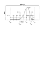
図3は、このように分割された一つの画素領域52に含まれる全画素の輝度における度数分布の一例を示す特性図である。この輝度の度数分布61において、陥没した欠陥部(例えば、ヘゲ、ブロ、縦割れ、耳ヒビなど)の輝度分布は輝度の低い範囲に分布する。これは、照明装置2により照明された光が陥没した欠陥部に吸収され、撮像装置3に受光されないことに起因する。一方、突出した欠陥部(例えば、バリ押し、絞りなど)の輝度分布61は、輝度の高い範囲に分布する。これは、照明装置2により照射された光が突出した欠陥部により正反射あるいはそれに近い状態で反射したことにより、撮像装置3に照度の高い光を受光したことに起因する。つまり、鋼板1の表面について欠陥53を検出するためには、基本的には、欠陥検出部45に対して輝度の度数分布61において上側閾値Toverと下側閾値Tunderとを適正に設定し、上側閾値Toverよりも輝度の高い範囲、下側閾値Tunderよりも輝度の低い範囲に含まれる画素を抽出することにより、欠陥53の検出が可能である。
FIG. 3 is a characteristic diagram showing an example of the frequency distribution in the luminance of all the pixels included in one
ここで、従来の欠陥検出技術としては、分割された画素領域の輝度における分散σ2を用いて、
上側閾値Tover=Lave+kσ2 (1)
下側閾値Tunder=Lave−kσ2 (2)
を設定し、欠陥の検出を行っていた。なお、Laveは平均輝度を示すLバーを意味するものとする(本明細書においては、以下同様とする)。また、kは所定の係数である。
Here, as a conventional defect detection technique, using the variance σ 2 in the luminance of the divided pixel region,
Upper threshold value T over = L ave + kσ 2 (1)
Lower threshold value T under = L ave −kσ 2 (2)
Was set to detect defects. Note that L ave means an L bar indicating the average luminance (the same shall apply hereinafter). K is a predetermined coefficient.
しかしながら、鋼板表面における輝度の度数分布は、平均輝度Laveに対して正規分布のような等方的な分布傾向とはならないため、分散σ2のみで上側閾値Toverと下側閾値Tunderとを設定した場合、鋼板表面の地合に不適合な閾値設定となってしまう。 However, since the luminance frequency distribution on the surface of the steel sheet does not have an isotropic distribution tendency like the normal distribution with respect to the average luminance L ave , the upper threshold value T over and the lower threshold value T under only with the variance σ 2. Is set to a threshold value that is incompatible with the formation of the steel sheet surface.
そこで、本実施の形態では、輝度の度数分布61が平均輝度Laveに対して等方的でない場合に、図3に示す上側閾値Toverと下側閾値Tunderとを、平均輝度Lave、最大輝度Lmax、最小輝度Lminを用いて、
上側閾値Tover=Lave+k´over|Lmax−Lave| (3)
下側閾値Tunder=Lave −k´under|Lmin−Lave| (4)
(k´over、k´underは、所定の係数である)
と設定することにより、鋼板1の表面における輝度の度数分布61を反映した閾値設定を可能としたものである。ここで、このような上側閾値Toverと下側閾値Tunderとの自動設定を行うため、係数k´over、k´underを目視検査の判定結果に適合した値に設定する。
Therefore, in this embodiment, when the frequency distribution 61 of the intensity is not isotropic with respect to the average luminance L ave, an upper threshold value T-over-the lower threshold T under shown in FIG. 3, the average luminance L ave, Using the maximum brightness L max and the minimum brightness L min ,
Upper threshold T over = L ave + k ′ over | L max −L ave | (3)
Lower threshold T under = L ave - k'under | L min -L ave | (4)
(K'over, k'under are predetermined coefficients)
Thus, the threshold value setting that reflects the luminance frequency distribution 61 on the surface of the
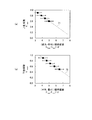
このため、まず、平均輝度Lave、標準偏差輝度σ、最大輝度Lmax、最小輝度Lminを用いて特徴量|Lave−Lmax|÷σおよび|Lave−Lmin|÷σを算出する。ここで、度数の分布にはバラツキがあるので、標準偏差輝度σは、正規分布にフィッティングした後の値が用いられる。そして、目視検査により得られる閾値における係数k´over、k´underと算出された特徴量|Lave−Lmax|÷σ、|Lave−Lmin|÷σとの相関を求めて、直線近似することにより、
k´over=α|Lave−Lmax|÷σ+β (5)
k´under=α´|Lave−Lmin|÷σ+β´ (6)
(α、β、α´、β´は任意の定数である)
なる関係式が得られたものである。
For this reason, first, the feature quantities | L ave −L max | ÷ σ and | L ave −L min | ÷ σ are calculated using the average luminance L ave , the standard deviation luminance σ, the maximum luminance L max , and the minimum luminance L min. To do. Here, since the frequency distribution varies, the standard deviation luminance σ is a value after fitting to the normal distribution. Then, the coefficients k ′ over and k ′ under at the threshold values obtained by visual inspection and the calculated feature quantities | L ave −L max | ÷ σ and | L ave −L min | ÷ σ are obtained to obtain a straight line By approximating
k ′ over = α | L ave −L max | ÷ σ + β (5)
k ′ under = α ′ | L ave −L min | ÷ σ + β ′ (6)
(Α, β, α ′, β ′ are arbitrary constants)
The following relational expression is obtained.
図4は、上側係数k´over、下側係数k´underと特徴量|Lave−Lmax|÷σ、|Lave−Lmin|÷σとの相関の一例を示す特性図である。本実施の形態では、このように目視検査による上側係数k´over、下側係数k´underと特徴量|Lave−Lmax|÷σ、|Lave−Lmin|÷σとの間には所定の相関関係があることを見出したものであり、図示例では、(5)式の関係式を示す直線71の相関係数は、α=−0.97、(6)式の関係式を示す直線72の相関係数は、α´=−0.97となったものである。相関テーブル44は、目視検査の結果に基づくこのような上側係数k´over、下側係数k´underと特徴量|Lave−Lmax|÷σ、|Lave−Lmin|÷σとの相関関係を予め記憶したメモリである。
FIG. 4 is a characteristic diagram illustrating an example of the correlation between the upper coefficient k ′ over , the lower coefficient k ′ under, and the feature quantities | L ave −L max | ÷ σ and | L ave −L min | ÷ σ. In this embodiment, the upper coefficient k ′ over and the lower coefficient k ′ under by visual inspection and the feature quantities | L ave −L max | ÷ σ and | L ave −L min | ÷ σ Has been found to have a predetermined correlation. In the illustrated example, the correlation coefficient of the
そこで、本実施の形態では、欠陥検出に際して、まず、特徴量算出部42により、画素領域52毎に、平均輝度Lave、標準偏差輝度σ、最大輝度Lmax、最小輝度Lminを用いて特徴量|Lave−Lmax|÷σおよび|Lave−Lmin|÷σを算出する。そして、閾値設定部43は、算出された特徴量|Lave−Lmax|÷σおよび|Lave−Lmin|÷σを用いて相関テーブル44を参照し、関係式(5),(3)、(6),(4)を各々用いることにより、上側閾値Toverと下側閾値Tunderとを算出して欠陥検出部45に対して自動設定する。
Therefore, in the present embodiment, when detecting a defect, first, the feature
これにより、鋼板1の表面の地合の変動に適合した上側閾値Tover、下側閾値Tunderの設定が可能となり、地合の変動の大きい鋼板1においても、目視検査に近い欠陥53の検出が可能となる。特に、本実施の形態では、フレーム画像について分割された画素領域52毎に各々の処理を実行するようにしているので、局所的に地合の変動が大きい場合でも、局所的な地合の変動が大きい領域に対応した適正な上側閾値Tover、下側閾値Tunderの設定が可能となる。
Accordingly, it is possible to set the upper threshold value T over and the lower threshold value T under suitable for the fluctuation of the surface condition of the
図5は、変形例の画像処理装置4の構成例を示す概略ブロック図である。本実施の形態では、画像分割部41により1種類のサイズの画素領域52に分割するようにしたが、図5に示すように、撮像により得られた一つのフレーム画像に対して画像分割部41a、41bの並行処理により異なるサイズA,Bの画素領域52として各々複数に分割するようにしてもよい。図6は、異なるサイズA,Bによるフレーム画像の分割例を示す説明図である。
FIG. 5 is a schematic block diagram illustrating a configuration example of the
そして、特徴量算出部42a、42bおよび閾値設定部43a、43bを用いて、分割された異なるサイズA,Bの画素領域52毎に各々の処理を並行して実行する。さらに、欠陥検出部45では、分割された異なるサイズA,Bの画素領域52毎に欠陥候補抽出部45a、45bにより各々上側閾値Tover、下側閾値Tunderを用いて該当する画素の集まりを欠陥53の候補として抽出し、このような異なる分割サイズA,Bによる処理結果を最終的に欠陥検出部45cにおいて選択信号に応じて選択的に用いるようにする。すなわち、検出したい欠陥に対応する選択信号に応じて、分割サイズAによる処理結果を用いたり、分割サイズBによる処理結果を用いたり、分割サイズA,B双方による処理結果を用いたりすればよい。
Then, using the feature
なお、分割サイズAは、図6(a)に示すように、図2に示したサイズと同じであり、たとえば主走査方向Xが27.5mmであり、副走査方向Yが110mmである。これに対し、分割サイズBは、図6(b)に示すように、分割サイズAを主走査方向Xに8倍広げたサイズであり、たとえば主走査方向Xが220mmであり、副走査方向Yが110mmである。 As shown in FIG. 6A, the division size A is the same as the size shown in FIG. 2, for example, the main scanning direction X is 27.5 mm and the sub-scanning direction Y is 110 mm. On the other hand, as shown in FIG. 6B, the division size B is a size obtained by expanding the division size A eight times in the main scanning direction X. For example, the main scanning direction X is 220 mm, and the sub-scanning direction Y Is 110 mm.
これにより、特定の欠陥種(例えば、ヘゲ、しぼり、ブロなど)において検出率が向上する画素領域52のサイズがあった場合に、欠陥検出としてそのサイズの処理結果を優先的に認めることにより、欠陥の検出効率が向上することとなる。したがって、選択信号としては、例えば異常形状情報などを用いればよく、例えば異常形状情報が「大」の場合には、分割サイズB側の処理結果を用い、異常形状情報が「小」の場合には、分割サイズA側の処理結果を用いるようにすればよい。
Thereby, when there is a size of the
たとえば、分割サイズAは、欠陥面積の小さいヘゲや耳ヒビなどの欠陥に対する検出効率がよく、分割サイズBは、副走査方向Yに延びる頻度が高いブロなどの欠陥に対する検出効率がよい。すなわち、分割サイズは、分割サイズ面積に対する欠陥面積の比が所定値以下となるようにするのが好ましい。また、この際、ブロなどのように、欠陥の形状を考慮して主走査方向Xと副走査方向Yとの値を決定するとよい。 For example, the division size A has good detection efficiency for defects such as baldness and ear cracks with a small defect area, and the division size B has good detection efficiency for defects such as blow that frequently extend in the sub-scanning direction Y. That is, it is preferable that the division size is such that the ratio of the defect area to the division size area is a predetermined value or less. At this time, the values of the main scanning direction X and the sub-scanning direction Y may be determined in consideration of the shape of the defect, such as a blow.
なお、図4では、目視検査により得られる閾値における係数k´over、k´underと算出された特徴量|Lave−Lmax|÷σ、|Lave−Lmin|÷σとの相関関係を直線近似による関係式として求めていたが、これに限らず、他の曲線近似、たとえば多項式近似などの関係式であってもよい。 In FIG. 4, the correlation between the coefficients k ′ over and k ′ under at the threshold values obtained by visual inspection and the calculated feature quantities | L ave −L max | ÷ σ, | L ave −L min | ÷ σ. However, the present invention is not limited to this, and may be a relational expression such as another curve approximation, for example, a polynomial approximation.
1 鋼板
3 撮像装置
41 画像分割部
42 特徴量算出部
43 閾値設定部
45 欠陥検出部
DESCRIPTION OF
Claims (10)
撮像により得られた画像における平均輝度、標準偏差輝度、および最大輝度に基づき、該画像の輝度の度数分布についての第1特徴量を算出し、撮像により得られた画像における平均輝度、標準偏差輝度、および最小輝度に基づき、該画像の輝度の度数分布についての第2特徴量を算出する特徴量算出手段と、
算出された第1特徴量を用いて算出した上側所定係数と平均輝度と最大輝度とに基づき輝度の上側閾値を設定し、算出された第2特徴量を用いて算出した下側所定係数と平均輝度と最小輝度とに基づき輝度の下側閾値を設定する閾値設定手段と、
設定された上側閾値および下側閾値に基づき撮像により得られた前記画像における欠陥画素を検出する欠陥検出手段と、
を備えることを特徴とする表面欠陥検出装置。 Imaging means for imaging the illuminated surface to be inspected;
Based on the average luminance, standard deviation luminance, and maximum luminance in the image obtained by imaging, the first feature amount for the frequency distribution of the luminance of the image is calculated, and the average luminance and standard deviation luminance in the image obtained by imaging are calculated. And a feature amount calculating means for calculating a second feature amount for the frequency distribution of the brightness of the image based on the minimum brightness,
An upper threshold value of luminance is set based on the upper predetermined coefficient calculated using the calculated first feature value, the average luminance, and the maximum luminance, and the lower predetermined coefficient calculated using the calculated second feature value and the average Threshold setting means for setting a lower threshold of the luminance based on the luminance and the minimum luminance;
Defect detection means for detecting defective pixels in the image obtained by imaging based on the set upper threshold and lower threshold;
A surface defect detection apparatus comprising:
前記特徴量算出手段、前記閾値設定手段および前記欠陥検出手段は、分割された画素領域毎に各々の処理を実行することを特徴とする請求項1または2に記載の表面欠陥検出装置。 Image division means for dividing an image obtained by imaging into a plurality of pixel regions arranged in parallel in the vertical and horizontal directions;
The surface defect detection apparatus according to claim 1, wherein the feature amount calculation unit, the threshold value setting unit, and the defect detection unit execute respective processes for each divided pixel region.
前記特徴量算出手段および前記閾値設定手段は、分割された異なるサイズの画素領域毎に各々の処理を並行して実行し、
前記欠陥検出手段は、異なる分割サイズによる処理結果を選択的に用いて処理を実行することを特徴とする請求項3に記載の表面欠陥検出装置。 The image dividing means divides a single image obtained by imaging into a plurality of pixel regions of different sizes by parallel processing,
The feature amount calculating means and the threshold value setting means execute each process in parallel for each divided pixel area of different size,
The surface defect detection apparatus according to claim 3, wherein the defect detection unit performs processing by selectively using processing results of different division sizes.
前記第2特徴量は、|平均輝度−最小輝度|÷標準偏差輝度であることを特徴とする請求項1〜4のいずれか一つに記載の表面欠陥検出装置。 The first feature amount is | average luminance−maximum luminance | ÷ standard deviation luminance.
5. The surface defect detection apparatus according to claim 1, wherein the second feature amount is | average luminance−minimum luminance | ÷ standard deviation luminance.
撮像により得られた画像における平均輝度、標準偏差輝度、および最大輝度に基づき、該画像の輝度の度数分布についての第1特徴量を算出し、撮像により得られた画像における平均輝度、標準偏差輝度、および最小輝度に基づき、該画像の輝度の度数分布についての第2特徴量を算出する特徴量算出ステップと、
算出された第1特徴量を用いて算出した上側所定係数と平均輝度と最大輝度とに基づき輝度の上側閾値を設定し、算出された第2特徴量を用いて算出した下側所定係数と平均輝度と最小輝度とに基づき輝度の下側閾値を設定する閾値設定ステップと、
設定された上側閾値および下側閾値に基づき撮像により得られた前記画像における欠陥画素を検出する欠陥検出ステップと、
を含むことを特徴とする表面欠陥検出方法。 An imaging step of imaging the illuminated surface to be inspected by an imaging means;
Based on the average luminance, standard deviation luminance, and maximum luminance in the image obtained by imaging, the first feature amount for the frequency distribution of the luminance of the image is calculated, and the average luminance and standard deviation luminance in the image obtained by imaging are calculated. And a feature amount calculating step for calculating a second feature amount for the frequency distribution of the brightness of the image based on the minimum brightness;
An upper threshold value of luminance is set based on the upper predetermined coefficient calculated using the calculated first feature value, the average luminance, and the maximum luminance, and the lower predetermined coefficient calculated using the calculated second feature value and the average A threshold setting step for setting a lower threshold of the luminance based on the luminance and the minimum luminance;
A defect detection step of detecting defective pixels in the image obtained by imaging based on the set upper threshold and lower threshold;
A method for detecting surface defects, comprising:
前記特徴量算出ステップ、前記閾値設定ステップおよび前記欠陥検出ステップは、分割された画素領域毎に各々の処理を実行することを特徴とする請求項6または7に記載の表面欠陥検出方法。 Further comprising an image dividing step of dividing an image obtained by imaging into a plurality of pixel regions arranged in parallel vertically and horizontally;
8. The surface defect detection method according to claim 6, wherein the feature amount calculation step, the threshold value setting step, and the defect detection step execute respective processes for each divided pixel region.
前記特徴量算出ステップおよび前記閾値設定ステップは、分割された異なるサイズの画素領域毎に各々の処理を並行して実行し、
前記欠陥検出ステップは、異なる分割サイズによる処理結果を選択的に用いて処理を実行することを特徴とする請求項8に記載の表面欠陥検出方法。 In the image dividing step, one image obtained by imaging is divided into a plurality of pixel region groups having different sizes by parallel processing,
The feature amount calculation step and the threshold value setting step execute each process in parallel for each of the divided pixel areas of different sizes,
9. The surface defect detection method according to claim 8, wherein in the defect detection step, the processing is executed by selectively using a processing result with a different division size.
前記第2特徴量は、|平均輝度−最小輝度|÷標準偏差輝度であることを特徴とする請求項6〜9のいずれか一つに記載の表面欠陥検出方法。 The first feature amount is | average luminance−maximum luminance | ÷ standard deviation luminance.
10. The surface defect detection method according to claim 6, wherein the second feature amount is | average luminance−minimum luminance | ÷ standard deviation luminance.
Priority Applications (1)
| Application Number | Priority Date | Filing Date | Title |
|---|---|---|---|
| JP2011018729A JP5849397B2 (en) | 2011-01-31 | 2011-01-31 | Surface defect detection device and surface defect detection method |
Applications Claiming Priority (1)
| Application Number | Priority Date | Filing Date | Title |
|---|---|---|---|
| JP2011018729A JP5849397B2 (en) | 2011-01-31 | 2011-01-31 | Surface defect detection device and surface defect detection method |
Publications (2)
| Publication Number | Publication Date |
|---|---|
| JP2012159376A JP2012159376A (en) | 2012-08-23 |
| JP5849397B2 true JP5849397B2 (en) | 2016-01-27 |
Family
ID=46840043
Family Applications (1)
| Application Number | Title | Priority Date | Filing Date |
|---|---|---|---|
| JP2011018729A Expired - Fee Related JP5849397B2 (en) | 2011-01-31 | 2011-01-31 | Surface defect detection device and surface defect detection method |
Country Status (1)
| Country | Link |
|---|---|
| JP (1) | JP5849397B2 (en) |
Families Citing this family (7)
| Publication number | Priority date | Publication date | Assignee | Title |
|---|---|---|---|---|
| JP6905844B2 (en) * | 2017-03-28 | 2021-07-21 | 株式会社ミツトヨ | Hardness tester and program |
| CN109085248B (en) * | 2018-07-03 | 2021-04-06 | 内蒙古科技大学 | Method, device and system for locating impact source of pressure-bearing pipeline wall |
| WO2020202496A1 (en) | 2019-04-03 | 2020-10-08 | 日本電気株式会社 | Surface abnormality detection device and system |
| CN110400306B (en) * | 2019-07-29 | 2023-05-23 | 恒天嘉华非织造有限公司 | Non-woven fabric defect detection method based on morphological filtering and convolutional neural network |
| CN111833350B (en) * | 2020-08-26 | 2023-06-06 | 南京原觉信息科技有限公司 | Machine vision detection method and system |
| CN114821195B (en) * | 2022-06-01 | 2022-12-16 | 南阳师范学院 | Computer Image Intelligent Recognition Method |
| CN120495217B (en) * | 2025-05-06 | 2026-01-23 | 徐州远翔机车科技有限公司 | A method and system for detecting scratches on the surface of steel wheels |
Family Cites Families (4)
| Publication number | Priority date | Publication date | Assignee | Title |
|---|---|---|---|---|
| JP4254323B2 (en) * | 2003-04-18 | 2009-04-15 | 株式会社デンソー | Foreign matter inspection method and foreign matter inspection device |
| JP4399494B2 (en) * | 2006-12-28 | 2010-01-13 | シャープ株式会社 | Defect detection apparatus, defect detection method, image sensor device, and image sensor module |
| JP5050533B2 (en) * | 2007-01-24 | 2012-10-17 | 凸版印刷株式会社 | EXPOSURE METHOD, EXPOSURE APPARATUS, AND COLOR FILTER MANUFACTURING METHOD |
| JP5659540B2 (en) * | 2009-04-15 | 2015-01-28 | Jfeスチール株式会社 | Steel plate surface defect inspection method and apparatus |
-
2011
- 2011-01-31 JP JP2011018729A patent/JP5849397B2/en not_active Expired - Fee Related
Also Published As
| Publication number | Publication date |
|---|---|
| JP2012159376A (en) | 2012-08-23 |
Similar Documents
| Publication | Publication Date | Title |
|---|---|---|
| JP5849397B2 (en) | Surface defect detection device and surface defect detection method | |
| CN110431404B (en) | Surface defect inspection method and surface defect inspection device | |
| CN101256157B (en) | Surface defect detection method and device | |
| CN111294589B (en) | Camera module lens surface detection method | |
| CN115239704B (en) | Accurate detection and repair method for wood surface defects | |
| CN103760165B (en) | The defect inspection method of display floater and defect detecting device | |
| CN107301637B (en) | Surface defect detection method for nearly rectangular planar industrial products | |
| JP6027295B1 (en) | Surface defect inspection apparatus and surface defect inspection method for hot dip galvanized steel sheet | |
| SG164293A1 (en) | System and method for inspecting a wafer | |
| KR101862310B1 (en) | Apparatus and Method for Detecting Mura Defects | |
| JP2007132757A (en) | Appearance inspection method and apparatus | |
| JP2008267943A (en) | Crack detection method | |
| JP3913517B2 (en) | Defect detection method | |
| JP2004219291A (en) | Screen line defect detection method and apparatus | |
| KR101562988B1 (en) | Apparatus and method for detecting surface defects of hot billet | |
| JP2008020235A5 (en) | ||
| KR20110020437A (en) | Defect inspection method of patterned wafer | |
| CN108280825A (en) | A kind of liquid crystal display emargintion detection method | |
| JP2014135007A (en) | Flat panel display automatic unevenness detection device and automatic unevenness detection method | |
| JP2004219072A (en) | Screen streak defect detection method and device | |
| JP3015325B2 (en) | Streak inspection method and device | |
| WO2024070101A1 (en) | Surface defect detecting method and surface defect detecting device | |
| CN116843640A (en) | Method, system and storage medium for detecting pit defects on ceramic tile surface | |
| TWI456185B (en) | Water turbidity detection system and the method thereof | |
| CN102982554A (en) | Image edge detection method and device |
Legal Events
| Date | Code | Title | Description |
|---|---|---|---|
| A621 | Written request for application examination |
Free format text: JAPANESE INTERMEDIATE CODE: A621 Effective date: 20140115 |
|
| A977 | Report on retrieval |
Free format text: JAPANESE INTERMEDIATE CODE: A971007 Effective date: 20140618 |
|
| A131 | Notification of reasons for refusal |
Free format text: JAPANESE INTERMEDIATE CODE: A131 Effective date: 20150106 |
|
| A521 | Written amendment |
Free format text: JAPANESE INTERMEDIATE CODE: A523 Effective date: 20150304 |
|
| A131 | Notification of reasons for refusal |
Free format text: JAPANESE INTERMEDIATE CODE: A131 Effective date: 20150825 |
|
| A521 | Written amendment |
Free format text: JAPANESE INTERMEDIATE CODE: A523 Effective date: 20151015 |
|
| TRDD | Decision of grant or rejection written | ||
| A01 | Written decision to grant a patent or to grant a registration (utility model) |
Free format text: JAPANESE INTERMEDIATE CODE: A01 Effective date: 20151104 |
|
| A61 | First payment of annual fees (during grant procedure) |
Free format text: JAPANESE INTERMEDIATE CODE: A61 Effective date: 20151117 |
|
| R150 | Certificate of patent or registration of utility model |
Ref document number: 5849397 Country of ref document: JP Free format text: JAPANESE INTERMEDIATE CODE: R150 |
|
| LAPS | Cancellation because of no payment of annual fees |