JP5833988B2 - Removal of aluminum nitride part - Google Patents
Removal of aluminum nitride part Download PDFInfo
- Publication number
- JP5833988B2 JP5833988B2 JP2012171055A JP2012171055A JP5833988B2 JP 5833988 B2 JP5833988 B2 JP 5833988B2 JP 2012171055 A JP2012171055 A JP 2012171055A JP 2012171055 A JP2012171055 A JP 2012171055A JP 5833988 B2 JP5833988 B2 JP 5833988B2
- Authority
- JP
- Japan
- Prior art keywords
- substrate
- subassembly
- light
- aln
- layer
- Prior art date
- Legal status (The legal status is an assumption and is not a legal conclusion. Google has not performed a legal analysis and makes no representation as to the accuracy of the status listed.)
- Active
Links
- PMHQVHHXPFUNSP-UHFFFAOYSA-M copper(1+);methylsulfanylmethane;bromide Chemical group Br[Cu].CSC PMHQVHHXPFUNSP-UHFFFAOYSA-M 0.000 title claims description 149
- 239000000758 substrate Substances 0.000 claims description 205
- 238000000034 method Methods 0.000 claims description 81
- 238000005530 etching Methods 0.000 claims description 62
- 230000008569 process Effects 0.000 claims description 58
- 238000005259 measurement Methods 0.000 claims description 18
- 239000000126 substance Substances 0.000 claims description 12
- 230000004044 response Effects 0.000 claims description 5
- 230000003595 spectral effect Effects 0.000 claims description 3
- NBIIXXVUZAFLBC-UHFFFAOYSA-N Phosphoric acid Chemical compound OP(O)(O)=O NBIIXXVUZAFLBC-UHFFFAOYSA-N 0.000 description 28
- 229910002704 AlGaN Inorganic materials 0.000 description 21
- 229910000147 aluminium phosphate Inorganic materials 0.000 description 14
- 230000007547 defect Effects 0.000 description 13
- 238000010586 diagram Methods 0.000 description 13
- 238000012545 processing Methods 0.000 description 12
- 239000013078 crystal Substances 0.000 description 11
- 229910052782 aluminium Inorganic materials 0.000 description 10
- XAGFODPZIPBFFR-UHFFFAOYSA-N aluminium Chemical compound [Al] XAGFODPZIPBFFR-UHFFFAOYSA-N 0.000 description 10
- 239000000463 material Substances 0.000 description 10
- 230000008859 change Effects 0.000 description 8
- 230000009467 reduction Effects 0.000 description 8
- 238000009835 boiling Methods 0.000 description 7
- 230000003287 optical effect Effects 0.000 description 7
- 239000000523 sample Substances 0.000 description 7
- 230000007704 transition Effects 0.000 description 7
- 238000013461 design Methods 0.000 description 6
- 239000002253 acid Substances 0.000 description 5
- 238000002347 injection Methods 0.000 description 5
- 239000007924 injection Substances 0.000 description 5
- 239000000243 solution Substances 0.000 description 5
- XLYOFNOQVPJJNP-UHFFFAOYSA-N water Substances O XLYOFNOQVPJJNP-UHFFFAOYSA-N 0.000 description 5
- PIGFYZPCRLYGLF-UHFFFAOYSA-N Aluminum nitride Chemical compound [Al]#N PIGFYZPCRLYGLF-UHFFFAOYSA-N 0.000 description 4
- 230000007062 hydrolysis Effects 0.000 description 4
- 238000006460 hydrolysis reaction Methods 0.000 description 4
- 239000013307 optical fiber Substances 0.000 description 4
- 238000002441 X-ray diffraction Methods 0.000 description 3
- 230000004888 barrier function Effects 0.000 description 3
- 230000005540 biological transmission Effects 0.000 description 3
- 230000005670 electromagnetic radiation Effects 0.000 description 3
- 150000002500 ions Chemical class 0.000 description 3
- 229910052751 metal Inorganic materials 0.000 description 3
- 239000002184 metal Substances 0.000 description 3
- 239000000203 mixture Substances 0.000 description 3
- 230000005693 optoelectronics Effects 0.000 description 3
- 230000003746 surface roughness Effects 0.000 description 3
- IJGRMHOSHXDMSA-UHFFFAOYSA-N Atomic nitrogen Chemical compound N#N IJGRMHOSHXDMSA-UHFFFAOYSA-N 0.000 description 2
- 239000000956 alloy Substances 0.000 description 2
- 229910045601 alloy Inorganic materials 0.000 description 2
- 238000013459 approach Methods 0.000 description 2
- 230000008901 benefit Effects 0.000 description 2
- 230000015572 biosynthetic process Effects 0.000 description 2
- 230000000903 blocking effect Effects 0.000 description 2
- 238000003486 chemical etching Methods 0.000 description 2
- 238000005229 chemical vapour deposition Methods 0.000 description 2
- 238000005253 cladding Methods 0.000 description 2
- 238000000605 extraction Methods 0.000 description 2
- 150000004678 hydrides Chemical class 0.000 description 2
- 238000011065 in-situ storage Methods 0.000 description 2
- 239000010453 quartz Substances 0.000 description 2
- HBMJWWWQQXIZIP-UHFFFAOYSA-N silicon carbide Chemical compound [Si+]#[C-] HBMJWWWQQXIZIP-UHFFFAOYSA-N 0.000 description 2
- 229910010271 silicon carbide Inorganic materials 0.000 description 2
- VYPSYNLAJGMNEJ-UHFFFAOYSA-N silicon dioxide Inorganic materials O=[Si]=O VYPSYNLAJGMNEJ-UHFFFAOYSA-N 0.000 description 2
- 238000007740 vapor deposition Methods 0.000 description 2
- 238000001039 wet etching Methods 0.000 description 2
- 230000004913 activation Effects 0.000 description 1
- 238000001816 cooling Methods 0.000 description 1
- 238000005520 cutting process Methods 0.000 description 1
- 230000007423 decrease Effects 0.000 description 1
- 230000003111 delayed effect Effects 0.000 description 1
- 238000007598 dipping method Methods 0.000 description 1
- 238000004090 dissolution Methods 0.000 description 1
- 238000009826 distribution Methods 0.000 description 1
- 230000005684 electric field Effects 0.000 description 1
- 238000000572 ellipsometry Methods 0.000 description 1
- 239000007943 implant Substances 0.000 description 1
- 239000012535 impurity Substances 0.000 description 1
- 229910052738 indium Inorganic materials 0.000 description 1
- APFVFJFRJDLVQX-UHFFFAOYSA-N indium atom Chemical compound [In] APFVFJFRJDLVQX-UHFFFAOYSA-N 0.000 description 1
- 238000005305 interferometry Methods 0.000 description 1
- 238000010884 ion-beam technique Methods 0.000 description 1
- 238000011326 mechanical measurement Methods 0.000 description 1
- 238000012544 monitoring process Methods 0.000 description 1
- 150000004767 nitrides Chemical class 0.000 description 1
- 229910052757 nitrogen Inorganic materials 0.000 description 1
- 230000010287 polarization Effects 0.000 description 1
- 238000005498 polishing Methods 0.000 description 1
- NTTOTNSKUYCDAV-UHFFFAOYSA-N potassium hydride Chemical compound [KH] NTTOTNSKUYCDAV-UHFFFAOYSA-N 0.000 description 1
- 229910000105 potassium hydride Inorganic materials 0.000 description 1
- 230000001902 propagating effect Effects 0.000 description 1
- 238000010992 reflux Methods 0.000 description 1
- 230000000717 retained effect Effects 0.000 description 1
- 229910052594 sapphire Inorganic materials 0.000 description 1
- 239000010980 sapphire Substances 0.000 description 1
- 230000035945 sensitivity Effects 0.000 description 1
- 229910052710 silicon Inorganic materials 0.000 description 1
- 239000010703 silicon Substances 0.000 description 1
- 238000000927 vapour-phase epitaxy Methods 0.000 description 1
Images


Classifications
-
- H—ELECTRICITY
- H01—ELECTRIC ELEMENTS
- H01L—SEMICONDUCTOR DEVICES NOT COVERED BY CLASS H10
- H01L22/00—Testing or measuring during manufacture or treatment; Reliability measurements, i.e. testing of parts without further processing to modify the parts as such; Structural arrangements therefor
- H01L22/20—Sequence of activities consisting of a plurality of measurements, corrections, marking or sorting steps
- H01L22/26—Acting in response to an ongoing measurement without interruption of processing, e.g. endpoint detection, in-situ thickness measurement
-
- H—ELECTRICITY
- H01—ELECTRIC ELEMENTS
- H01L—SEMICONDUCTOR DEVICES NOT COVERED BY CLASS H10
- H01L21/00—Processes or apparatus adapted for the manufacture or treatment of semiconductor or solid state devices or of parts thereof
- H01L21/67—Apparatus specially adapted for handling semiconductor or electric solid state devices during manufacture or treatment thereof; Apparatus specially adapted for handling wafers during manufacture or treatment of semiconductor or electric solid state devices or components ; Apparatus not specifically provided for elsewhere
- H01L21/67005—Apparatus not specifically provided for elsewhere
- H01L21/67011—Apparatus for manufacture or treatment
- H01L21/67017—Apparatus for fluid treatment
- H01L21/67063—Apparatus for fluid treatment for etching
- H01L21/67075—Apparatus for fluid treatment for etching for wet etching
- H01L21/67086—Apparatus for fluid treatment for etching for wet etching with the semiconductor substrates being dipped in baths or vessels
-
- H—ELECTRICITY
- H01—ELECTRIC ELEMENTS
- H01L—SEMICONDUCTOR DEVICES NOT COVERED BY CLASS H10
- H01L21/00—Processes or apparatus adapted for the manufacture or treatment of semiconductor or solid state devices or of parts thereof
- H01L21/67—Apparatus specially adapted for handling semiconductor or electric solid state devices during manufacture or treatment thereof; Apparatus specially adapted for handling wafers during manufacture or treatment of semiconductor or electric solid state devices or components ; Apparatus not specifically provided for elsewhere
- H01L21/67005—Apparatus not specifically provided for elsewhere
- H01L21/67242—Apparatus for monitoring, sorting or marking
- H01L21/67253—Process monitoring, e.g. flow or thickness monitoring
-
- H—ELECTRICITY
- H01—ELECTRIC ELEMENTS
- H01L—SEMICONDUCTOR DEVICES NOT COVERED BY CLASS H10
- H01L22/00—Testing or measuring during manufacture or treatment; Reliability measurements, i.e. testing of parts without further processing to modify the parts as such; Structural arrangements therefor
- H01L22/10—Measuring as part of the manufacturing process
- H01L22/12—Measuring as part of the manufacturing process for structural parameters, e.g. thickness, line width, refractive index, temperature, warp, bond strength, defects, optical inspection, electrical measurement of structural dimensions, metallurgic measurement of diffusions
-
- H—ELECTRICITY
- H01—ELECTRIC ELEMENTS
- H01L—SEMICONDUCTOR DEVICES NOT COVERED BY CLASS H10
- H01L33/00—Semiconductor devices with at least one potential-jump barrier or surface barrier specially adapted for light emission; Processes or apparatus specially adapted for the manufacture or treatment thereof or of parts thereof; Details thereof
- H01L33/005—Processes
- H01L33/0093—Wafer bonding; Removal of the growth substrate
Description
本発明は、窒化アルミニウム部分を実質的に除去または薄膜化する方法に関し、より詳細には、この部分を約50μm未満の厚さまで完全に除去するかまたは化学的に薄膜化する方法に関する。また、本発明の装置は、エッチング処理中にエッチング液にバルク窒化アルミニウム(AlN)基板をさらすように構成されたチャンバを含む。 The present invention relates to a method for substantially removing or thinning an aluminum nitride portion, and more particularly to a method for completely removing or chemically thinning this portion to a thickness of less than about 50 μm. The apparatus of the present invention also includes a chamber configured to expose a bulk aluminum nitride (AlN) substrate to an etchant during the etching process.
本発明は、窒化アルミニウム部分を実質的に除去または薄膜化する方法に関し、より詳細には、この部分を約50μm未満の厚さまで完全に除去するかまたは化学的に薄膜化する方法に関する。また、本発明の装置は、エッチング処理中にエッチング液にバルク窒化アルミニウム(AlN)基板をさらすように構成されたチャンバを含む。 The present invention relates to a method for substantially removing or thinning an aluminum nitride portion, and more particularly to a method for completely removing or chemically thinning this portion to a thickness of less than about 50 μm. The apparatus of the present invention also includes a chamber configured to expose a bulk aluminum nitride (AlN) substrate to an etchant during the etching process.
このバルクAlN基板は、このバルクAlN基板上に成長した1層以上のエピタキシャル層を含むサブアセンブリから成る基板である。この装置は、バルクAlN基板の厚さを示す信号を生成するように構成された計測ユニットも含む。 The bulk AlN substrate is a substrate composed of a subassembly including one or more epitaxial layers grown on the bulk AlN substrate. The apparatus also includes a metrology unit configured to generate a signal indicative of the thickness of the bulk AlN substrate.
また、本発明は、バルクAlN基板上に成長した1層以上のエピタキシャル層を含むサブアセンブリからバルク窒化アルミニウム(AlN)基板を実質的に除去する方法に関する。AlN基板をエッチング処理中にエッチング液にさらす。AlN基の厚さを測定し、AlN基板の測定された厚さに基づいてエッチング処理を必要に応じて調整する。 The present invention also relates to a method for substantially removing a bulk aluminum nitride (AlN) substrate from a subassembly including one or more epitaxial layers grown on the bulk AlN substrate. The AlN substrate is exposed to an etchant during the etching process. The thickness of the AlN group is measured, and the etching process is adjusted as necessary based on the measured thickness of the AlN substrate.
バルク結晶AlN基板は、種結晶から単結晶AlNボウルを成長させ、ボウルをウエハ基板にスライスすることによって形成される。材料の層、例えば、実質的にバルクAlN基板に格子整合されたIII族窒化物材料を、本明細書中に説明されているサブアセンブリを形成するために、高結晶質を有するウエハ基板上にエピタキシャル成長させてよい。サブアセンブリ層は、エピタキシャル成長の初期表面であるバルクAlN基板に最も近い表面を有している。バルクAlN基板を除去した後、エピタキシャル成長層は、バルク結晶AlN基板と実質的な格子整合によってエピタキシャル成長の初期表面の近傍で低い欠陥密度を有することができる。例えば、エピタキシャル層の欠陥密度は、108cm−3より低いかまたはエピタキシャル成長の初期表面の約100nm以内で約1010cm−3〜約103cm−3の範囲であってよい。エピタキシャル層の欠陥密度は、基板の欠陥密度に関連し得る。例えば、エピタキシャル層の欠陥密度は、基板の欠陥密度の約10〜約1000倍の範囲であってよい。 A bulk crystal AlN substrate is formed by growing a single crystal AlN bowl from a seed crystal and slicing the bowl into a wafer substrate. A layer of material, such as a III-nitride material substantially lattice matched to a bulk AlN substrate, is formed on a highly crystalline wafer substrate to form a subassembly as described herein. It may be epitaxially grown. The subassembly layer has a surface closest to the bulk AlN substrate, which is the initial surface for epitaxial growth. After removing the bulk AlN substrate, the epitaxial growth layer can have a low defect density near the initial surface of the epitaxial growth due to substantial lattice matching with the bulk crystal AlN substrate. For example, the defect density of the epitaxial layer may be less than 10 8 cm −3 or in the range of about 10 10 cm −3 to about 10 3 cm −3 within about 100 nm of the initial surface of the epitaxial growth. The defect density of the epitaxial layer can be related to the defect density of the substrate. For example, the defect density of the epitaxial layer may range from about 10 to about 1000 times the defect density of the substrate.
基板の実質的な除去は、エピタキシャル成長の初期表面の大部分に対して基板を除去する工程を含む。基板の実質的な除去は、たとえば、エピタキシャル成長の初期表面の大部分に対して化学的にエッチングすることにより、AlN基板を薄膜化する工程を含む。場合により、基板残部は、エッチング処理後のエピタキシャル成長の初期表面の大部分に対して残留する。基板残部は、約50μm〜0nm(完全に除去)または約50μm未満の厚さを有する。 Substantial removal of the substrate includes removing the substrate for most of the initial surface of the epitaxial growth. Substantial removal of the substrate involves thinning the AlN substrate, for example by chemically etching most of the initial surface of the epitaxial growth. In some cases, the remainder of the substrate remains over most of the initial surface of the epitaxial growth after the etching process. The remainder of the substrate has a thickness of about 50 μm to 0 nm (completely removed) or less than about 50 μm.
バルクAlN基板は、この材料における色中心、不純物、および他の欠陥により、ある波長範囲、たとえば、365nm以上の波長に対して、および/または、約200nm〜約365nmのUV波長範囲において実質的に光吸収性である。発光素子の場合、バルクAlN基板の実質的な除去によって素子の基板側(本明細書中では素子の裏面として示す)、すなわち、このバルクAlNが実質的に除去された表面を介して光を射出することが可能となる。バルクAlN基板の実質的な除去は、表面テクスチャリングおよび/または電気コンタクトなどの他の目的のために、この素子の裏面へのアクセスを提供することもできる。スタンドアロン型のエピタキシャルテンプレート/基板の場合、バルクAlN基板の実質的な除去によってエピタキシャルテンプレート/基板が約365nm以上の波長を有する光に対しておよび/または約200nm〜約365nmの波長範囲の光に対して実質的に光透過性となることができる。 Bulk AlN substrates are substantially due to color centers, impurities, and other defects in this material, for certain wavelength ranges, eg, for wavelengths greater than 365 nm and / or in the UV wavelength range of about 200 nm to about 365 nm. It is light absorbing. In the case of a light-emitting device, light is emitted through the substrate side of the device (shown as the back surface of the device in this specification) by the substantial removal of the bulk AlN substrate, that is, the surface from which the bulk AlN is substantially removed. It becomes possible to do. Substantial removal of the bulk AlN substrate can also provide access to the backside of the device for other purposes such as surface texturing and / or electrical contacts. In the case of a stand-alone epitaxial template / substrate, the substantial removal of the bulk AlN substrate will cause the epitaxial template / substrate to have a wavelength greater than about 365 nm and / or for light in the wavelength range of about 200 nm to about 365 nm. Substantially light transmissive.
一部の発光素子の設計において、アクティブな発光層の真上の層は少なくともある程度は光吸収性であるので、素子の裏面から光を抽出することが特に有用である。レーザダイオードの場合、光吸収性の基板は、導波管材料のロスを助長し、これによりレーザ処理を達成するために必要とされる利得が大きくなる。窒化アルミニウム基板は電気的に絶縁性であることから、素子上にこれらの基板を残すことにより、裏面コンタクトを有する垂直方向の注入レーザダイオードアーキテクチャを排除する。 In some light emitting device designs, it is particularly useful to extract light from the back side of the device, since the layer directly above the active light emitting layer is at least partially light absorbing. In the case of a laser diode, the light-absorbing substrate promotes loss of waveguide material, thereby increasing the gain required to achieve laser processing. Since aluminum nitride substrates are electrically insulating, leaving these substrates on the device eliminates the vertical injection laser diode architecture with backside contacts.
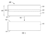
図1は、バルク結晶AlN基板140とこのバルクAlN基板140上に形成させたエピタキシャル層150とを最初に含むサブアセンブリ100を示す図である。図1はいくつかのエピタキシャル層150を示しているが、サブアセンブリはこれより多いまたは少ないエピタキシャル層を含んでよいし、一部の実施においては1層のみのエピタキシャル層を含んでもよい。AlN基板140は、第1の表面141と第2の表面142と有している。バルク結晶AlN基板は、第1と第2の表面141、142においてスライスされるインゴットとして成長させてよい。
FIG. 1 shows a
場合により、図1に示すように、エピタキシャル層150は、第1のヘテロ構造110と第2のヘテロ構造130に挟まれた1層以上の発光層120を含む。発光層120および/またはヘテロ構造110、130は、低欠陥密度でAlN上にエピタキシャル成長させることができる材料系、GaN、AlGaN、InN、InGaN、および/またはInAlGaNから形成されてよい。この例では、バルクAlN基板140の真上に第1のヘテロ構造110をエピタキシャル成長させる。エピタキシャル層150の成長は、AlN基板140の第2の表面142上でエピタキシャル成長する第1のヘテロ構造110の第1の表面101から進行する。第1のヘテロ構造110は、欠陥低減層、ひずみ管理層、および/または電流分布層を含む多層を備えてよい。次に、活性領域120を第1のヘテロ構造110の真上に実質的に成長させ、かつ、第2のヘテロ構造130を活性領域120の真上に成長させる。破線160で示すように、サブアセンブリ100の形成後、バルクAlN基板140は実質的に除去される。
In some cases, as shown in FIG. 1, the
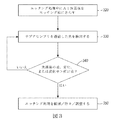
図2は、サブアセンブリからバルクAlN基板を除去する方法を示している。このサブアセンブリは、バルクAlN基板と、このバルクAlN基板上に1層以上のエピタキシャル成長層とを含む。たとえば、この1層以上のエピタキシャル層は、発光層を有する発光素子または発光層を含まないエピタキシャル層を含んでよい。 FIG. 2 illustrates a method for removing a bulk AlN substrate from a subassembly. The subassembly includes a bulk AlN substrate and one or more epitaxial growth layers on the bulk AlN substrate. For example, the one or more epitaxial layers may include a light emitting element having a light emitting layer or an epitaxial layer not including a light emitting layer.
バルクAlN基板、たとえば、基板の窒素極性(N極)面は、高温、たとえば、湿潤エッチング処理においてリン酸の沸点におけるリン酸を含むエッチング液にさらされる(220)。本明細書に記載されているLED構造において、たとえば、図1に概略的に示すように、バルクAlN基板の底面は、エッチング液にN極面を付与できる。約85%以上または約87%〜約96%の濃度範囲および160℃〜210℃の温度範囲におけるリン酸は適切な時間内でバルク単結晶AlNを溶解することができる。いくつかの構成において使用されるリン酸は、たとえば、約160℃〜約180℃の温度範囲で87%〜92%の濃度範囲を有することができる。この溶解はまた、表面の初期加水分解後にAl極面を付与するAlN基板をエッチングするために使用することもできる。 The bulk AlN substrate, eg, the nitrogen polar (N pole) surface of the substrate is exposed to an etchant containing phosphoric acid at the boiling point of phosphoric acid at a high temperature, eg, a wet etch process (220). In the LED structure described herein, for example, as schematically shown in FIG. 1, the bottom surface of the bulk AlN substrate can impart an N-polar surface to the etchant. Phosphoric acid at a concentration range of about 85% or more or about 87% to about 96% and a temperature range of 160 ° C. to 210 ° C. can dissolve the bulk single crystal AlN within a reasonable time. The phosphoric acid used in some configurations can have a concentration range of 87% to 92%, for example, at a temperature range of about 160 ° C to about 180 ° C. This dissolution can also be used to etch an AlN substrate that provides an Al polar face after initial hydrolysis of the surface.
エッチング処理中、エッチング処理パラメータ、たとえば、リン酸の濃度および/または温度が監視され得(225)リン酸の濃度および/または温度が所定の濃度および/または温度範囲内に留まるように調整され得る。エッチング処理中、AlN基板の厚さを監視することができる(230)。場合により、AlN基板の厚さは移動位置において測定され、この厚さ測定は、エッチング処理からサブアセンブリを定期的に除去し、サブアセンブリの厚さおよび/または窒化アルミニウム基板の厚さを測定し、場合によっては測定後このサブアセンブリをエッチング処理へ戻す工程を含む。他のケースにおいて、以下に説明するように、サブアセンブリおよび/またはAlN基板の厚さは原位置で測定することができる。 During the etching process, etching process parameters, eg, phosphoric acid concentration and / or temperature, can be monitored (225) and the phosphoric acid concentration and / or temperature can be adjusted to remain within a predetermined concentration and / or temperature range. . During the etching process, the thickness of the AlN substrate can be monitored (230). In some cases, the thickness of the AlN substrate is measured at the moving position, and this thickness measurement periodically removes the subassembly from the etching process and measures the thickness of the subassembly and / or the thickness of the aluminum nitride substrate. Optionally returning the subassembly to an etching process after measurement. In other cases, as described below, the thickness of the subassembly and / or AlN substrate can be measured in situ.
エッチング処理は、サブアセンブリおよび/またはAlN基板の測定厚さに基づいて必要に応じて調整することができる(240)。エッチング処理は、エッチング速度を変化させ(エッチング速度を増減させ)、エッチング処理を開始し、および/または、基板が所定の状態に入った後、たとえば、基板がサブアセンブリから実質的に除去された後、または、基板が所定の厚さ、たとえば、約50mmに達した時、または基板がサブアセンブリの領域内で実質的に除去された時、エッチング処理を停止するように、調整することができる。エッチング速度はエッチング液の濃度および/または温度を変化させることによって調整することができる。たとえば、AlNの厚さが所定の厚さに近づく(または基板の実質的な除去に近づく)につれて、エッチング速度はチャンバに水を添加することによって遅延させてエッチング液の濃度を低下させることができる。これに代えてまたはこれに加えて、エッチング速度を遅延させるためにエッチング液の温度を下げてもよい。いくつかの実施において、エッチング処理を停止することは、手動または自動の除去技術のいずれかにより、エッチング液からサブアセンブリを除去して達成することが可能である。 The etching process can be adjusted as needed based on the measured thickness of the subassembly and / or AlN substrate (240). The etch process changes the etch rate (increases or decreases the etch rate), initiates the etch process, and / or after the substrate has entered a predetermined state, for example, the substrate is substantially removed from the subassembly Later, or when the substrate reaches a predetermined thickness, eg, about 50 mm, or when the substrate is substantially removed within the region of the subassembly, it can be adjusted to stop the etching process. . The etching rate can be adjusted by changing the concentration and / or temperature of the etching solution. For example, as the thickness of AlN approaches a predetermined thickness (or approaches the substantial removal of the substrate), the etch rate can be delayed by adding water to the chamber to reduce the etchant concentration. . Alternatively or in addition, the temperature of the etchant may be lowered to delay the etch rate. In some implementations, stopping the etching process can be accomplished by removing the subassembly from the etchant, either by manual or automatic removal techniques.
サブアセンブリおよび/または窒化アルミニウム基板の厚さ測定は、機械的、電気的、化学的、および/または光学的技術を含む様々な処理によって達成可能である。たとえば、いくつかの構成において、AlN基板の厚さ測定は電磁放射を使用する光学的技術によって達成可能である。これらの技術は、電磁放射をサブアセンブリへ方向付けるソースと、回折され、反射されおよび/またはサブアセンブリによって透過される電磁放射を検出するように構成されている検出器と、を必要とする。たとえば、サブアセンブリおよび/またはAlN基板の厚さは、X線回折、偏光解析法、および/または干渉分光法などの技術を用いて測定可能である。いくつかの構成において、計測ユニットは、エッチング処理中に原位置で厚さ測定されるように配置できる。他の構成において、厚さは、エッチング処理からサブアセンブリを除去し、測定し、このサブアセンブリをエッチング処理に戻すことによって移動位置で測定される。 Measuring the thickness of the subassembly and / or aluminum nitride substrate can be accomplished by various processes including mechanical, electrical, chemical, and / or optical techniques. For example, in some configurations, AlN substrate thickness measurement can be accomplished by optical techniques using electromagnetic radiation. These techniques require a source that directs electromagnetic radiation to the subassembly and a detector that is configured to detect electromagnetic radiation that is diffracted, reflected, and / or transmitted by the subassembly. For example, the thickness of the subassembly and / or AlN substrate can be measured using techniques such as X-ray diffraction, ellipsometry, and / or interferometry. In some configurations, the metrology unit can be arranged so that the thickness is measured in situ during the etching process. In other configurations, the thickness is measured at the moving position by removing and measuring the subassembly from the etching process and returning the subassembly to the etching process.
いくつかの構成において、AlN基板の厚さ測定は、サブアセンブリを透過する光を検出する工程を含む。このような測定に使用される光の波長範囲は、バルクAlN基板によって実質的に吸収され、少なくともある程度エピタキシャル層によって透過される範囲のものである。図3の流れ図によって示すように、最初にエッチング処理が開始された時(320)、AlN基板は相対的に厚膜であり光に対して不透明である。(あれば)AlN基板を透過した光はエッチング処理中に検出される(330)。AlN基板がエッチングによって除去されると、このAlN基板は、基板を通過して光透過が可能となる位に薄膜化される。AlN基板の透過光の量、エッチング処理において以前測定した基準量に比較した場合の光透過の変化および/またはAlN基板を通過する光透過の変化率が検出でき(340)かつこれらをエッチング処理を調整するために用いてよい(350)。 In some configurations, measuring the thickness of the AlN substrate includes detecting light transmitted through the subassembly. The wavelength range of light used for such measurements is that which is substantially absorbed by the bulk AlN substrate and at least partially transmitted by the epitaxial layer. As shown by the flowchart of FIG. 3, when the etching process is first started (320), the AlN substrate is relatively thick and opaque to light. Light (if any) transmitted through the AlN substrate is detected during the etching process (330). When the AlN substrate is removed by etching, the AlN substrate is thinned to such an extent that light can pass through the substrate. The amount of light transmitted through the AlN substrate, the change in light transmission and / or the rate of change in light transmission through the AlN substrate compared to the reference amount previously measured in the etching process can be detected (340) and these can be etched. May be used to adjust (350).
AlxGa(1−x)N材料(X=0〜1)のエッチング速度は、アルミニウム含有量の関数として変化する。図4および図5のグラフは各々、エピタキシャル成長させたAlGaN層のエッチング時間とエッチング速度を、アルミニウムのモル分率の関数として、示している。各試料について、エッチングされているAlGaN層の厚さは、エッチング液化学槽から定期的に試料を取り出してX線スキャンを実行してAlGaN層のX線信号強度を求めることにより監視された。図4は、91%濃度と180℃の温度におけるリン酸(H3PO4)中でエッチングされた厚さ2.4μmのエピタキシャルAlxGa(1−x)N層のエッチング時間を示している。74%または67%のアルミニウムモル分率を有するAlGaNの層は5分以内で実質的に除去されたが、47%のアルミニウムモル分率を有するAlGaN層を除去するには30分以上もかかった。 The etching rate of Al x Ga (1-x) N material (X = 0-1) varies as a function of aluminum content. The graphs of FIGS. 4 and 5 each show the etch time and etch rate of the epitaxially grown AlGaN layer as a function of the aluminum mole fraction. For each sample, the thickness of the AlGaN layer being etched was monitored by periodically removing the sample from the etchant chemical bath and performing an X-ray scan to determine the X-ray signal intensity of the AlGaN layer. FIG. 4 shows the etch time of a 2.4 μm thick epitaxial Al x Ga (1-x) N layer etched in phosphoric acid (H 3 PO 4 ) at a 91% concentration and a temperature of 180 ° C. . AlGaN layers with an aluminum mole fraction of 74% or 67% were substantially removed within 5 minutes, but it took over 30 minutes to remove an AlGaN layer with an aluminum mole fraction of 47% .
図5は、91%濃度および180℃の温度におけるリン酸(H3PO4)中にエピタキシャル成長させたAlxGa(1−x)Nのエッチング速度をアルミニウムモル分率の関数として示すグラフである。このグラフは、アルミニウムモル分率が高くなるにつれてエッチング速度も速くなることを示している。図6は、基板の除去前(610)と基板の除去後(620)の試料サブアセンブリのX線回折測定の一例である。以下に詳細に説明するように、相対的に高いモル分率のエピタキシャル成長させたAlGaNの層は、バルクAlN基板を除去するための中間層として使用することができる。 FIG. 5 is a graph showing the etch rate of Al x Ga (1-x) N epitaxially grown in phosphoric acid (H 3 PO 4 ) at a 91% concentration and a temperature of 180 ° C. as a function of aluminum mole fraction. . This graph shows that the etching rate increases as the aluminum mole fraction increases. FIG. 6 is an example of X-ray diffraction measurement of the sample subassembly before substrate removal (610) and after substrate removal (620). As will be described in detail below, a relatively high mole fraction epitaxially grown layer of AlGaN can be used as an intermediate layer to remove the bulk AlN substrate.
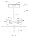
図7は、湿潤エッチングによりサブアセンブリからAlN基板を除去するために使用することができる装置を示す図である。この装置はエッチング液チャンバ710を含み、このチャンバはエッチング液を含有するとともにエッチングされているサブアセンブリを保持するように構成されている。この装置は必要に応じて計測ユニット720を含み、この計測ユニットはAlN基板の厚さおよび/またはAlN基板と1層以上のエピタキシャル層との両方を含むサブアセンブリの厚さとを示す信号を生成するように構成されている。この信号はエッチング処理中に計測ユニット720によって生成され一連の厚さ測定値を反映することが可能である。この信号はエッチング処理の1つ以上の側面を調整するためにコントロールユニット730によって使用され得る。
FIG. 7 illustrates an apparatus that can be used to remove an AlN substrate from a subassembly by wet etching. The apparatus includes an
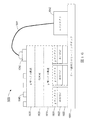
エッチング処理の調整は、エッチング処理のさまざまな側面を調整するように配置されたコントロールユニット730の1つ以上のサブユニットによって達成される。たとえば、サブユニット731、732、733は、エッチング液の温度、エッチング液の濃度、および/または試料の位置を調整することが可能である。サブアセンブリのエッチング速度は、これらの1つ以上および/または他のパラメータを変更することによって調整可能である。濃度調整サブユニット732は、チャンバ710へより多くの水分を添加することによって、またはチャンバ710内の水分を減少させることによって、例えば、沸騰時に蒸発する水分を補給しないことによって、エッチング液の濃度を維持したり変更したりするように構成することができる。温度調整サブユニット731は、エッチング液を加熱および/または冷却するヒータおよびクーラの1つまたは両方を含んでよい。エッチング液の冷却および/またはエッチング液の濃度低下はエッチング速度を遅らせる。エッチング液の温度の上昇および/または濃度の増加はエッチング速度をあるポイントまで上昇させる。しかしながら、エッチング速度はAlN基板表面の加水分解に依存することがあり得る。エッチング速度は、エッチング液の濃度が高くなりすぎ、エッチング液中の水量が表面の加水分解を発生させるには不十分な場合、抑制される。図8はバルクAlNのエッチング速度を温度の関数として示す。理解されるように、エッチング速度は約85%の濃度に対応する約160℃よりも高い温度に対しても横ばい(レベルオフ)であるように見える。この横ばいは、基板の表面を加水分解するには水分が不十分であることに起因し得る。
The adjustment of the etching process is accomplished by one or more subunits of the
いくつかの構成において、温度および/または濃度調整サブユニット731、732はエッチング液の温度および/または濃度を所定の範囲内に保つように設定される。基板の除去は、エッチング溶液を監視する工程を含む。リン酸の温度が沸点に保たれる場合、沸騰時の水分の損失はAlNの加水分解速度を減速させ、これによりエッチング速度を低下させる。リン酸の沸点は、酸の濃度に応じて変化する。たとえば、市販のリン酸は、約85%の酸の濃度を有し約158℃で沸騰する。沸騰中に水分が損失されるにつれて、酸の濃度と沸騰点は上昇する。調整されたエッチング速度の場合、エッチング液の濃度および/または温度は、所定の範囲内、たとえば、約87%〜約96%の濃度範囲および160℃〜210℃の温度範囲に保つことが可能である。相対的に一定した酸の濃度を保つために、損失した水分は、例えば、還流冷却器または自動ドリップシステムのいずれかにより補給することができる。
In some configurations, the temperature and / or
計測ユニット720は、センサ/検出器からの信号を処理するように構成されている適切な処理回路721に結合された(図7においてセンサ/検出器722として示す)1つ以上のセンサまたは検出器を含む。エッチング処理中、センサ/検出器722は、AlN基板および/またはサブアセンブリの厚さに関連するサブアセンブリおよび/またはエッチング液の特性における変化を検出する。前述したように、計測ユニット720は、厚さを示す信号を生成するために様々な技術を使用することができる。これらの技術は、エッチング処理中のAlN基板、サブアセンブリおよび/またはエッチング液の光学的、機械的、化学的、または電気的パラメータを感知する工程を含んでよい。一例として、サブアセンブリの厚さの機械的な測定は、プロフィルメータを使用して行われてもよい。この例の場合、プロフィルメータの探り針(プローブ)は計測ユニットのセンサである。サブアセンブリはエッチング処理中に数回測定される。図9はサブアセンブリのプロフィルメータの測定値の重畳したグラフを示す。厚さプロファイルIはサブアセンブリのAlN基板がエッチングされる前の起動プロファイルである。この起動プロファイル(プロファイルI)を取得した後、第1の期間でサブアセンブリをエッチング槽に入れ、次に除去し厚さプロファイルを再測定した。プロファイルAは、第1の期間においてエッチング後のアセンブリの厚さを表している。プロファイルAを取得した後、第2の期間においてサブアセンブリをエッチングした。第2の期間を経た後、プロファイルBに示すように、サブアセンブリの厚さを再測定した。連続するプロファイルI、A、Bは第1および第2の期間を経た後のエッチング処理の進行状況を示している。
The
サブアセンブリの電気的特性は厚さを示す信号を生成するために使用される。たとえば、センサは、サブアセンブリの表面または部分に電気接触するように構成されている電気コンタクトを含んでよい。電気コンタクトは、1つ以上の電気的特性処理を実施するように構成されている回路に結合される。サブアセンブリの電気的特性は、抵抗/コンダクタンス測定値、静電容量測定値、電流−電圧特性、および/または他の特性の1つ以上を含んでよい。サブアセンブリの厚さの薄膜化は、サブアセンブリの電気的特性における検出可能な変化を生成する。 The electrical properties of the subassembly are used to generate a signal indicative of thickness. For example, the sensor may include an electrical contact configured to make electrical contact with a surface or portion of the subassembly. The electrical contact is coupled to a circuit that is configured to perform one or more electrical property processing. The electrical characteristics of the subassembly may include one or more of resistance / conductance measurements, capacitance measurements, current-voltage characteristics, and / or other characteristics. Thinning the subassembly thickness produces a detectable change in the electrical properties of the subassembly.
計測ユニットはサブアセンブリおよび/またはエッチング液における化学変化を検出するように構成されている化学センサとこれらに関連する回路とを含んでよい。化学センサは、サブアセンブリの上、および/または、エッチング液槽などのエッチングチャンバ内に配置することができる。場合により、化学センサとこれらに関連する回路は、エッチング槽中のイオン濃度を測定するように構成されている。この濃度は、エッチング液に溶解される状態になるAlNの量の関数として、エッチング処理中に変化し得る。よって、化学センサによって検出されたイオン濃度は、AlN基板の厚さを示す信号を生成するために使用可能である。いくつかの構成において、これは、エッチングされている表面にてイオン濃度に対する感度を高めるためにサブアセンブリの近傍、例えば、サブアセンブリの数mm以内に化学センサを配置するために有用であり得る。 The metrology unit may include chemical sensors and associated circuitry that are configured to detect chemical changes in the subassembly and / or etchant. The chemical sensor can be placed on the subassembly and / or in an etching chamber such as an etchant bath. In some cases, the chemical sensors and their associated circuitry are configured to measure the ion concentration in the etch bath. This concentration can change during the etching process as a function of the amount of AlN that becomes dissolved in the etchant. Thus, the ion concentration detected by the chemical sensor can be used to generate a signal indicative of the thickness of the AlN substrate. In some configurations, this can be useful for placing chemical sensors near the subassembly, eg, within a few millimeters of the subassembly, to increase sensitivity to ion concentration at the surface being etched.
計測ユニットは、基板の厚さを示す信号を生成するためにサブアセンブリを透過した光を使用することができる。これらの実施において、計測ユニットは、光をサブアセンブリへ方向付けるように配置された光源と、透過した光を検出するように配置された検出器と、を含んでよい。光源は、1つ以上のランプ、LED、および/またはUV、可視光、赤外光、または広帯域光を放つレーザを含んでよい。サブアセンブリへ方向付けられた光は、AlN基板に実質的に光学的に吸収されるがサブアセンブリのエピタキシャル層には実質的に吸収されない波長範囲を含む。たとえば、バルクAlN基板とAlGaNエピタキシャル層とを含むサブアセンブリに対して、計測ユニットは、光源、例えば、約200nm〜約365nmの波長範囲で発光するLEDと同範囲で光を検出する検出器とを含んでよい。いくつかの構成において、光源は発光し得、検出器は約250nm〜約300nmの波長範囲の光を検出し得る。 The metrology unit can use the light transmitted through the subassembly to generate a signal indicative of the thickness of the substrate. In these implementations, the metrology unit may include a light source arranged to direct light to the subassembly and a detector arranged to detect the transmitted light. The light source may include one or more lamps, LEDs, and / or lasers that emit UV, visible, infrared, or broadband light. The light directed to the subassembly includes a wavelength range that is substantially optically absorbed by the AlN substrate but not substantially absorbed by the epitaxial layer of the subassembly. For example, for a subassembly that includes a bulk AlN substrate and an AlGaN epitaxial layer, the metrology unit includes a light source, for example, an LED that emits light in the wavelength range of about 200 nm to about 365 nm, and a detector that detects light in the same range. May include. In some configurations, the light source can emit light and the detector can detect light in the wavelength range of about 250 nm to about 300 nm.
場合により、光源はある波長範囲を有する光を出力するように構成され、検出器は波長範囲にわたってサブアセンブリのスペクトル応答を特徴づけるように構成されている。スペクトル応答における変化は、エッチング処理を調整するために使用可能である。 In some cases, the light source is configured to output light having a wavelength range, and the detector is configured to characterize the spectral response of the subassembly over the wavelength range. Changes in the spectral response can be used to tune the etching process.
図10は、厚さを示す信号を生成するために光を使用する装置1000を示す図である。図10の構成例において、バルクAlN基板1011とAlN基板1011上の1層以上のエピタキシャル層1012とを含むサブアセンブリ1010は、エッチング液チャンバ1020内に配置されている。熱素子1030、たとえば、ヒータおよび/またはクーラはエッチング処理中にエッチング液の温度を調整するためにチャンバ1020の中、その上、またはその周りに配置することができる。これに加えてまたはこれに代えて、装置1000は、チャンバ内のエッチング液の濃度を調整するように構成されている構造(図示せず)を含んでよい。光源、たとえば、UVLED(紫外線発光ダイオード)は光がサブアセンブリへ向けて方向付けられるように配置される。図10に示すように、光は光ファイバ1050を介してサブアセンブリ1011に向けて方向付けることが可能である。エッチング処理に先立って、光源1040からの光はバルクAlN基板1011により実質的に遮断されるが、エピタキシャル層1012により実質的に透過される。基板1011が薄膜化されるにつれて、光はサブアセンブリ1010を透過することが可能である。透過光1070は光検出器1080によって検出される。サブアセンブリ1010を透過した光1070に応答して、光検出器1080はAlN基板1011の厚さを示す出力信号1090を生成する。
FIG. 10 shows an
エッチング処理中にAlN基板の厚さを検出するために光を使用する装置1100の他の例を図11に示す。装置1100は、リン酸槽を含む石英タンク1120を備えるエッチング液チャンバを含む。AlN基板とこの上に形成した1層以上のエピタキシャル層とを含むサブアセンブリ1110は試料ホルダ1121によりタンク1120内に位置決めされ保持される。装置1100は、各々が真空に結合されている2つのポート1122、1123を含む。この例において、ポート1122、1123は閉端された真空石英管を含む。光源1140からの光は、第1のポート1122を介して第1の光ファイバ1150によって導かれ、第1のミラー1124によってサブアセンブリ1110に向けて方向付けられる。サブアセンブリ1110を透過した光は第2のポートから第2の光ファイバ1151を介して第2のミラー1125によって方向付けられる。光検出器1180はサブアセンブリ1110を透過した光を検出するように配置される。検出された光に応答して、光検出器1180は、AlN基板の厚さを示す信号1190を生成する。
Another example of an
いくつかの実施において、サブアセンブリのエピタキシャル層はLEDなどの発光素子を形成する。これらの実施において、発光素子はAlN基板の厚さを示す信号を生成する際に使用される光のための光源であってよい。図12は、AlN基板の厚さを測定するために使用される光1270を生成するためにサブアセンブリ1210のエピタキシャル層1212を使用する装置1200を示す。装置1200は、図10に示した外部光源と光ファイバが図12に示した実施では使用されていないことを除いて、いくつかの点で図10の装置と同様である。サブアセンブリ1210はエッチング液チャンバ1220内に配置されるとともにAlN基板1211上にエピタキシャル成長させる層1212を含む。エピタキシャル層1212は発光素子を形成する。装置1200は、発光素子1212と接触する電気コンタクト1232、1233と、これらの電気コンタクト1232、1233を電源1240に接続するリード1234、1235と、を含む。発光素子1212がリード1234、1235と電気コンタクト1232、1233を介して電源1240によって通電されると、発光素子1212は、基板が光1270を透過するために十分に薄膜化された時にAlN基板を透過する光1270を生成する。AlN基板1211がエッチングされると、この基板1211は増量する光1270を透過し、この光量は光検出器1280によって検出される。光検出器1280は、AlN基板の厚さを示す信号1290を生成する。
In some implementations, the epitaxial layers of the subassembly form a light emitting device such as an LED. In these implementations, the light emitting element may be a light source for light used in generating a signal indicative of the thickness of the AlN substrate. FIG. 12 shows an
図13は、たとえば、AlN基板の厚さを示す光検出器によって生成される、理想的な信号の一例を示す。最初にAlN基板はこのAlN基板に向けて透過される光を実質的に光学的に吸収している。エッチング処理が最初に開始されると、AlN基板に方向付けられた光の多くが基板によって吸収されてサブアセンブリから抜け出さない。この厚さ信号は、AlN基板の厚さがAlN層を光が透過する位に薄膜化されるまで、公称値のままである。窒化アルミニウム基板が光を透過する位に薄膜化されると、厚さ信号はAlNが基板からエッチングされればされるほど、一層増え始める。信号の変化はAlN基板の厚さがかなりの光量を透過する値に達した時、極めて速くなる。 FIG. 13 shows an example of an ideal signal generated by, for example, a photodetector indicating the thickness of the AlN substrate. Initially, the AlN substrate substantially optically absorbs light transmitted toward the AlN substrate. When the etching process is first started, much of the light directed to the AlN substrate is absorbed by the substrate and does not escape from the subassembly. This thickness signal remains at a nominal value until the thickness of the AlN substrate is thinned to such an extent that light can pass through the AlN layer. As the aluminum nitride substrate is made thin enough to transmit light, the thickness signal begins to increase as the AlN is etched from the substrate. The change of the signal becomes extremely fast when the thickness of the AlN substrate reaches a value that transmits a considerable amount of light.
場合により、計測ユニットにより生成された信号はエッチング処理を調整するために使用することができる。たとえば、コントロールユニットは急速な変化が検出されるポイントまで信号を監視してよい。その時点で、コントロールユニットはエッチング速度を変更させるように、たとえば、エッチング処理を遅延させたり停止させたりするように、動作してよい。計測ユニットにより生成された信号はエッチング処理を調整するために他の情報と組み合わせて使用される。たとえば、計測ユニットによって生成された信号に加えて、コントロールユニットは、エッチング処理期間、エッチング処理期間にわたるチャンバ内のエッチング液の濃度、および/またはエッチング処理期間にわたるエッチング液の温度などの要因を考慮に入れる。コントロールユニットは感熱ユニット、たとえば、ヒータやクーラの動作を調整し、および/またはエッチング処理の速度を変更するためにエッチング液の濃度を調整することができる。 In some cases, the signal generated by the metrology unit can be used to adjust the etching process. For example, the control unit may monitor the signal up to the point where a rapid change is detected. At that point, the control unit may operate to change the etch rate, for example, to delay or stop the etching process. The signal generated by the metrology unit is used in combination with other information to adjust the etching process. For example, in addition to the signal generated by the metrology unit, the control unit takes into account factors such as the etching process period, the concentration of the etchant in the chamber over the etch process period, and / or the temperature of the etchant over the etch process period. Put in. The control unit can adjust the concentration of the etchant to adjust the operation of a thermal unit, eg, a heater or cooler, and / or to change the speed of the etching process.
様々なタイプの発光素子は本明細書中に記載されているバルクAlN基板を除去するための処理を用いて形成されてよい。バルクAlN基板の除去や薄膜化は、約200nm〜約365nmまたは約250nm〜約320nmの波長範囲の光を放つ紫外線発光ダイオード(UVLED)と紫外線(UV)レーザダイオードに特に有用である。これらの発光素子の形成におけるバルクAlN基板の使用は、素子構造の低欠陥エピタキシャル層の成長を可能にするが、AlN基板は素子の基板側に向けた活性領域から放たれた光を実質的に吸収する。したがって、基板の除去は素子の基板側(裏面)から増加した発光を可能にする。いくつかの素子において、基板から活性層の反対側にある発光素子の上層(すなわち、素子の正面側にある層)は、素子によって生成された光の波長で光学的に吸収している状態であり得る。したがって、これは、AlN基板の除去によって実現可能となる素子によって生成された光が基板側を通過して放たれる場合に有用である。 Various types of light emitting devices may be formed using the process for removing a bulk AlN substrate described herein. Removal or thinning of the bulk AlN substrate is particularly useful for ultraviolet light emitting diodes (UVLEDs) and ultraviolet (UV) laser diodes that emit light in the wavelength range of about 200 nm to about 365 nm or about 250 nm to about 320 nm. The use of a bulk AlN substrate in the formation of these light emitting devices allows the growth of a low defect epitaxial layer of the device structure, but the AlN substrate substantially emits light emitted from the active region toward the substrate side of the device. Absorb. Therefore, the removal of the substrate enables increased light emission from the substrate side (back surface) of the element. In some devices, the upper layer of the light emitting device on the opposite side of the active layer from the substrate (ie, the layer on the front side of the device) is optically absorbing at the wavelength of the light generated by the device. possible. This is therefore useful when light generated by an element that can be realized by removal of the AlN substrate is emitted through the substrate side.
図14は、バルクAlN基板1410上に初期に成長させたUVLED1400を示す図である。エピタキシャル層の成長は、例えば、ハイドライド気相成長法(HVPE)および/またはこれらの技術の任意の組み合わせにより、有機金属気相成長法(MOCVD)を用いて、達成される。次に、バルクAlN基板1410は、矢印1411で示されるように、除去されるかまたは薄膜化することが可能である。場合により、AlN基板1410は除去されてよい。場合により、AlN基板1410は、たとえば、機械的な技術を用いて可能とされる厚さよりも薄く、約50μm以下の厚さまで薄膜化されてよい。図14に示したUVLEDヘテロ構造1400は、有機金属気相成長法により以下を含むように成長可能である:
n側のAlxGa1−xN遷移領域1420と、
nドープAl0.74Ga0.26Nのnコンタクト層1430と、
n側のAl0.74Ga0.26Nの分離した閉じ込めヘテロ構造(SCH)1440と、
例えば、中心周波数λ=250nmで発光するように設計された、多重量子井戸(MQW)発光層1450と、
電子遮断層1460と、
p側AlGaNのSCH1470、p型ドープAlGaN遷移領域1480と、
pドープGaNコンタクト層1490。
FIG. 14 is a diagram illustrating a
an n-side Al x Ga 1-x
an n-
n-side Al 0.74 Ga 0.26 N isolated confinement heterostructure (SCH) 1440;
For example, a multiple quantum well (MQW) light emitting
An
p-doped
n側のAlxGa1−xNの遷移領域1420は、AlN基板1410上に形成されたエピタキシャル成長の初期表面1405を含む。いくつかの構成において、n側遷移領域1420は、約0.90に等しいxから約0.80に等しいxまでの範囲の平均Al(アルミニウム)組成を有する一連の短周期超格子である。いくつかの構成において、遷移領域1420は、xが約100%から約74%までの範囲の線形グレード合金であってよい。nコンタクト層1430は、nコンタクト1435のためのコンタクト層であり、たとえば、約1.9μm厚さであってよい。量子井戸(MQW)発光層1450は3対の6nm厚さのAl0.68Ga0.32Nバリアと、2nm厚さのAl0.65Ga0.35Nウェルを含むことができる。電子遮断層(EBL)1460は、約83%のアルミニウムと約20nmの厚さであってよい。p−SCH1470は約0.3から約0.74までの範囲のアルミニウム組成xを有することができる。p遷移層1480は超格子であるかまたは約0.3から約0.74までの範囲xを有する合金であってよい。pコンタクト層1490は、GaNを含みかつp型金属コンタクト1495のためのコンタクト層である。記載した構造は一例にすぎない。層数、層の組成、実際のヘテロ構造の設計、および/または成長手順は大きく異なる。具体的には、これらの層はAlGaNに代えてInGaNまたはInAlGaNを形成するためにインジウムを含むことができる。
The n-side Al x Ga 1-x
LEDをバルクAlN基板上に最初に成長させて、次にこの基板を除去するかまたは薄膜化する。この処理は、たとえば、約108cm−3または107cm−3などの約1010cm−3〜約103cm−3の範囲において相対的に低くなるようにAlGaN遷移層のエピタキシャル成長の初期表面において欠陥密度を生成する。このように、素子はAlN基板に整合する実質的な格子によってもたらされる高品質のエピタキシャル成長を保持するが、この素子の基板側を通過する実質的な光透過を可能とすることもできる。 The LED is first grown on a bulk AlN substrate, which is then removed or thinned. This treatment is for example early in the epitaxial growth of the AlGaN transition layer to be relatively low in the range of about 10 10 cm −3 to about 10 3 cm −3 , such as about 10 8 cm −3 or 10 7 cm −3. Generate defect density at the surface. In this way, the device retains the high quality epitaxial growth provided by the substantial lattice matching the AlN substrate, but may also allow substantial light transmission through the substrate side of the device.
たとえば、バルクAlN基板上にエピタキシャル成長させる約70%〜80%未満のAlモル分率を有するAlGaNのn遷移層は基板にぴったり格子整合すると思われる。この場合、AlGaNのn遷移層は低欠陥密度を有するバルク結晶AlNの格子定数にぴったり整合するように不整合な状態である。AlN基板が除去されると、n遷移層の格子は緩むが、低欠陥密度は保持される。 For example, an AlGaN n-transition layer having an Al mole fraction of about 70% to less than 80% grown epitaxially on a bulk AlN substrate appears to be closely lattice matched to the substrate. In this case, the AlGaN n-transition layer is in a mismatched state so as to closely match the lattice constant of the bulk crystal AlN having a low defect density. When the AlN substrate is removed, the lattice of the n-transition layer relaxes, but the low defect density is retained.
図15は、図14のLED1400にいくつかの点で類似しているLEDを示す。図15において参照符号で識別される要素は、図14におけるこれらの片われ(カウンターパート)に類似している。LED1500は、このLED1500がエッチング前にAlN基板1410とAlGaN遷移層1420との間で成長可能なエッチング低減層1510(エッチング停止層ともいう)を含む点で、図14のLED1400とは異なる。この例において、エッチング低減層1510は初期のエピタキシャル表面1505を含む。エッチング低減層1510は、AlN基板をエッチングするために使用されるエッチング液に不浸透性であるかまたはエッチング液中のエッチング低減層のエッチング速度は、AlN1410のエッチング速度より低速であり得る。エッチング低減層1510は、相対的に薄層のGaN層であるかまたは約70%〜約80%の範囲のアルミニウム含有量(Alモル分率)を有するAlGaN層であるかおよび/または、たとえば、エッチング低減能力を付与する他の適切な材料を含んでよい。
FIG. 15 shows an LED that is similar in some respects to
約50μm未満の厚さを有する基板残部を残すための完全な除去または化学的なエッチングのいずれかによる基板の除去によってこの後の処理のために素子の裏面へのアクセスが可能となる。基板が除去された後は素子の裏面にある量の表面粗さやテクスチャリングが存在している。場合により、テクスチャリングは、この基板除去処理によって素子の裏面へ付与されてよい。この基板除去処理は、この基板除去処理中にこの素子の裏面のテクスチャリングを付与するように構成されてよい。化学エッチングから得られた表面粗さはエッチング槽温度、酸濃度、エッチング速度、および/またはウェハ裏面磨きなどの処理パラメータに依存する。適切な処理パラメータは、所望される表面粗さ特性を生成するために選択され得る。この場合、素子の裏面は、たとえば、イオンビームまたは化学処理によって、基板除去後にテクスチャリングすることができる。テクスチャリングは光抽出を向上させることができる。この場合、裏面のテクスチャリングを行わずに、実質的な発光量を全内部反射によってヘテロ構造に閉じ込めることができる。裏面のテクスチャリングは放たれた光を散乱させ、全内部反射を妨げ、かつ光抽出効率を向上させる。 Removal of the substrate, either by complete removal to leave the remainder of the substrate having a thickness of less than about 50 μm or by chemical etching, allows access to the backside of the device for subsequent processing. After the substrate is removed, there is some amount of surface roughness and texturing on the backside of the device. In some cases, texturing may be applied to the backside of the device by this substrate removal process. The substrate removal process may be configured to provide texturing of the back surface of the element during the substrate removal process. The surface roughness obtained from chemical etching depends on processing parameters such as etch bath temperature, acid concentration, etch rate, and / or wafer backside polishing. Appropriate processing parameters can be selected to produce the desired surface roughness characteristics. In this case, the back surface of the element can be textured after removal of the substrate, for example by ion beam or chemical treatment. Texturing can improve light extraction. In this case, a substantial amount of light emission can be confined in the heterostructure by total internal reflection without texturing the back surface. Backside texturing scatters emitted light, prevents total internal reflection, and improves light extraction efficiency.
表面テクスチャリングは様々な湿式または乾式の処理技術によってパターン化することができる。たとえば、表面は水素化カリウム(KOH)溶液に浸漬することによりテクスチャリングすることができる。プラズマ処理技術は粗面処理するために使用することができる。たとえば、LED1400、1500の初期のエピタキシャル表面1405、1505はテクスチャリングされた表面であってよい。
Surface texturing can be patterned by various wet or dry processing techniques. For example, the surface can be textured by dipping in a potassium hydride (KOH) solution. Plasma processing techniques can be used to roughen the surface. For example, the
裏面のテクスチャリングは放たれた光がより短い波長でTM方向(平面に垂直な方向)において偏光状態が強くなるので、短波長のUVLEDにおいて特に重要である。これによって、光の大部分は裏面へ向けてよりもむしろ、素子の端部へ向けて伝搬しながら発光される。基板が除去されて、特性は裏面へ向けてかつ裏面を通過して放たれた光を再方向付けするようにパターン化することができる。 Backside texturing is particularly important for short wavelength UVLEDs because the emitted light has a stronger polarization state in the TM direction (direction perpendicular to the plane) at shorter wavelengths. As a result, most of the light is emitted while propagating toward the end of the device rather than toward the back surface. With the substrate removed, the characteristics can be patterned to redirect the light emitted toward and through the back surface.
基板の除去によって垂直方向の電気的注入LEDアーキテクチャも可能になる。図16はこのような構造1600を示す。このLEDは初期エピタキシャル表面1631を含むn型のヘテロ構造1630を含む。n型のヘテロ構造の初期のエピタキシャル表面からはじめて発光層1620とp型ヘテロ構造1610を連続的にエピタキシャル成長させて、LED1600をバルク結晶AlN基板(図16に図示せず)上に成長させた。エピタキシャル層1610〜1630を形成した後、バルクAlN基板が除去された。
Removal of the substrate also allows for a vertical electrical injection LED architecture. FIG. 16 shows such a
垂直方向注入LED1600のpコンタクト1605は、ヒートシンクチップ1601のパッド1602へ半田付け1603される。電極1640は、1つ以上のリード1641とnコンタクト1642を介してヒートシンクチップ1601に電気的に結合される。素子の動作中、電流は、pコンタクト1605、p側(p型ヘテロ構造1610)、発光層1620、およびn側(n型ヘテロ構造1630)を介して、外部電源(図示せず)から注入されるとともに素子1600の裏面に形成された電極1640にて集合される。電気的絶縁性のAlN基板を除去することによって裏面コンタクト1640を形成するためのn型ヘテロ構造層1630へのアクセスが可能となる。
The p-
図16に示した垂直方向注入構造1600は、n型ヘテロ構造1630を形成する材料、たとえば、nドープAlGaNが大きく抵抗性を示す場合、特に有利になり得る。この状況において、AlN基板を除去しない場合、電流は、素子1600のpコンタクト1605と同じ側で、発光領域1620に並んだ領域において、集合される(たとえば、図14と図15のLED1400、1500、1600の構造を参照されたい)。より高い光出力パワーを得るために、発光層1620の面積は相対的に大きくなるように作られる。発光層の中心に注入される電流は、素子の周囲のnコンタクトに達する前に抵抗性のあるnドープ層内でより長い横方向の距離を移動する必要があると思われる。この横方向の距離に沿った電流経路は大きな電圧降下を生成しかつ不均一な電流注入を生じさせることができる。AlN基板の除去は、コンタクトを素子の裏面に形成することを可能にし、これによりpコンタクト1602と電流収集電極1640との間により直接的な電流経路とより低い電圧降下をもたらす。
The
レーザダイオード(LD)もまた、AlN基板の除去や薄膜化を有利とすることができる。図17は関連する光学モードプロファイル(破線で示す)とともに典型的なレーザーダイオード設計(実線で示す)のエネルギバリア図を示す。モードの中心周波数は、約250nmの波長に対応する。この設計において、光学モードと量子井戸1730の間のオーバーラップは、Γ=8.26%で表される。LDは、nコンタクト1710、n‐SCH1720、多重量子井戸1730、p‐SCH1740、およびpコンタクト1760を含む。
Laser diodes (LDs) can also benefit from the removal and thinning of AlN substrates. FIG. 17 shows an energy barrier diagram of a typical laser diode design (shown as a solid line) with an associated optical mode profile (shown as a dashed line). The center frequency of the mode corresponds to a wavelength of about 250 nm. In this design, the overlap between the optical mode and the
AlN基板上に作られた一般的なUVレーザダイオードにおいて、何らかの電界がAlN基板に浸透している場合、このAlN基板がレーザ処理波長において高く光吸収するので、実質的なモーダル損失が生じる。光吸収基板は、導波管材料の損失を助長し、これによりレーザ処理を達成するために必要とされる利得を増加させる。基板側のクラッド層は、活性領域内に光学モードをしっかりと閉じ込めるために十分に厚くする必要がある。しかしながら、厚膜のnクラッド層は素子の抵抗性を助長する。AlN基板を除去または薄膜化することは、モーダル損失を低減し、設計上のフレキシビリティを高める。AlN基板の除去および/または薄膜化はまた、LEDのケースにおいて説明した利益に類似した利益を提供する垂直方向の注入LD構造を可能にする。 In a general UV laser diode fabricated on an AlN substrate, if any electric field penetrates the AlN substrate, this AlN substrate absorbs high at the laser processing wavelength, resulting in substantial modal loss. The light absorbing substrate facilitates the loss of the waveguide material, thereby increasing the gain required to achieve laser processing. The cladding layer on the substrate side needs to be thick enough to tightly confine the optical mode in the active region. However, the thick n-cladding layer promotes device resistance. Removing or thinning the AlN substrate reduces modal loss and increases design flexibility. The removal and / or thinning of the AlN substrate also allows for a vertical implanted LD structure that offers benefits similar to those described in the LED case.
基板の除去および/または薄膜化は、裏面全体を横切ってというよりむしろ裏面のいくつかの部分においてのみ達成され得る。基板は化学エッチング液から保護することができ、選択領域における開口は、これらの領域のみをエッチングするためだけに形成される。たとえば、開口は発光層の真下の領域においてのみ形成され、これによりバルク基板の部分はエッチング処理後に残留し、これ以降の処理のために使用可能である。 Substrate removal and / or thinning can be accomplished only in some parts of the backside rather than across the entire backside. The substrate can be protected from chemical etchants, and the openings in selected areas are formed only to etch only those areas. For example, the opening is formed only in the region directly under the light emitting layer, so that a portion of the bulk substrate remains after the etching process and can be used for further processing.
いくつかの実施において、本明細書において「テンプレート/基板」と総称されるエピタキシャル成長させたAlNまたはAlGaNテンプレートおよび/または基板は、スタンドアロン型コンポーネントとして製造することができる。これらのテンプレート/基板は、たとえば、ピースパーツとして売られ、その後、LEDやレーザーダイオードなどの光電子デバイスとヘテロ接合トランジスタや増幅器などの電子素子とを含む数多くの種類の素子を形成するために使用することができる。エピタキシャルテンプレートは、バルク結晶AlN基板上にエピタキシャルAlNまたはAlGaNを成長させ、次にこのAlN基板を除去または薄膜化することによって形成することができる。この技術は、AlN、AlGaN、InN、InGaN、および/またはInAlGaNなどの窒化物系材料の高品質で光学的に透明なエピタキシャル成長させたテンプレート/基板を生成することができ、これ以降の処理ステップにおけるエピタキシャル成長のためのベースとして使用することができる。エピタキシャルテンプレート/基板は、相対的に高い成長率、たとえば、時間あたり約1μm以上で成長させて約30μm〜約400μmの層を生成することができる。エピタキシャル成長させたテンプレート/基板は、有機金属気相成長法(MOCVD)、ハイドライド気相成長法(HVPE)、および/または、これらの技術の任意の組み合わせにより、形成してよい。高品質で光学的に透明なテンプレート/基板は、前述した理由からUVオプトエレクトロニクスデバイスに有用であり得る。最も一般的な配向はc平面のAlNであるが、m平面、a平面などの他の結晶配向や半極性配向も、エピタキシャル成長の開始前にAlNバルク基板を所望の配向において切断することによって得ることができる。 In some implementations, the epitaxially grown AlN or AlGaN template and / or substrate, collectively referred to herein as “template / substrate”, can be fabricated as a stand-alone component. These templates / substrates are sold, for example, as piece parts and then used to form many types of elements including optoelectronic devices such as LEDs and laser diodes and electronic elements such as heterojunction transistors and amplifiers. be able to. An epitaxial template can be formed by growing epitaxial AlN or AlGaN on a bulk crystal AlN substrate and then removing or thinning the AlN substrate. This technique can produce high quality, optically transparent and epitaxially grown templates / substrates of nitride based materials such as AlN, AlGaN, InN, InGaN, and / or InAlGaN, in subsequent processing steps. It can be used as a base for epitaxial growth. The epitaxial template / substrate can be grown at a relatively high growth rate, eg, about 1 μm or more per hour, to produce a layer of about 30 μm to about 400 μm. The epitaxially grown template / substrate may be formed by metal organic chemical vapor deposition (MOCVD), hydride vapor deposition (HVPE), and / or any combination of these techniques. High quality optically transparent templates / substrates can be useful for UV optoelectronic devices for the reasons described above. The most common orientation is c-plane AlN, but other crystal and semipolar orientations such as m-plane and a-plane can be obtained by cutting the AlN bulk substrate in the desired orientation before the start of epitaxial growth. Can do.
図18および図19は、スタンドアロン型のエピタキシャル成長させたテンプレート/基板を形成する処理(図19)と、これにより得られる構造(図18)と、を示す。たとえば、エピタキシャルAlN、AlGaN、InN、InGaN、および/またはInAlGaNを含むエピタキシャル層をバルク結晶AlN基板上に成長させる(1910)。得られた構造1810を図18に示す。バルクAlN基板は、本明細書において前述した処理によって除去または薄膜化されて(1920)、スタンドアロン型のエピタキシャルテンプレート/基板1820を残す。
18 and 19 illustrate the process of forming a stand-alone epitaxially grown template / substrate (FIG. 19) and the resulting structure (FIG. 18). For example, an epitaxial layer comprising epitaxial AlN, AlGaN, InN, InGaN, and / or InAlGaN is grown on a bulk crystal AlN substrate (1910). The resulting
いくつかの実施において、構造、たとえば、エピタキシャルテンプレート/基板、オプトエレクトロニクスデバイス、または他の構造またはヘテロ構造は、AlN、シリコン、サファイア、またはSiC(炭化ケイ素)などの様々な基板上に成長させた中間層上に成長させることができる。これらは中間層をエッチングすることによって基板から分離させて、これにより基板から構造を分離させることができる。図21は、中間層をエッチングすることによりその基板からスタンドアロン型のエピタキシャル成長させたヘテロ構造を形成する処理を示す。図20は、この構造の初期と最後の状態を示す。中間層2020は基板2010上にエピタキシャル成長させる(2110)。構造2030を界面層2020に成長させる(2120)。界面層2020は横方向にエッチングされ(2130)、基板2010から構造2030を分離させる。
In some implementations, structures such as epitaxial templates / substrates, optoelectronic devices, or other structures or heterostructures were grown on various substrates such as AlN, silicon, sapphire, or SiC (silicon carbide). It can be grown on an intermediate layer. These can be separated from the substrate by etching the intermediate layer, thereby separating the structure from the substrate. FIG. 21 illustrates a process for forming a stand-alone epitaxially grown heterostructure from its substrate by etching the intermediate layer. FIG. 20 shows the initial and final states of this structure. The
Claims (5)
前記バルク窒化アルミニウム基板の厚さを示す信号を生成するように構成されている計測ユニットと、
を含む装置であって、
前記バルク窒化アルミニウム基板は、前記バルク窒化アルミニウム基板の上に成長させた1層以上のエピタキシャル層を含むサブアセンブリの基板であり、
前記計測ユニットは、
前記バルク窒化アルミニウム基板によって吸収されるが前記1層以上のエピタキシャル層によって吸収されない波長の光を生成するように構成されている光源と、
前記サブアセンブリを透過した光を検出するように配置されている検出器と、
を含み、
前記検出器は、前記検出された光の波長範囲にわたって前記サブアセンブリのスペクトル応答を特徴づけるように構成されている、
装置。 A chamber configured to expose the bulk aluminum nitride substrate to an etchant during the etching process;
A measurement unit configured to generate a signal indicative of a thickness of the bulk aluminum nitride substrate;
A device comprising:
The bulk aluminum nitride substrate is a substrate of a subassembly including one or more epitaxial layers grown on the bulk aluminum nitride substrate;
The measurement unit is
A light source configured to generate light of a wavelength that is absorbed by the bulk aluminum nitride substrate but not absorbed by the one or more epitaxial layers;
A detector arranged to detect light transmitted through the subassembly;
Including
The detector is configured to characterize a spectral response of the subassembly over a range of wavelengths of the detected light;
apparatus.
前記計測ユニットは、前記電気コンタクトを介して前記サブアセンブリの1つ以上の電気的特性を測定するように構成されている、
請求項1に記載の装置。 The measurement unit includes an electrical contact configured to be in electrical contact with the subassembly;
The measurement unit is configured to measure one or more electrical characteristics of the subassembly via the electrical contacts;
The apparatus of claim 1.
前記計測ユニットは、前記イオン濃度に基づいて前記信号を生成するように構成されている、
請求項1に記載の装置。 The metrology unit includes a chemical sensor configured to sense an ion concentration in the chamber in the vicinity of the subassembly;
The measurement unit is configured to generate the signal based on the ion concentration;
The apparatus of claim 1.
請求項1に記載の装置。 The signal is an analog signal indicating the thickness of the bulk aluminum nitride substrate.
The apparatus of claim 1.
Applications Claiming Priority (2)
| Application Number | Priority Date | Filing Date | Title |
|---|---|---|---|
| US13/217,821 | 2011-08-25 | ||
| US13/217,821 US8908161B2 (en) | 2011-08-25 | 2011-08-25 | Removing aluminum nitride sections |
Publications (3)
| Publication Number | Publication Date |
|---|---|
| JP2013046063A JP2013046063A (en) | 2013-03-04 |
| JP2013046063A5 JP2013046063A5 (en) | 2015-09-17 |
| JP5833988B2 true JP5833988B2 (en) | 2015-12-16 |
Family
ID=46704547
Family Applications (1)
| Application Number | Title | Priority Date | Filing Date |
|---|---|---|---|
| JP2012171055A Active JP5833988B2 (en) | 2011-08-25 | 2012-08-01 | Removal of aluminum nitride part |
Country Status (3)
| Country | Link |
|---|---|
| US (1) | US8908161B2 (en) |
| EP (1) | EP2562800A3 (en) |
| JP (1) | JP5833988B2 (en) |
Families Citing this family (6)
| Publication number | Priority date | Publication date | Assignee | Title |
|---|---|---|---|---|
| JP6248359B2 (en) * | 2013-12-20 | 2017-12-20 | 住友電工デバイス・イノベーション株式会社 | Semiconductor layer surface treatment method |
| JP6426359B2 (en) * | 2014-03-24 | 2018-11-21 | 株式会社東芝 | Semiconductor light emitting device and method of manufacturing the same |
| US10249786B2 (en) * | 2016-11-29 | 2019-04-02 | Palo Alto Research Center Incorporated | Thin film and substrate-removed group III-nitride based devices and method |
| US10468297B1 (en) * | 2018-04-27 | 2019-11-05 | Taiwan Semiconductor Manufacturing Co., Ltd. | Metal-based etch-stop layer |
| CN114041205A (en) * | 2019-03-19 | 2022-02-11 | 动量光学公司 | Thermally-guided chemical etching of substrates and real-time monitoring thereof |
| JP2021131324A (en) * | 2020-02-20 | 2021-09-09 | キオクシア株式会社 | Thin film analyzer and method for analyzing thin film |
Family Cites Families (19)
| Publication number | Priority date | Publication date | Assignee | Title |
|---|---|---|---|---|
| US5392124A (en) | 1993-12-17 | 1995-02-21 | International Business Machines Corporation | Method and apparatus for real-time, in-situ endpoint detection and closed loop etch process control |
| TW312079B (en) * | 1994-06-06 | 1997-08-01 | Ibm | |
| US5739945A (en) | 1995-09-29 | 1998-04-14 | Tayebati; Parviz | Electrically tunable optical filter utilizing a deformable multi-layer mirror |
| US5754294A (en) * | 1996-05-03 | 1998-05-19 | Virginia Semiconductor, Inc. | Optical micrometer for measuring thickness of transparent wafers |
| FR2765347B1 (en) | 1997-06-26 | 1999-09-24 | Alsthom Cge Alcatel | SEMICONDUCTOR BRAGG REFLECTOR AND MANUFACTURING METHOD |
| US5969805A (en) * | 1997-11-04 | 1999-10-19 | Micron Technology, Inc. | Method and apparatus employing external light source for endpoint detection |
| US6081334A (en) * | 1998-04-17 | 2000-06-27 | Applied Materials, Inc | Endpoint detection for semiconductor processes |
| US6390019B1 (en) * | 1998-06-11 | 2002-05-21 | Applied Materials, Inc. | Chamber having improved process monitoring window |
| US6750152B1 (en) * | 1999-10-01 | 2004-06-15 | Delphi Technologies, Inc. | Method and apparatus for electrically testing and characterizing formation of microelectric features |
| US6635573B2 (en) * | 2001-10-29 | 2003-10-21 | Applied Materials, Inc | Method of detecting an endpoint during etching of a material within a recess |
| US8257546B2 (en) * | 2003-04-11 | 2012-09-04 | Applied Materials, Inc. | Method and system for monitoring an etch process |
| JP2005150675A (en) | 2003-11-18 | 2005-06-09 | Itswell Co Ltd | Semiconductor light-emitting diode and its manufacturing method |
| AU2003300005A1 (en) * | 2003-12-19 | 2005-08-03 | International Business Machines Corporation | Differential critical dimension and overlay metrology apparatus and measurement method |
| JP4622720B2 (en) | 2004-07-21 | 2011-02-02 | 日亜化学工業株式会社 | Method for manufacturing nitride semiconductor wafer or nitride semiconductor device |
| US20060285120A1 (en) * | 2005-02-25 | 2006-12-21 | Verity Instruments, Inc. | Method for monitoring film thickness using heterodyne reflectometry and grating interferometry |
| US8158526B2 (en) * | 2006-10-30 | 2012-04-17 | Applied Materials, Inc. | Endpoint detection for photomask etching |
| CN101918624A (en) | 2008-01-16 | 2010-12-15 | 国立大学法人东京农工大学 | Process for producing laminate comprising Al-based group III nitride single crystal layer, laminate produced by the process, process for producing Al-based group III nitride single crystal substrate using the laminate, and aluminum nitride single cry |
| US7902047B2 (en) | 2008-07-18 | 2011-03-08 | The United States Of America As Represented By The United States Department Of Energy | Dual chamber system providing simultaneous etch and deposition on opposing substrate sides for growing low defect density epitaxial layers |
| EP2253988A1 (en) * | 2008-09-19 | 2010-11-24 | Christie Digital Systems USA, Inc. | A light integrator for more than one lamp |
-
2011
- 2011-08-25 US US13/217,821 patent/US8908161B2/en active Active
-
2012
- 2012-08-01 JP JP2012171055A patent/JP5833988B2/en active Active
- 2012-08-22 EP EP12181406.5A patent/EP2562800A3/en not_active Withdrawn
Also Published As
| Publication number | Publication date |
|---|---|
| US8908161B2 (en) | 2014-12-09 |
| US20130052758A1 (en) | 2013-02-28 |
| EP2562800A2 (en) | 2013-02-27 |
| JP2013046063A (en) | 2013-03-04 |
| EP2562800A3 (en) | 2013-11-13 |
Similar Documents
| Publication | Publication Date | Title |
|---|---|---|
| JP5833988B2 (en) | Removal of aluminum nitride part | |
| US6593595B2 (en) | Semiconductor light-emitting device and method for producing same | |
| US7566579B2 (en) | Method of fabricating semiconductor devices with a multi-role facilitation layer | |
| JP6069617B2 (en) | Device from which aluminum nitride is removed | |
| JP6676578B2 (en) | Manufacturing method of semiconductor chip | |
| US6709881B2 (en) | Method for manufacturing semiconductor and method for manufacturing semiconductor device | |
| Tsujimura et al. | Characteristics of polarized electroluminescence from m-plane InGaN-based light emitting diodes | |
| JP2005322944A (en) | Methods of evaluating and manufacturing gallium nitride based semiconductor light-emitting element | |
| KR20220031723A (en) | Power Photodiode Structures, Manufacturing Methods, and Methods of Use | |
| US8306083B2 (en) | High performance ZnO-based laser diodes | |
| JP6903210B2 (en) | Semiconductor light emitting device and its manufacturing method | |
| US20080181267A1 (en) | Optical device and method for manufacturing the same | |
| JP4680015B2 (en) | Nitride semiconductor laser device and manufacturing method thereof | |
| JP2007329487A (en) | Laser element, and optical recording reproducing device | |
| Zeng et al. | Room-temperature continuous-wave operation of InGaN-based blue-violet laser diodes with a lifetime of 15.6 hours | |
| US20150200521A1 (en) | Nitride semiconductor light emitting element | |
| Koscica et al. | Impact of Pocket Geometry on Quantum Dot Lasers Grown on Silicon Wafers | |
| Li-Qun et al. | Continuous-wave operation of GaN based multi-quantum-well laser diode at room temperature | |
| Ni et al. | Nondestructive Measurement for Front Facet Temperature of Semiconductor Lasers | |
| JP2022153164A (en) | optical device | |
| KR101076723B1 (en) | An apparatus for control annealing of semiconductor light emitting device and a method thereof | |
| Kneissl et al. | Material characterization for III-nitride-based light emitters | |
| JP4935591B2 (en) | Method for fabricating group III nitride semiconductor optical device and method for measuring photoluminescence spectrum | |
| JP5685035B2 (en) | Manufacturing method of semiconductor light emitting device | |
| Kauer et al. | InGaN laser diodes by molecular beam epitaxy |
Legal Events
| Date | Code | Title | Description |
|---|---|---|---|
| RD04 | Notification of resignation of power of attorney |
Free format text: JAPANESE INTERMEDIATE CODE: A7424 Effective date: 20131209 |
|
| A521 | Request for written amendment filed |
Free format text: JAPANESE INTERMEDIATE CODE: A523 Effective date: 20150731 |
|
| A621 | Written request for application examination |
Free format text: JAPANESE INTERMEDIATE CODE: A621 Effective date: 20150731 |
|
| A871 | Explanation of circumstances concerning accelerated examination |
Free format text: JAPANESE INTERMEDIATE CODE: A871 Effective date: 20150731 |
|
| TRDD | Decision of grant or rejection written | ||
| A975 | Report on accelerated examination |
Free format text: JAPANESE INTERMEDIATE CODE: A971005 Effective date: 20150930 |
|
| A01 | Written decision to grant a patent or to grant a registration (utility model) |
Free format text: JAPANESE INTERMEDIATE CODE: A01 Effective date: 20151006 |
|
| A61 | First payment of annual fees (during grant procedure) |
Free format text: JAPANESE INTERMEDIATE CODE: A61 Effective date: 20151030 |
|
| R150 | Certificate of patent or registration of utility model |
Ref document number: 5833988 Country of ref document: JP Free format text: JAPANESE INTERMEDIATE CODE: R150 |
|
| R250 | Receipt of annual fees |
Free format text: JAPANESE INTERMEDIATE CODE: R250 |
|
| R250 | Receipt of annual fees |
Free format text: JAPANESE INTERMEDIATE CODE: R250 |
|
| R250 | Receipt of annual fees |
Free format text: JAPANESE INTERMEDIATE CODE: R250 |
|
| R250 | Receipt of annual fees |
Free format text: JAPANESE INTERMEDIATE CODE: R250 |
|
| R250 | Receipt of annual fees |
Free format text: JAPANESE INTERMEDIATE CODE: R250 |
|
| R250 | Receipt of annual fees |
Free format text: JAPANESE INTERMEDIATE CODE: R250 |