JP5824135B2 - Semiconductor device - Google Patents
Semiconductor device Download PDFInfo
- Publication number
- JP5824135B2 JP5824135B2 JP2014262313A JP2014262313A JP5824135B2 JP 5824135 B2 JP5824135 B2 JP 5824135B2 JP 2014262313 A JP2014262313 A JP 2014262313A JP 2014262313 A JP2014262313 A JP 2014262313A JP 5824135 B2 JP5824135 B2 JP 5824135B2
- Authority
- JP
- Japan
- Prior art keywords
- semiconductor chip
- source
- mosfet
- lead
- junction fet
- Prior art date
- Legal status (The legal status is an assumption and is not a legal conclusion. Google has not performed a legal analysis and makes no representation as to the accuracy of the status listed.)
- Active
Links
Images


Description
本発明は、半導体装置に関し、特に、例えば、エアコンのインバータ、コンピュータ電源のDC/DCコンバータ、ハイブリッド自動車や電気自動車のインバータモジュールなどに使用されるパワー半導体装置に適用して有効な技術に関する。 The present invention relates to a semiconductor device, and more particularly, to a technology effective when applied to a power semiconductor device used in, for example, an inverter of an air conditioner, a DC / DC converter of a computer power supply, an inverter module of a hybrid vehicle or an electric vehicle.
特表2000−506313号公報(特許文献1)には、低オン抵抗と高耐圧を両立させたスイッチング素子を提供する技術が記載されている。具体的に、特許文献1には、シリコンカーバイド(SiC)を材料とする接合FET(Junction Field Effect Transistor)と、シリコン(Si)を材料とするMOSFET(Metal Oxide Semiconductor Field Effect Transistor)をカスコード接続する構成が記載されている。
Japanese Translation of PCT International Publication No. 2000-506313 (Patent Document 1) describes a technique for providing a switching element that achieves both low on-resistance and high breakdown voltage. Specifically, in
特開2008−198735号公報(特許文献2)には、低オン電圧で高耐圧の素子を提供するために、SiCを材料とするFETと、Siを材料とするダイオードとを直列接続する構成が記載されている。 Japanese Laid-Open Patent Publication No. 2008-198735 (Patent Document 2) has a configuration in which an FET made of SiC and a diode made of Si are connected in series in order to provide an element having a low on-voltage and a high withstand voltage. Have been described.
特開2002−208673号公報(特許文献3)には、パワーモジュールの面積を削減するために、スイッチング素子と、ダイオードとを平板接続端子を挟んで積層する構造が記載されている。 Japanese Patent Laid-Open No. 2002-208673 (Patent Document 3) describes a structure in which a switching element and a diode are stacked with a flat plate connection terminal interposed therebetween in order to reduce the area of a power module.
特開2010−206100号公報(特許文献4)には、SiCを材料とするノーマリオフ型の接合FETのしきい値電圧を高くすることにより、誤点孤を防ぐ技術が記載されている。具体的には、SiC基板上に、接合FETとMOSFETとを配置し、接合FETのゲート電極に、MOSFETをダイオード接続するとしている。 Japanese Patent Laying-Open No. 2010-206100 (Patent Document 4) describes a technique for preventing false spot-off by increasing the threshold voltage of a normally-off junction FET made of SiC. Specifically, the junction FET and the MOSFET are arranged on the SiC substrate, and the MOSFET is diode-connected to the gate electrode of the junction FET.
耐圧の向上とオン抵抗の低減の両立を図るスイッチング素子として、カスコード接続方式を使用したスイッチング素子がある。カスコード接続方式を使用したスイッチング素子は、例えば、シリコン(Si)よりもバンドギャップの大きな材料を使用したノーマリオン型の接合FET(Junction Field Effect Transistor)と、シリコン(Si)を使用したノーマリオフ型のMOSFET(Metal Oxide Semiconductor Field Effect Transistor)とを直列接続した構成をしている。このカスコード接続方式のスイッチング素子によれば、絶縁耐圧の大きな接合FETにより耐圧を確保できるとともに、ノーマリオン型の接合FETによるオン抵抗の低減と、低耐圧なMOSFETによるオン抵抗の低減により、耐圧の向上とオン抵抗の低減を両立させたスイッチング素子を得ることができる。 There is a switching element that uses a cascode connection method as a switching element that achieves both improvement in breakdown voltage and reduction in on-resistance. Switching elements using the cascode connection method are, for example, normally-on junction field effect transistors (FETs) that use a material with a larger band gap than silicon (Si), and normally-off types that use silicon (Si). A MOSFET (Metal Oxide Semiconductor Field Effect Transistor) is connected in series. According to this cascode connection type switching element, the withstand voltage can be secured by a junction FET having a large withstand voltage, and the on-resistance is reduced by a normally-on type junction FET and the on-resistance is reduced by a low withstand voltage MOSFET. A switching element that achieves both improvement and reduction in on-resistance can be obtained.
このカスコード接続したスイッチング素子の実装構成においては、接合FETを形成した半導体チップと、MOSFETを形成した半導体チップとを、ボンディングワイヤで接続した構成が採用されている。この構成の場合、ボンディングワイヤに存在する寄生インダクタンスの影響や、接合FETのリーク電流の影響により、スイッチング時に、低耐圧であるMOSFETのソースとドレイン間に設計耐圧以上の大きさの電圧が印加されてしまうことを本発明者が新たに見出した。このように、低耐圧であるMOSFETに設計耐圧以上の電圧が印加されると、MOSFETが破壊されるおそれがあり、半導体装置の信頼性低下を招くことになる。 In this cascode-connected switching element mounting configuration, a configuration in which a semiconductor chip in which a junction FET is formed and a semiconductor chip in which a MOSFET is formed is connected by a bonding wire is employed. In this configuration, due to the influence of the parasitic inductance existing in the bonding wire and the influence of the leakage current of the junction FET, a voltage larger than the design withstand voltage is applied between the source and drain of the MOSFET with a low withstand voltage during switching. The present inventor has newly found out. As described above, when a voltage higher than the design withstand voltage is applied to the MOSFET having a low withstand voltage, the MOSFET may be destroyed, leading to a decrease in reliability of the semiconductor device.
本発明の目的は、半導体装置の信頼性を向上できる技術を提供することにある。 An object of the present invention is to provide a technique capable of improving the reliability of a semiconductor device.
本発明の前記ならびにその他の目的と新規な特徴は、本明細書の記述および添付図面から明らかになるであろう。 The above and other objects and novel features of the present invention will be apparent from the description of this specification and the accompanying drawings.
本願において開示される発明のうち、代表的なものの概要を簡単に説明すれば、次のとおりである。 Of the inventions disclosed in the present application, the outline of typical ones will be briefly described as follows.
一実施の形態における半導体装置は、接合FETを形成した半導体チップのゲートパッドが、他のリード(ゲートリードやドレインリード)よりもソースリードに近くなるように配置されていることを特徴とするものである。 A semiconductor device according to an embodiment is characterized in that a gate pad of a semiconductor chip on which a junction FET is formed is arranged so as to be closer to a source lead than other leads (gate lead or drain lead) It is.
本願において開示される発明のうち、代表的なものによって得られる効果を簡単に説明すれば以下のとおりである。 Among the inventions disclosed in the present application, effects obtained by typical ones will be briefly described as follows.
一実施の形態によれば、半導体装置の信頼性を向上できる。また、半導体装置の電気的特性の向上を図ることができる。 According to one embodiment, the reliability of a semiconductor device can be improved. In addition, the electrical characteristics of the semiconductor device can be improved.
以下の実施の形態においては便宜上その必要があるときは、複数のセクションまたは実施の形態に分割して説明するが、特に明示した場合を除き、それらはお互いに無関係なものではなく、一方は他方の一部または全部の変形例、詳細、補足説明等の関係にある。 In the following embodiments, when it is necessary for the sake of convenience, the description will be divided into a plurality of sections or embodiments. However, unless otherwise specified, they are not irrelevant to each other. There are some or all of the modifications, details, supplementary explanations, and the like.
また、以下の実施の形態において、要素の数等(個数、数値、量、範囲等を含む)に言及する場合、特に明示した場合および原理的に明らかに特定の数に限定される場合等を除き、その特定の数に限定されるものではなく、特定の数以上でも以下でもよい。 Further, in the following embodiments, when referring to the number of elements (including the number, numerical value, quantity, range, etc.), especially when clearly indicated and when clearly limited to a specific number in principle, etc. Except, it is not limited to the specific number, and may be more or less than the specific number.
さらに、以下の実施の形態において、その構成要素(要素ステップ等も含む)は、特に明示した場合および原理的に明らかに必須であると考えられる場合等を除き、必ずしも必須のものではないことは言うまでもない。 Further, in the following embodiments, the constituent elements (including element steps and the like) are not necessarily indispensable unless otherwise specified and apparently essential in principle. Needless to say.
同様に、以下の実施の形態において、構成要素等の形状、位置関係等に言及するときは、特に明示した場合および原理的に明らかにそうではないと考えられる場合等を除き、実質的にその形状等に近似または類似するもの等を含むものとする。このことは、上記数値および範囲についても同様である。 Similarly, in the following embodiments, when referring to the shape, positional relationship, etc., of components, etc., unless otherwise specified, and in principle, it is considered that this is not clearly the case, it is substantially the same. Including those that are approximate or similar to the shape. The same applies to the above numerical values and ranges.
また、実施の形態を説明するための全図において、同一の部材には原則として同一の符号を付し、その繰り返しの説明は省略する。なお、図面をわかりやすくするために平面図であってもハッチングを付す場合がある。 In all the drawings for explaining the embodiments, the same members are denoted by the same reference symbols in principle, and the repeated explanation thereof is omitted. In order to make the drawings easy to understand, even a plan view may be hatched.
(実施の形態1)
<本発明者が見出した課題の詳細>
地球環境保全という大きな社会潮流の中で、環境負荷を低減するエレクトロニクス事業の重要性が増している。中でもパワーデバイス(パワー半導体装置)は、鉄道車両、ハイブリッド自動車、電気自動車のインバータやエアコンのインバータ、パソコンなどの民生機器の電源に用いられており、パワーデバイスの性能改善は、インフラシステムや民生機器の電力効率改善に大きく寄与する。電力効率を改善するということは、システムの稼働に必要なエネルギー資源を削減できるということであり、言い換えれば、二酸化炭素の排出量削減、すなわち、環境負荷を低減できる。このため、パワーデバイスの性能改善に向けた研究開発が各社で盛んに行われている。
(Embodiment 1)
<Details of problems found by the inventor>
The importance of the electronics business to reduce environmental impact is increasing in the great social trend of global environmental conservation. In particular, power devices (power semiconductor devices) are used as power sources for consumer devices such as inverters for railway vehicles, hybrid vehicles, electric vehicles, inverters for air conditioners, and personal computers. Improvements in performance of power devices include infrastructure systems and consumer devices. Greatly contributes to the improvement of power efficiency. Improving power efficiency means that energy resources necessary for system operation can be reduced. In other words, carbon dioxide emissions can be reduced, that is, the environmental load can be reduced. For this reason, research and development for improving the performance of power devices has been actively conducted by each company.
一般的に、パワーデバイスは、大規模集積回路(LSI(Large Scale Integration))と同様に、シリコンを材料としている。しかし、近年では、シリコンよりもバンドギャップが大きいシリコンカーバイド(SiC)が注目されている。SiCは、バンドギャップが大きいため、絶縁破壊耐圧がシリコンの10倍程度ある。このことから、SiCを材料とするデバイスは、Siを材料とするデバイスよりも膜厚を薄くできる結果、導通時の抵抗値(オン抵抗値)Ronを大幅に下げることができる。したがって、SiCを材料とするデバイスは、抵抗値Ronと導通電流iの積で表される導通損失(Ron×i2)を大幅に削減することができ、電力効率の改善に大きく寄与できる。このような特徴に着目して、国内外で、SiCを使用したMOSFETやショットキーダイオードや接合FETの開発が進められている。 Generally, a power device is made of silicon as in a large scale integrated circuit (LSI (Large Scale Integration)). However, in recent years, silicon carbide (SiC), which has a larger band gap than silicon, has attracted attention. Since SiC has a large band gap, its breakdown voltage is about 10 times that of silicon. From this, a device made of SiC can be made thinner than a device made of Si, and as a result, the resistance value (on-resistance value) Ron during conduction can be greatly reduced. Therefore, a device made of SiC can significantly reduce the conduction loss (Ron × i 2 ) represented by the product of the resistance value Ron and the conduction current i, and can greatly contribute to the improvement of power efficiency. Focusing on these features, development of MOSFETs, Schottky diodes, and junction FETs using SiC has been underway in Japan and overseas.
特に、スイッチングデバイスに着目すると、SiCを材料とした接合FET(JFET)の製品化がいち早く進められている。この接合FETは、SiCを材料とするMOSFETと比較すると、例えば、酸化シリコン膜からなるゲート絶縁膜を必要としないため、酸化シリコン膜とSiCとの界面における欠陥と、それに伴う素子特性の劣化に代表される問題を回避することができる。また、この接合FETは、pn接合による空乏層の延びを制御してチャネルのオン/オフを制御できるため、ノーマリオフ型の接合FETと、ノーマリオン型の接合FETとを容易に作り分けることができる。このようにSiCを材料とした接合FETは、SiCを材料したMOSFETと比較すると、長期信頼性にも優れており、また、デバイスを作りやすいという特徴を有する。 In particular, focusing on switching devices, the commercialization of junction FETs (JFETs) using SiC as a material has been advanced rapidly. This junction FET does not require, for example, a gate insulating film made of a silicon oxide film as compared with a MOSFET made of SiC. The problems represented can be avoided. In addition, since this junction FET can control the on / off of the channel by controlling the extension of the depletion layer due to the pn junction, it is possible to easily create a normally-off junction FET and a normally-on junction FET. . As described above, a junction FET made of SiC is superior in long-term reliability and has a feature that a device can be easily manufactured as compared with a MOSFET made of SiC.
SiCを材料とした接合FETの中でも、ノーマリオン型の接合FETは、通常、チャネルがオンして電流が流れており、チャネルをオフする必要があるときにゲート電極に負電圧を印加してpn接合から空乏層を延ばしてチャネルをオフする。したがって、接合FETがなんらかの原因で壊れた場合、チャネルがオンしたまま電流が流れ続けることになる。通常、接合FETが壊れた場合には電流が流れないことが安全性(フェイルセーフ)の観点から望ましいが、ノーマリオン型の接合FETでは、接合FETが壊れた場合でも電流が流れ続けるので用途が限定される。したがって、フェイルセーフの観点から、ノーマリオフ型の接合FETが望まれる。 Among the junction FETs using SiC as a material, normally-on type junction FETs usually have a channel turned on and a current flows. When a channel needs to be turned off, a negative voltage is applied to the gate electrode to pn. The channel is turned off by extending the depletion layer from the junction. Therefore, if the junction FET is broken for some reason, the current continues to flow with the channel turned on. Normally, it is desirable from the viewpoint of safety (fail-safe) that the current does not flow when the junction FET is broken. However, in the normally-on type junction FET, the current continues to flow even when the junction FET is broken, so that the application can be used. Limited. Therefore, a normally-off type junction FET is desired from the viewpoint of fail-safe.
しかしながら、ノーマリオフ型の接合FETは、次のような課題を有する。つまり、接合FETのゲート電極とソース領域は、それぞれp型半導体領域(ゲート電極)とn型半導体領域(ソース領域)とからなるpn接合ダイオード構造を有するため、ゲート電極とソース領域との間の電圧が3V程度になると、ゲート電極とソース領域との間の寄生ダイオードがオンする。この結果、ゲート電極とソース領域との間に大電流が流れる場合があり、これによって、接合FETが過剰に発熱してしまい破壊するおそれがある。このことから、接合FETをノーマリオフ型のスイッチング素子として利用するためには、ゲート電圧を2.5V程度の低い電圧に制限して、寄生ダイオードがオンしない状態、もしくは、ゲート電極とソース領域の間のダイオード電流が充分小さい状態で利用することが望ましい。なお、Siを材料とする通常のMOSFETでは0から15Vもしくは20V程度のゲート電圧を印加する。このため、ノーマリオフ型の接合FETを利用するためには、既存のMOSFETのゲート駆動回路に加えて、2.5V程度の電圧を生成する降圧回路(DC/DCコンバータ)や、レベル変換回路などを追加する必要がある。この設計変更、すなわち、部品の追加は、システム全体のコストを上昇させることになってしまう。このことから、長期信頼性に優れ、かつ、作りやすいという特徴を有する接合FETであるが、駆動するためのゲート電圧が一般的なMOSFETと大きく異なるため、接合FETを新たに利用する場合には、駆動回路等を含めた大きな設計変更が必要であり、そのため、システム全体のコストが上昇するという課題が存在する。 However, normally-off type junction FETs have the following problems. That is, the gate electrode and the source region of the junction FET have a pn junction diode structure composed of a p-type semiconductor region (gate electrode) and an n-type semiconductor region (source region), respectively, and therefore, between the gate electrode and the source region. When the voltage becomes about 3V, the parasitic diode between the gate electrode and the source region is turned on. As a result, a large current may flow between the gate electrode and the source region, which may cause the junction FET to generate heat excessively and be destroyed. Therefore, in order to use the junction FET as a normally-off type switching element, the gate voltage is limited to a voltage as low as about 2.5 V, or the parasitic diode is not turned on, or between the gate electrode and the source region. It is desirable to use the diode in a state where the diode current is sufficiently small. In a normal MOSFET made of Si, a gate voltage of 0 to 15V or 20V is applied. Therefore, in order to use a normally-off type junction FET, in addition to the existing MOSFET gate drive circuit, a step-down circuit (DC / DC converter) that generates a voltage of about 2.5 V, a level conversion circuit, etc. Need to add. This design change, that is, the addition of parts, increases the cost of the entire system. From this, it is a junction FET that has the characteristics of excellent long-term reliability and easy to make, but the gate voltage for driving is greatly different from general MOSFETs, so when using a junction FET newly Therefore, a large design change including the drive circuit and the like is necessary, and there is a problem that the cost of the entire system increases.
この問題を解決する方法として、カスコード接続方式がある。このカスコード接続方式は、SiCを材料としたノーマリオン型の接合FETと、Siを材料とした低耐圧MOSFETとを直列接続した方式である。このような接続方式を採用すると、ゲート駆動回路は低耐圧MOSFETを駆動することになるので、ゲート駆動回路の変更は不要となる。一方、ドレインとソースとの間の耐圧は絶縁耐圧の高い接合FETの特性で決定することができる。さらには、カスコード接続した場合でも、接合FETの低いオン抵抗と、低耐圧MOSFETの低いオン抵抗の直列接続となるので、カスコード接続したスイッチング素子のオン抵抗も比較的小さく抑えることができる。このようにカスコード接続方式は、ノーマリオフ型の接合FETの問題点を解決できる可能性がある。 As a method for solving this problem, there is a cascode connection method. This cascode connection system is a system in which a normally-on junction FET made of SiC and a low voltage MOSFET made of Si are connected in series. When such a connection method is adopted, the gate drive circuit drives the low breakdown voltage MOSFET, so that it is not necessary to change the gate drive circuit. On the other hand, the breakdown voltage between the drain and the source can be determined by the characteristics of the junction FET having a high withstand voltage. Furthermore, even in the case of cascode connection, since the on-resistance of the junction FET and the low on-resistance of the low breakdown voltage MOSFET are connected in series, the on-resistance of the cascode-connected switching element can be kept relatively small. As described above, the cascode connection method may solve the problem of the normally-off type junction FET.
図1は、カスコード接続方式を採用したスイッチング素子の回路構成を示す図である。図1に示すように、カスコード接続方式を採用したスイッチング素子は、ソースSとドレインD間にノーマリオン型の接合FETQ1と、ノーマリオフ型のMOSFETQ2が直列接続された構成をしている。具体的には、ドレインD側に接合FETQ1が配置され、ソースS側にMOSFETQ2が配置されている。つまり、接合FETQ1のソースSjは、MOSFETQ2のドレインDmと接続されており、MOSFETQ2のソースSmがスイッチング素子のソースSと接続されている。また、接合FETQ1のゲート電極Gjは、スイッチング素子のソースSと接続されており、MOSFETQ2のゲート電極Gmがゲート駆動回路(図示せず)と接続されている。 FIG. 1 is a diagram showing a circuit configuration of a switching element employing a cascode connection method. As shown in FIG. 1, the switching element employing the cascode connection method has a configuration in which a normally-on junction FET Q1 and a normally-off MOSFET Q2 are connected in series between a source S and a drain D. Specifically, the junction FET Q1 is disposed on the drain D side, and the MOSFET Q2 is disposed on the source S side. That is, the source Sj of the junction FET Q1 is connected to the drain Dm of the MOSFET Q2, and the source Sm of the MOSFET Q2 is connected to the source S of the switching element. The gate electrode Gj of the junction FET Q1 is connected to the source S of the switching element, and the gate electrode Gm of the MOSFET Q2 is connected to a gate drive circuit (not shown).
なお、図1に示すように、MOSFETQ2と逆並列にフリーホイールダイオードが接続されている。このフリーホイールダイオードは、逆方向電流を還流させてインダクタンスに蓄積されるエネルギーを開放する機能を有している。すなわち、図1に示すスイッチング素子がインダクタンスを含む負荷に接続された場合、スイッチング素子をオフすると、負荷に含まれるインダクタンスによって、MOSFETQ2の電流が流れる方向と逆方向の逆方向電流が発生する。このことから、MOSFETQ2と逆並列にフリーホイールダイオードを設けることにより、逆方向電流を還流させてインダクタンスに蓄積されるエネルギーを開放している。 As shown in FIG. 1, a free wheel diode is connected in reverse parallel to the MOSFET Q2. This free wheel diode has a function of releasing the energy accumulated in the inductance by circulating the reverse current. That is, when the switching element shown in FIG. 1 is connected to a load including an inductance, when the switching element is turned off, a reverse current in a direction opposite to the direction in which the current of the MOSFET Q2 flows is generated by the inductance included in the load. For this reason, by providing a free wheel diode in anti-parallel with the MOSFET Q2, the reverse current is circulated to release the energy accumulated in the inductance.
このような接続方式がカスコード接続方式であり、カスコード接続方式が採用されたスイッチング素子によれば、まず、ゲート駆動回路(図示せず)がMOSFETQ2のゲート電極Gmを駆動することになるため、MOSFET単体をスイッチング素子として利用する場合からのゲート駆動回路の変更が不要となる利点がある。 Such a connection method is a cascode connection method, and according to the switching element adopting the cascode connection method, first, a gate drive circuit (not shown) drives the gate electrode Gm of the MOSFET Q2. There is an advantage that it is not necessary to change the gate drive circuit from the case where a single unit is used as a switching element.
さらに、接合FETQ1が、シリコン(Si)よりもバンドギャップの大きなシリコンカーバイド(SiC)に代表される物質を材料として使用しているため、接合FETQ1の絶縁耐圧が大きくなる。このことから、カスコード接続されたスイッチング素子の耐圧は、主に、接合FETQ1の特性で決定される。したがって、接合FETQ1と直列接続されているMOSFETQ2に要求される絶縁耐圧を、MOSFET単体を使用したスイッチング素子よりも低くすることができる。すなわち、スイッチング素子として絶縁耐圧が必要とされる場合であっても、MOSFETQ2として低耐圧(例えば、数十V程度)のMOSFETを使用することができる。このため、MOSFETQ2のオン抵抗を低減することができる。さらに、接合FETQ1がノーマリオン型の接合FETから構成されるため、接合FETQ1のオン抵抗も低減することができる。この結果、カスコード接合されたスイッチング素子によれば、ゲート駆動回路の設計変更が不要になる利点を有するとともに、絶縁耐性の確保とオン抵抗の低減の両立を図ることができ、これによって、半導体素子(スイッチング素子)の電気的特性の向上を図ることができる。 Furthermore, since the junction FET Q1 uses a material typified by silicon carbide (SiC) having a larger band gap than silicon (Si) as a material, the withstand voltage of the junction FET Q1 increases. From this, the withstand voltage of the cascode-connected switching element is mainly determined by the characteristics of the junction FET Q1. Therefore, the withstand voltage required for MOSFET Q2 connected in series with junction FET Q1 can be made lower than that of a switching element using a single MOSFET. That is, even when a withstand voltage is required as the switching element, a MOSFET having a low withstand voltage (for example, about several tens of volts) can be used as the MOSFET Q2. For this reason, the on-resistance of MOSFET Q2 can be reduced. Furthermore, since the junction FET Q1 is composed of a normally-on type junction FET, the on-resistance of the junction FET Q1 can also be reduced. As a result, according to the cascode-bonded switching element, there is an advantage that the design change of the gate drive circuit is not required, and it is possible to achieve both the insulation resistance and the reduction of the on-resistance. The electrical characteristics of the (switching element) can be improved.
また、図1に示すように、カスコード接続された接合FETQ1は、ノーマリオン型の接合FETQ1であり、接合FETQ1のゲート電極Gjがスイッチング素子のソースSと電気的に接続されている。この結果、接合FETQ1のゲート電極GjとソースSとの間の電圧は、スイッチング時(オン時)でも順バイアスされない。このことから、カスコード接続では、接合FETQ1の寄生ダイオードによる大電流が流れないため、過剰な発熱によるスイッチング素子の破壊を抑制することができる。すなわち、ノーマリオフ型の接合FETでは、スイッチング時(オン時)に、ソースSに対してゲート電極Gjに正電圧を印加する。このとき、接合FETQ1のソース領域はn型半導体領域から形成され、ゲート電極Gjはp型半導体領域から形成されていることから、ソースSに対してゲート電極Gjに正電圧を印加するということは、ソース領域とゲート電極Gjの間に順方向電圧(順バイアス)が印加されることを意味する。このため、ノーマリオフ型の接合FETでは、順方向電圧をあまり大きくしすぎると、ソース領域とゲート電極Gjからなる寄生ダイオードがオンしてしまう。この結果、ゲート電極Gjとソース領域との間に大電流が流れる場合があり、接合FETが過剰に発熱して破壊に至る可能性がある。これに対し、カスコード接続されたスイッチング素子では、ノーマリオン型の接合FETQ1を使用しており、ゲート電極Gjがスイッチング素子のソースSと電気的に接続されている。このことから、接合FETQ1のゲート電極GjとソースSとの間の電圧は、スイッチング時(オン時)でも順バイアスされない。したがって、カスコード接続では、接合FETQ1の寄生ダイオードによる大電流が流れないため、過剰な発熱によるスイッチング素子の破壊を抑制することができる。 As shown in FIG. 1, the cascode-connected junction FET Q1 is a normally-on junction FET Q1, and the gate electrode Gj of the junction FET Q1 is electrically connected to the source S of the switching element. As a result, the voltage between the gate electrode Gj and the source S of the junction FET Q1 is not forward-biased even during switching (on time). Therefore, in the cascode connection, since a large current due to the parasitic diode of the junction FET Q1 does not flow, it is possible to suppress the destruction of the switching element due to excessive heat generation. That is, in the normally-off type junction FET, a positive voltage is applied to the gate electrode Gj with respect to the source S at the time of switching (on time). At this time, since the source region of the junction FET Q1 is formed of an n-type semiconductor region and the gate electrode Gj is formed of a p-type semiconductor region, applying a positive voltage to the gate electrode Gj with respect to the source S means that This means that a forward voltage (forward bias) is applied between the source region and the gate electrode Gj. For this reason, in a normally-off junction FET, if the forward voltage is excessively increased, a parasitic diode composed of the source region and the gate electrode Gj is turned on. As a result, a large current may flow between the gate electrode Gj and the source region, and the junction FET may excessively generate heat and may be destroyed. On the other hand, the switching element connected in cascode uses a normally-on junction FET Q1, and the gate electrode Gj is electrically connected to the source S of the switching element. For this reason, the voltage between the gate electrode Gj and the source S of the junction FET Q1 is not forward-biased even at the time of switching (on time). Therefore, in the cascode connection, since a large current due to the parasitic diode of the junction FET Q1 does not flow, it is possible to suppress the destruction of the switching element due to excessive heat generation.
このようにカスコード接続されたスイッチング素子は、上述した様々な利点を有するが、本発明者が検討した結果、以下に示す課題を新たに見出した。すなわち、カスコード接続を実現するためには、接合FETQ1を形成した半導体チップと、低耐圧なMOSFETQ2を形成した半導体チップとをボンディングワイヤで接続する必要がある。このため、例えば、低耐圧なMOSFETQ2のドレインDmと、接合FETQ1のソースSjは、ボンディングワイヤを介して接続される。この場合、接合FETQ1のソースSjには、ボンディングワイヤによる寄生インダクタンスが付加されてしまう。このような寄生インダクタンスが付加されると、スイッチング時に大きなサージ電圧が発生し、これによって、低耐圧なMOSFETQ2に耐圧以上の電圧が印加されることになる。この結果、低耐圧なMOSFETQ2がアバランシェモードで動作して、ゲート電極Gmでは制御できない大電流が低耐圧なMOSFETQ2に流れて素子破壊に至るおそれがあることを本発明者が新たに見出したのである。以下に、このメカニズムについて、詳細に説明する。 The cascode-connected switching element as described above has the above-described various advantages, but as a result of investigation by the present inventor, the following problems have been newly found. That is, in order to realize the cascode connection, it is necessary to connect the semiconductor chip on which the junction FET Q1 is formed and the semiconductor chip on which the low breakdown voltage MOSFET Q2 is formed with a bonding wire. For this reason, for example, the drain Dm of the low-voltage MOSFET Q2 and the source Sj of the junction FET Q1 are connected via a bonding wire. In this case, parasitic inductance due to the bonding wire is added to the source Sj of the junction FET Q1. When such a parasitic inductance is added, a large surge voltage is generated at the time of switching, whereby a voltage higher than the breakdown voltage is applied to the low breakdown voltage MOSFET Q2. As a result, the present inventor newly found out that the low breakdown voltage MOSFET Q2 operates in the avalanche mode, and a large current that cannot be controlled by the gate electrode Gm may flow into the low breakdown voltage MOSFET Q2 to cause element destruction. . This mechanism will be described in detail below.
<課題の発生するメカニズム>
図2(a)は、カスコード接続した接合FETとMOSFETとをスイッチング素子として利用したインバータを示す回路図である。図2(a)に示すインバータは、電源VCCに直列接続された上アームと下アームとを有している。上アームは、ドレインD1とソースS1との間に接続されたスイッチング素子から構成されている。上アームを構成するスイッチング素子は、カスコード接続された接合FETQ1aとMOSFETQ2aから構成されている。具体的には、接合FETQ1aのドレインDj1がスイッチング素子のドレインD1と接続され、接合FETQ1aのソースSj1がMOSFETQ2aのドレインDm1と接続されている。そして、MOSFETQ2aのソースSm1がスイッチング素子のソースS1と接続されている。また、接合FETQ1aのゲート電極Gj1は、スイッチング素子のソースS1と接続され、MOSFETQ2aのゲート電極Gm1と、スイッチング素子のソースS1との間にはゲート駆動回路(G/D)が接続されている。
<Mechanism of issue>
FIG. 2A is a circuit diagram showing an inverter using a cascode-connected junction FET and a MOSFET as switching elements. The inverter shown in FIG. 2A has an upper arm and a lower arm connected in series to the power supply VCC. The upper arm is composed of a switching element connected between the drain D1 and the source S1. The switching element constituting the upper arm is constituted by a cascode-connected junction FET Q1a and MOSFET Q2a. Specifically, the drain Dj1 of the junction FET Q1a is connected to the drain D1 of the switching element, and the source Sj1 of the junction FET Q1a is connected to the drain Dm1 of the MOSFET Q2a. The source Sm1 of the MOSFET Q2a is connected to the source S1 of the switching element. The gate electrode Gj1 of the junction FET Q1a is connected to the source S1 of the switching element, and a gate drive circuit (G / D) is connected between the gate electrode Gm1 of the MOSFET Q2a and the source S1 of the switching element.
ここで、接合FETQ1aのソースSj1と、MOSFETQ2aのドレインDm1との間にはボンディングワイヤに基づく寄生インダクタンスLse1が存在し、接合FETQ1aのゲート電極Gj1と、スイッチング素子のソースS1との間には、ボンディングワイヤに基づく寄生インダクタンスLgi1が存在する。なお、図2(a)において、スイッチング素子のソースS1と、スイッチング素子のドレインD1との間の電圧を電圧Vdsuと定義し、スイッチング素子のソースS1とMOSFETQ2aのドレインDm1との間の電圧を電圧Vdsmuと定義する。 Here, a parasitic inductance Lse1 based on a bonding wire exists between the source Sj1 of the junction FET Q1a and the drain Dm1 of the MOSFET Q2a, and bonding between the gate electrode Gj1 of the junction FET Q1a and the source S1 of the switching element. There is a parasitic inductance Lgi1 based on the wire. In FIG. 2A, a voltage between the source S1 of the switching element and the drain D1 of the switching element is defined as a voltage Vdsu, and a voltage between the source S1 of the switching element and the drain Dm1 of the MOSFET Q2a is a voltage. It is defined as Vdsmu.
同様に、図2(a)に示すように、下アームは、ドレインD2とソースS2との間に接続されたスイッチング素子から構成されている。下アームを構成するスイッチング素子は、カスコード接続された接合FETQ1bとMOSFETQ2bから構成されている。具体的には、接合FETQ1bのドレインDj2がスイッチング素子のドレインD2と接続され、接合FETQ1bのソースSj2がMOSFETQ2bのドレインDm2と接続されている。そして、MOSFETQ2bのソースSm2がスイッチング素子のソースS2と接続されている。また、接合FETQ1bのゲート電極Gj2は、スイッチング素子のソースS2と接続され、MOSFETQ2bのゲート電極Gm2と、スイッチング素子のソースS2との間にはゲート駆動回路(G/D)が接続されている。さらに、スイッチング素子のソースS2と、スイッチング素子のドレインD2の間には負荷インダクタンスLLが接続されている。 Similarly, as shown in FIG. 2A, the lower arm is composed of a switching element connected between the drain D2 and the source S2. The switching element constituting the lower arm is composed of a cascode-connected junction FET Q1b and MOSFET Q2b. Specifically, the drain Dj2 of the junction FET Q1b is connected to the drain D2 of the switching element, and the source Sj2 of the junction FET Q1b is connected to the drain Dm2 of the MOSFET Q2b. The source Sm2 of the MOSFET Q2b is connected to the source S2 of the switching element. The gate electrode Gj2 of the junction FET Q1b is connected to the source S2 of the switching element, and a gate drive circuit (G / D) is connected between the gate electrode Gm2 of the MOSFET Q2b and the source S2 of the switching element. Further, a load inductance LL is connected between the source S2 of the switching element and the drain D2 of the switching element.
ここで、接合FETQ1bのソースSj2と、MOSFETQ2bのドレインDm2との間にはボンディングワイヤに基づく寄生インダクタンスLse2が存在し、接合FETQ1bのゲート電極Gj2と、スイッチング素子のソースS2との間には、ボンディングワイヤに基づく寄生インダクタンスLgi2が存在する。なお、図2(a)において、スイッチング素子のソースS2と、スイッチング素子のドレインD2との間の電圧を電圧Vakと定義し、スイッチング素子のソースS2とMOSFETQ2bのドレインDm2との間の電圧を電圧Vdsmdと定義する。 Here, a parasitic inductance Lse2 based on the bonding wire exists between the source Sj2 of the junction FET Q1b and the drain Dm2 of the MOSFET Q2b, and bonding between the gate electrode Gj2 of the junction FET Q1b and the source S2 of the switching element. There is a parasitic inductance Lgi2 based on the wire. In FIG. 2A, the voltage between the source S2 of the switching element and the drain D2 of the switching element is defined as a voltage Vak, and the voltage between the source S2 of the switching element and the drain Dm2 of the MOSFET Q2b is defined as a voltage. It is defined as Vdsmd.
カスコード接続されたスイッチング素子を利用したインバータは上記のように構成されており、以下に、このインバータの動作を説明しながら、課題の発生するメカニズムについて説明する。まず、上アームを構成するスイッチング素子をターンオンする場合について説明する。すなわち、上アームを構成するスイッチング素子をオンする一方、下アームを構成するスイッチング素子をオフすることにより、負荷(負荷インダクタンスを含む)に電源電圧を印加する場合について説明する。 An inverter using a cascode-connected switching element is configured as described above, and a mechanism in which a problem occurs will be described below while explaining the operation of the inverter. First, the case where the switching element which comprises an upper arm is turned on is demonstrated. That is, a case will be described in which the power supply voltage is applied to the load (including the load inductance) by turning on the switching element constituting the upper arm and turning off the switching element constituting the lower arm.
図2(b)は、上アームを構成するスイッチング素子をターンオンした場合の波形を示している。具体的に、上アームを構成するスイッチング素子をターンオンすると、上アームを構成する接合FETQ1aおよびMOSFETQ2aがオンするため、接合FETQ1aのドレインDj1から、MOSFETQ2aのドレインDm1およびソースSm1を経由して、負荷インダクタンスLLを通り、電源VCCに戻るという経路で還流電流が流れる。このとき、図2(b)に示すように、電圧Vdsmuは、所定電圧から0V程度に変化する一方、電圧Vakは、上アームのスイッチング素子をオフしている際の0Vから電源電圧程度の電圧まで上昇する。この結果、下アームのMOSFETQ2bのドレイン電圧である電圧Vdsmdは、下アームの接合FETQ1bをカットオフする電圧まで上昇し、下アームの接合FETQ1bがオフした後は、ある一定の電圧を維持する。この電圧Vdsmdの変化は、寄生インダクタンスが無視できる理想状態の変化であり、図2(b)の破線で示されている。ところが、寄生インダクタンスLse2や寄生インダクタンスLgi2が大きくなると、図2(b)の実線で示すように、電圧Vdsmdは、上アームのスイッチング素子をターンオンした際、急激に大きく上昇する。 FIG. 2B shows a waveform when the switching element constituting the upper arm is turned on. Specifically, when the switching element constituting the upper arm is turned on, the junction FET Q1a and the MOSFET Q2a constituting the upper arm are turned on, so that the load inductance is passed from the drain Dj1 of the junction FET Q1a via the drain Dm1 and the source Sm1 of the MOSFET Q2a. A return current flows through a path that passes through LL and returns to the power supply VCC. At this time, as shown in FIG. 2B, the voltage Vdsmu changes from a predetermined voltage to about 0 V, while the voltage Vak is about 0 V to a power supply voltage when the upper arm switching element is turned off. To rise. As a result, the voltage Vdsmd, which is the drain voltage of the lower arm MOSFET Q2b, rises to a voltage that cuts off the lower arm junction FET Q1b, and maintains a certain voltage after the lower arm junction FET Q1b is turned off. The change in the voltage Vdsmd is a change in an ideal state where the parasitic inductance can be ignored, and is indicated by a broken line in FIG. However, when the parasitic inductance Lse2 and the parasitic inductance Lgi2 increase, the voltage Vdsmd rapidly increases greatly when the upper arm switching element is turned on, as shown by the solid line in FIG.
一方、図2(c)は、上アームを構成するスイッチング素子をターンオフした場合の波形を示している。具体的に、上アームを構成するスイッチング素子をターンオフすると、図2(c)に示すように、電圧Vdsmdは、所定電圧から0V程度に変化する一方、電圧Vdsuは、上アームのスイッチング素子をオンしている際の0Vから電源電圧程度の電圧まで上昇する。この結果、上アームのMOSFETQ2aのドレイン電圧である電圧Vdsmuは、上アームの接合FETQ1aをカットオフする電圧まで上昇し、上アームの接合FETQ1aがオフした後は、ある一定の電圧を維持する。この電圧Vdsmuの変化は、寄生インダクタンスが無視できる理想状態の変化であり、図2(c)の破線で示されている。ところが、寄生インダクタンスLse1や寄生インダクタンスLgi1が大きくなると、図2(c)の実線で示すように、電圧Vdsmuは、上アームのスイッチング素子をターンオフした際、急激に大きく上昇する。 On the other hand, FIG.2 (c) has shown the waveform at the time of turning off the switching element which comprises an upper arm. Specifically, when the switching element constituting the upper arm is turned off, as shown in FIG. 2C, the voltage Vdsmd changes from a predetermined voltage to about 0 V, while the voltage Vdsu turns on the switching element of the upper arm. The voltage rises from 0V during the operation to a voltage of about the power supply voltage. As a result, the voltage Vdsmu, which is the drain voltage of the upper arm MOSFET Q2a, rises to a voltage that cuts off the upper arm junction FET Q1a and maintains a certain voltage after the upper arm junction FET Q1a is turned off. This change in the voltage Vdsmu is a change in an ideal state in which the parasitic inductance can be ignored, and is indicated by a broken line in FIG. However, when the parasitic inductance Lse1 and the parasitic inductance Lgi1 increase, the voltage Vdsmu rapidly increases greatly when the upper arm switching element is turned off, as shown by the solid line in FIG.
このように、上アームのスイッチング素子をターンオンする場合には、ターンオフする下アームのMOSFETQ2bのドレイン電圧である電圧Vdsmdが急激に上昇する現象が生じ、上アームのスイッチング素子をターンオフする場合には、ターンオフする上アームのMOSFETQ2aのドレイン電圧である電圧Vdsmuが急激に上昇する現象が生じることがわかる。これらの現象が生じるメカニズムは同様であるため、以下では、上アームのスイッチング素子をターンオンする場合に着目して、ターンオフする下アームのMOSFETQ2bのドレイン電圧である電圧Vdsmdが急激に上昇する現象が生じるメカニズムについて説明する。この現象が生じるメカニズムとしては、次に示す3つのメカニズムが考えられる。 Thus, when the upper arm switching element is turned on, a phenomenon occurs in which the voltage Vdsmd, which is the drain voltage of the lower arm MOSFET Q2b to be turned off, rapidly increases, and when the upper arm switching element is turned off, It can be seen that a phenomenon occurs in which the voltage Vdsmu, which is the drain voltage of the upper-arm MOSFET Q2a that is turned off, rapidly increases. Since the mechanism in which these phenomena occur is the same, in the following, focusing on the case where the upper arm switching element is turned on, a phenomenon occurs in which the voltage Vdsmd, which is the drain voltage of the lower arm MOSFET Q2b to be turned off, suddenly increases. The mechanism will be described. The following three mechanisms can be considered as a mechanism for causing this phenomenon.
第1のメカニズムは、下アームを構成する接合FETQ1bのソースSj2と、下アームを構成するMOSFETQ2bのドレインDm2の間に存在する寄生インダクタンスLse2に起因している。具体的に、上アームのスイッチング素子をターンオンする際、下アームのMOSFETQ2bはオフされる。このとき、電圧Vakは0V程度から増加し始め、この電圧Vakの増加に伴って、下アームのMOSFETQ2bのドレイン電圧である電圧Vdsmdも増加し始める。しかしながら、電圧Vdsmdが増加する初期段階においては、電圧Vdsmdが、接合FETQ1bのゲート電極Gj2に印加されているゲート電圧よりも所定値以上大きくなっていないため、接合FETQ1bはカットオフされず、接合FETQ1bのドレインDj2からソースSj2に向って電流が流れる。この結果、MOSFETQ2bのドレインDm2に電流が流れ込み、電荷が蓄積される。このことから、MOSFETQ2bのドレイン電圧である電圧Vdsmdが上昇する。そして、この電圧Vdsmdが上昇し続けて、接合FETQ1bのゲート電圧よりも所定値以上大きくなると、接合FETQ1bがカットオフされて、それ以上電流が流れなくなる。つまり、電圧Vdsmdが増加する初期段階においては、接合FETQ1bのドレインDj2とソースSj2の間に電流が流れて、MOSFETQ2bのドレインDm2に電荷が蓄積されるため、電圧Vdsmdが増加する。その後、電圧Vdsmdが増加するにしたがって、電圧Vdsmdが、接合FETQ1bのゲート電圧よりも所定値以上の大きさになる状態に近づくため、接合FETQ1bのドレインDj2とソースSj2に流れる電流が次第に減少していく。そして、最終的に、電圧Vdsmdが、接合FETQ1bのゲート電圧よりも所定値以上大きくなることによって、接合FETQ1bがカットオフされる。接合FETQ1bがカットオフされた後は、MOSFETQ2bのドレインDm2に流入する電荷がなくなるため、電圧Vdsmdは、ほぼ一定となる。 The first mechanism is caused by the parasitic inductance Lse2 existing between the source Sj2 of the junction FET Q1b constituting the lower arm and the drain Dm2 of the MOSFET Q2b constituting the lower arm. Specifically, when the upper arm switching element is turned on, the lower arm MOSFET Q2b is turned off. At this time, the voltage Vak starts to increase from about 0 V, and the voltage Vdsmd, which is the drain voltage of the lower arm MOSFET Q2b, also starts to increase with the increase of the voltage Vak. However, in the initial stage in which the voltage Vdsmd increases, the voltage Vdsmd is not greater than a predetermined value than the gate voltage applied to the gate electrode Gj2 of the junction FET Q1b, so the junction FET Q1b is not cut off and the junction FET Q1b. Current flows from the drain Dj2 to the source Sj2. As a result, a current flows into the drain Dm2 of the MOSFET Q2b and charges are accumulated. As a result, the voltage Vdsmd which is the drain voltage of the MOSFET Q2b increases. When the voltage Vdsmd continues to increase and becomes higher than the gate voltage of the junction FET Q1b by a predetermined value or more, the junction FET Q1b is cut off and no more current flows. That is, in the initial stage where the voltage Vdsmd increases, a current flows between the drain Dj2 and the source Sj2 of the junction FET Q1b and charges are accumulated in the drain Dm2 of the MOSFET Q2b, so the voltage Vdsmd increases. After that, as the voltage Vdsmd increases, the voltage Vdsmd approaches a state of a predetermined value or higher than the gate voltage of the junction FET Q1b, so that the current flowing through the drain Dj2 and the source Sj2 of the junction FET Q1b gradually decreases. Go. Finally, the voltage Vdsmd is greater than the gate voltage of the junction FET Q1b by a predetermined value or more, so that the junction FET Q1b is cut off. After the junction FET Q1b is cut off, there is no charge flowing into the drain Dm2 of the MOSFET Q2b, so the voltage Vdsmd is substantially constant.
このように、上アームのスイッチング素子をターンオンする際、下アームのMOSFETQ2bはオフされるが、この段階で、下アームの接合FETQ1bは直ちにカットオフされず、接合FETQ1bのドレインDj2からソースSj2に電流が流れる。そして、接合FETQ1bのソースSj2に流れ込んだ電流は、寄生インダクタンスLse2を介して、MOSFETQ2bのドレインDm2に流れ込む。このとき、着目すべき点は、下アームの接合FETQ1bのドレインDj2からソースSj2に流れる電流が減少するという点である。このことは、寄生インダクタンスLse2に流れる電流も時間とともに減少することを意味している。この結果、寄生インダクタンスLse2においては、電流の減少を打ち消すような起電力が発生する。すなわち、寄生インダクタンスLse2は、接合FETQ1bのドレインDj2からソースSj2に流れる電流を増加させるように機能する。このため、寄生インダクタンスLse2が大きくなると、過渡的に、接合FETQ1bのドレインDj2からソースSj2に向って大きな電流が流れる。この結果、MOSFETQ2bのドレインDm2に流入する電荷が急激に増加し、これによって、電圧Vdsmdが急激に増加するのである。これが第1のメカニズムである。 As described above, when the upper arm switching element is turned on, the lower arm MOSFET Q2b is turned off. At this stage, the lower arm junction FET Q1b is not immediately cut off, and a current flows from the drain Dj2 to the source Sj2 of the junction FET Q1b. Flows. The current flowing into the source Sj2 of the junction FET Q1b flows into the drain Dm2 of the MOSFET Q2b via the parasitic inductance Lse2. At this time, the point to be noted is that the current flowing from the drain Dj2 to the source Sj2 of the junction FET Q1b of the lower arm decreases. This means that the current flowing through the parasitic inductance Lse2 also decreases with time. As a result, in the parasitic inductance Lse2, an electromotive force that cancels the decrease in current is generated. That is, the parasitic inductance Lse2 functions to increase the current flowing from the drain Dj2 to the source Sj2 of the junction FET Q1b. For this reason, when the parasitic inductance Lse2 increases, a large current flows transiently from the drain Dj2 of the junction FET Q1b to the source Sj2. As a result, the charge flowing into the drain Dm2 of the MOSFET Q2b increases rapidly, and thereby the voltage Vdsmd increases rapidly. This is the first mechanism.
続いて、第2のメカニズムは、下アームを構成する接合FETQ1bのゲート電極Gj2と、下アームのソースS2との間に存在する寄生インダクタンスLgi2に起因している。具体的に、上アームのスイッチング素子をターンオンする際、下アームのMOSFETQ2bはオフされる。このとき、電圧Vakは0V程度から増加し始めるが、例えば、図2(b)に示すように、上アームのスイッチング素子をターンオンした初期段階において、電圧Vakは電源電圧を超える範囲まで振動する。これは、インバータに接続されている負荷に含まれる負荷インダクタンスLLに起因する逆起電力に基づくものである。したがって、電圧Vakは、上アームをターンオンする際の初期段階で変動することになる。ここで、接合FETQ1bに着目すると、接合FETQ1bのドレインDj2とゲート電極Gj2の間に寄生容量が形成されており、電圧Vakが変動すると、この寄生容量に印加される電圧も変動する。そして、この寄生容量の静電容量値は比較的大きな値となるため、寄生容量に印加される電圧変動に伴って発生する充放電電流も大きくなる。この充放電電流は、接合FETQ1bのゲート電極Gj2と下アームのソースS2との間を流れる。このとき、充放電電流は、時間的に変化する電流である。このため、例えば、接合FETQ1bのゲート電極Gj2と下アームのソースS2との間に寄生インダクタンスLgi2が存在すると、時間的に変化する充放電電流が寄生インダクタンスLgi2を流れるため、寄生インダクタンスLgi2の大きさと充放電電流の時間微分の積に比例した抵抗成分が、接合FETQ1bのゲート電極Gj2と下アームのソースS2の間に発生する。この結果、接合FETQ1bのゲート電極Gj2と下アームのソースS2が同電位にならず、接合FETQ1bのゲート電極Gj2が下アームのソースS2に対して正電圧方向に上昇するモードが発生する。この場合、接合FETQ1bのゲート電極Gj2が正電圧となるため、接合FETQ1bのゲート電極Gj2から延びる空乏層が抑制されて、チャネル領域の幅が大きくなる。このため、過渡的に、接合FETQ1bのドレインDj2からソースSj2に向って流れる電流が大きくなる。この結果、MOSFETQ2bのドレインDm2に流入する電荷が急激に増加し、これによって、電圧Vdsmdが急激に増加するのである。これが第2のメカニズムである。さらに、第2のメカニズムによれば、接合FETQ1bのゲート電極Gj2に正電圧が印加されることから、接合FETQ1bをカットオフするためには、ゲート電極Gj2に0Vが印加されている場合よりも大きな電圧が接合FETQ1bのソースSj2に印加されなくてはならないことになる。この観点からも、接合FETQ1bがカットオフされるまで上昇する電圧Vdsmdが大きくなる。 Subsequently, the second mechanism is caused by the parasitic inductance Lgi2 existing between the gate electrode Gj2 of the junction FET Q1b constituting the lower arm and the source S2 of the lower arm. Specifically, when the upper arm switching element is turned on, the lower arm MOSFET Q2b is turned off. At this time, the voltage Vak starts to increase from about 0 V. For example, as shown in FIG. 2B, the voltage Vak oscillates to a range exceeding the power supply voltage at the initial stage when the switching element of the upper arm is turned on. This is based on the back electromotive force caused by the load inductance LL included in the load connected to the inverter. Therefore, the voltage Vak varies at an initial stage when the upper arm is turned on. Here, focusing on the junction FET Q1b, a parasitic capacitance is formed between the drain Dj2 and the gate electrode Gj2 of the junction FET Q1b. When the voltage Vak changes, the voltage applied to the parasitic capacitance also changes. And since the electrostatic capacitance value of this parasitic capacitance becomes a comparatively large value, the charging / discharging current which generate | occur | produces with the voltage fluctuation applied to parasitic capacitance also becomes large. This charge / discharge current flows between the gate electrode Gj2 of the junction FET Q1b and the source S2 of the lower arm. At this time, the charge / discharge current is a current that changes over time. For this reason, for example, if the parasitic inductance Lgi2 exists between the gate electrode Gj2 of the junction FET Q1b and the source S2 of the lower arm, the charge / discharge current that changes with time flows through the parasitic inductance Lgi2, and thus the magnitude of the parasitic inductance Lgi2 A resistance component proportional to the product of the time differentiation of the charge / discharge current is generated between the gate electrode Gj2 of the junction FET Q1b and the source S2 of the lower arm. As a result, a mode occurs in which the gate electrode Gj2 of the junction FET Q1b and the source S2 of the lower arm are not at the same potential, and the gate electrode Gj2 of the junction FET Q1b rises in the positive voltage direction with respect to the source S2 of the lower arm. In this case, since the gate electrode Gj2 of the junction FET Q1b has a positive voltage, the depletion layer extending from the gate electrode Gj2 of the junction FET Q1b is suppressed, and the width of the channel region is increased. For this reason, the current flowing from the drain Dj2 to the source Sj2 of the junction FET Q1b transiently increases. As a result, the charge flowing into the drain Dm2 of the MOSFET Q2b increases rapidly, and thereby the voltage Vdsmd increases rapidly. This is the second mechanism. Furthermore, according to the second mechanism, since a positive voltage is applied to the gate electrode Gj2 of the junction FET Q1b, in order to cut off the junction FET Q1b, it is larger than when 0V is applied to the gate electrode Gj2. A voltage must be applied to the source Sj2 of the junction FET Q1b. Also from this viewpoint, the voltage Vdsmd that increases until the junction FET Q1b is cut off increases.
さらに、第3のメカニズムは、下アームを構成する接合FETQ1bのゲート電極Gj2と、下アームのソースS2との間に存在する寄生抵抗に起因している。第2のメカニズムで説明したように、接合FETQ1bのゲート電極Gj2と下アームのソースS2との間を充放電電流が流れる。このことから、接合FETQ1bのゲート電極Gj2と、下アームのソースS2との間に寄生抵抗が存在すると、この寄生抵抗に充放電電流が流れて、電圧降下が生じる。この結果、接合FETQ1bのゲート電極Gj2と下アームのソースS2が同電位にならず、接合FETQ1bのゲート電極Gj2が下アームのソースS2に対して正電圧方向に上昇するモードが発生する。これにより、第3のメカニズムでも、第2のメカニズムと同様に、接合FETQ1bのゲート電極Gj2が正電圧となるため、接合FETQ1bのゲート電極Gj2から延びる空乏層が抑制されて、チャネル領域の幅が大きくなる。したがって、過渡的に、接合FETQ1bのドレインDj2からソースSj2に向って流れる電流が大きくなる。この結果、MOSFETQ2bのドレインDm2に流入する電荷が急激に増加し、これによって、電圧Vdsmdが急激に増加するのである。 Further, the third mechanism is caused by a parasitic resistance existing between the gate electrode Gj2 of the junction FET Q1b constituting the lower arm and the source S2 of the lower arm. As described in the second mechanism, the charge / discharge current flows between the gate electrode Gj2 of the junction FET Q1b and the source S2 of the lower arm. Therefore, if a parasitic resistance exists between the gate electrode Gj2 of the junction FET Q1b and the source S2 of the lower arm, a charge / discharge current flows through the parasitic resistance, and a voltage drop occurs. As a result, a mode occurs in which the gate electrode Gj2 of the junction FET Q1b and the source S2 of the lower arm are not at the same potential, and the gate electrode Gj2 of the junction FET Q1b rises in the positive voltage direction with respect to the source S2 of the lower arm. As a result, in the third mechanism as well as the second mechanism, the gate electrode Gj2 of the junction FET Q1b becomes a positive voltage, so that the depletion layer extending from the gate electrode Gj2 of the junction FET Q1b is suppressed, and the width of the channel region is reduced. growing. Therefore, the current flowing from the drain Dj2 to the source Sj2 of the junction FET Q1b increases transiently. As a result, the charge flowing into the drain Dm2 of the MOSFET Q2b increases rapidly, and thereby the voltage Vdsmd increases rapidly.
以上のように、寄生インダクタンスLse2、寄生インダクタンスLgi2および寄生抵抗に関する第1のメカニズムから第3のメカニズムによって、電圧Vdsmdが急激に増加することがわかる。このように、寄生インダクタンスLse2、寄生インダクタンスLgi2および寄生抵抗が大きくなると、下アームのMOSFETQ2bのドレイン電圧である電圧Vdsmdが、MOSFETQ2bの耐圧以上の電圧まで上昇し、これによって、下アームのMOSFETQ2bがアバランシェ動作し、最終的に、下アームのMOSFETQ2bが破壊されるおそれがあるのである。 As described above, it can be seen that the voltage Vdsmd rapidly increases by the first mechanism to the third mechanism related to the parasitic inductance Lse2, the parasitic inductance Lgi2, and the parasitic resistance. As described above, when the parasitic inductance Lse2, the parasitic inductance Lgi2, and the parasitic resistance increase, the voltage Vdsmd, which is the drain voltage of the lower arm MOSFET Q2b, rises to a voltage higher than or equal to the withstand voltage of the MOSFET Q2b. There is a risk that the lower arm MOSFET Q2b will be destroyed eventually.
具体的には、MOSFETQ2bに耐圧以上の電圧が印加されると、MOSFETQ2bの内部に電界集中する領域が局所的に発生し、この領域でインパクトイオン化による正孔電子対が大量に発生する。この大量に発生した正孔電子対によって、ソース領域(n型半導体領域)、チャネル形成領域(p型半導体領域)およびドリフト領域(n型半導体領域)によって形成される寄生npnバイポーラトランジスタがオンする。寄生npnバイポーラトランジスタがオンしたセル(MOSFETQ2b)では、MOSFETQ2bのゲート電極Gm2では制御することができない大電流が流れて発熱する。このとき、発熱による温度上昇により半導体領域の電気抵抗が小さくなるために、さらに大きな電流が流れるという正帰還が起こる。この結果、大電流が局所的に流れて、MOSFETQ2bの破壊が起こる。この現象がアバランシェ破壊である。このようなアバランシェ破壊が発生すると、半導体装置の信頼性低下を招くことになる。 Specifically, when a voltage higher than the withstand voltage is applied to MOSFET Q2b, a region where the electric field concentrates locally occurs in MOSFET Q2b, and a large number of hole electron pairs are generated in this region due to impact ionization. Due to the large number of hole electron pairs, the parasitic npn bipolar transistor formed by the source region (n-type semiconductor region), the channel formation region (p-type semiconductor region) and the drift region (n-type semiconductor region) is turned on. In the cell (MOSFET Q2b) in which the parasitic npn bipolar transistor is turned on, a large current that cannot be controlled by the gate electrode Gm2 of the MOSFET Q2b flows and generates heat. At this time, since the electrical resistance of the semiconductor region decreases due to the temperature rise due to heat generation, positive feedback occurs in which a larger current flows. As a result, a large current flows locally and the MOSFET Q2b is destroyed. This phenomenon is avalanche destruction. When such avalanche breakdown occurs, the reliability of the semiconductor device is reduced.
そこで、本実施の形態1では、アバランシェ破壊の原因となるMOSFETへの絶縁耐圧以上の電圧印加を抑制するため、寄生インダクタンスおよび寄生抵抗を低減する工夫を施している。以下に、この工夫を施した本実施の形態1における技術的思想について説明する。本実施の形態1では、半導体装置の実装構成に工夫を施した点に特徴があり、この特徴点を含む半導体装置の実装構成について説明する。
Therefore, in the first embodiment, in order to suppress the voltage application to the MOSFET that causes the avalanche breakdown to the voltage higher than the withstand voltage, a device for reducing the parasitic inductance and the parasitic resistance is taken. Below, the technical idea in this
<本実施の形態1における半導体装置の実装構成>
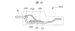
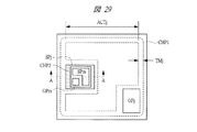
図3は、本実施の形態1におけるパッケージ(半導体装置)PKG1の実装構成を示す図である。図3に示すように、本実施の形態1におけるパッケージPKG1は、互いに電気的に絶縁された2つのチップ搭載部PLT1とチップ搭載部PLT2を有している。図3において、右側に配置されている金属プレートがチップ搭載部PLT1を構成し、左側に配置されている金属プレートがチップ搭載部PLT2を構成している。チップ搭載部PLT1は、ドレインリードDLと連結されるように一体的に形成されており、チップ搭載部PLT1とドレインリードDLとは電気的に接続されている。そして、このドレインリードDLを離間して挟むように、ソースリードSLとゲートリードGLが配置されている。具体的には、図3に示すように、ドレインリードDLの右側にソースリードSLが配置され、ドレインリードDLの左側にゲートリードGLが配置されている。これらのドレインリードDL、ソースリードSL、および、ゲートリードGLは、互いに電気的に絶縁されている。そして、ソースリードSLの先端部には、幅広領域からなるソースリードポスト部SPSTが形成され、ゲートリードGLの先端部には、幅広領域からなるゲートリードポスト部GPSTが形成されている。
<Mounting Configuration of Semiconductor Device in First Embodiment>
FIG. 3 is a diagram showing a mounting configuration of the package (semiconductor device) PKG1 in the first embodiment. As shown in FIG. 3, the package PKG1 in the first embodiment has two chip mounting portions PLT1 and PLT2 that are electrically insulated from each other. In FIG. 3, the metal plate arranged on the right side constitutes the chip mounting part PLT1, and the metal plate arranged on the left side constitutes the chip mounting part PLT2. The chip mounting part PLT1 is integrally formed so as to be connected to the drain lead DL, and the chip mounting part PLT1 and the drain lead DL are electrically connected. The source lead SL and the gate lead GL are arranged so as to sandwich the drain lead DL. Specifically, as shown in FIG. 3, the source lead SL is disposed on the right side of the drain lead DL, and the gate lead GL is disposed on the left side of the drain lead DL. The drain lead DL, the source lead SL, and the gate lead GL are electrically insulated from each other. A source lead post portion SPST made of a wide region is formed at the tip portion of the source lead SL, and a gate lead post portion GPST made of a wide region is formed at the tip portion of the gate lead GL.
次に、チップ搭載部PLT1上には、例えば、銀ペーストや半田からなる導電性接着材を介して、半導体チップCHP1が搭載されている。この半導体チップCHP1には、例えば、SiCを材料とした接合FETが形成されている。そして、半導体チップCHP1の裏面がドレイン電極となっており、半導体チップCHP1の表面(主面)にソースパッドSPjとゲートパッドGPjが形成されている。つまり、半導体チップCHP1には、カスコード接続方式をしたスイッチング素子の一部を構成する接合FETが形成されており、この接合FETのドレインと電気的に接続されるドレイン電極が半導体チップCHP1の裏面に形成され、接合FETのソースと電気的に接続されるソースパッドSPj、および、接合FETのゲート電極と電気的に接続されるゲートパッドGPjが半導体チップCHP1の表面に形成されている。 Next, the semiconductor chip CHP1 is mounted on the chip mounting portion PLT1 via a conductive adhesive made of, for example, silver paste or solder. For example, a junction FET made of SiC is formed on the semiconductor chip CHP1. The back surface of the semiconductor chip CHP1 serves as a drain electrode, and the source pad SPj and the gate pad GPj are formed on the front surface (main surface) of the semiconductor chip CHP1. In other words, the semiconductor chip CHP1 is formed with a junction FET that constitutes a part of a cascode-connected switching element, and a drain electrode electrically connected to the drain of the junction FET is formed on the back surface of the semiconductor chip CHP1. A source pad SPj formed and electrically connected to the source of the junction FET and a gate pad GPj electrically connected to the gate electrode of the junction FET are formed on the surface of the semiconductor chip CHP1.
続いて、チップ搭載部PLT2上には、例えば、銀ペーストや半田からなる導電性接着材を介して、半導体チップCHP2が搭載されている。この半導体チップCHP2には、例えば、Siを材料としたMOSFETが形成されている。このとき、半導体チップCHP2の裏面がドレイン電極となっており、半導体チップCHP2の表面(主面)にソースパッドSPmとゲートパッドGPmが形成されている。つまり、半導体チップCHP2には、カスコード接続方式をしたスイッチング素子の一部を構成するMOSFETが形成されており、このMOSFETのドレインと電気的に接続されるドレイン電極が半導体チップCHP2の裏面に形成され、MOSFETのソースと電気的に接続されるソースパッドSPm、および、MOSFETのゲート電極と電気的に接続されるゲートパッドGPmが半導体チップCHP2の表面に形成されている。 Subsequently, the semiconductor chip CHP2 is mounted on the chip mounting portion PLT2 via a conductive adhesive made of, for example, silver paste or solder. For example, a MOSFET made of Si is formed on the semiconductor chip CHP2. At this time, the back surface of the semiconductor chip CHP2 serves as a drain electrode, and the source pad SPm and the gate pad GPm are formed on the front surface (main surface) of the semiconductor chip CHP2 . In other words, the semiconductor chip CHP2 is formed with a MOSFET that constitutes a part of the switching element using the cascode connection method, and a drain electrode that is electrically connected to the drain of the MOSFET is formed on the back surface of the semiconductor chip CHP2. A source pad SPm electrically connected to the source of the MOSFET and a gate pad GPm electrically connected to the gate electrode of the MOSFET are formed on the surface of the semiconductor chip CHP2.
そして、チップ搭載部PLT1上に搭載された半導体チップCHP1と、チップ搭載部PLT2上に搭載された半導体チップCHP2と、ボンディングワイヤで接続することにより、カスコード接続されたスイッチング素子を構成することができる。具体的には、図3に示すように、半導体チップCHP1の表面に形成されているゲートパッドGPjと、ソースリードSLの先端部に形成されているソースリードポスト部SPSTがワイヤWgjで電気的に接続されている。また、半導体チップCHP1の表面に形成されているソースパッドSPjと、チップ搭載部PLT2がワイヤWdsで電気的に接続されている。さらに、半導体チップCHP2の表面に形成されているソースパッドSPmと、ソースリードSLの先端部に形成されているソースリードポスト部SPSTがワイヤWsmで電気的に接続されている。また、半導体チップCHP2の表面に形成されているゲートパッドGPmと、ゲートリードGLの先端部に形成されているゲートリードポスト部GPSTがワイヤWgmで電気的に接続されている。ここで、ソースリードポスト部SPSTのワイヤWgjおよびワイヤWsmが接続されている領域と、ゲートリードポスト部GPSTのワイヤWgmが接続されている領域は、チップ搭載部PLT1の上面やチップ搭載部PLT2の上面よりも高い位置に位置するように構成されている。 A cascode-connected switching element can be configured by connecting the semiconductor chip CHP1 mounted on the chip mounting portion PLT1 and the semiconductor chip CHP2 mounted on the chip mounting portion PLT2 with bonding wires. . Specifically, as shown in FIG. 3, the gate pad GPj formed on the surface of the semiconductor chip CHP1 and the source lead post part SPST formed at the tip of the source lead SL are electrically connected by a wire Wgj. It is connected. Further, the source pad SPj formed on the surface of the semiconductor chip CHP1 and the chip mounting part PLT2 are electrically connected by a wire Wds. Further, the source pad SPm formed on the surface of the semiconductor chip CHP2 and the source lead post portion SPST formed at the tip of the source lead SL are electrically connected by a wire Wsm. Further, the gate pad GPm formed on the surface of the semiconductor chip CHP2 and the gate lead post part GPST formed at the tip of the gate lead GL are electrically connected by a wire Wgm. Here, the region where the wire Wgj and the wire Wsm of the source lead post part SPST are connected and the region where the wire Wgm of the gate lead post part GPST is connected are the upper surface of the chip mounting part PLT1 and the chip mounting part PLT2. It is comprised so that it may be located in a position higher than an upper surface.
なお、半導体チップCHP1は、導電性接着材を介してチップ搭載部PLT1上に搭載されていることから、半導体チップCHP1の裏面に形成されているドレイン電極は、チップ搭載部PLT1と電気的に接続されている。また、半導体チップCHP2は、導電性接着材を介してチップ搭載部PLT2上に搭載されていることから、半導体チップCHP2の裏面に形成されているドレイン電極は、チップ搭載部PLT2と電気的に接続されていることになる。 Since the semiconductor chip CHP1 is mounted on the chip mounting portion PLT1 via a conductive adhesive, the drain electrode formed on the back surface of the semiconductor chip CHP1 is electrically connected to the chip mounting portion PLT1. Has been. Further, since the semiconductor chip CHP2 is mounted on the chip mounting portion PLT2 via a conductive adhesive, the drain electrode formed on the back surface of the semiconductor chip CHP2 is electrically connected to the chip mounting portion PLT2. Will be.
このように構成されているパッケージPKG1においては、半導体チップCHP1、半導体チップCHP2、チップ搭載部PLT1の一部、チップ搭載部PLT2の一部、ドレインリードDLの一部、ソースリードSLの一部、ゲートリードGLの一部、および、ワイヤWgj、Wds、Wgm、Wsmが、少なくとも、封止体で封止されている。したがって、チップ搭載部PLT1とチップ搭載部PLT2との間には、封止体の一部が配置されていることになり、これによって、チップ搭載部PLT1とチップ搭載部PLT2が封止体によって電気的に絶縁されることになる。なお、チップ搭載部PLT1の下面、および、チップ搭載部PLT2の下面は、封止体から露出するように構成されていてもよい。この場合、半導体チップCHP1や半導体チップCHP2で発生した熱を、チップ搭載部PLT1の下面やチップ搭載部PLT2の下面から効率良く放散させることができる。 In the package PKG1 configured in this way, the semiconductor chip CHP1, the semiconductor chip CHP2, a part of the chip mounting part PLT1, a part of the chip mounting part PLT2, a part of the drain lead DL, a part of the source lead SL, A part of the gate lead GL and the wires Wgj, Wds, Wgm, Wsm are at least sealed with a sealing body. Therefore, a part of the sealing body is arranged between the chip mounting part PLT1 and the chip mounting part PLT2, and thereby the chip mounting part PLT1 and the chip mounting part PLT2 are electrically connected by the sealing body. Will be electrically insulated. Note that the lower surface of the chip mounting portion PLT1 and the lower surface of the chip mounting portion PLT2 may be configured to be exposed from the sealing body. In this case, the heat generated in the semiconductor chip CHP1 and the semiconductor chip CHP2 can be efficiently dissipated from the lower surface of the chip mounting part PLT1 and the lower surface of the chip mounting part PLT2.
この封止体は、例えば、直方体形状をしており、第1側面と、この第1側面と対向する第2側面とを有している。この場合、例えば、封止体の第1側面から、ドレインリードDLの一部、ソースリードSLの一部、ゲートリードGLの一部が突出している。これらの突出したドレインリードDLの一部、ソースリードSLの一部、ゲートリードGLの一部が外部接続端子として機能することになる。 The sealing body has, for example, a rectangular parallelepiped shape, and has a first side surface and a second side surface facing the first side surface. In this case, for example, a part of the drain lead DL, a part of the source lead SL, and a part of the gate lead GL protrude from the first side surface of the sealing body. A part of the protruding drain lead DL, a part of the source lead SL, and a part of the gate lead GL function as external connection terminals.
ここで、カスコード接続されたスイッチング素子では、半導体チップCHP1と半導体チップCHP2という2つの半導体チップを搭載するため、パッケージ内に1つのチップ搭載部しか有さない既存の汎用パッケージをそのまま流用することはできない。例えば、数A以上の大きな定格電流での使用も考慮して、半導体チップCHP1に形成されている接合FETや、半導体チップCHP2に形成されているMOSFETは、いわゆる半導体チップの裏面にドレイン電極を有する縦型構造が採用されている。この場合、カスコード接続方式のスイッチング素子では、半導体チップCHP1の裏面に形成されているドレイン電極と、半導体チップCHP2の裏面に形成されているドレイン電極とを電気的に接続することはできない。このことから、パッケージ内に1つのチップ搭載部しか有さない既存の汎用パッケージにおいては、この1つのチップ搭載部に、半導体チップCHP1と半導体チップCHP2を配置すると、半導体チップCHP1の裏面に形成されているドレイン電極と、半導体チップCHP2の裏面に形成されているドレイン電極が電気的に接続されてしまいカスコード接続方式を実現することができなくなる。 Here, in the cascode-connected switching element, since two semiconductor chips, the semiconductor chip CHP1 and the semiconductor chip CHP2, are mounted, it is not possible to divert an existing general-purpose package having only one chip mounting portion in the package as it is. Can not. For example, considering the use with a large rated current of several A or more, the junction FET formed on the semiconductor chip CHP1 and the MOSFET formed on the semiconductor chip CHP2 have a drain electrode on the back surface of the so-called semiconductor chip. Vertical structure is adopted. In this case, in the cascode connection type switching element, the drain electrode formed on the back surface of the semiconductor chip CHP1 cannot be electrically connected to the drain electrode formed on the back surface of the semiconductor chip CHP2. For this reason, in the existing general-purpose package having only one chip mounting portion in the package, when the semiconductor chip CHP1 and the semiconductor chip CHP2 are arranged in this one chip mounting portion, they are formed on the back surface of the semiconductor chip CHP1. The drain electrode formed on the back surface of the semiconductor chip CHP2 is electrically connected to the cascode connection method.
そこで、本実施の形態1では、図3に示すように、外形形状が汎用パッケージと同等であることを前提として、封止体の内部に、互いに電気的に絶縁された2つのチップ搭載部PLT1およびチップ搭載部PLT2を設けるようにパッケージPKG1を構成している。そして、チップ搭載部PLT1上に半導体チップCHP1を搭載するとともに、チップ搭載部PLT2上に半導体チップCHP2を搭載するように、パッケージPKG1を構成している。つまり、電気的に絶縁された2つのチップ搭載部PLT1およびチップ搭載部PLT2をパッケージPKG1内に設け、半導体チップCHP1と半導体チップCHP2とを平面的に配置し、平面的に配置された半導体チップCHP1と半導体チップCHP2とをワイヤで接続することにより、カスコード接続を実現している。 Therefore, in the first embodiment, as shown in FIG. 3, two chip mounting portions PLT1 that are electrically insulated from each other inside the sealing body on the assumption that the outer shape is equivalent to that of the general-purpose package. The package PKG1 is configured so as to provide the chip mounting portion PLT2. The package PKG1 is configured such that the semiconductor chip CHP1 is mounted on the chip mounting portion PLT1, and the semiconductor chip CHP2 is mounted on the chip mounting portion PLT2. That is, two chip mounting portions PLT1 and PLT2 that are electrically insulated are provided in the package PKG1, the semiconductor chip CHP1 and the semiconductor chip CHP2 are arranged in a plane, and the semiconductor chip CHP1 arranged in a plane is arranged. The cascode connection is realized by connecting the semiconductor chip CHP2 to the semiconductor chip CHP2.
このため、本実施の形態1におけるパッケージPKG1によれば、例えば、電源回路などに利用されているスイッチング素子を実装している既存の汎用パッケージを、外形寸法の同等な本実施の形態1におけるパッケージPKG1に入れ替えることができる。特に、本実施の形態1におけるパッケージPKG1によれば、ドレインリードDL、ソースリードSL、および、ゲートリードGLの配置が汎用パッケージと同様であるため、汎用パッケージを本実施の形態1におけるパッケージPKG1に入れ替えることが可能であり、その他の駆動回路やプリント基板の配線などを設計変更する必要がない。したがって、本実施の形態1によれば、汎用パッケージを利用したスイッチング素子から、本実施の形態1のパッケージPKG1を利用した高性能なカスコード接続方式のスイッチング素子に変更することが容易であり、高性能な電源システムを大幅な設計変更することなく提供できるという利点を有している。 Therefore, according to the package PKG1 in the first embodiment, for example, an existing general-purpose package in which a switching element used for a power supply circuit or the like is mounted is replaced with a package in the first embodiment having the same outer dimensions. It can be replaced with PKG1. In particular, according to the package PKG1 in the first embodiment, since the arrangement of the drain lead DL, the source lead SL, and the gate lead GL is the same as that of the general-purpose package, the general-purpose package is changed to the package PKG1 in the first embodiment. It is possible to replace them, and it is not necessary to change the design of other driving circuits and printed circuit board wiring. Therefore, according to the first embodiment, it is easy to change from a switching element using a general-purpose package to a high-performance cascode connection switching element using the package PKG1 of the first embodiment. This has the advantage that a high-performance power supply system can be provided without significant design changes.
以下に、本実施の形態1におけるパッケージPKG1の特徴点について説明する。まず、本実施の形態1における第1特徴点は、図3に示すように、接合FETを形成した半導体チップCHP1の表面に設けられているゲートパッドGPjと、ソースリードSLとをできるだけ近づけるように配置する点にある。具体的に、本実施の形態1では、半導体チップCHP1を搭載するチップ搭載部PLT1をドレインリードDLに対してソースリードSLが配置されている側と同じ側に配置している。これにより、チップ搭載部PLT1をソースリードSLに近づけることができる。このことは、チップ搭載部PLT1上に搭載される半導体チップCHP1をソースリードSLに近づけるように配置できることを意味している。そして、本実施の形態1では、チップ搭載部PLT1上に搭載される半導体チップCHP1をチップ搭載部PLT1の中央部に配置するのではなく、チップ搭載部PLT1のソースリードSLに最も近い辺へ近づくように半導体チップCHP1を配置している。これにより、半導体チップCHP1をソースリードSLに最も近づくように配置することができる。さらに、本実施の形態1では、半導体チップCHP1をできるだけ、ソースリードSLに近づけるように配置するとともに、半導体チップCHP1の表面に形成されているゲートパッドGPjがソースリードSLに近づくように配置されている。このように本実施の形態1では、まず、接合FETが形成されている半導体チップCHP1が搭載されるチップ搭載部PLT1を、ソースリードSLに近い位置に配置し、さらに、チップ搭載部PLT1内の内部領域のうち、ソースリードSLに近い領域に半導体チップCHP1を搭載している。その上、本実施の形態1では、半導体チップCHP1の表面に形成されているゲートパッドGPjがソースリードSLに近づくように、ゲートパッドGPjを配置している。これにより、半導体チップCHP1の表面に形成されているゲートパッドGPjと、ソースリードSLとが近づくことになる。言い換えれば、本実施の形態1においては、半導体チップCHP1の表面に形成されているゲートパッドGPjが、その他のリード(ドレインリードDLやゲートリードGL)よりもソースリードSLに近づくように配置されていることになる。この結果、本実施の形態1によれば、ゲートパッドGPjとソースリードSLとの間の距離を短くすることができるため、ゲートパッドGPjとソースリードSLとを接続するワイヤWgjの長さを短くすることができる。特に、本実施の形態1では、ソースリードSLのうち、ゲートパッドGPjに近い先端部に存在する幅広のソースリードポスト部SPSTでワイヤWgjを接続する構成を取っているので、さらに、ワイヤWgjの長さを短くすることができる。ワイヤWgjの長さを短くできるということは、ワイヤWgjに存在する寄生インダクタンス(図2のLgi1やLgi2)を低減できることを意味する。つまり、本実施の形態1によれば、ワイヤWgjに存在する寄生インダクタンスを充分に低減できる。このことから、上述した第2のメカニズムによるMOSFETへの絶縁耐圧以上の電圧印加を抑制することができ、これによって、カスコード接続されたMOSFETのアバランシェ破壊を効果的に抑制することができる。この結果、本実施の形態1によれば、半導体装置の信頼性向上を図ることができる。
Below, the feature point of package PKG1 in this
続いて、本実施の形態1における第2特徴点について説明する。本実施の形態1における第2特徴点は、図3に示すように、MOSFETを形成した半導体チップCHP2の表面に設けられているゲートパッドGPmと、ゲートリードGLとをできるだけ近づけるように配置する点にある。具体的に、本実施の形態1では、半導体チップCHP2を搭載するチップ搭載部PLT2をドレインリードDLに対してゲートリードGLが配置されている側と同じ側に配置している。これにより、チップ搭載部PLT2をゲートリードGLに近づけることができる。このことは、チップ搭載部PLT2上に搭載される半導体チップCHP2をゲートリードGLに近づけるように配置できることを意味している。そして、本実施の形態1では、チップ搭載部PLT2上に搭載される半導体チップCHP2をチップ搭載部PLT2の中央部に配置するのではなく、チップ搭載部PLT2のゲートリードGLに最も近い辺へ近づくように半導体チップCHP2を配置している。これにより、半導体チップCHP2をゲートリードGLに最も近づくように配置することができる。さらに、本実施の形態1では、半導体チップCHP2をできるだけ、ゲートリードGLに近づけるように配置するとともに、半導体チップCHP2の表面に形成されているゲートパッドGPmがゲートリードGLに近づくように配置されている。このように本実施の形態1では、まず、MOSFETが形成されている半導体チップCHP2が搭載されるチップ搭載部PLT2を、ゲートリードGLに近い位置に配置し、さらに、チップ搭載部PLT2内の内部領域のうち、ゲートリードGLに近い領域に半導体チップCHP2を搭載している。その上、本実施の形態1では、半導体チップCHP2の表面に形成されているゲートパッドGPmがゲートリードGLに近づくように、ゲートパッドGPmを配置している。これにより、半導体チップCHP2の表面に形成されているゲートパッドGPmと、ゲートリードGLとが近づくことになる。言い換えれば、本実施の形態1においては、半導体チップCHP2の表面に形成されているゲートパッドGPmが、その他のリード(ドレインリードDLやソースリードSL)よりもゲートリードGLに近づくように配置されていることになる。この結果、本実施の形態1によれば、ゲートパッドGPmとゲートリードGLとの間の距離を短くすることができるため、ゲートパッドGPmとゲートリードGLとを接続するワイヤWgmの長さを短くすることができる。特に、本実施の形態1では、ゲートリードGLのうち、ゲートパッドGPmに近い先端部に存在する幅広のゲートリードポスト部GPSTでワイヤWgmを接続する構成を取っているので、さらに、ワイヤWgmの長さを短くすることができる。これにより、本実施の形態1によれば、ワイヤWgmの寄生インダクタンスを低減することができる。このワイヤWgmの寄生インダクタンスを低減できることは、カスコード接続されたスイッチング素子の電気的特性の向上に寄与するが、MOSFETへの絶縁耐圧以上の電圧印加を抑制することとは直接関連していない。本実施の形態1における第2特徴点の構成によれば、直接的ではなく間接的に、MOSFETへの絶縁耐圧以上の電圧印加を抑制できるのである。
Next, the second feature point in the first embodiment will be described. As shown in FIG. 3, the second feature point in the first embodiment is that the gate pad GPm provided on the surface of the semiconductor chip CHP2 on which the MOSFET is formed and the gate lead GL are arranged as close as possible. It is in. Specifically, in the first embodiment, the chip mounting part PLT2 for mounting the semiconductor chip CHP2 is disposed on the same side as the side on which the gate lead GL is disposed with respect to the drain lead DL. Thereby, the chip mounting part PLT2 can be brought close to the gate lead GL. This means that the semiconductor chip CHP2 mounted on the chip mounting portion PLT2 can be arranged so as to be close to the gate lead GL. In the first embodiment, the semiconductor chip CHP2 mounted on the chip mounting portion PLT2 is not disposed at the center of the chip mounting portion PLT2, but approaches the side closest to the gate lead GL of the chip mounting portion PLT2. Thus, the semiconductor chip CHP2 is arranged. Thereby, the semiconductor chip CHP2 can be arranged so as to be closest to the gate lead GL. Furthermore, in the first embodiment, the semiconductor chip CHP2 is arranged as close to the gate lead GL as possible, and the gate pad GPm formed on the surface of the semiconductor chip CHP2 is arranged so as to be close to the gate lead GL. Yes. As described above, in the first embodiment, first, the chip mounting portion PLT2 on which the semiconductor chip CHP2 on which the MOSFET is formed is mounted is disposed at a position close to the gate lead GL, and further, the inside of the chip mounting portion PLT2 Among the regions, the semiconductor chip CHP2 is mounted in a region close to the gate lead GL. Moreover, in the first embodiment, the gate pad GPm is arranged so that the gate pad GPm formed on the surface of the semiconductor chip CHP2 approaches the gate lead GL. As a result, the gate pad GPm formed on the surface of the semiconductor chip CHP2 and the gate lead GL approach each other. In other words, in the first embodiment, the gate pad GPm formed on the surface of the semiconductor chip CHP2 is arranged so as to be closer to the gate lead GL than the other leads (drain lead DL and source lead SL). Will be. As a result, according to the first embodiment, since the distance between the gate pad GPm and the gate lead GL can be shortened, the length of the wire Wgm connecting the gate pad GPm and the gate lead GL is shortened. can do. In particular, in the first embodiment, among the gate leads GL, the wire Wgm is connected by the wide gate lead post portion GPST present at the tip portion close to the gate pad GPm. The length can be shortened. Thereby, according to this
以下に、この点について説明する。図3に示すように、本実施の形態1における第2特徴点は、MOSFETが形成された半導体チップCHP2をできるだけ、ゲートリードGLに近づけるように配置する点にある。このことは、図3に示すように、チップ搭載部PLT2の手前側に偏って半導体チップCHP2が配置されることを意味し、言い換えれば、チップ搭載部PLT2の奥側に、半導体チップCHP2が搭載されていない大きなスペースができることを意味する。このように、本実施の形態1では、チップ搭載部PLT2に、半導体チップCHP2が搭載されていない大きなスペースを確保できる点に間接的な特徴がある。具体的には、この特徴により、図3に示すように、チップ搭載部PLT1上に搭載された半導体チップCHP1の表面に形成されているソースパッドSPjと、チップ搭載部PLT2とを電気的に接続するワイヤ接続領域を充分に確保することができるのである。この結果、図3に示すように、ソースパッドSPjとチップ搭載部PLT2とを複数本のワイヤWdsで接続できることになる。ここで、チップ搭載部PLT2は、搭載されている半導体チップCHP2の裏面に形成されているドレイン電極と電気的に接続されていることから、本実施の形態1によれば、複数本のワイヤWdsによって、MOSFETのドレインと接合FETのソースが接続されることになる。このことは、MOSFETのドレインと接合FETのソースとを接続するワイヤWdsの寄生インダクタンス(図2のLse1、Lse2)を低減できることを意味する。つまり、本実施の形態1によれば、複数本のワイヤWdsを使用することにより、MOSFETのドレインと接合FETのソース間の寄生インダクタンスを充分に低減できる。 This point will be described below. As shown in FIG. 3, the second feature point in the first embodiment is that the semiconductor chip CHP2 on which the MOSFET is formed is arranged as close to the gate lead GL as possible. This means that, as shown in FIG. 3, the semiconductor chip CHP2 is arranged to be biased toward the front side of the chip mounting part PLT2, in other words, the semiconductor chip CHP2 is mounted on the back side of the chip mounting part PLT2. It means that there can be a large space that is not. As described above, the first embodiment has an indirect feature in that a large space in which the semiconductor chip CHP2 is not mounted can be secured in the chip mounting portion PLT2. Specifically, due to this feature, as shown in FIG. 3, the source pad SPj formed on the surface of the semiconductor chip CHP1 mounted on the chip mounting portion PLT1 is electrically connected to the chip mounting portion PLT2. A sufficient wire connection area can be secured. As a result, as shown in FIG. 3, the source pad SPj and the chip mounting portion PLT2 can be connected by a plurality of wires Wds. Here, since the chip mounting portion PLT2 is electrically connected to the drain electrode formed on the back surface of the mounted semiconductor chip CHP2, according to the first embodiment, a plurality of wires Wds are provided. Thus, the drain of the MOSFET and the source of the junction FET are connected. This means that the parasitic inductance (Lse1, Lse2 in FIG. 2) of the wire Wds connecting the drain of the MOSFET and the source of the junction FET can be reduced. That is, according to the first embodiment, by using a plurality of wires Wds, the parasitic inductance between the drain of the MOSFET and the source of the junction FET can be sufficiently reduced.
さらには、図3に示すように、半導体チップCHP1の表面に形成されているソースパッドSPjの形成位置を、なるべく、チップ搭載部PLT2に近づけるように配置することが望ましい。なぜなら、ソースパッドSPjを、このように配置することにより、ソースパッドSPjとチップ搭載部PLT2とを接続するワイヤWdsの長さをできるだけ短くすることができるからである。これによっても、MOSFETのドレインと接合FETのソースとを接続するワイヤWdsの寄生インダクタンス(図2のLse1、Lse2)を低減できる。 Furthermore, as shown in FIG. 3, it is desirable that the formation position of the source pad SPj formed on the surface of the semiconductor chip CHP1 is as close as possible to the chip mounting portion PLT2. This is because by arranging the source pad SPj in this way, the length of the wire Wds connecting the source pad SPj and the chip mounting portion PLT2 can be made as short as possible. This also reduces the parasitic inductance (Lse1, Lse2 in FIG. 2) of the wire Wds connecting the drain of the MOSFET and the source of the junction FET.
以上のことから、本実施の形態1における第2特徴点によれば、上述した第1のメカニズムによるMOSFETへの絶縁耐圧以上の電圧印加を抑制することができ、これによって、カスコード接続されたMOSFETのアバランシェ破壊を効果的に抑制することができる。この結果、本実施の形態1によれば、半導体装置の信頼性向上を図ることができる。 From the above, according to the second feature point of the first embodiment, it is possible to suppress the voltage application over the withstand voltage to the MOSFET by the first mechanism described above, and thereby the cascode-connected MOSFET The avalanche destruction can be effectively suppressed. As a result, according to the first embodiment, the reliability of the semiconductor device can be improved.
なお、本実施の形態1では、図3に示すように、ゲートパッドGPjは、ワイヤWgjによって、ソースリードSLと電気的に接続され、かつ、ゲートパッドGPmは、ワイヤWgmによって、ゲートリードGLと電気的に接続されている。このとき、ワイヤWgjの太さ(幅)は、ワイヤWgmの太さ(幅)よりも太く構成することが望ましい。なぜなら、ワイヤWgjに存在する寄生抵抗が大きくなると、第3のメカニズムによって、MOSFETへ絶縁耐圧以上の電圧が印加されることになってしまうからである。したがって、ワイヤWgjに存在する寄生抵抗を低減する観点から、ワイヤWgjの太さをその他のワイヤよりも太くする構成を取ることが望ましい。これにより、接合FETのゲート電極とスイッチング素子のソース(MOSFETのソースということもできる)との間の寄生抵抗を低減できることから、上述した第3のメカニズムによるMOSFETへの絶縁耐圧以上の電圧印加を抑制することができ、これによって、カスコード接続されたMOSFETのアバランシェ破壊を効果的に抑制することができる。この結果、本実施の形態1によれば、半導体装置の信頼性向上を図ることができる。 In the first embodiment, as shown in FIG. 3, the gate pad GPj is electrically connected to the source lead SL by the wire Wgj, and the gate pad GPm is connected to the gate lead GL by the wire Wgm. Electrically connected. At this time, it is desirable that the thickness (width) of the wire Wgj is larger than the thickness (width) of the wire Wgm. This is because when the parasitic resistance existing in the wire Wgj is increased, a voltage exceeding the withstand voltage is applied to the MOSFET by the third mechanism. Therefore, it is desirable to make the wire Wgj thicker than other wires from the viewpoint of reducing the parasitic resistance existing in the wire Wgj. As a result, the parasitic resistance between the gate electrode of the junction FET and the source of the switching element (also referred to as the source of the MOSFET) can be reduced. Therefore, a voltage exceeding the withstand voltage is applied to the MOSFET by the third mechanism described above. Thus, the avalanche breakdown of the cascode-connected MOSFET can be effectively suppressed. As a result, according to the first embodiment, the reliability of the semiconductor device can be improved.
次に、本実施の形態1における第3特徴点について説明する。本実施の形態1における第3特徴点は、図3に示すように、MOSFETを形成した半導体チップCHP2の表面に設けられているソースパッドSPmと、ソースリードSL(ソースリードポスト部SPST)とを複数本のワイヤWsmで接続する点にある。これにより、MOSFETのソースとソースリードSLとの間の寄生抵抗および寄生インダクタンスを低減することができる。この結果、MOSFETのソースの電位がソースリードSLから供給されるGND電位(基準電位)から変動することを抑制でき、MOSFETのソースをGND電位に確実に固定することができる。さらには、MOSFETのソースとソースリードSLとの間の寄生抵抗が低減されることから、カスコード接続されたスイッチング素子のオン抵抗を低減することもできる。このように、本実施の形態1における第3特徴点によれば、パッケージPKG1に形成されているカスコード接続されたスイッチング素子の電気的特性の向上を図ることができる。 Next, the third feature point in the first embodiment will be described. As shown in FIG. 3, the third feature of the first embodiment is that the source pad SPm provided on the surface of the semiconductor chip CHP2 on which the MOSFET is formed and the source lead SL (source lead post portion SPST) are provided. The connection is made with a plurality of wires Wsm. Thereby, the parasitic resistance and the parasitic inductance between the source of the MOSFET and the source lead SL can be reduced. As a result, the source potential of the MOSFET can be prevented from fluctuating from the GND potential (reference potential) supplied from the source lead SL, and the source of the MOSFET can be reliably fixed to the GND potential. Furthermore, since the parasitic resistance between the source of the MOSFET and the source lead SL is reduced, the on-resistance of the cascode-connected switching element can also be reduced. As described above, according to the third feature point in the first embodiment, the electrical characteristics of the cascode-connected switching element formed in the package PKG1 can be improved.
以上のように、本実施の形態1におけるパッケージPKG1(半導体装置)によれば、上述した第1特徴点と第2特徴点を備えることにより、MOSFETへの絶縁耐圧以上の電圧印加を抑制することができ、これによって、カスコード接続されたMOSFETのアバランシェ破壊を効果的に抑制することができる。この結果、半導体装置の信頼性向上を図ることができる。さらには、本実施の形態1におけるパッケージPKG1(半導体装置)が上述した第3特徴点を備えることによっても、寄生抵抗および寄生インダクタンスの低減を図ることができることから、半導体装置の電気的特性の向上を図ることができる。 As described above, according to the package PKG1 (semiconductor device) in the first embodiment, by providing the first feature point and the second feature point described above, it is possible to suppress the voltage application to the MOSFET beyond the withstand voltage. Thus, the avalanche breakdown of the cascode-connected MOSFET can be effectively suppressed. As a result, the reliability of the semiconductor device can be improved. Furthermore, since the package PKG1 (semiconductor device) according to the first embodiment is provided with the third feature point described above, the parasitic resistance and the parasitic inductance can be reduced, so that the electrical characteristics of the semiconductor device are improved. Can be achieved.
また、本実施の形態1のパッケージPKG1に付随する具体的な効果として、本実施の形態1におけるパッケージPKG1は、接合FETを形成した半導体チップCHP1と、MOSFETを形成した半導体チップCHP2を平面的に配置する構成を採用しているので、半導体チップCHP1や半導体チップCHP2のチップ面積を自由に設計することができる。このことから、低オン抵抗の設計やオン電流密度の設計も容易となり、様々な仕様のスイッチング素子を実現することができる。 Further, as a specific effect accompanying the package PKG1 of the first embodiment, the package PKG1 in the first embodiment includes a semiconductor chip CHP1 in which a junction FET is formed and a semiconductor chip CHP2 in which a MOSFET is formed in a plane. Since the arrangement configuration is adopted, the chip areas of the semiconductor chip CHP1 and the semiconductor chip CHP2 can be freely designed. This facilitates the design of low on-resistance and on-current density, and can realize switching devices with various specifications.
続いて、本実施の形態1におけるスイッチング素子の他の実装形態の一例について説明する。図4は、本実施の形態1におけるパッケージPKG2の実装構成を示す図である。図4に示すパッケージPKG2と、図3に示すパッケージPKG1との相違点は、ソースリードSLとドレインリードDLの形成位置が異なる点である。具体的に、図3に示すパッケージPKG1では、一番左側にゲートリードGLが配置され、真中にドレインリードDLが配置され、一番右側にソースリードSLが配置されていた。これに対し、図4に示すパッケージPKG2では、一番左側にゲートリードGLが配置され、真中にソースリードSLが配置され、一番右側にドレインリードDLが配置されている。この場合、図4に示すように、ソースリードSLの配置位置が変更されていることに伴って、半導体チップCHP1の表面に形成されているゲートパッドGPjの形成位置も、他のリードよりもソースリードSLに近くなるように変更されている。この結果、図4に示すパッケージPKG2においても、ゲートパッドGPjとソースリードSLとの間の距離を短くすることができる。このため、ゲートパッドGPjとソースリードSLとを接続するワイヤWgjの長さを短くすることができる。つまり、図4に示すパッケージPKG2においても、ワイヤWgjに存在する寄生インダクタンスを充分に低減できる。このことから、上述した第2のメカニズムによるMOSFETへの絶縁耐圧以上の電圧印加を抑制することができ、これによって、カスコード接続されたMOSFETのアバランシェ破壊を効果的に抑制することができる。この結果、図4に示すパッケージPKG2においても、半導体装置の信頼性向上を図ることができる。 Subsequently, an example of another mounting form of the switching element according to the first embodiment will be described. FIG. 4 is a diagram showing a mounting configuration of the package PKG2 in the first embodiment. The difference between the package PKG2 shown in FIG. 4 and the package PKG1 shown in FIG. 3 is that the formation positions of the source lead SL and the drain lead DL are different. Specifically, in the package PKG1 shown in FIG. 3, the gate lead GL is disposed on the leftmost side, the drain lead DL is disposed in the middle, and the source lead SL is disposed on the rightmost side. On the other hand, in the package PKG2 shown in FIG. 4, the gate lead GL is arranged on the leftmost side, the source lead SL is arranged in the middle, and the drain lead DL is arranged on the rightmost side. In this case, as shown in FIG. 4, as the arrangement position of the source lead SL is changed, the formation position of the gate pad GPj formed on the surface of the semiconductor chip CHP1 is also more source than the other leads. It has been changed to be closer to the lead SL. As a result, also in the package PKG2 shown in FIG. 4, the distance between the gate pad GPj and the source lead SL can be shortened. For this reason, the length of the wire Wgj connecting the gate pad GPj and the source lead SL can be shortened. That is, also in the package PKG2 shown in FIG. 4, the parasitic inductance existing in the wire Wgj can be sufficiently reduced. From this, it is possible to suppress the voltage application to or higher than the withstand voltage to the MOSFET by the second mechanism described above, and thereby it is possible to effectively suppress the avalanche breakdown of the cascode-connected MOSFET. As a result, the reliability of the semiconductor device can be improved also in the package PKG2 shown in FIG.
さらに、図4に示すパッケージPKG2に特有な特徴点としては、半導体チップCHP2の表面に形成されているソースパッドSPmと、ソースリードSLとを電気的に接続するワイヤWsmの長さを、図3に示すパッケージPKG1に比べて充分に短くすることができる点である。このため、図4に示すパッケージPKG2によれば、ワイヤWsmの寄生抵抗および寄生インダクタンスを低減できることから、本実施の形態1におけるスイッチング素子の電気的特性を向上させることができる。特に、ワイヤWsmの長さを短くすることによる効果は、本実施の形態1におけるスイッチング素子のオン抵抗を小さくなる点に顕在化する。 Furthermore, as a characteristic point peculiar to the package PKG2 shown in FIG. 4, the length of the wire Wsm that electrically connects the source pad SPm formed on the surface of the semiconductor chip CHP2 and the source lead SL is shown in FIG. This is a point that can be sufficiently shortened as compared with the package PKG1 shown in FIG. Therefore, according to the package PKG2 shown in FIG. 4, since the parasitic resistance and the parasitic inductance of the wire Wsm can be reduced, the electrical characteristics of the switching element according to the first embodiment can be improved. In particular, the effect of shortening the length of the wire Wsm becomes apparent in that the on-resistance of the switching element in the first embodiment is reduced.
<変形例1>
次に、本変形例1におけるパッケージPKG3の実装構成について説明する。本変形例1では、接合FETを形成した半導体チップと、MOSFETを形成した半導体チップとを積層する構成について説明する。
<
Next, the mounting configuration of the package PKG3 in the first modification will be described. In the first modification, a configuration in which a semiconductor chip on which a junction FET is formed and a semiconductor chip on which a MOSFET is formed will be described.
図5は、本変形例1におけるパッケージPKG3の実装構成を示す図である。図5において、本変形例1におけるパッケージPKG3は、例えば、矩形形状をした金属プレートからなるチップ搭載部PLTを有している。このチップ搭載部PLTは、ドレインリードDLと連結されるように一体的に形成されており、チップ搭載部PLTとドレインリードDLとは電気的に接続されている。そして、このドレインリードDLを離間して挟むように、ソースリードSLとゲートリードGLが配置されている。具体的には、図5に示すように、ドレインリードDLの右側にソースリードSLが配置され、ドレインリードDLの左側にゲートリードGLが配置されている。これらのドレインリードDL、ソースリードSL、および、ゲートリードGLは、互いに電気的に絶縁されている。そして、ソースリードSLの先端部には、幅広領域からなるソースリードポスト部SPSTが形成され、ゲートリードGLの先端部には、幅広領域からなるゲートリードポスト部GPSTが形成されている。 FIG. 5 is a diagram showing a mounting configuration of the package PKG3 in the first modification. In FIG. 5 , the package PKG3 in the first modification has a chip mounting portion PLT made of, for example, a rectangular metal plate. The chip mounting portion PLT is integrally formed so as to be connected to the drain lead DL, and the chip mounting portion PLT and the drain lead DL are electrically connected. The source lead SL and the gate lead GL are arranged so as to sandwich the drain lead DL. Specifically, as shown in FIG. 5, the source lead SL is arranged on the right side of the drain lead DL, and the gate lead GL is arranged on the left side of the drain lead DL. The drain lead DL, the source lead SL, and the gate lead GL are electrically insulated from each other. A source lead post portion SPST made of a wide region is formed at the tip portion of the source lead SL, and a gate lead post portion GPST made of a wide region is formed at the tip portion of the gate lead GL.
次に、チップ搭載部PLT上には、例えば、銀ペーストや半田からなる導電性接着材を介して、半導体チップCHP1が搭載されている。この半導体チップCHP1には、例えば、SiCを材料とした接合FETが形成されている。そして、半導体チップCHP1の裏面がドレイン電極となっており、半導体チップCHP1の表面(主面)にソースパッドSPjとゲートパッドGPjが形成されている。つまり、半導体チップCHP1には、カスコード接続方式をしたスイッチング素子の一部を構成する接合FETが形成されており、この接合FETのドレインと電気的に接続されるドレイン電極が半導体チップCHP1の裏面に形成され、接合FETのソースと電気的に接続されるソースパッドSPj、および、接合FETのゲート電極と電気的に接続されるゲートパッドGPjが半導体チップCHP1の表面に形成されている。 Next, the semiconductor chip CHP1 is mounted on the chip mounting portion PLT via a conductive adhesive made of, for example, silver paste or solder. For example, a junction FET made of SiC is formed on the semiconductor chip CHP1. The back surface of the semiconductor chip CHP1 serves as a drain electrode, and the source pad SPj and the gate pad GPj are formed on the front surface (main surface) of the semiconductor chip CHP1. In other words, the semiconductor chip CHP1 is formed with a junction FET that constitutes a part of a cascode-connected switching element, and a drain electrode electrically connected to the drain of the junction FET is formed on the back surface of the semiconductor chip CHP1. A source pad SPj formed and electrically connected to the source of the junction FET and a gate pad GPj electrically connected to the gate electrode of the junction FET are formed on the surface of the semiconductor chip CHP1.
続いて、この半導体チップCHP1上に、例えば、銀ペーストや半田からなる導電性接着材を介して、半導体チップCHP2が搭載されている。この半導体チップCHP2には、例えば、Siを材料としたMOSFETが形成されている。このとき、半導体チップCHP2の裏面がドレイン電極となっており、半導体チップCHP1の表面(主面)にソースパッドSPmとゲートパッドGPmが形成されている。つまり、半導体チップCHP2には、カスコード接続方式をしたスイッチング素子の一部を構成するMOSFETが形成されており、このMOSFETのドレインと電気的に接続されるドレイン電極が半導体チップCHP2の裏面に形成され、MOSFETのソースと電気的に接続されるソースパッドSPm、および、MOSFETのゲート電極と電気的に接続されるゲートパッドGPmが半導体チップCHP2の表面に形成されている。 Subsequently, the semiconductor chip CHP2 is mounted on the semiconductor chip CHP1 via a conductive adhesive made of, for example, silver paste or solder. For example, a MOSFET made of Si is formed on the semiconductor chip CHP2. At this time, the back surface of the semiconductor chip CHP2 serves as a drain electrode, and the source pad SPm and the gate pad GPm are formed on the front surface (main surface) of the semiconductor chip CHP1. In other words, the semiconductor chip CHP2 is formed with a MOSFET that constitutes a part of the switching element using the cascode connection method, and a drain electrode that is electrically connected to the drain of the MOSFET is formed on the back surface of the semiconductor chip CHP2. A source pad SPm electrically connected to the source of the MOSFET and a gate pad GPm electrically connected to the gate electrode of the MOSFET are formed on the surface of the semiconductor chip CHP2.
このように、本変形例1では、半導体チップCHP1上に半導体チップCHP2が搭載されており、特に、半導体チップCHP1の表面に形成されているソースパッドSPj上に半導体チップCHP2が搭載されている。これにより、半導体チップCHP2の裏面に形成されているドレイン電極と、半導体チップCHP1の表面に形成されているソースパッドSPjとが電気的に接続されることになる。この結果、半導体チップCHP1に形成されている接合FETのソースと、半導体チップCHP2に形成されているMOSFETのドレインとが電気的に接続されることになる。このことから、半導体チップCHP2は、平面視において、半導体チップCHP1の表面に形成されているソースパッドSPjに内包されるように形成されている必要がある。つまり、本変形例1においては、半導体チップCHP2のサイズは、半導体チップCHP1のサイズよりも小さくなっている必要があり、さらに言えば、半導体チップCHP2のサイズは、ソースパッドSPjのサイズよりも小さくなっている必要がある。 As described above, in the first modification, the semiconductor chip CHP2 is mounted on the semiconductor chip CHP1, and in particular, the semiconductor chip CHP2 is mounted on the source pad SPj formed on the surface of the semiconductor chip CHP1. As a result, the drain electrode formed on the back surface of the semiconductor chip CHP2 and the source pad SPj formed on the surface of the semiconductor chip CHP1 are electrically connected. As a result, the source of the junction FET formed in the semiconductor chip CHP1 and the drain of the MOSFET formed in the semiconductor chip CHP2 are electrically connected. Therefore, the semiconductor chip CHP2 needs to be formed so as to be included in the source pad SPj formed on the surface of the semiconductor chip CHP1 in plan view. That is, in the first modification, the size of the semiconductor chip CHP2 needs to be smaller than the size of the semiconductor chip CHP1, and more specifically, the size of the semiconductor chip CHP2 is smaller than the size of the source pad SPj. It needs to be.
続いて、図5に示すように、半導体チップCHP1の表面に形成されているゲートパッドGPjと、ソースリードSLの先端部に形成されているソースリードポスト部SPSTがワイヤWgjで電気的に接続されている。そして、半導体チップCHP2の表面に形成されているソースパッドSPmと、ソースリードSLの先端部に形成されているソースリードポスト部SPSTがワイヤWsmで電気的に接続されている。また、半導体チップCHP2の表面に形成されているゲートパッドGPmと、ゲートリードGLの先端部に形成されているゲートリードポスト部GPSTがワイヤWgmで電気的に接続されている。ここで、ソースリードポスト部SPSTのワイヤWgjおよびワイヤWsmが接続されている領域と、ゲートリードポスト部GPSTのワイヤWgmが接続されている領域は、チップ搭載部PLT1の上面やチップ搭載部PLT2の上面よりも高い位置に位置するように構成されている。 Subsequently, as shown in FIG. 5, the gate pad GPj formed on the surface of the semiconductor chip CHP1 and the source lead post part SPST formed at the tip of the source lead SL are electrically connected by the wire Wgj. ing. The source pad SPm formed on the surface of the semiconductor chip CHP2 and the source lead post portion SPST formed at the tip of the source lead SL are electrically connected by a wire Wsm. Further, the gate pad GPm formed on the surface of the semiconductor chip CHP2 and the gate lead post part GPST formed at the tip of the gate lead GL are electrically connected by a wire Wgm. Here, the region where the wire Wgj and the wire Wsm of the source lead post part SPST are connected and the region where the wire Wgm of the gate lead post part GPST is connected are the upper surface of the chip mounting part PLT1 and the chip mounting part PLT2. It is comprised so that it may be located in a position higher than an upper surface.
このように構成されているパッケージPKG3においては、半導体チップCHP1、半導体チップCHP2、チップ搭載部PLTの一部、ドレインリードDLの一部、ソースリードSLの一部、ゲートリードGLの一部、および、ワイヤWgj、Wgm、Wsmが、少なくとも、封止体で封止されている。なお、チップ搭載部PLTの下面は、封止体から露出するように構成されていてもよい。この場合、半導体チップCHP1や半導体チップCHP2で発生した熱を、チップ搭載部PLTの下面から効率良く放散させることができる。 In the package PKG3 thus configured, the semiconductor chip CHP1, the semiconductor chip CHP2, a part of the chip mounting part PLT, a part of the drain lead DL, a part of the source lead SL, a part of the gate lead GL, and The wires Wgj, Wgm, and Wsm are at least sealed with a sealing body. Note that the lower surface of the chip mounting portion PLT may be configured to be exposed from the sealing body. In this case, the heat generated in the semiconductor chip CHP1 and the semiconductor chip CHP2 can be efficiently dissipated from the lower surface of the chip mounting portion PLT.
この封止体は、例えば、直方体形状をしており、第1側面と、この第1側面と対向する第2側面とを有している。この場合、例えば、封止体の第1側面から、ドレインリードDLの一部、ソースリードSLの一部、ゲートリードGLの一部が突出している。これらの突出したドレインリードDLの一部、ソースリードSLの一部、ゲートリードGLの一部が外部接続端子として機能することになる。 The sealing body has, for example, a rectangular parallelepiped shape, and has a first side surface and a second side surface facing the first side surface. In this case, for example, a part of the drain lead DL, a part of the source lead SL, and a part of the gate lead GL protrude from the first side surface of the sealing body. A part of the protruding drain lead DL, a part of the source lead SL, and a part of the gate lead GL function as external connection terminals.
本変形例1におけるパッケージPKG3は上記のように構成されており、以下に、本変形例1におけるパッケージPKG3の特徴点について説明する。まず、本変形例1における特徴点は、図5に示すように、接合FETを形成した半導体チップCHP1の表面に設けられているゲートパッドGPjと、ソースリードSLとをできるだけ近づけるように配置する点にある。具体的に、本変形例1では、半導体チップCHP1をドレインリードDLに対してソースリードSLが配置されている側と同じ側に配置している。つまり、半導体チップCHP1は、図5に示す中心線a−a´に対して右側に偏って配置されている。これにより、半導体チップCHP1をソースリードSLに近づけることができる。そして、本変形例1では、半導体チップCHP1をチップ搭載部PLTの中央部に配置するのではなく、チップ搭載部PLTのソースリードSLに最も近い辺へ近づくように半導体チップCHP1を配置している。つまり、半導体チップCHP1は、図5に示す中心線b−b´に対して手前側(下側)に偏って配置されている。これにより、半導体チップCHP1をソースリードSLに最も近づくように配置することができる。言い換えれば、本変形例1においては、半導体チップCHP1の表面に形成されているゲートパッドGPjが、その他のリード(ドレインリードDLやゲートリードGL)よりもソースリードSLに近づくように配置されていることになる。この結果、本変形例1によれば、ゲートパッドGPjとソースリードSLとの間の距離を短くすることができるため、ゲートパッドGPjとソースリードSLとを接続するワイヤWgjの長さを短くすることができる。特に、本変形例1では、ソースリードSLのうち、ゲートパッドGPjに近い先端部に存在する幅広のソースリードポスト部SPSTでワイヤWgjを接続する構成を取っているので、さらに、ワイヤWgjの長さを短くすることができる。ワイヤWgjの長さを短くできるということは、ワイヤWgjに存在する寄生インダクタンス(図2のLgi1やLgi2)を低減できることを意味する。すなわち、本変形例1によれば、ワイヤWgjに存在する寄生インダクタンスを充分に低減できる。このことから、上述した第2のメカニズムによるMOSFETへの絶縁耐圧以上の電圧印加を抑制することができ、これによって、カスコード接続されたMOSFETのアバランシェ破壊を効果的に抑制することができる。この結果、本変形例1によれば、半導体装置の信頼性向上を図ることができる。 The package PKG3 in the first modification example is configured as described above, and the characteristic points of the package PKG3 in the first modification example will be described below. First, as shown in FIG. 5, the characteristic point in the first modification is that the gate pad GPj provided on the surface of the semiconductor chip CHP1 on which the junction FET is formed and the source lead SL are arranged as close as possible. It is in. Specifically, in the first modification, the semiconductor chip CHP1 is arranged on the same side as the side on which the source lead SL is arranged with respect to the drain lead DL. That is, the semiconductor chip CHP1 is arranged to be shifted to the right side with respect to the center line aa ′ shown in FIG. Thereby, the semiconductor chip CHP1 can be brought close to the source lead SL. In the first modification, the semiconductor chip CHP1 is not disposed at the center of the chip mounting portion PLT, but the semiconductor chip CHP1 is disposed so as to approach the side closest to the source lead SL of the chip mounting portion PLT. . That is, the semiconductor chip CHP1 is arranged so as to be biased toward the near side (lower side) with respect to the center line bb ′ shown in FIG. Thereby, the semiconductor chip CHP1 can be arranged so as to be closest to the source lead SL. In other words, in the first modification, the gate pad GPj formed on the surface of the semiconductor chip CHP1 is disposed so as to be closer to the source lead SL than the other leads (drain lead DL and gate lead GL). It will be. As a result, according to the first modification, since the distance between the gate pad GPj and the source lead SL can be shortened, the length of the wire Wgj connecting the gate pad GPj and the source lead SL is shortened. be able to. In particular, in the first modification, the wire Wgj is connected to the source lead SL by the wide source lead post portion SPST existing at the tip portion close to the gate pad GPj, and therefore, the length of the wire Wgj is further increased. The length can be shortened. The fact that the length of the wire Wgj can be shortened means that the parasitic inductance (Lgi1 and Lgi2 in FIG. 2) existing in the wire Wgj can be reduced. That is, according to the first modification, the parasitic inductance existing in the wire Wgj can be sufficiently reduced. From this, it is possible to suppress the voltage application to or higher than the withstand voltage to the MOSFET by the second mechanism described above, and thereby it is possible to effectively suppress the avalanche breakdown of the cascode-connected MOSFET. As a result, according to the first modification, the reliability of the semiconductor device can be improved.
ここで、ゲートパッドGPjとソースリードSLとを接続するワイヤWgjの長さを短くする観点からは、半導体チップCHP1のソースリードSLに最も近い辺側に、ゲートパッドGPjを偏って配置することが考えられる。ところが、本変形例1では、図5に示すように、半導体チップCHP1の右辺側に沿うとともに、右辺中央部に対して対称となるように、ゲートパッドGPjが配置されている。これは、以下に示す理由による。すなわち、ゲートパッドGPjは、半導体チップCHP1の内部に形成されている複数の接合FETの各ゲート電極とゲート配線によって接続されている。このことから、例えば、ゲートパッドGPjを右辺中央部に対して対称となるように配置することにより、複数の接合FETの各ゲート電極とゲートパッドGPjを接続するゲート配線の距離のばらつきを抑制できるのである。このことは、半導体チップCHP1内に形成されている複数の接合FETの特性を揃えて利用できることを意味している。このような理由から、本変形例1では、半導体チップCHP1の右辺中央部に対して対称となるように、ゲートパッドGPjを配置しているのである。 Here, from the viewpoint of shortening the length of the wire Wgj connecting the gate pad GPj and the source lead SL, the gate pad GPj may be biased on the side closest to the source lead SL of the semiconductor chip CHP1. Conceivable. However, in the first modification, as shown in FIG. 5, the gate pad GPj is arranged along the right side of the semiconductor chip CHP1 and symmetrical with respect to the center of the right side. This is due to the following reason. That is, the gate pad GPj is connected to each gate electrode of the plurality of junction FETs formed inside the semiconductor chip CHP1 by the gate wiring. From this, for example, by arranging the gate pad GPj so as to be symmetric with respect to the central portion on the right side, it is possible to suppress variations in the distance of the gate wiring connecting each gate electrode of the plurality of junction FETs and the gate pad GPj. It is. This means that the characteristics of a plurality of junction FETs formed in the semiconductor chip CHP1 can be used together. For this reason, in the first modification, the gate pad GPj is arranged so as to be symmetric with respect to the central portion on the right side of the semiconductor chip CHP1.
なお、本変形例1では、図5に示すように、ゲートパッドGPjは、ワイヤWgjによって、ソースリードSLと電気的に接続され、かつ、ゲートパッドGPmは、ワイヤWgmによって、ゲートリードGLと電気的に接続されている。このとき、ワイヤWgjの太さ(幅)は、ワイヤWgmの太さ(幅)よりも太く構成することが望ましい。なぜなら、ワイヤWgjに存在する寄生抵抗が大きくなると、第3のメカニズムによって、MOSFETへ絶縁耐圧以上の電圧が印加されることになってしまうからである。したがって、ワイヤWgjに存在する寄生抵抗を低減する観点から、ワイヤWgjの太さをその他のワイヤよりも太くする構成を取ることが望ましい。これにより、接合FETのゲート電極とスイッチング素子のソース(MOSFETのソースということもできる)との間の寄生抵抗を低減できることから、上述した第3のメカニズムによるMOSFETへの絶縁耐圧以上の電圧印加を抑制することができ、これによって、カスコード接続されたMOSFETのアバランシェ破壊を効果的に抑制することができる。この結果、本変形例1によれば、半導体装置の信頼性向上を図ることができる。 In the first modification, as shown in FIG. 5, the gate pad GPj is electrically connected to the source lead SL by the wire Wgj, and the gate pad GPm is electrically connected to the gate lead GL by the wire Wgm. Connected. At this time, it is desirable that the thickness (width) of the wire Wgj is larger than the thickness (width) of the wire Wgm. This is because when the parasitic resistance existing in the wire Wgj is increased, a voltage exceeding the withstand voltage is applied to the MOSFET by the third mechanism. Therefore, it is desirable to make the wire Wgj thicker than other wires from the viewpoint of reducing the parasitic resistance existing in the wire Wgj. As a result, the parasitic resistance between the gate electrode of the junction FET and the source of the switching element (also referred to as the source of the MOSFET) can be reduced. Therefore, a voltage exceeding the withstand voltage is applied to the MOSFET by the third mechanism described above. Thus, the avalanche breakdown of the cascode-connected MOSFET can be effectively suppressed. As a result, according to the first modification, the reliability of the semiconductor device can be improved.
次に、本変形例1におけるさらなる特徴点について説明する。本変形例1におけるさらなる特徴点は、図5に示すように、MOSFETを形成した半導体チップCHP2の表面に設けられているソースパッドSPmと、ソースリードSL(ソースリードポスト部SPST)とを複数本のワイヤWsmで接続する点にある。これにより、MOSFETのソースとソースリードSLとの間の寄生抵抗および寄生インダクタンスを低減することができる。この結果、MOSFETのソースの電位がソースリードSLから供給されるGND電位(基準電位)から変動することを抑制でき、MOSFETのソースをGND電位に確実に固定することができる。さらには、MOSFETのソースとソースリードSLとの間の寄生抵抗が低減されることから、カスコード接続されたスイッチング素子のオン抵抗を低減することもできる。このように、本変形例1におけるさらなる特徴点によれば、パッケージPKG3に形成されているカスコード接続されたスイッチング素子の電気的特性の向上を図ることができる。 Next, further feature points in the first modification will be described. As shown in FIG. 5, a further feature point of the first modification is that a plurality of source pads SPm and source leads SL (source lead post portions SPST) provided on the surface of the semiconductor chip CHP2 on which the MOSFET is formed are provided. It is in the point connected by the wire Wsm. Thereby, the parasitic resistance and the parasitic inductance between the source of the MOSFET and the source lead SL can be reduced. As a result, the source potential of the MOSFET can be prevented from fluctuating from the GND potential (reference potential) supplied from the source lead SL, and the source of the MOSFET can be reliably fixed to the GND potential. Furthermore, since the parasitic resistance between the source of the MOSFET and the source lead SL is reduced, the on-resistance of the cascode-connected switching element can also be reduced. As described above, according to the further feature point of the first modification, the electrical characteristics of the cascode-connected switching element formed in the package PKG3 can be improved.
続いて、本変形例1に特有の特徴点について説明する。本変形例1に特有の特徴点は、図5に示すように、接合FETを形成した半導体チップCHP1上に、MOSFETを形成した半導体チップCHP2が搭載されている点である。これにより、半導体チップCHP1の表面に形成されているソースパッドSPjと、半導体チップCHP2の裏面に形成されているドレイン電極とを直接接続することができる。つまり、本変形例1によれば、接合FETのソースと、MOSFETのドレインとをワイヤを使用せずに、直接接続することができる。このことは、接合FETのソースと、MOSFETのドレインとの間に介在する寄生インダクタンスをほぼ完全に削除できることを意味する。すなわち、本変形例1に特有の特徴点は、半導体チップCHP1上に直接半導体チップCHP2を搭載している点にあり、この構成によって、接合FETのソースと、MOSFETのドレインとを接続するためにワイヤが不要となるのである。ワイヤを使用する場合、ワイヤに存在する寄生インダクタンスが問題となるが、本変形例1によれば、ワイヤを使用せずに、接合FETのソースと、MOSFETのドレインとを直接接続することができるので、MOSFETのドレインと接合FETのソースとの間の寄生インダクタンス(図2のLse1、Lse2)をほぼ完全になくすことができる。以上のことから、本変形例1に特有の特徴点によれば、上述した第1のメカニズムによるMOSFETへの絶縁耐圧以上の電圧印加を抑制することができ、これによって、カスコード接続されたMOSFETのアバランシェ破壊を効果的に抑制することができる。この結果、本変形例1によれば、半導体装置の信頼性向上を図ることができる。 Subsequently, characteristic points unique to the first modification will be described. As shown in FIG. 5, the characteristic feature of the first modification is that a semiconductor chip CHP2 in which a MOSFET is formed is mounted on a semiconductor chip CHP1 in which a junction FET is formed. Thereby, the source pad SPj formed on the surface of the semiconductor chip CHP1 and the drain electrode formed on the back surface of the semiconductor chip CHP2 can be directly connected. That is, according to the first modification, the source of the junction FET and the drain of the MOSFET can be directly connected without using a wire. This means that the parasitic inductance interposed between the source of the junction FET and the drain of the MOSFET can be almost completely eliminated. That is, the characteristic feature unique to the first modification is that the semiconductor chip CHP2 is directly mounted on the semiconductor chip CHP1, and this configuration is used to connect the source of the junction FET and the drain of the MOSFET. This eliminates the need for wires. When a wire is used, parasitic inductance existing in the wire becomes a problem. According to the first modification, the source of the junction FET and the drain of the MOSFET can be directly connected without using the wire. Therefore, the parasitic inductance (Lse1, Lse2 in FIG. 2) between the drain of the MOSFET and the source of the junction FET can be almost completely eliminated. From the above, according to the characteristic feature unique to the first modification, it is possible to suppress the voltage application over the withstand voltage to the MOSFET by the first mechanism described above, and thereby, the cascode-connected MOSFET Avalanche destruction can be effectively suppressed. As a result, according to the first modification, the reliability of the semiconductor device can be improved.
本変形例1におけるパッケージPKG3によれば、チップ搭載部PLT上に半導体チップCHP1と半導体チップCHP2とを積層して配置している。このことから、本変形例1におけるパッケージPKG3では、パッケージ内に1つのチップ搭載部PLTを有する構造でもよく、したがって、パッケージ内に1つのチップ搭載部しか有さない既存の汎用パッケージをそのまま流用することができる。すなわち、本変形例1におけるパッケージPKG3によれば、いわゆる安価な汎用パッケージをそのまま流用することができるため、カスコード接続された高性能なスイッチング素子を安価に提供することができる。言い換えれば、本変形例1によれば、カスコード接続された高性能なスイッチング素子を形成したパッケージPKG3のコスト削減を図ることができる。 According to the package PKG3 in the first modification, the semiconductor chip CHP1 and the semiconductor chip CHP2 are stacked on the chip mounting portion PLT. From this, the package PKG3 in the first modification may have a structure having one chip mounting portion PLT in the package, and therefore, an existing general-purpose package having only one chip mounting portion in the package is used as it is. be able to. That is, according to the package PKG3 in the first modification, since a so-called inexpensive general-purpose package can be used as it is, a high-performance switching element connected in cascode can be provided at low cost. In other words, according to the first modification, it is possible to reduce the cost of the package PKG3 in which the cascode-connected high-performance switching element is formed.
また、本変形例1によれば、接合FETを形成した半導体チップCHP1と、MOSFETを形成した半導体チップCHP2とを積層しているため、半導体チップの実装面積を低減できる利点も得られる。特に、この場合、図5に示すように、チップ搭載部PLTに大きなスペースを確保することができるため、半導体チップCHP1や半導体チップCHP2で発生した熱を効率良く放散することもできる。さらには、本変形例1によれば、スイッチング素子の実装面積を低減することができるため、従来は、パッケージ外部のプリント基板上に配置していたフリーホイールダイオード(還流ダイオード)を、スイッチング素子と一緒のパッケージに実装できる利点も得られる。この結果、本変形例1によれば、プリント基板の実装面積削減にも寄与することができ、これによって、電源システムに代表されるシステム全体のコスト削減を図ることができる。 Further, according to the first modification, since the semiconductor chip CHP1 in which the junction FET is formed and the semiconductor chip CHP2 in which the MOSFET is formed are stacked, there is also an advantage that the mounting area of the semiconductor chip can be reduced. In particular, in this case, as shown in FIG. 5, since a large space can be secured in the chip mounting portion PLT, heat generated in the semiconductor chip CHP1 and the semiconductor chip CHP2 can also be efficiently dissipated. Furthermore, according to the first modification, since the mounting area of the switching element can be reduced, conventionally, a free wheel diode (freewheeling diode) arranged on a printed circuit board outside the package is replaced with a switching element. There is also an advantage that it can be mounted in the same package. As a result, according to the first modification, it is possible to contribute to a reduction in the mounting area of the printed circuit board, thereby reducing the cost of the entire system represented by the power supply system.
続いて、本変形例1におけるスイッチング素子の他の実装形態の一例について説明する。図6は、本変形例1におけるパッケージPKG4の実装構成を示す図である。図6に示すパッケージPKG4と、図5に示すパッケージPKG3との相違点は、半導体チップCHP1の表面に形成されているゲートパッドGPjの配置位置が異なる点である。具体的に、図5に示すパッケージPKG3では、半導体チップCHP1の右辺側に沿うとともに、右辺中央部に対して対称となるように、ゲートパッドGPjが配置されていた。これに対し、図6に示すパッケージPKG4では、半導体チップCHP1のソースリードSLに最も近い辺側に、ゲートパッドGPjが偏って配置されている。この場合、ゲートパッドGPjからソースリードSLまでの距離を最短にすることができる。したがって、図6に示すパッケージPKG4によれば、ゲートパッドGPjとソースリードSLとを接続するワイヤWgjの長さを最短にすることができ、これによって、ワイヤWgjに存在する寄生インダクタンスを最小化することができる。このことから、上述した第2のメカニズムによるMOSFETへの絶縁耐圧以上の電圧印加を抑制することができ、これによって、カスコード接続されたMOSFETのアバランシェ破壊を効果的に抑制することができる。この結果、図6に示すパッケージPKG4においても、半導体装置の信頼性向上を図ることができる。 Next, an example of another mounting form of the switching element in the first modification will be described. FIG. 6 is a diagram showing a mounting configuration of the package PKG4 in the first modification. The difference between the package PKG4 shown in FIG. 6 and the package PKG3 shown in FIG. 5 is that the arrangement positions of the gate pads GPj formed on the surface of the semiconductor chip CHP1 are different. Specifically, in the package PKG3 shown in FIG. 5, the gate pad GPj is arranged along the right side of the semiconductor chip CHP1 so as to be symmetric with respect to the center of the right side. On the other hand, in the package PKG4 shown in FIG. 6, the gate pad GPj is biased and arranged on the side closest to the source lead SL of the semiconductor chip CHP1. In this case, the distance from the gate pad GPj to the source lead SL can be minimized. Therefore, according to the package PKG4 shown in FIG. 6, the length of the wire Wgj connecting the gate pad GPj and the source lead SL can be minimized, thereby minimizing the parasitic inductance existing in the wire Wgj. be able to. From this, it is possible to suppress the voltage application to or higher than the withstand voltage to the MOSFET by the second mechanism described above, and thereby it is possible to effectively suppress the avalanche breakdown of the cascode-connected MOSFET. As a result, the reliability of the semiconductor device can be improved also in the package PKG4 shown in FIG.
本変形例1におけるスイッチング素子の他の実装形態の一例について説明する。図7は、本変形例1におけるパッケージPKG5の実装構成を示す図である。図7に示すパッケージPKG5では、ゲートパッドGPjとソースリードSLとの接続、および、ソースパッドSPmとソースリードSLとの接続に、例えば、銅板(金属板)からなるクリップCLPを使用している。このように銅板を使用することにより、ワイヤよりも導体抵抗が小さくなるので、寄生インダクタンスの低減を図ることができる。つまり、金属板構造をしたクリップCLPを使用することにより、ゲートパッドGPjとソースリードSLとの間に存在する寄生インダクタンス、および、ソースパッドSPmとソースリードSLとの間に存在する寄生インダクタンスを低減することができる。
An example of another mounting form of the switching element in
特に、図7に示すパッケージPKG5によれば、ゲートパッドGPjとソースリードSLとの間に存在する寄生インダクタンスを低減できるため、上述した第2のメカニズムによるMOSFETへの絶縁耐圧以上の電圧印加を抑制することができ、これによって、カスコード接続されたMOSFETのアバランシェ破壊を効果的に抑制することができる。この結果、図7に示すパッケージPKG5によれば、半導体装置の信頼性向上を図ることができる。さらに、図7に示すパッケージPKG5によれば、ソースパッドSPmとソースリードSLとの間に存在する寄生インダクタンスも低減できるため、半導体装置の電気的特性の向上も図ることができる。 In particular, according to the package PKG5 shown in FIG. 7, since the parasitic inductance existing between the gate pad GPj and the source lead SL can be reduced, the application of a voltage exceeding the withstand voltage to the MOSFET by the second mechanism described above is suppressed. This can effectively suppress the avalanche breakdown of the cascode-connected MOSFET. As a result, according to the package PKG5 shown in FIG. 7, the reliability of the semiconductor device can be improved. Further, according to the package PKG5 shown in FIG. 7, since the parasitic inductance existing between the source pad SPm and the source lead SL can be reduced, the electrical characteristics of the semiconductor device can be improved.
なお、図8は、本変形例1におけるパッケージPKG5の一断面を示す図である。図8に示すように、チップ搭載部PLT上に、導電性接着材PSTを介して、半導体チップCHP1が搭載されており、この半導体チップCHP1上に、導電性接着材(図示せず)を介して、半導体チップCHP2が搭載されている。そして、半導体チップCHP1(ゲートパッド)とソースリードSL、および、半導体チップCHP2(ソースパッド)とソースリードSLがクリップCLPによって電気的に接続されている。なお、破線部は、封止体で覆われる部分を示している。 FIG. 8 is a view showing a cross section of the package PKG5 in the first modification. As shown in FIG. 8, a semiconductor chip CHP1 is mounted on the chip mounting portion PLT via a conductive adhesive PST, and a conductive adhesive (not shown) is mounted on the semiconductor chip CHP1. The semiconductor chip CHP2 is mounted. The semiconductor chip CHP1 (gate pad) and the source lead SL, and the semiconductor chip CHP2 (source pad) and the source lead SL are electrically connected by the clip CLP. In addition, the broken line part has shown the part covered with a sealing body.
続いて、本変形例1におけるスイッチング素子の他の実装形態の一例について説明する。図9は、本変形例1におけるパッケージPKG6の実装構成を示す図である。図9に示すパッケージPKG6と、図5に示すパッケージPKG3との相違点は、ソースリードSLとドレインリードDLの形成位置が異なる点である。具体的に、図5に示すパッケージPKG3では、一番左側にゲートリードGLが配置され、真中にドレインリードDLが配置され、一番右側にソースリードSLが配置されていた。これに対し、図9に示すパッケージPKG6では、一番左側にゲートリードGLが配置され、真中にソースリードSLが配置され、一番右側にドレインリードDLが配置されている。この場合、図9に示すように、ソースリードSLの配置位置が変更されていることに伴って、チップ搭載部PLTに搭載される半導体チップCHP1の搭載位置が変更されている。つまり、半導体チップCHP1の配置位置が、他のリードよりもソースリードSLに近くなるように変更されている。具体的に、半導体チップCHP1は、図9に示す中心線a−a´に対して対称になるように配置され、かつ、中心線b−b´に対して、手前側(下側)に偏るように配置されている。この結果、図9に示すパッケージPKG6においても、ゲートパッドGPjとソースリードSLとの間の距離を短くすることができる。このため、ゲートパッドGPjとソースリードSLとを接続するワイヤWgjの長さを短くすることができる。つまり、図9に示すパッケージPKG6においても、ワイヤWgjに存在する寄生インダクタンスを充分に低減できる。このことから、上述した第2のメカニズムによるMOSFETへの絶縁耐圧以上の電圧印加を抑制することができ、これによって、カスコード接続されたMOSFETのアバランシェ破壊を効果的に抑制することができる。この結果、図9に示すパッケージPKG6においても、半導体装置の信頼性向上を図ることができる。 Next, an example of another mounting form of the switching element in the first modification will be described. FIG. 9 is a diagram showing a mounting configuration of the package PKG6 in the first modification. The difference between the package PKG6 shown in FIG. 9 and the package PKG3 shown in FIG. 5 is that the formation positions of the source lead SL and the drain lead DL are different. Specifically, in the package PKG3 shown in FIG. 5, the gate lead GL is disposed on the leftmost side, the drain lead DL is disposed in the middle, and the source lead SL is disposed on the rightmost side. On the other hand, in the package PKG6 shown in FIG. 9, the gate lead GL is disposed on the leftmost side, the source lead SL is disposed in the middle, and the drain lead DL is disposed on the rightmost side. In this case, as shown in FIG. 9, the mounting position of the semiconductor chip CHP1 mounted on the chip mounting portion PLT is changed in accordance with the change of the arrangement position of the source lead SL. That is, the arrangement position of the semiconductor chip CHP1 is changed so as to be closer to the source lead SL than the other leads. Specifically, the semiconductor chip CHP1 is arranged so as to be symmetric with respect to the center line aa ′ shown in FIG. Are arranged as follows. As a result, also in the package PKG6 shown in FIG. 9, the distance between the gate pad GPj and the source lead SL can be shortened. For this reason, the length of the wire Wgj connecting the gate pad GPj and the source lead SL can be shortened. That is, also in the package PKG6 shown in FIG. 9, the parasitic inductance existing in the wire Wgj can be sufficiently reduced. From this, it is possible to suppress the voltage application to or higher than the withstand voltage to the MOSFET by the second mechanism described above, and thereby it is possible to effectively suppress the avalanche breakdown of the cascode-connected MOSFET. As a result, the reliability of the semiconductor device can be improved also in the package PKG6 shown in FIG.
さらに、図9に示すパッケージPKG6に特有な特徴点としては、半導体チップCHP2の表面に形成されているゲートパッドGPmと、ゲートリードGLとを電気的に接続するワイヤWgmの長さを、図5に示すパッケージPKG3に比べて充分に短くすることができる点である。このため、図9に示すパッケージPKG6によれば、ワイヤWgmの寄生抵抗および寄生インダクタンスを低減できることから、本変形例1におけるスイッチング素子の電気的特性を向上させることができる。 Further, as a characteristic feature peculiar to the package PKG6 shown in FIG. 9, the length of the wire Wgm that electrically connects the gate pad GPm formed on the surface of the semiconductor chip CHP2 and the gate lead GL is shown in FIG. Compared with the package PKG3 shown in FIG. For this reason, according to the package PKG6 shown in FIG. 9, since the parasitic resistance and the parasitic inductance of the wire Wgm can be reduced, the electrical characteristics of the switching element in the first modification can be improved.
なお、図10は、本変形例1におけるパッケージPKG6の一断面を示す図である。図10に示すように、チップ搭載部PLT上に、導電性接着材PSTを介して、半導体チップCHP1が搭載されており、この半導体チップCHP1上に、導電性接着材(図示せず)を介して、半導体チップCHP2が搭載されている。そして、半導体チップCHP2(ソースパッド)とソースリードSLがワイヤWsmによって電気的に接続されている。なお、破線部は、封止体で覆われる部分を示している。 FIG. 10 is a diagram showing a cross section of the package PKG6 in the first modification. As shown in FIG. 10, a semiconductor chip CHP1 is mounted on the chip mounting portion PLT via a conductive adhesive PST, and a conductive adhesive (not shown) is mounted on the semiconductor chip CHP1. The semiconductor chip CHP2 is mounted. The semiconductor chip CHP2 (source pad) and the source lead SL are electrically connected by a wire Wsm. In addition, the broken line part has shown the part covered with a sealing body.
次に、本変形例1におけるスイッチング素子の他の実装形態の一例について説明する。図11は、本変形例1におけるパッケージPKG7の実装構成を示す図である。図11に示すパッケージPKG7と、図9に示すパッケージPKG6との相違点は、半導体チップCHP1の表面に形成されているゲートパッドGPjの配置位置が異なる点である。具体的に、図9に示すパッケージPKG6では、半導体チップCHP1の右辺側に沿うとともに、右辺中央部に対して対称となるように、ゲートパッドGPjが配置されていた。これに対し、図11に示すパッケージPKG7では、半導体チップCHP1のソースリードSLに最も近い辺側に、ゲートパッドGPjが偏って配置されている。この場合、ゲートパッドGPjからソースリードSLまでの距離を最短にすることができる。したがって、図11に示すパッケージPKG7によれば、ゲートパッドGPjとソースリードSLとを接続するワイヤWgjの長さを最短にすることができ、これによって、ワイヤWgjに存在する寄生インダクタンスを最小化することができる。このことから、上述した第2のメカニズムによるMOSFETへの絶縁耐圧以上の電圧印加を抑制することができ、これによって、カスコード接続されたMOSFETのアバランシェ破壊を効果的に抑制することができる。この結果、図11に示すパッケージPKG7においても、半導体装置の信頼性向上を図ることができる。
Next, an example of another mounting form of the switching element in
続いて、本実施の形態1におけるスイッチング素子、および、本変形例におけるスイッチング素子に存在する寄生インダクタンスについて、従来技術におけるスイッチング素子に存在する寄生インダクタンスと対比して説明する。図12は、カスコード接続されたスイッチング素子の回路図を寄生インダクタンスとともに示す図である。具体的に、図12(a)は、従来技術におけるスイッチング素子とともに寄生インダクタンスの存在位置を示す回路図であり、図12(b)は、本実施の形態1におけるスイッチング素子とともに寄生インダクタンスの存在位置を示す回路図である。また、図12(c)は、本変形例1におけるスイッチング素子とともに寄生インダクタンスの存在位置を示す回路図である。 Next, the parasitic inductance existing in the switching element in the first embodiment and the switching element in the present modification will be described in comparison with the parasitic inductance existing in the switching element in the conventional technology. FIG. 12 is a diagram showing a circuit diagram of a switching element connected in cascode together with a parasitic inductance. Specifically, FIG. 12A is a circuit diagram showing the existence position of the parasitic inductance together with the switching element in the prior art, and FIG. 12B is the existence position of the parasitic inductance together with the switching element in the first embodiment. FIG. FIG. 12C is a circuit diagram showing the presence position of the parasitic inductance together with the switching element in the first modification.
まず、図12(a)からわかるように、従来技術のカスコード接続されたスイッチング素子では、接合FETQ1のソースと、MOSFETQ2のドレインとを接続する中間ノードSeに寄生インダクタンスLseが存在し、MOSFETQ2のソースと、スイッチング素子のソースSとの間に寄生インダクタンスLsが存在する。また、接合FETのゲート電極と、スイッチング素子のソースSとの間に寄生インダクタンスLgiが存在し、MOSFETのゲート電極Gmに寄生インダクタンスが存在する。 First, as can be seen from FIG. 12A, in the conventional cascode-connected switching element, the parasitic inductance Lse exists at the intermediate node Se connecting the source of the junction FET Q1 and the drain of the MOSFET Q2, and the source of the MOSFET Q2 And a parasitic inductance Ls exists between the source S of the switching element. Further, a parasitic inductance Lgi exists between the gate electrode of the junction FET and the source S of the switching element, and a parasitic inductance exists in the gate electrode Gm of the MOSFET.
これに対し、図12(b)に示すように、本実施の形態1のカスコード接続されたスイッチング素子では、寄生インダクタンスLse、寄生インダクタンスLs、および、寄生インダクタンスLgiが、図12(a)に示す従来技術のカスコード接続されたスイッチング素子に比べて低減されている。これは、例えば、図3に示すように、本実施の形態1では、チップ搭載部PLT1の配置位置と半導体チップCHP1の配置位置とゲートパッドGPjの配置位置を工夫することにより、ゲートパッドGPjとソースリードSLとを接続するワイヤWgjを短くする構成を取っている点と、ソースパッドSPjとチップ搭載部PLT2とを接続するワイヤWdsを複数本で構成している点に基づくものである。これにより、本実施の形態1によれば、MOSFETへの絶縁耐圧以上の電圧印加を抑制することができ、これによって、カスコード接続されたMOSFETのアバランシェ破壊を効果的に抑制することができる。この結果、本実施の形態1によれば、半導体装置の信頼性向上を図ることができるのである。
On the other hand, as shown in FIG. 12B, in the cascode-connected switching element of the first embodiment, the parasitic inductance Lse, the parasitic inductance Ls, and the parasitic inductance Lgi are shown in FIG. Compared to the conventional cascode-connected switching elements. For example, as shown in FIG. 3, in the first embodiment, the gate pad GPj is arranged by devising the arrangement position of the chip mounting portion PLT1, the arrangement position of the semiconductor chip CHP1, and the arrangement position of the gate pad GPj. This is based on the point that the wire Wgj for connecting the source lead SL is shortened and the point that the wire Wds for connecting the source pad SPj and the chip mounting portion PLT2 is composed of a plurality of wires. Thereby, according to this
また、図12(c)に示すように、本変形例1のカスコード接続されたスイッチング素子では、本実施の形態1と同様に、寄生インダクタンスLs、および、寄生インダクタンスLgiを、図12(a)に示す従来技術のカスコード接続されたスイッチング素子に比べて低減することができる。さらに、本変形例1では、接合FETQ1のソースと、MOSFETQ2のドレインとを接続する中間ノードSeに存在する寄生インダクタンスLseをほぼ完全に削除することができる。これは、例えば、図5に示すように、接合FETを形成した半導体チップCHP1上に、MOSFETを形成した半導体チップCHP2が搭載されているからである。これにより、半導体チップCHP1の表面に形成されているソースパッドSPjと、半導体チップCHP2の裏面に形成されているドレイン電極とを直接接続することができる。つまり、本変形例1によれば、接合FETのソースと、MOSFETのドレインとをワイヤを使用せずに、直接接続することができる。このため、本変形例1によれば、接合FETのソースと、MOSFETのドレインとの間に介在する寄生インダクタンスをほぼ完全に削除できるのである。これにより、本変形例1によれば、MOSFETへの絶縁耐圧以上の電圧印加を抑制することができ、これによって、カスコード接続されたMOSFETのアバランシェ破壊を効果的に抑制することができる。この結果、本変形例1によれば、半導体装置の信頼性向上を図ることができる。 Further, as shown in FIG. 12C, in the cascode-connected switching element of the first modification, the parasitic inductance Ls and the parasitic inductance Lgi are changed as shown in FIG. As compared with the conventional cascode-connected switching element shown in FIG. Furthermore, in the first modification, the parasitic inductance Lse present at the intermediate node Se connecting the source of the junction FET Q1 and the drain of the MOSFET Q2 can be almost completely eliminated. This is because, for example, as shown in FIG. 5, the semiconductor chip CHP2 in which the MOSFET is formed is mounted on the semiconductor chip CHP1 in which the junction FET is formed. Thereby, the source pad SPj formed on the surface of the semiconductor chip CHP1 and the drain electrode formed on the back surface of the semiconductor chip CHP2 can be directly connected. That is, according to the first modification, the source of the junction FET and the drain of the MOSFET can be directly connected without using a wire. Therefore, according to the first modification, the parasitic inductance interposed between the source of the junction FET and the drain of the MOSFET can be almost completely eliminated. Thus, according to the first modification, it is possible to suppress the voltage application to the MOSFET that is higher than the withstand voltage, thereby effectively suppressing the avalanche breakdown of the cascode-connected MOSFET. As a result, according to the first modification, the reliability of the semiconductor device can be improved.
<変形例2>
次に、本変形例2におけるパッケージPKG8の実装構成について説明する。図13は、本変形例2におけるパッケージPKG8の実装構成を示す図である。図13に示すパッケージPKG8の構成は、図3に示すパッケージPKG1の構成とほぼ同様である。異なる点は、パッケージの外形形状である。このように本発明の技術的思想は、図3に示すパッケージPKG1に適用できるだけでなく、図13に示すようなパッケージPKG8にも適用することができる。つまり、スイッチング素子を実装構成するパッケージには、様々な種類の汎用パッケージがあり、本発明の技術的思想は、例えば、図3に示すパッケージPKG1や図13に示すパッケージPKG8に代表される多様な汎用パッケージを改良して実現することができる。具体的に、図13に示すパッケージPKG8においても、例えば、ゲートパッドGPjとソースリードSLとの間の距離を短くすることができるため、ゲートパッドGPjとソースリードSLとを接続するワイヤWgjの長さを短くすることができる。このことから、図13に示すパッケージPKG8においても、ワイヤWgjに存在する寄生インダクタンスを充分に低減できる。このことから、MOSFETへの絶縁耐圧以上の電圧印加を抑制することができ、これによって、カスコード接続されたMOSFETのアバランシェ破壊を効果的に抑制することができる。この結果、図13に示すパッケージPKG8においても、半導体装置の信頼性向上を図ることができる。
<Modification 2>
Next, the mounting configuration of the package PKG8 in the second modification will be described. FIG. 13 is a diagram showing a mounting configuration of the package PKG8 in the second modification. The configuration of the package PKG8 shown in FIG. 13 is almost the same as the configuration of the package PKG1 shown in FIG. The difference is the outer shape of the package. Thus, the technical idea of the present invention can be applied not only to the package PKG1 shown in FIG. 3, but also to the package PKG8 shown in FIG. That is, there are various types of general-purpose packages for mounting and configuring the switching elements, and the technical idea of the present invention is various, for example, the package PKG1 shown in FIG. 3 and the package PKG8 shown in FIG. It can be realized by improving the general-purpose package. Specifically, in the package PKG8 shown in FIG. 13, for example, since the distance between the gate pad GPj and the source lead SL can be shortened, the length of the wire Wgj connecting the gate pad GPj and the source lead SL is long. The length can be shortened. Therefore, also in the package PKG8 shown in FIG. 13, the parasitic inductance existing in the wire Wgj can be sufficiently reduced. From this, it is possible to suppress the application of a voltage exceeding the withstand voltage to the MOSFET, thereby effectively suppressing the avalanche breakdown of the cascode-connected MOSFET. As a result, the reliability of the semiconductor device can be improved also in the package PKG8 shown in FIG.
なお、図14は、本変形例2におけるパッケージPKG8の一断面を示す図である。図14に示すように、チップ搭載部PLT2上に、導電性接着材PSTを介して、半導体チップCHP2が搭載されている。そして、例えば、半導体チップCHP2(ゲートパッド)とゲートリードGL(ゲートリードポスト部GPST)が、ワイヤWgmによって電気的に接続されている。なお、破線部は、封止体で覆われる部分を示している。 FIG. 14 is a view showing a cross section of the package PKG8 in the second modification. As shown in FIG. 14, the semiconductor chip CHP2 is mounted on the chip mounting portion PLT2 via the conductive adhesive PST. For example, the semiconductor chip CHP2 (gate pad) and the gate lead GL (gate lead post part GPST) are electrically connected by a wire Wgm. In addition, the broken line part has shown the part covered with a sealing body.
続いて、本変形例2におけるスイッチング素子の他の実装形態の一例について説明する。図15は、本変形例2におけるパッケージPKG9の実装構成を示す図である。図15に示すパッケージPKG9の構成は、図5に示すパッケージPKG3の構成とほぼ同様である。異なる点は、パッケージの外形形状である。このように本発明の技術的思想は、図5に示すパッケージPKG3に適用できるだけでなく、図15に示すようなパッケージPKG9にも適用することができる。つまり、スイッチング素子を実装構成するパッケージには、様々な種類の汎用パッケージがあり、本発明の技術的思想は、例えば、図5に示すパッケージPKG3や図15に示すパッケージPKG9に代表される多様な汎用パッケージに適用することができる。具体的に、図15に示すパッケージPKG9によっても、接合FETを形成した半導体チップCHP1上に、MOSFETを形成した半導体チップCHP2を搭載しているため、ソースパッドSPjと、半導体チップCHP2の裏面に形成されているドレイン電極とを直接接続することができる。このことから、図15に示すパッケージPKG9によっても、ワイヤを使用せずに、接合FETのソースと、MOSFETのドレインとを直接接続することができるので、MOSFETのドレインと接合FETのソースとの間の寄生インダクタンス(図2のLse1、Lse2)をほぼ完全になくすことができる。したがって、図15に示すパッケージPKG9によっても、MOSFETへの絶縁耐圧以上の電圧印加を抑制することができ、これによって、カスコード接続されたMOSFETのアバランシェ破壊を効果的に抑制することができる。この結果、本変形例2によれば、半導体装置の信頼性向上を図ることができる。 Subsequently, an example of another mounting form of the switching element in Modification 2 will be described. FIG. 15 is a diagram illustrating a mounting configuration of the package PKG9 in the second modification. The configuration of the package PKG9 shown in FIG. 15 is almost the same as the configuration of the package PKG3 shown in FIG. The difference is the outer shape of the package. Thus, the technical idea of the present invention can be applied not only to the package PKG3 shown in FIG. 5, but also to the package PKG9 shown in FIG. That is, there are various types of general-purpose packages in which the switching elements are mounted and configured, and the technical idea of the present invention is various, for example, represented by the package PKG3 shown in FIG. 5 and the package PKG9 shown in FIG. It can be applied to general-purpose packages. Specifically, the package PKG9 shown in FIG. 15 also has the semiconductor chip CHP2 with the MOSFET mounted on the semiconductor chip CHP1 with the junction FET, so that it is formed on the source pad SPj and the back surface of the semiconductor chip CHP2. The drain electrode can be directly connected. From this, the package PKG9 shown in FIG. 15 can also directly connect the source of the junction FET and the drain of the MOSFET without using a wire, and therefore, between the drain of the MOSFET and the source of the junction FET. Parasitic inductance (Lse1, Lse2 in FIG. 2) can be almost completely eliminated. Therefore, even with the package PKG9 shown in FIG. 15, it is possible to suppress the voltage application to the MOSFET beyond the withstand voltage, thereby effectively suppressing the avalanche breakdown of the cascode-connected MOSFET. As a result, according to the second modification, the reliability of the semiconductor device can be improved.
なお、図16は、本変形例2におけるパッケージPKG9の一断面を示す図である。図16に示すように、チップ搭載部PLT上に、導電性接着材PSTを介して、半導体チップCHP1が搭載され、この半導体チップCHP1上に、導電性接着材(図示せず)を介して、半導体チップCHP2が搭載されている。そして、例えば、半導体チップCHP2(ゲートパッド)とゲートリードGL(ゲートリードポスト部GPST)が、ワイヤWgmによって電気的に接続されている。なお、破線部は、封止体で覆われる部分を示している。 FIG. 16 is a diagram showing a cross section of the package PKG9 in the second modification. As shown in FIG. 16, the semiconductor chip CHP1 is mounted on the chip mounting portion PLT via the conductive adhesive PST, and on the semiconductor chip CHP1, via the conductive adhesive (not shown), A semiconductor chip CHP2 is mounted. For example, the semiconductor chip CHP2 (gate pad) and the gate lead GL (gate lead post part GPST) are electrically connected by a wire Wgm. In addition, the broken line part has shown the part covered with a sealing body.
<変形例3>
次に、本変形例3におけるパッケージPKG10の実装構成について説明する。図17は、本変形例3におけるパッケージPKG10の実装構成を示す図である。図17に示すパッケージPKG10の構成は、図3に示すパッケージPKG1の構成とほぼ同様である。異なる点は、パッケージの外形形状である。このように本発明の技術的思想は、図3に示すパッケージPKG1に適用できるだけでなく、図17に示すようなパッケージPKG10にも適用することができる。つまり、スイッチング素子を実装構成するパッケージには、様々な種類の汎用パッケージがあり、本発明の技術的思想は、例えば、図3に示すパッケージPKG1や図17に示すパッケージPKG10に代表される多様な汎用パッケージを改良して実現することができる。具体的に、図17に示すパッケージPKG10においても、例えば、ゲートパッドGPjとソースリードSLとの間の距離を短くすることができるため、ゲートパッドGPjとソースリードSLとを接続するワイヤWgjの長さを短くすることができる。このことから、図17に示すパッケージPKG10においても、ワイヤWgjに存在する寄生インダクタンスを充分に低減できる。このことから、MOSFETへの絶縁耐圧以上の電圧印加を抑制することができ、これによって、カスコード接続されたMOSFETのアバランシェ破壊を効果的に抑制することができる。この結果、図17に示すパッケージPKG10においても、半導体装置の信頼性向上を図ることができる。
<
Next, the mounting configuration of the package PKG10 in the third modification will be described. FIG. 17 is a diagram showing a mounting configuration of the package PKG10 in the third modification. The configuration of the package PKG10 illustrated in FIG. 17 is substantially the same as the configuration of the package PKG1 illustrated in FIG. The difference is the outer shape of the package. Thus, the technical idea of the present invention can be applied not only to the package PKG1 shown in FIG. 3, but also to the package PKG10 as shown in FIG. That is, there are various types of general-purpose packages in which the switching elements are mounted and configured, and the technical idea of the present invention is various, for example, represented by the package PKG1 shown in FIG. 3 and the package PKG10 shown in FIG. It can be realized by improving the general-purpose package. Specifically, also in the package PKG10 shown in FIG. 17, for example, the distance between the gate pad GPj and the source lead SL can be shortened, so that the length of the wire Wgj connecting the gate pad GPj and the source lead SL is long. The length can be shortened. From this, also in the package PKG10 shown in FIG. 17, the parasitic inductance existing in the wire Wgj can be sufficiently reduced. From this, it is possible to suppress the application of a voltage exceeding the withstand voltage to the MOSFET, thereby effectively suppressing the avalanche breakdown of the cascode-connected MOSFET. As a result, the reliability of the semiconductor device can be improved also in the package PKG10 shown in FIG.
なお、図18は、本変形例3におけるパッケージPKG10の一断面を示す図である。図18に示すように、チップ搭載部PLT1上に、導電性接着材PSTを介して、半導体チップCHP1が搭載されている。そして、例えば、半導体チップCHP1(ゲートパッドGPj)とソースリードSL(ソースリードポスト部SPST)が、ワイヤWgjによって電気的に接続されている。なお、破線部は、封止体で覆われる部分を示している。 FIG. 18 is a diagram showing a cross section of the package PKG10 in the third modification. As shown in FIG. 18, the semiconductor chip CHP1 is mounted on the chip mounting portion PLT1 via the conductive adhesive PST. For example, the semiconductor chip CHP1 (gate pad GPj) and the source lead SL (source lead post part SPST) are electrically connected by a wire Wgj. In addition, the broken line part has shown the part covered with a sealing body.
続いて、本変形例3におけるスイッチング素子の他の実装形態の一例について説明する。図19は、本変形例3におけるパッケージPKG11の実装構成を示す図である。図19に示すパッケージPKG11の構成は、図5に示すパッケージPKG3の構成とほぼ同様である。異なる点は、パッケージの外形形状である。このように本発明の技術的思想は、図5に示すパッケージPKG3に適用できるだけでなく、図19に示すようなパッケージPKG11にも適用することができる。つまり、スイッチング素子を実装構成するパッケージには、様々な種類の汎用パッケージがあり、本発明の技術的思想は、例えば、図5に示すパッケージPKG3や図19に示すパッケージPKG11に代表される多様な汎用パッケージに適用することができる。具体的に、図19に示すパッケージPKG11によっても、接合FETを形成した半導体チップCHP1上に、MOSFETを形成した半導体チップCHP2を搭載しているため、ソースパッドSPjと、半導体チップCHP2の裏面に形成されているドレイン電極とを直接接続することができる。このことから、図19に示すパッケージPKG11によっても、ワイヤを使用せずに、接合FETのソースと、MOSFETのドレインとを直接接続することができるので、MOSFETのドレインと接合FETのソースとの間の寄生インダクタンス(図2のLse1、Lse2)をほぼ完全になくすことができる。したがって、図19に示すパッケージPKG11によっても、MOSFETへの絶縁耐圧以上の電圧印加を抑制することができ、これによって、カスコード接続されたMOSFETのアバランシェ破壊を効果的に抑制することができる。この結果、本変形例3によれば、半導体装置の信頼性向上を図ることができる。
Next, an example of another mounting form of the switching element in
なお、図20は、本変形例3におけるパッケージPKG11の一断面を示す図である。図20に示すように、チップ搭載部PLT上に、導電性接着材PSTを介して、半導体チップCHP1が搭載され、この半導体チップCHP1上に、導電性接着材(図示せず)を介して、半導体チップCHP2が搭載されている。そして、例えば、半導体チップCHP2(ゲートパッド)とゲートリードGL(ゲートリードポスト部GPST)が、ワイヤWsmによって電気的に接続されている。なお、破線部は、封止体で覆われる部分を示している。 FIG. 20 is a diagram showing a cross section of the package PKG11 in the third modification. As shown in FIG. 20, a semiconductor chip CHP1 is mounted on the chip mounting portion PLT via a conductive adhesive PST, and a conductive adhesive (not shown) is mounted on the semiconductor chip CHP1. A semiconductor chip CHP2 is mounted. For example, the semiconductor chip CHP2 (gate pad) and the gate lead GL (gate lead post portion GPST) are electrically connected by the wire Wsm. In addition, the broken line part has shown the part covered with a sealing body.
<変形例4>
次に、本変形例4におけるパッケージPKG12の実装構成について説明する。図21は、本変形例4におけるパッケージPKG12の実装構成を示す図である。図21に示すパッケージPKG12の構成は、図3に示すパッケージPKG1の構成とほぼ同様である。異なる点は、パッケージの外形形状である。具体的に、本変形例4におけるパッケージPKG12のパッケージ形態は、SOP(Small Outline Package)となっている。このように本発明の技術的思想は、図3に示すパッケージPKG1に適用できるだけでなく、図21に示すようなパッケージPKG12にも適用することができる。つまり、スイッチング素子を実装構成するパッケージには、様々な種類の汎用パッケージがあり、本発明の技術的思想は、例えば、図3に示すパッケージPKG1や図21に示すパッケージPKG12に代表される多様な汎用パッケージを改良して実現することができる。具体的に、図21に示すパッケージPKG12においても、例えば、ゲートパッドGPjとソースリードSLとの間の距離を短くすることができるため、ゲートパッドGPjとソースリードSLとを接続するワイヤWgjの長さを短くすることができる。このことから、図21に示すパッケージPKG12においても、ワイヤWgjに存在する寄生インダクタンスを充分に低減できる。このことから、MOSFETへの絶縁耐圧以上の電圧印加を抑制することができ、これによって、カスコード接続されたMOSFETのアバランシェ破壊を効果的に抑制することができる。この結果、図21に示すパッケージPKG12においても、半導体装置の信頼性向上を図ることができる。
<Modification 4>
Next, the mounting configuration of the package PKG12 in the fourth modification will be described. FIG. 21 is a diagram showing a mounting configuration of the package PKG12 in the fourth modification. The configuration of the package PKG12 illustrated in FIG. 21 is substantially the same as the configuration of the package PKG1 illustrated in FIG. The difference is the outer shape of the package. Specifically, the package form of the package PKG12 in Modification 4 is SOP (Small Outline Package). Thus, the technical idea of the present invention can be applied not only to the package PKG1 shown in FIG. 3, but also to the package PKG12 shown in FIG. In other words, there are various types of general-purpose packages for mounting and configuring the switching elements, and the technical idea of the present invention is various, for example, represented by the package PKG1 shown in FIG. 3 and the package PKG12 shown in FIG. It can be realized by improving the general-purpose package. Specifically, also in the package PKG12 shown in FIG. 21, for example, since the distance between the gate pad GPj and the source lead SL can be shortened, the length of the wire Wgj connecting the gate pad GPj and the source lead SL is long. The length can be shortened. Therefore, also in the package PKG12 shown in FIG. 21, the parasitic inductance existing in the wire Wgj can be sufficiently reduced. From this, it is possible to suppress the application of a voltage exceeding the withstand voltage to the MOSFET, thereby effectively suppressing the avalanche breakdown of the cascode-connected MOSFET. As a result, the reliability of the semiconductor device can be improved also in the package PKG12 shown in FIG.
なお、図22は、本変形例4におけるパッケージPKG12の一断面を示す図である。図22に示すように、チップ搭載部PLT1上に、導電性接着材(図示せず)を介して、半導体チップCHP1が搭載されている。そして、例えば、半導体チップCHP1(ゲートパッドGPj)とソースリードSL(ソースリードポスト部SPST)が、ワイヤWgjによって電気的に接続されている。なお、本変形例4においては、例えば、図22に示すように、チップ搭載部PLT1、半導体チップCHP1、ワイヤWgjやリードの一部分などが、樹脂からなる封止体MRによって封止されている。このとき、図21と図22から類推できるように、パッケージPKG12(SOPパッケージ)において、封止体MRは、略直方体形状をしており、第1側面と、この第1側面と対向する第2側面とを有する。そして、ゲートリードGL、および、ソースリードSLは、封止体MRの第1側面から突出するように構成され、ドレインリードDLは、封止体MRの第2側面から突出するように構成されている。 FIG. 22 is a diagram showing a cross section of the package PKG12 in the fourth modification. As shown in FIG. 22, the semiconductor chip CHP1 is mounted on the chip mounting portion PLT1 via a conductive adhesive (not shown). For example, the semiconductor chip CHP1 (gate pad GPj) and the source lead SL (source lead post part SPST) are electrically connected by a wire Wgj. In the fourth modification, for example, as shown in FIG. 22, the chip mounting portion PLT1, the semiconductor chip CHP1, the wire Wgj, a part of the lead, and the like are sealed with a sealing body MR made of resin. At this time, as can be inferred from FIGS. 21 and 22, in the package PKG12 (SOP package), the sealing body MR has a substantially rectangular parallelepiped shape, and the first side surface and the second side facing the first side surface. And have side faces. The gate lead GL and the source lead SL are configured to protrude from the first side surface of the sealing body MR, and the drain lead DL is configured to protrude from the second side surface of the sealing body MR. Yes.
続いて、本変形例4におけるスイッチング素子の他の実装形態の一例について説明する。図23は、本変形例4におけるパッケージPKG13の実装構成を示す図である。図23に示すパッケージPKG13の構成は、図5に示すパッケージPKG3の構成とほぼ同様である。異なる点は、パッケージの外形形状である。具体的に、本変形例4におけるパッケージPKG13のパッケージ形態は、SOP(Small Outline Package)となっている。このように本発明の技術的思想は、図5に示すパッケージPKG3に適用できるだけでなく、図23に示すようなパッケージPKG13にも適用することができる。つまり、スイッチング素子を実装構成するパッケージには、様々な種類の汎用パッケージがあり、本発明の技術的思想は、例えば、図5に示すパッケージPKG3や図23に示すパッケージPKG13に代表される多様な汎用パッケージに適用することができる。具体的に、図23に示すパッケージPKG13によっても、接合FETを形成した半導体チップCHP1上に、MOSFETを形成した半導体チップCHP2を搭載しているため、ソースパッドSPjと、半導体チップCHP2の裏面に形成されているドレイン電極とを直接接続することができる。このことから、図23に示すパッケージPKG13によっても、ワイヤを使用せずに、接合FETのソースと、MOSFETのドレインとを直接接続することができるので、MOSFETのドレインと接合FETのソースとの間の寄生インダクタンス(図2のLse1、Lse2)をほぼ完全になくすことができる。したがって、図23に示すパッケージPKG13によっても、MOSFETへの絶縁耐圧以上の電圧印加を抑制することができ、これによって、カスコード接続されたMOSFETのアバランシェ破壊を効果的に抑制することができる。この結果、本変形例4によれば、半導体装置の信頼性向上を図ることができる。 Subsequently, an example of another mounting form of the switching element in Modification 4 will be described. FIG. 23 is a diagram showing a mounting configuration of the package PKG13 in the fourth modification. The configuration of the package PKG13 illustrated in FIG. 23 is substantially the same as the configuration of the package PKG3 illustrated in FIG. The difference is the outer shape of the package. Specifically, the package form of the package PKG13 in Modification 4 is SOP (Small Outline Package). Thus, the technical idea of the present invention can be applied not only to the package PKG3 shown in FIG. 5, but also to the package PKG13 as shown in FIG. That is, there are various types of general-purpose packages in which the switching elements are mounted and configured, and the technical idea of the present invention is various, for example, represented by the package PKG3 shown in FIG. 5 and the package PKG13 shown in FIG. It can be applied to general-purpose packages. Specifically, the package PKG13 shown in FIG. 23 also has a semiconductor chip CHP2 with a MOSFET mounted on a semiconductor chip CHP1 with a junction FET, so that it is formed on the source pad SPj and the back surface of the semiconductor chip CHP2. The drain electrode can be directly connected. Therefore, even with the package PKG13 shown in FIG. 23, it is possible to directly connect the source of the junction FET and the drain of the MOSFET without using a wire, and therefore, between the drain of the MOSFET and the source of the junction FET. Parasitic inductance (Lse1, Lse2 in FIG. 2) can be almost completely eliminated. Therefore, the package PKG13 shown in FIG. 23 can also suppress voltage application to the MOSFET that is higher than the withstand voltage, thereby effectively suppressing avalanche breakdown of the cascode-connected MOSFET. As a result, according to the fourth modification, the reliability of the semiconductor device can be improved.
なお、図24は、本変形例4におけるパッケージPKG13の一断面を示す図である。図24に示すように、チップ搭載部PLT上に、導電性接着材(図示せず)を介して、半導体チップCHP1が搭載され、この半導体チップCHP1上に、導電性接着材(図示せず)を介して、半導体チップCHP2が搭載されている。そして、例えば、半導体チップCHP1(ゲートパッドGPj)とソースリードSL(ソースリードポスト部SPST)が、ワイヤWgjによって電気的に接続されている。なお、本変形例4においては、例えば、図24に示すように、チップ搭載部PLT、半導体チップCHP1、半導体チップCHP2、ワイヤWgjやリードの一部分などが、樹脂からなる封止体MRによって封止されている。このとき、封止体MRの両側の側面からリードの一部が突出している。 FIG. 24 is a diagram showing a cross section of the package PKG13 in the fourth modification. As shown in FIG. 24, a semiconductor chip CHP1 is mounted on the chip mounting portion PLT via a conductive adhesive (not shown), and a conductive adhesive (not shown) is mounted on the semiconductor chip CHP1. The semiconductor chip CHP2 is mounted via For example, the semiconductor chip CHP1 (gate pad GPj) and the source lead SL (source lead post part SPST) are electrically connected by a wire Wgj. In the fourth modification, for example, as shown in FIG. 24 , the chip mounting portion PLT, the semiconductor chip CHP1, the semiconductor chip CHP2, the wire Wgj, a part of the lead, and the like are sealed with a sealing body MR made of resin. Has been. At this time, some of the leads protrude from the side surfaces on both sides of the sealing body MR.
(実施の形態2)
前記実施の形態1では、パッケージ構造に関する工夫点について説明したが、本実施の形態2では、デバイス構造に関する工夫点について説明する。
(Embodiment 2)
In the first embodiment, the device point related to the package structure has been described. In the second embodiment, the device point related to the device structure will be described.
<積層半導体チップのレイアウト構成>
図25は、本実施の形態2における半導体チップのレイアウト構成を示す図である。以下に示す半導体チップのレイアウト構成は、例えば、シリコンカーバイド(Si)に代表されるシリコン(Si)よりもバンドギャップの大きな物質を材料とする接合FETを形成した半導体チップCHP1上に、シリコン(Si)を材料とするMOSFETを形成した半導体チップCHP2を積層して搭載する例を示している。図25において、半導体チップCHP1は矩形形状をしており、この矩形形状をした半導体チップCHP1の外周領域にターミネーション領域TMjが形成されている。このターミネーション領域TMjは、耐圧を確保するために設けられている領域である。そして、ターミネーション領域TMjの内側領域がアクティブ領域ACTjとなっている。このアクティブ領域ACTjに複数の接合FETが形成されている。
<Layout structure of laminated semiconductor chip>
FIG. 25 is a diagram showing a layout configuration of a semiconductor chip in the second embodiment. The layout configuration of the semiconductor chip shown below includes, for example, silicon (Si) on a semiconductor chip CHP1 in which a junction FET made of a material having a larger band gap than silicon (Si) typified by silicon carbide (Si) is formed. The semiconductor chip CHP2 in which the MOSFET made of the material is formed is stacked and mounted. In FIG. 25, the semiconductor chip CHP1 has a rectangular shape, and a termination region TMj is formed in the outer peripheral region of the rectangular semiconductor chip CHP1. This termination region TMj is a region provided to ensure a withstand voltage. An area inside the termination area TMj is an active area ACTj. A plurality of junction FETs are formed in the active region ACTj.
半導体チップCHP1の外周領域にターミネーション領域TMjが設けられているが、ターミネーション領域TMjの一部が内部に入り込むようになっており、この領域にゲートパッドGPjが形成されている。このゲートパッドGPjは、アクティブ領域ACTjに形成される複数の接合FETの各ゲート電極とゲート配線を介して接続されている。ここで、図25では、ゲートパッドGPjが、半導体チップCHP1の右辺中央部に配置されている。言い換えれば、ゲートパッドGPjは、右辺に偏って配置されるとともに、左右に延在する中心線に対して対称となるように配置されている。これにより、複数の接合FETの各ゲート電極とゲートパッドGPjを接続するゲート配線の距離のばらつきを抑制できる。このため、図25に示すレイアウト構成によれば、半導体チップCHP1内に形成されている複数の接合FETの特性を揃えて利用できる利点が得られる。 Although the termination region TMj is provided in the outer peripheral region of the semiconductor chip CHP1, a part of the termination region TMj enters inside, and the gate pad GPj is formed in this region. The gate pad GPj is connected to each gate electrode of a plurality of junction FETs formed in the active region ACTj through a gate wiring. Here, in FIG. 25, the gate pad GPj is arranged at the center of the right side of the semiconductor chip CHP1. In other words, the gate pad GPj is arranged so as to be biased toward the right side, and is arranged so as to be symmetric with respect to the center line extending to the left and right. Thereby, the dispersion | variation in the distance of the gate wiring which connects each gate electrode and gate pad GPj of several junction FET can be suppressed. Therefore, according to the layout configuration shown in FIG. 25, there is an advantage that the characteristics of the plurality of junction FETs formed in the semiconductor chip CHP1 can be used in a uniform manner.
半導体チップCHP1のアクティブ領域ACTj上には、ソースパッドSPjが形成されている。このソースパッドSPjは、アクティブ領域ACTjに形成されている接合FETのソース領域と電気的に接続されている。そして、このソースパッドSPj上に、矩形形状をした半導体チップCHP2が搭載されている。この半導体チップCHP2には、複数のMOSFETが形成されており、半導体チップCHP2の主面にソースパッドSPmと、ゲートパッドGPmが形成されている。ソースパッドSPmは、MOSFETのソース領域と電気的に接続され、ゲートパッドGPjは、MOSFETのゲート電極と電気的に接続されている。 A source pad SPj is formed on the active region ACTj of the semiconductor chip CHP1. The source pad SPj is electrically connected to the source region of the junction FET formed in the active region ACTj. A rectangular semiconductor chip CHP2 is mounted on the source pad SPj. A plurality of MOSFETs are formed on the semiconductor chip CHP2, and a source pad SPm and a gate pad GPm are formed on the main surface of the semiconductor chip CHP2. The source pad SPm is electrically connected to the source region of the MOSFET, and the gate pad GPj is electrically connected to the gate electrode of the MOSFET.
図26は、本実施の形態2における積層半導体チップの他のレイアウト構成を示す図である。図26に示すレイアウト構成は、図25に示すレイアウト構成とほぼ同様である。図26と図25の異なる点は、図25に示すレイアウト構成では、ゲートパッドGPjが、右辺中央部に配置されているのに対し、図26に示すレイアウト構成では、ゲートパッドGPjが、半導体チップCHP1の右下角部に偏って配置されている点である。このように図26では、半導体チップCHP1の右下角部に配置することにより、例えば、図6に示すように、ゲートパッドGPjからソースリードSLまでの距離を最短にすることができる。つまり、図26に示すレイアウト構成を採用することにより、ゲートパッドGPjとソースリードSLとを接続するワイヤWgjの長さを最短にすることができ、これによって、ワイヤWgjに存在する寄生インダクタンスを最小化することができる。 FIG. 26 is a diagram showing another layout configuration of the laminated semiconductor chip according to the second embodiment. The layout configuration shown in FIG. 26 is almost the same as the layout configuration shown in FIG. The difference between FIG. 26 and FIG. 25 is that in the layout configuration shown in FIG. 25, the gate pad GPj is arranged at the center on the right side, whereas in the layout configuration shown in FIG. This is a point that is biased toward the lower right corner of CHP1. As described above, in FIG. 26, by disposing the semiconductor chip CHP1 at the lower right corner, the distance from the gate pad GPj to the source lead SL can be minimized as shown in FIG. 6, for example. That is, by adopting the layout configuration shown in FIG. 26, the length of the wire Wgj connecting the gate pad GPj and the source lead SL can be minimized, thereby minimizing the parasitic inductance existing in the wire Wgj. Can be
続いて、図27は、図25および図26のA−A線で切断した断面図である。図27に示すように、半導体基板SUBjの裏面にドレイン電極DEjが形成されており、半導体基板SUBjの主面(表面)にドリフト層DFTjが形成されている。そして、ドリフト層DFTj上にアクティブ領域ACTjが形成されており、このアクティブ領域ACTjに接合FETのゲート電極およびソース領域が形成されている。アクティブ領域ACTjの端部には、耐圧を確保するためのターミネーション領域TMjが形成されており、アクティブ領域ACTj上にソースパッドSPjが形成されている。このソースパッドSPjの端部を覆うように、例えば、酸化シリコン膜からなる絶縁膜IL1が形成されている。ここまでの構成が、接合FETを形成した半導体チップCHP1の構造であり、この接合FETを形成した半導体チップCHP1上に、MOSFETを形成した半導体チップCHP2が搭載されている。 27 is a cross-sectional view taken along line AA in FIGS. 25 and 26. FIG. As shown in FIG. 27, the drain electrode DEj is formed on the back surface of the semiconductor substrate SUBj , and the drift layer DFTj is formed on the main surface ( front surface) of the semiconductor substrate SUBj . An active region ACTj is formed on the drift layer DFTj, and a gate electrode and a source region of the junction FET are formed in the active region ACTj. A termination region TMj for ensuring a withstand voltage is formed at the end of the active region ACTj, and a source pad SPj is formed on the active region ACTj. For example, an insulating film IL1 made of a silicon oxide film is formed so as to cover the end of the source pad SPj. The configuration so far is the structure of the semiconductor chip CHP1 in which the junction FET is formed, and the semiconductor chip CHP2 in which the MOSFET is formed is mounted on the semiconductor chip CHP1 in which the junction FET is formed.
具体的には、露出しているソースパッドSPj上に、例えば、導電性接着材(図示せず)を介して、ドレイン電極DEmが接触している。このドレイン電極DEmは、半導体基板SUBmの裏面に形成されており、半導体基板SUBmの裏面と反対側の主面(表面)には、ドリフト層DFTmが形成されている。そして、ドリフト層DFTmにアクティブ領域ACTmが形成されており、アクティブ領域ACTmの両端部に、耐圧を確保するためのターミネーション領域TMmが形成されている。このアクティブ領域ACTmには、MOSFETのゲート電極およびソース領域が形成されている。アクティブ領域ACTmとターミネーション領域TMmに跨るようにソースパッドSPmが形成されている。このソースパッドSPmの端部を覆うように絶縁膜IL2が形成されているが、ソースパッドSPmの大部分の表面領域は、絶縁膜IL2から露出している。このようにして、接合FETを形成した半導体チップCHP1上に、MOSFETを形成した半導体チップCHP2が搭載されている。 Specifically, the drain electrode DEm is in contact with the exposed source pad SPj via, for example, a conductive adhesive (not shown). The drain electrode DEm is formed on the back surface of the semiconductor substrate SUBm, and a drift layer DFTm is formed on the main surface (front surface) opposite to the back surface of the semiconductor substrate SUBm. An active region ACTm is formed in the drift layer DFTm, and termination regions TMm for ensuring a breakdown voltage are formed at both ends of the active region ACTm. In the active region ACTm, a gate electrode and a source region of a MOSFET are formed. A source pad SPm is formed so as to straddle the active region ACTm and the termination region TMm. The insulating film IL2 is formed so as to cover the end portion of the source pad SPm, but most of the surface region of the source pad SPm is exposed from the insulating film IL2. In this manner, the semiconductor chip CHP2 in which the MOSFET is formed is mounted on the semiconductor chip CHP1 in which the junction FET is formed.
図27に示すように、ソースパッドSPjに内包されるように、半導体チップCHP2が半導体チップCHP1上に搭載されている。したがって、半導体チップCHP2の裏面に形成されているドレイン電極DEmが、半導体チップCHP1の表面に形成されているソースパッドSPjと、ワイヤを介さず、導電性接着材(図示せず)で直接接触している。このことは、接合FETのソースと、MOSFETのドレインとの間に介在する寄生インダクタンスをほぼ完全に削除できることを意味する。すなわち、図27に示すように、半導体チップCHP1上に直接半導体チップCHP2を搭載する構成によって、接合FETのソースと、MOSFETのドレインとを接続するためにワイヤが不要となるのである。ワイヤを使用する場合、ワイヤに存在する寄生インダクタンスが問題となるが、本実施の形態2におけるレイアウト構成によれば、ワイヤを使用せずに、接合FETのソースと、MOSFETのドレインとを直接接続することができる。このことから、MOSFETのドレインと接合FETのソースとの間の寄生インダクタンス(図2のLse1、Lse2)をほぼ完全になくすことができる。以上のことから、本実施の形態2によれば、MOSFETへの絶縁耐圧以上の電圧印加を抑制することができ、これによって、カスコード接続されたMOSFETのアバランシェ破壊を効果的に抑制することができる。この結果、本実施の形態2によれば、半導体装置の信頼性向上を図ることができる。 As shown in FIG. 27, the semiconductor chip CHP2 is mounted on the semiconductor chip CHP1 so as to be included in the source pad SPj. Therefore, the drain electrode DEm formed on the back surface of the semiconductor chip CHP2 is in direct contact with the source pad SPj formed on the surface of the semiconductor chip CHP1 with a conductive adhesive (not shown) without a wire. ing. This means that the parasitic inductance interposed between the source of the junction FET and the drain of the MOSFET can be almost completely eliminated. That is, as shown in FIG. 27, the structure in which the semiconductor chip CHP2 is directly mounted on the semiconductor chip CHP1 eliminates the need for a wire to connect the source of the junction FET and the drain of the MOSFET. When a wire is used, parasitic inductance existing in the wire becomes a problem. However, according to the layout configuration in the second embodiment, the source of the junction FET and the drain of the MOSFET are directly connected without using the wire. can do. From this, the parasitic inductance (Lse1, Lse2 in FIG. 2) between the drain of the MOSFET and the source of the junction FET can be almost completely eliminated. From the above, according to the second embodiment, it is possible to suppress the voltage application to the MOSFET that is higher than the withstand voltage, thereby effectively suppressing the avalanche breakdown of the cascode-connected MOSFET. . As a result, according to the second embodiment, the reliability of the semiconductor device can be improved.
また、図27に示すように、本実施の形態2におけるレイアウト構成によれば、アクティブ領域ACTj上にソースパッドSPjを配置しているため、接合FETを流れる電流を大きくすることができる。そして、この場合、ソースパッドSPjの大面積化も可能であるため、ソースパッドSPj上に搭載される半導体チップCHP2の面積も大きくすることができる。すなわち、半導体チップCHP2の面積を大きくすることができるということは、半導体チップCHP2内に形成されるMOSFETの数を増加できることを意味し、この結果、複数のMOSFET全体を流れる電流を大きくすることができる。このように、本実施の形態2におけるレイアウト構成によれば、複数の接合FET全体を流れる電流、および、複数のMOSFET全体を流れる電流を大きくすることができるので、接合FETとMOSFETとをカスコード接続したスイッチング素子の大電流化を容易に実現することができる。さらに、本実施の形態2によれば、シリコンに比べて原理的に高耐圧および低オン抵抗を実現可能なシリコンカーバイドを利用した接合FETを使用しているため、大電流化、高耐圧化、および、低オン抵抗化を両立できるスイッチング素子を提供することができる。 As shown in FIG. 27, according to the layout configuration in the present second embodiment, since the source pad SPj is arranged on the active region ACTj , the current flowing through the junction FET can be increased. In this case, since the area of the source pad SPj can be increased, the area of the semiconductor chip CHP2 mounted on the source pad SPj can also be increased. That is, the fact that the area of the semiconductor chip CHP2 can be increased means that the number of MOSFETs formed in the semiconductor chip CHP2 can be increased, and as a result, the current flowing through the plurality of MOSFETs as a whole can be increased. it can. As described above, according to the layout configuration in the second embodiment, the current flowing through the plurality of junction FETs and the current flowing through the plurality of MOSFETs can be increased, so that the junction FET and the MOSFET are cascode-connected. It is possible to easily realize a large current of the switching element. Furthermore, according to the second embodiment, since a junction FET using silicon carbide capable of realizing a high breakdown voltage and a low on-resistance in principle compared to silicon is used, a large current, a high breakdown voltage, And the switching element which can make low ON resistance compatible can be provided.
<レイアウト構成の変形例>
続いて、本実施の形態2における積層半導体チップの他のレイアウト構成について説明する。図28は、本変形例における積層半導体チップのレイアウト構成を示す図である。図28に示すように、半導体チップCHP1は矩形形状をしており、この矩形形状をした半導体チップCHP1の外周領域にターミネーション領域TMjが形成されている。そして、ターミネーション領域TMjの内側領域に、アクティブ領域ACTj、ゲートパッドGPj、および、ソースパッドSPjが形成されている。ここで、本変形例の特徴は、アクティブ領域ACTj、ゲートパッドGPj、および、ソースパッドSPjが平面的に重ならないように配置されている点である。つまり、図28に示すように、接合FETが形成されるアクティブ領域ACTjは、ゲートパッドGPjやソースパッドSPjを避けるように配置されている。そして、ソースパッドSPj上に半導体チップCHP2が搭載されている。
<Modification of layout configuration>
Next, another layout configuration of the laminated semiconductor chip in the second embodiment will be described. FIG. 28 is a diagram showing a layout configuration of the laminated semiconductor chip in the present modification. As shown in FIG. 28, the semiconductor chip CHP1 has a rectangular shape, and a termination region TMj is formed in the outer peripheral region of the rectangular semiconductor chip CHP1. An active region ACTj, a gate pad GPj, and a source pad SPj are formed in the inner region of the termination region TMj. Here, the feature of this modification is that the active region ACTj, the gate pad GPj, and the source pad SPj are arranged so as not to overlap in a plane. That is, as shown in FIG. 28, the active region ACTj in which the junction FET is formed is arranged so as to avoid the gate pad GPj and the source pad SPj. The semiconductor chip CHP2 is mounted on the source pad SPj.
また、図29は、本変形例における積層半導体チップの他のレイアウト構成を示す図である。図29に示すレイアウト構成は、図28に示すレイアウト構成とほぼ同様である。図29と図28の異なる点は、図28に示すレイアウト構成では、ゲートパッドGPjが、右辺中央部に配置されているのに対し、図29に示すレイアウト構成では、ゲートパッドGPjが、半導体チップCHP1の右下角部に偏って配置されている点である。 FIG. 29 is a diagram showing another layout configuration of the laminated semiconductor chip in the present modification. The layout configuration shown in FIG. 29 is almost the same as the layout configuration shown in FIG. 29 differs from FIG. 28 in that the gate pad GPj is arranged at the center of the right side in the layout configuration shown in FIG. 28, whereas the gate pad GPj is arranged in the semiconductor chip in the layout configuration shown in FIG. This is a point that is biased toward the lower right corner of CHP1.
次に、図30は、図28および図29のA−A線で切断した断面図である。図30に示すように、半導体基板SUBjの裏面にドレイン電極DEjが形成されており、半導体基板SUBjの主面(表面)にドリフト層DFTjが形成されている。このドリフト層DFTjには、アクティブ領域ACTjが形成されており、アクティブ領域ACTjの外側領域にターミネーション領域TMjが形成されている。アクティブ領域ACTjには、接合FETのゲート電極GEやソース領域SRが形成されている。そして、アクティブ領域ACTj上およびターミネーション領域TMj上には、絶縁膜IL1が形成されており、この絶縁膜IL1上にソースパッドSPjが形成されている。ここで、本変形例において、重要な点は、ソースパッドSPjがアクティブ領域ACTjには形成されておらず、ターミネーション領域TMj上に形成されている点である。すなわち、本変形例では、平面視において、アクティブ領域ACTjとソースパッドSPjは重ならないように配置されており、ソースパッドSPjは、ターミネーション領域TMj上に配置される。なお、図30では、ソースパッドSPj上に配置される半導体チップCHP2の図示を省略している。つまり、図30においても、図27と同様に、ソースパッドSPjに半導体チップCHP2が搭載されるが、その構成は、同様であるため、図30では、ソースパッドSPj上に配置される半導体チップCHP2の図示を省略している。 Next, FIG. 30 is a cross-sectional view taken along the line AA in FIGS. As shown in FIG. 30, the drain electrode DEj is formed on the back surface of the semiconductor substrate SUBj, and the drift layer DFTj is formed on the main surface (front surface) of the semiconductor substrate SUBj. In this drift layer DFTj, an active region ACTj is formed, and a termination region TMj is formed outside the active region ACTj. In the active region ACTj, the gate electrode GE and the source region SR of the junction FET are formed. An insulating film IL1 is formed over the active region ACTj and the termination region TMj, and a source pad SPj is formed over the insulating film IL1. Here, in the present modification, an important point is that the source pad SPj is not formed in the active region ACTj but is formed on the termination region TMj. That is, in this modification, the active region ACTj and the source pad SPj are arranged so as not to overlap each other in plan view, and the source pad SPj is arranged on the termination region TMj. In FIG. 30, the illustration of the semiconductor chip CHP2 disposed on the source pad SPj is omitted. That is, in FIG. 30 as well as in FIG. 27, the semiconductor chip CHP2 is mounted on the source pad SPj, but since the configuration is the same, in FIG. 30, the semiconductor chip CHP2 disposed on the source pad SPj. Is omitted.
このように構成されている本変形例によれば、以下に示す効果を得ることができる。すなわち、ソースパッドSPj上には半導体チップCHP2が搭載される。この場合、ソースパッドSPjに応力がかかる。ところが、本変形例では、このソースパッドSPjの直下領域に、接合FETを形成したアクティブ領域ACTjが形成されていないため、アクティブ領域ACTjに応力が印加されることを防止できる。つまり、本変形例によれば、アクティブ領域ACTjに不必要な応力が印加されることを防止できることから、アクティブ領域ACTjに形成されている接合FETの機械的な破壊を防止することができる。 According to this modified example configured as described above, the following effects can be obtained. That is, the semiconductor chip CHP2 is mounted on the source pad SPj. In this case, stress is applied to the source pad SPj. However, in the present modification, since the active region ACTj in which the junction FET is formed is not formed in the region immediately below the source pad SPj, it is possible to prevent stress from being applied to the active region ACTj. That is, according to the present modification, it is possible to prevent unnecessary stress from being applied to the active region ACTj, thereby preventing mechanical breakdown of the junction FET formed in the active region ACTj.
また、ソースパッドSPj上に搭載される半導体チップCHP2の表面には、ゲートパッドGPmやソースパッドSPmが形成されており、これらのパッドには、ワイヤボンディングによって、ワイヤが接続される。このワイヤボンディング工程でも応力が発生するが、本変形例では、半導体チップCHP2とアクティブ領域ACTjが平面的に重ならないように配置されているため、ワイヤボンディング工程で発生した応力が、アクティブ領域ACTjに直接伝達されることを防止できる。この結果、本変形例における積層半導体チップのレイアウト構成によれば、半導体チップCHP2の搭載時やワイヤボンディング時に発生する応力が、半導体チップCHP1のアクティブ領域ACTjに形成されている接合FETの特性に影響を与えることを抑制できる。すなわち、本変形例によれば、組み立て歩留まりが高く、信頼性の高い半導体装置を提供することができる。 Further, a gate pad GPm and a source pad SPm are formed on the surface of the semiconductor chip CHP2 mounted on the source pad SPj, and wires are connected to these pads by wire bonding. Although stress is also generated in this wire bonding process, in the present modification, the semiconductor chip CHP2 and the active region ACTj are arranged so as not to overlap in plan view, so that the stress generated in the wire bonding process is applied to the active region ACTj. Direct transmission can be prevented. As a result, according to the layout configuration of the laminated semiconductor chip in this modification, the stress generated when the semiconductor chip CHP2 is mounted or wire bonding affects the characteristics of the junction FET formed in the active region ACTj of the semiconductor chip CHP1. Can be suppressed. That is, according to this modification, a semiconductor device with a high assembly yield and high reliability can be provided.
<MOSFETのデバイス構造>
次に、半導体チップCHP2に形成されているMOSFETのデバイス構造の一例について説明する。図31は、本実施の形態2におけるMOSFETのデバイス構造の一例を示す断面図である。図31に示すように、例えば、n型不純物を導入したシリコンからなる半導体基板SUBmの裏面には、例えば、金膜からなるドレイン電極DEmが形成されている一方、半導体基板SUBmの主面側には、n型半導体領域からなるドリフト層DFTmが形成されている。ドリフト層DFTmには、p型半導体領域からなるボディ領域PRが形成されており、このボディ領域PRに内包されるように、n型半導体領域からなるソース領域SRが形成されている。このソース領域SRとドリフト層DFTmで挟まれた、ボディ領域PRの表面領域がチャネル形成領域として機能する。そして、ソース領域SRとボディ領域PRの両方に電気的に接続するようにソース電極SEが形成されている。さらに、チャネル形成領域上を含むドリフト層DFTmの表面には、例えば、酸化シリコン膜からなるゲート絶縁膜GOXが形成されており、このゲート絶縁膜GOX上にゲート電極Gが形成されている。
<Device structure of MOSFET>
Next, an example of the device structure of the MOSFET formed in the semiconductor chip CHP2 will be described. FIG. 31 is a cross-sectional view showing an example of the device structure of the MOSFET according to the second embodiment. As shown in FIG. 31, for example, a drain electrode DEm made of a gold film, for example, is formed on the back surface of a semiconductor substrate SUBm made of silicon into which an n-type impurity is introduced, and on the main surface side of the semiconductor substrate SUBm. Is formed with a drift layer DFTm made of an n-type semiconductor region. A body region PR made of a p-type semiconductor region is formed in the drift layer DFTm, and a source region SR made of an n-type semiconductor region is formed so as to be included in the body region PR. A surface region of the body region PR sandwiched between the source region SR and the drift layer DFTm functions as a channel formation region. A source electrode SE is formed so as to be electrically connected to both the source region SR and the body region PR. Further, a gate insulating film GOX made of, for example, a silicon oxide film is formed on the surface of the drift layer DFTm including the channel forming region, and the gate electrode G is formed on the gate insulating film GOX.
このように構成されているMOSFETでは、例えば、ソース領域SRから、ボディ領域PRの表面に形成されたチャネル形成領域を通って、ドリフト層DFTmから半導体基板SUBmの裏面に形成されているドレイン電極DEmへ電子が流れるように構成されており、いわゆる縦型MOSFETと呼ばれる構造である。この縦型MOSFETの利点は、半導体チップCHP2に高密度に形成できるため、電流密度の大きなMOSFETとなる点である。したがって、縦型MOSFETを本発明のスイッチング素子に利用することにより、電流密度の大きなスイッチング素子を実現することができる。 In the MOSFET configured in this way, for example, the drain electrode DEm formed on the back surface of the semiconductor substrate SUBm from the drift layer DFTm through the channel formation region formed on the surface of the body region PR from the source region SR. This is a structure called so-called vertical MOSFET. The advantage of this vertical MOSFET is that it can be formed at a high density on the semiconductor chip CHP2, resulting in a MOSFET with a high current density. Therefore, by using the vertical MOSFET for the switching element of the present invention, a switching element having a large current density can be realized.
例えば、図28や図29に示すレイアウト構成の場合、アクティブ領域ACTjに形成されている接合FETへの応力に基づく特性劣化を効果的に防止できるが、その一方で、ソースパッドSPjの面積が比較的小さくなる。この場合、ソースパッドSPj上に配置されるMOSFETを形成した半導体チップCHP2の面積も比較的小さくなるが、半導体チップCHP2に形成されるMOSFETとして、図31に示す縦型MOSFETを使用すれば、小さなチップ面積でも、比較的大きな電流密度のMOSFETを実現することができる。この結果、カスコード接続されたスイッチング素子全体の電流密度を大きくすることができる。つまり、特に、図28や図29に示すレイアウト構成を取ることにより、MOSFETを形成した半導体チップCHP2の面積が小さくなる場合であっても、図31に示す縦型MOSFETを使用することで、アクティブ領域ACTjに形成されている接合FETへの応力に基づく特性劣化を効果的に防止しながら、大電流を確保できる高性能なスイッチング素子を提供することができる。 For example, in the case of the layout configuration shown in FIG. 28 or FIG. 29, characteristic deterioration based on stress on the junction FET formed in the active region ACTj can be effectively prevented, while the area of the source pad SPj is compared. Become smaller. In this case, the area of the semiconductor chip CHP2 on which the MOSFET disposed on the source pad SPj is formed is also relatively small. However, if the vertical MOSFET shown in FIG. 31 is used as the MOSFET formed on the semiconductor chip CHP2, the area is small. Even with a chip area, a MOSFET having a relatively large current density can be realized. As a result, the current density of the entire cascode-connected switching element can be increased. That is, in particular, even when the area of the semiconductor chip CHP2 on which the MOSFET is formed is reduced by adopting the layout configuration shown in FIG. 28 or FIG. 29, the vertical MOSFET shown in FIG. It is possible to provide a high-performance switching element capable of securing a large current while effectively preventing characteristic deterioration based on stress on the junction FET formed in the region ACTj.
<本発明者が見出した課題>
次に、本発明者が見出した新たな課題について説明する。図32は、カスコード接続されたスイッチング素子における電流経路を示す図である。図32(a)は、オン時の電流経路を示す図であり、図32(b)は、オフ時に流れるリーク電流の電流経路を示す図である。図32(a)に示すように、オン時においては、定格電流Idが接合FETQ1のドレインからMOSFETQ2のソースへ流れる。すなわち、カスコード接続されたスイッチング素子のドレインDからソースSに向って定格電流Idが流れる。このとき、MOSFETQ2がカットオフされる前のMOSFETQ2のドレイン電圧(中間ノードSeの電圧)は、MOSFETQ2のオン抵抗と定格電流Idの積から求めることができる。例えば、オン抵抗が10mΩで、定格電流Idが40Aであれば、中間ノードSeの電圧は0.4Vである。この中間ノードSeの電圧は、MOSFETQ2のドレイン電圧であるとともに、接合FETQ1のソース電圧でもあるため、接合FETQ1のソース電圧を基準とした接合FETQ1のゲート電圧である電圧Vgsは、−0.4Vである。
<Problems found by the inventor>
Next, a new problem found by the present inventor will be described. FIG. 32 is a diagram illustrating a current path in the cascode-connected switching element. FIG. 32A is a diagram illustrating a current path at the time of on, and FIG. 32B is a diagram illustrating a current path of a leakage current that flows at the time of off. As shown in FIG. 32A, at the time of ON, the rated current Id flows from the drain of the junction FET Q1 to the source of the MOSFET Q2. That is, the rated current Id flows from the drain D to the source S of the cascode-connected switching elements. At this time, the drain voltage (voltage of the intermediate node Se) of the MOSFET Q2 before the MOSFET Q2 is cut off can be obtained from the product of the on-resistance of the MOSFET Q2 and the rated current Id. For example, if the on-resistance is 10 mΩ and the rated current Id is 40 A, the voltage of the intermediate node Se is 0.4V. Since the voltage of the intermediate node Se is the drain voltage of the MOSFET Q2 and also the source voltage of the junction FET Q1, the voltage Vgs which is the gate voltage of the junction FET Q1 with respect to the source voltage of the junction FET Q1 is −0.4V. is there.
カスコード接続されたスイッチング素子をオン状態からオフ状態に遷移させる場合、図32(a)に示すように、MOSFETQ2のゲート電極Gmに15Vを印加した状態から、図32(b)に示すように、MOSFETQ2のゲート電極Gmに0Vを印加する。MOSFETQ2は、ノーマリオフ型のMOSFETであるため、ゲート電極Gmに0Vが印加されると、カットオフする。 When transitioning the cascode-connected switching element from the on-state to the off-state, as shown in FIG. 32 (a), from the state where 15V is applied to the gate electrode Gm of the MOSFET Q2, as shown in FIG. 32 (b), 0 V is applied to the gate electrode Gm of the MOSFET Q2. Since the MOSFET Q2 is a normally-off type MOSFET, it is cut off when 0 V is applied to the gate electrode Gm.
MOSFETQ2をカットオフする過程において、初期段階では、チャネルが徐々に消失するので、MOSFETQ2のドレインとソース間のオン抵抗は徐々に上昇する。カスコード接続されたスイッチング素子に使用されている接合FETQ1は、ノーマリオン型であり、MOSFETQ2をカットオフする初期段階においては、接合FETQ1の電圧Vgsは、−0.4Vであるため、接合FETQ1は、オン状態を維持する。このことから、接合FETQ1のドレイン(例えば、電源電圧300Vのアプリケーションでは、ドレイン電圧が300V程度)から接合FETQ1のソースに向って電流が流れる。したがって、MOSFETQ2のドレイン電圧(中間ノードSeの電圧)は、チャネルの消失に伴って増加するオン抵抗と、接合FETQ1のドレインから流れ込むドレイン電流の積となるため、MOSFETQ2のドレイン電圧(中間ノードSeの電圧)は、0.4Vから徐々に上昇する。 In the process of cutting off MOSFET Q2, in the initial stage, the channel gradually disappears, so the on-resistance between the drain and source of MOSFET Q2 gradually increases. The junction FET Q1 used for the cascode-connected switching element is a normally-on type, and at the initial stage of cutting off the MOSFET Q2, the voltage Vgs of the junction FET Q1 is −0.4 V. Therefore, the junction FET Q1 is Keep on. From this, a current flows from the drain of the junction FET Q1 (for example, in the application of the power supply voltage of 300 V, the drain voltage is about 300 V) toward the source of the junction FET Q1. Therefore, the drain voltage of MOSFET Q2 (the voltage at intermediate node Se) is the product of the on-resistance that increases with the disappearance of the channel and the drain current flowing from the drain of junction FET Q1, so the drain voltage of MOSFET Q2 (at intermediate node Se) Voltage) gradually increases from 0.4V.
その後、MOSFETQ2のチャネルが完全に消失して、MOSFETQ2が完全にカットオフされると、接合FETQ1から流れ込む電流により、中間ノードSeに電荷が蓄積されるため、MOSFETQ2のドレイン電圧(中間ノードSeの電圧)は、さらに上昇し、接合FETQ1のカットオフ電圧(例えば、5V〜15V程度)まで上昇する。この状態になると、接合FETQ1がオフして、接合FETQ1のドレイン電流が流れなくなる。すなわち、MOSFETQ2のドレイン電圧(中間ノードSeの電圧)の上昇が止まり、この状態が維持される。 After that, when the channel of the MOSFET Q2 disappears completely and the MOSFET Q2 is completely cut off, a charge is accumulated in the intermediate node Se due to the current flowing from the junction FET Q1, so that the drain voltage of the MOSFET Q2 (the voltage of the intermediate node Se) ) Further rises and rises to the cutoff voltage (for example, about 5V to 15V) of the junction FET Q1. In this state, the junction FET Q1 is turned off, and the drain current of the junction FET Q1 does not flow. That is, the rise of the drain voltage of MOSFET Q2 (the voltage of intermediate node Se) stops and this state is maintained.
しかしながら、カスコード接続されたスイッチング素子において、接合FETQ1の電圧Vgsが−5V〜−15V程度になった場合でも、接合FETQ1のドレインとソースとの間にリーク電流Idlが流れる場合があることを本発明者は見出した。このリーク電流Idlが流れると、中間ノードSeに電荷が蓄積されるため、MOSFETQ2のドレイン電圧(中間ノードSeの電圧)は、上昇することになる。このことから、上述したリーク電流Idlが大きくなると、MOSFETQ2のドレイン電圧(中間ノードSeの電圧)が、MOSFETQ2の耐圧以上(例えば、30V以上)の電圧になるおそれが生じる。この結果、MOSFETQ2がアバランシェ動作し、最終的に、MOSFETQ2が破壊されるおそれが生じる。この対策として、耐圧の高い高耐圧なMOSFETを使用すれば、上述したMOSFETのアバランシェ破壊を防止できる可能性は高まるが、高耐圧なMOSFETを使用する場合、耐圧を確保するためにドリフト層を厚く設計する必要がある。このように低濃度のドリフト層の厚さが厚くなると、MOSFETのオン抵抗が増加してしまうため、カスコード接続されたスイッチング素子のオン時における導通損失が増加してしまう問題点が生じる。つまり、カスコード接続されたスイッチング素子の高性能化を確保しつつ、MOSFETのアバランシェ破壊を防止するためには、低濃度のドリフト層を厚くする構成以外の工夫を施す必要があるのである。そこで、本実施の形態2では、カスコード接続されたスイッチング素子の高性能化を確保しつつ、MOSFETのアバランシェ破壊を防止するために、接合FETのデバイス構造に工夫を施している。以下に、この工夫を施した本実施の形態2における接合FETのデバイス構造について説明する。 However, in the cascode-connected switching element, even when the voltage Vgs of the junction FET Q1 is about −5 V to −15 V, the leakage current Idl may flow between the drain and the source of the junction FET Q1. Found. When this leakage current Idl flows, charge is accumulated in the intermediate node Se, and therefore the drain voltage of the MOSFET Q2 (voltage of the intermediate node Se) increases. For this reason, when the above-described leakage current Idl increases, the drain voltage of the MOSFET Q2 (voltage of the intermediate node Se) may become a voltage higher than the breakdown voltage of the MOSFET Q2 (for example, 30 V or higher). As a result, the MOSFET Q2 performs an avalanche operation, and eventually the MOSFET Q2 may be destroyed. As a countermeasure, the use of a high-breakdown-voltage high-voltage MOSFET increases the possibility of preventing the above-described MOSFET avalanche breakdown. However, when a high-breakdown-voltage MOSFET is used, the drift layer is thickened to ensure the breakdown voltage. Need to design. When the thickness of the low-concentration drift layer is increased in this way, the on-resistance of the MOSFET is increased, which causes a problem that conduction loss increases when the cascode-connected switching element is turned on. That is, in order to prevent the avalanche breakdown of the MOSFET while ensuring the high performance of the cascode-connected switching element, it is necessary to devise other than the configuration in which the low-concentration drift layer is thickened. Therefore, in the second embodiment, the device structure of the junction FET is devised in order to prevent the avalanche breakdown of the MOSFET while ensuring the high performance of the cascode-connected switching element. The device structure of the junction FET according to the second embodiment to which this device is applied will be described below.
<接合FETのデバイス構造>
図33は、本実施の形態2における接合FETのデバイス構造を示す断面図である。図33に示すように、本実施の形態2における接合FETは、半導体基板SUBjを有し、この半導体基板SUBjの裏面にドレイン電極DEjが形成されている。一方、半導体基板SUBjの裏面とは反対側の主面側には、ドリフト層DFTjが形成されており、このドリフト層DFTjには、複数のトレンチTRが形成されている。そして、複数のトレンチTRのそれぞれの側面および底面には、ゲート電極GE(ゲート領域ともいう)が形成されており、隣り合うトレンチTRの側面および底面に形成されたゲート電極GEに挟まれるようにチャネル形成領域が形成されている。このチャネル形成領域の上部にはソース領域SRが形成されている。このように構成されている接合FETでは、ゲート電極GEに印加する電圧を制御することにより、ゲート電極GEからの空乏層の延びを制御する。これにより、互いに隣り合うゲート電極GEから延びる空乏層が繋がるとチャネル形成領域が消失してオフ状態が実現される一方、互いに隣り合うゲート電極GEから延びる空乏層が繋がらない場合には、チャネル形成領域が形成されてオン状態が実現される。
<Device structure of junction FET>
FIG. 33 is a cross-sectional view showing the device structure of the junction FET in the second embodiment. As shown in FIG. 33, the junction FET in the second embodiment has a semiconductor substrate SUBj, and a drain electrode DEj is formed on the back surface of the semiconductor substrate SUBj. On the other hand, a drift layer DFTj is formed on the main surface side opposite to the back surface of the semiconductor substrate SUBj, and a plurality of trenches TR are formed in the drift layer DFTj. A gate electrode GE (also referred to as a gate region) is formed on each side surface and bottom surface of each of the plurality of trenches TR, and is sandwiched between the gate electrodes GE formed on the side surfaces and bottom surfaces of adjacent trenches TR. A channel formation region is formed. A source region SR is formed above the channel formation region. In the junction FET configured as described above, the extension of the depletion layer from the gate electrode GE is controlled by controlling the voltage applied to the gate electrode GE. As a result, when the depletion layers extending from the adjacent gate electrodes GE are connected, the channel formation region disappears and the off state is realized. On the other hand, when the depletion layers extending from the adjacent gate electrodes GE are not connected, the channel formation is performed. A region is formed to realize the on state.
ここで、本実施の形態2における接合FETの特徴点は、チャネル形成領域のチャネル長CLが1μm以上となる点である。言い換えれば、ソース領域SRの底部と、ゲート電極GEの底部との間の距離が1μm以上になる点に本実施の形態2における特徴点がある。これにより、チャネル形成領域のチャネル長を長くすることができるため、接合FETのオフ時におけるチャネル形成領域内の静電ポテンシャルを高くすることができる。このことから、本実施の形態2によれば、チャネル長が0.5μm程度のデバイス構造を使用する場合よりも、接合FETのドレインとソースの間を流れるリーク電流を小さく抑えることができる。このように、チャネル長CLを1μm以上とする利点は、オフ時におけるチャネル形成領域内の静電ポテンシャルを高くできる点によってリーク電流を低減することができる点にあるが、さらに、チャネル長CL自体が長くなることも、リーク電流を低減することに寄与していると考えられる。 Here, the feature of the junction FET in the second embodiment is that the channel length CL of the channel formation region is 1 μm or more. In other words, the feature of the second embodiment is that the distance between the bottom of the source region SR and the bottom of the gate electrode GE is 1 μm or more. Thereby, since the channel length of the channel formation region can be increased, the electrostatic potential in the channel formation region when the junction FET is turned off can be increased. From this, according to the second embodiment, the leakage current flowing between the drain and the source of the junction FET can be suppressed smaller than in the case of using a device structure having a channel length of about 0.5 μm. As described above, the advantage that the channel length CL is 1 μm or more is that the leakage current can be reduced due to the fact that the electrostatic potential in the channel formation region at the time of OFF can be increased. It is considered that the increase in the length of time contributes to the reduction of leakage current.
さらに、図33に示す接合FETのデバイス構造の場合、ドレインとなる半導体基板SUBjとソース領域SRとの間の距離よりも、半導体基板SUBjとゲート電極GEとの間の距離の方が小さい。そして、接合FETがオフしている状態では、ゲート電極GEとドリフト層DFTjの間に逆方向電圧(逆バイアス)が印加されることになる。この結果、オフ時に接合FETを流れるリーク電流は、距離の離れた半導体基板SUBjとソース領域SRとの間を流れるよりも、距離の短い半導体基板SUBjとゲート電極GEとの間の逆方向電流(リーク電流)として主に流れるものと考えられる。したがって、本実施の形態2によれば、接合FETがカットオフされた後、接合FETのドレインとソース間を流れるリーク電流を大幅に低減することができる。このことから、本実施の形態2によれば、オフ時における接合FETのドレインとソース間を流れるリーク電流に起因して、MOSFETのドレイン電圧が、耐圧以上の電圧に上昇することを抑制でき、これによって、MOSFETがアバランシェ動作して、最終的に、MOSFETが破壊されることを効果的に防止することができる。なお、図33に示したトレンチ構造の接合FETによれば、接合FETを高密度に形成することができるため、電流密度の大きなスイッチング素子を実現できることは言うまでもない。 Further, in the device structure of the junction FET shown in FIG. 33, the distance between the semiconductor substrate SUBj and the gate electrode GE is smaller than the distance between the semiconductor substrate SUBj serving as the drain and the source region SR. When the junction FET is off, a reverse voltage (reverse bias) is applied between the gate electrode GE and the drift layer DFTj. As a result, the leakage current that flows through the junction FET at the time of off-state is the reverse current (between the semiconductor substrate SUBj and the gate electrode GE, which has a shorter distance than the current flowing between the semiconductor substrate SUBj and the source region SR, which are separated from each other) (Leakage current) is considered to flow mainly. Therefore, according to the second embodiment, after the junction FET is cut off, the leakage current flowing between the drain and source of the junction FET can be greatly reduced. From this, according to the second embodiment, it is possible to suppress the drain voltage of the MOSFET from rising to a voltage higher than the breakdown voltage due to the leak current flowing between the drain and the source of the junction FET at the time of OFF, Thereby, it is possible to effectively prevent the MOSFET from being avalanche-operated and finally destroying the MOSFET. Note that, according to the junction FET having the trench structure shown in FIG. 33, the junction FET can be formed at a high density, so that it is needless to say that a switching element having a high current density can be realized.
続いて、図34は、本実施の形態2における接合FETの他のデバイス構造を示す断面図である。図34に示すように、本実施の形態2における他の接合FETは、半導体基板SUBjを有し、この半導体基板SUBjの裏面にドレイン電極DEjが形成されている。一方、半導体基板SUBjの裏面とは反対側の主面側には、ドリフト層DFTjが形成されており、このドリフト層DFTjには、複数のゲート電極GEが離間して埋め込まれるように形成されている。そして、隣り合うゲート電極GE間のドリフト層DFTjの表面にソース領域SRが形成されている。このように構成されている図34に示す接合FETは、いわゆるトレンチ構造を有さない縦型の接合FETである。 Next, FIG. 34 is a cross-sectional view showing another device structure of the junction FET in the second embodiment. As shown in FIG. 34, another junction FET in the second embodiment has a semiconductor substrate SUBj, and a drain electrode DEj is formed on the back surface of the semiconductor substrate SUBj. On the other hand, a drift layer DFTj is formed on the main surface side opposite to the back surface of the semiconductor substrate SUBj, and a plurality of gate electrodes GE are formed in the drift layer DFTj so as to be embedded at a distance. Yes. A source region SR is formed on the surface of the drift layer DFTj between the adjacent gate electrodes GE. The thus configured junction FET shown in FIG. 34 is a vertical junction FET having no so-called trench structure.
このような構造を有する接合FETにおいても、チャネル形成領域のチャネル長CLが1μm以上となる点に特徴点がある。言い換えれば、ソース領域SRの底部と、ゲート電極GEの底部との間の距離(チャネル長CL)が1μm以上になる点に特徴点がある。これにより、チャネル形成領域のチャネル長を長くすることができるため、図34に示す接合FETでも、オフ時におけるチャネル形成領域内の静電ポテンシャルを高くすることができる。このことから、図34に示す接合FETにおいても、チャネル長が0.5μm程度のデバイス構造を使用する場合よりも、接合FETのドレインとソースの間を流れるリーク電流を小さく抑えることができる。このように、チャネル長CLを1μm以上とする利点は、オフ時におけるチャネル形成領域内の静電ポテンシャルを高くできる点によってリーク電流を低減することができる点にあるが、さらに、チャネル長CL自体が長くなることも、リーク電流を低減することに寄与していると考えられる。 The junction FET having such a structure is also characterized in that the channel length CL of the channel formation region is 1 μm or more. In other words, the feature is that the distance (channel length CL) between the bottom of the source region SR and the bottom of the gate electrode GE is 1 μm or more. Thereby, since the channel length of the channel formation region can be increased, even in the junction FET shown in FIG. 34, the electrostatic potential in the channel formation region at the off time can be increased. Therefore, also in the junction FET shown in FIG. 34, the leakage current flowing between the drain and the source of the junction FET can be suppressed smaller than when a device structure having a channel length of about 0.5 μm is used. As described above, the advantage that the channel length CL is 1 μm or more is that the leakage current can be reduced due to the fact that the electrostatic potential in the channel formation region at the time of OFF can be increased. It is considered that the increase in the length of time contributes to the reduction of leakage current.
図34に示す接合FETの利点は、デバイス構造が簡素であり、製造コストを低くできる点にある。さらには、図33に示す接合FETでは、トレンチTRの側面に導電型不純物(p型不純物)を高度な斜めイオン注入技術などの手段で形成する必要があるのに対し、図34に示す接合FETでは、ゲート電極GEを形成するために、高度な斜めイオン注入技術を使用する必要がなく、ゲート電極GEに導入される不純物プロファイルの精度が高いという利点がある。つまり、図34に示す接合FETによれば、特性の揃った接合FETを容易に形成できる利点が得られる。 The advantage of the junction FET shown in FIG. 34 is that the device structure is simple and the manufacturing cost can be reduced. Further, in the junction FET shown in FIG. 33, it is necessary to form a conductive impurity (p-type impurity) on the side surface of the trench TR by means such as an advanced oblique ion implantation technique, whereas the junction FET shown in FIG. Then, in order to form the gate electrode GE, it is not necessary to use an advanced oblique ion implantation technique, and there is an advantage that the accuracy of the impurity profile introduced into the gate electrode GE is high. That is, according to the junction FET shown in FIG. 34, an advantage that a junction FET with uniform characteristics can be easily formed is obtained.
以上、本発明者によってなされた発明を実施の形態に基づき具体的に説明したが、本発明は前記実施の形態に限定されるものではなく、その要旨を逸脱しない範囲で種々変更可能であることはいうまでもない。 As mentioned above, the invention made by the present inventor has been specifically described based on the embodiment. However, the present invention is not limited to the embodiment, and various modifications can be made without departing from the scope of the invention. Needless to say.
例えば、前記実施の形態では、MOSFETのゲート電極をゲート駆動回路(ゲートドライバ)で駆動する例について説明したが、接合FETのゲート電極もゲート駆動回路で駆動するように構成してもよい。この場合、接合FETのゲート電極をゲート駆動回路で制御することにより、接合FETのソース電圧を所望のレベルに制御できるので、中間ノードのサージ電圧を抑制できる効果を得ることができる。この構成の場合、端子数が増加してしまうが、より低損失なスイッチング素子を提供できる利点が得られる。 For example, in the above-described embodiment, the example in which the gate electrode of the MOSFET is driven by the gate drive circuit (gate driver) has been described, but the gate electrode of the junction FET may be driven by the gate drive circuit. In this case, since the source voltage of the junction FET can be controlled to a desired level by controlling the gate electrode of the junction FET with the gate drive circuit, an effect of suppressing the surge voltage at the intermediate node can be obtained. In the case of this configuration, the number of terminals increases, but there is an advantage that a switching element with lower loss can be provided.
また、前記実施の形態1で説明したパッケージ形態に関し、リード配置もこれらに限定されない。つまり、ゲートリード、ドレインリード、および、ソースリードの配置位置は、様々な変更が可能である。例えば、パッケージを実装基板に実装する際、既存のリード配置を流用できるように、パッケージのリード配置を決定することができる。この場合、実装基板の変更が不要となり、設計変更に伴うコストの増加も抑制することができる。 Further, the lead arrangement is not limited to the package form described in the first embodiment. That is, the arrangement positions of the gate lead, the drain lead, and the source lead can be variously changed. For example, when the package is mounted on the mounting substrate, the lead arrangement of the package can be determined so that the existing lead arrangement can be used. In this case, it is not necessary to change the mounting substrate, and an increase in cost due to the design change can be suppressed.
さらに、積層半導体チップのレイアウト構成も、特に、明細書で説明したレイアウト構成だけに限定されるものではなく、各半導体チップの形状、パッドの形状、ターミネーション領域の形状なども、特に限定されない。また、接合FETやMOSFETの構造も限定されるものではなく、様々な既存の構造を適用することができる。さらには、デバイスの不純物プロファイルも自由に変更することができる。例えば、MOSFETでは、パンチスルーしないように表面の不純物濃度を薄くし、かつ、深さ方向に徐々に不純物濃度を濃くするように不純物を注入するようにしてもよい。 Further, the layout configuration of the laminated semiconductor chip is not particularly limited to the layout configuration described in the specification, and the shape of each semiconductor chip, the shape of the pad, the shape of the termination region, and the like are not particularly limited. Further, the structure of the junction FET or MOSFET is not limited, and various existing structures can be applied. Furthermore, the impurity profile of the device can be freely changed. For example, in the MOSFET, the impurity concentration on the surface may be reduced so as not to punch through, and the impurity may be implanted so as to gradually increase the impurity concentration in the depth direction.
なお、上述のMOSFETは、ゲート絶縁膜を酸化膜から形成する場合に限定するものではなく、ゲート絶縁膜を広く絶縁膜から形成するMISFET(Metal Insulator Semiconductor Field Effect Transistor)をも含むものと想定している。つまり、本明細書では、便宜上MOSFETという用語を使用しているが、このMOSFETは、MISFETをも含む意図の用語として本明細書では使用している。 Note that the MOSFET described above is not limited to the case where the gate insulating film is formed from an oxide film, but is assumed to include a MISFET (Metal Insulator Semiconductor Field Effect Transistor) that forms the gate insulating film widely from an insulating film. ing. That is, in this specification, the term MOSFET is used for convenience, but this MOSFET is used herein as a term intended to include a MISFET.
また、上述した各ワイヤの金属材料としては、金(Au)、金合金、銅(Cu)、銅合金、アルミニウム(Al)、アルミニウム合金等を用いるとよい。 As the metal material of each wire described above, gold (Au), gold alloy, copper (Cu), copper alloy, aluminum (Al), aluminum alloy, or the like may be used.
本発明のスイッチング素子は、例えば、電源回路に適用することができるが、これに限定されるものではなく、例えば、エアコン用のインバータ、太陽光発電システムのパワーコンディショナー、ハイブリッド車や電気自動車のインバータ、パソコンの電源モジュール、白色LEDのインバータなどの様々な機器への適用が可能である。 The switching element of the present invention can be applied to, for example, a power circuit, but is not limited thereto. For example, an inverter for an air conditioner, a power conditioner for a solar power generation system, an inverter for a hybrid vehicle or an electric vehicle It can be applied to various devices such as personal computer power modules and white LED inverters.
本発明は、半導体装置を製造する製造業に幅広く利用することができる。 The present invention can be widely used in the manufacturing industry for manufacturing semiconductor devices.
ACTj アクティブ領域
ACTm アクティブ領域
CHP1 半導体チップ
CHP2 半導体チップ
CL チャネル長
CLP クリップ
D ドレイン
D1 ドレイン
D2 ドレイン
DEj ドレイン電極
DEm ドレイン電極
DFTj ドリフト層
DFTm ドリフト層
Dj1 ドレイン
Dj2 ドレイン
DL ドレインリード
Dm ドレイン
Dm1 ドレイン
Dm2 ドレイン
G ゲート電極
GE ゲート電極
Gj ゲート電極
Gj1 ゲート電極
Gj2 ゲート電極
GL ゲートリード
Gm ゲート電極
Gm1 ゲート電極
Gm2 ゲート電極
GOX ゲート絶縁膜
GPj ゲートパッド
GPm ゲートパッド
GPST ゲートリードポスト部
Id 定格電流
Idl リーク電流
IL1 絶縁膜
IL2 絶縁膜
Lgi1 寄生インダクタンス
Lgi2 寄生インダクタンス
LL 負荷インダクタンス
Ls 寄生インダクタンス
Lse1 寄生インダクタンス
Lse2 寄生インダクタンス
MR 封止体
PKG1 パッケージ
PKG2 パッケージ
PKG3 パッケージ
PKG4 パッケージ
PKG5 パッケージ
PKG6 パッケージ
PKG7 パッケージ
PKG8 パッケージ
PKG9 パッケージ
PKG10 パッケージ
PKG11 パッケージ
PKG12 パッケージ
PKG13 パッケージ
PLT チップ搭載部
PLT1 チップ搭載部
PLT2 チップ搭載部
PR ボディ領域
Q1 接合FET
Q1a 接合FET
Q1b 接合FET
Q2 MOSFET
Q2a MOSFET
Q2b MOSFET
S ソース
S1 ソース
S2 ソース
SE ソース電極
Se 中間ノード
Sj ソース
Sj1 ソース
Sj2 ソース
SL ソースリード
Sm ソース
Sm1 ソース
Sm2 ソース
SPj ソースパッド
SPm ソースパッド
SPST ソースリードポスト部
SR ソース領域
SUBj 半導体基板
SUBm 半導体基板
TMj ターミネーション領域
TMm ターミネーション領域
TR トレンチ
Vak 電圧
Vdsu 電圧
Vdsmu 電圧
Vdsmd 電圧
Wds ワイヤ
Wgj ワイヤ
Wgm ワイヤ
Wsm ワイヤ
ACTj Active region ACTm Active region CHP1 Semiconductor chip CHP2 Semiconductor chip CL Channel length CLP clip D Drain D1 Drain D2 Drain DEj Drain electrode DEm Drain electrode DFTj Drift layer DFTm Drift layer Dj1 Drain Dj2 Drain Dm Drain Dm Drain Drain Dm Drain Dm Drain Dm Drain Dm Drain Electrode GE Gate electrode Gj Gate electrode Gj1 Gate electrode Gj2 Gate electrode GL Gate lead Gm Gate electrode Gm1 Gate electrode Gm2 Gate electrode GOX Gate insulation film GPj Gate pad GPm Gate pad GPST Gate lead post part Id Leakage current IL1 Insulating film Lgi1 Parasitic inductance Lgi2 Parasitic inductor LL Load inductance Ls Parasitic inductance Lse1 Parasitic inductance Lse2 Parasitic inductance MR Sealed body PKG1 package PKG2 package PKG3 package PKG4 package PKG5 package PKG6 package PKG7 package PKG8 package PKG9 package PKG10 package PKG11 package PKG13 package PKG13 package PKG13 package PKG13 package TKG chip PLT2 Chip mounting part PR Body region Q1 Junction FET
Q1a junction FET
Q1b junction FET
Q2 MOSFET
Q2a MOSFET
Q2b MOSFET
S source S1 source S2 source SE source electrode Se intermediate node Sj source Sj1 source Sj2 source SL source lead Sm source Sm1 source Sm2 source SPj source pad SPm source pad SPST source lead post portion SR source region SUBj semiconductor substrate SUBm semiconductor substrate TMj termination region TMm Termination region TR Trench Vak voltage Vdsu voltage Vdsmu voltage Vdsmd voltage Wds wire Wgj wire Wgm wire Wsm wire
Claims (4)
第3面と、前記第3面とは反対側の第4面と、を有する第2金属プレートと、
前記第1金属プレートの前記第1面上に搭載された第1半導体チップと、
前記第2金属プレートの前記第3面上に搭載された第2半導体チップと、
第1リードと、
第2リードと、
前記第1金属プレートと連結された第3リードと、
前記第1半導体チップ、前記第2半導体チップ、前記第1リードの一部、前記第2リードの一部、および前記第3リードの一部を封止する封止体と、を有し、
前記第1半導体チップは、シリコンカーバイドを材料とし、第1ゲート電極と、第1ソースと、第1ドレインと、を有するノーマリオン型の接合FETを備え、且つ前記接合FETの前記第1ソースと電気的に接続された第1ソースパッド、および前記接合FETの前記第1ゲート電極と電気的に接続された第1ゲートパッドが形成された第1表面と、前記接合FETの前記第1ドレインと電気的に接続され、前記第1表面とは反対側の第1裏面と、を有し、
前記第2半導体チップは、シリコンを材料とし、第2ゲート電極と、第2ソースと、第2ドレインと、を有するノーマリオフ型のMOSFETを備え、且つ前記MOSFETの前記第2ソースと電気的に接続された第2ソースパッド、および前記MOSFETの前記第2ゲート電極と電気的に接続された第2ゲートパッドが形成された第2表面と、前記MOSFETの前記第2ドレインと電気的に接続され、前記第2表面とは反対側の第2裏面と、を有し、
前記第1半導体チップの前記第1裏面が、第1導電性接着材を介して前記第1金属プレートの前記第1面上に搭載されていることにより、前記接合FETの前記第1ドレインは前記第3リードと電気的に接続され、
前記第2半導体チップの前記第2裏面が、第2導電性接着材を介して前記第2金属プレートの前記第3面上に搭載されていることにより、前記MOSFETの前記第2ドレインは前記第2金属プレートと電気的に接続され、
前記第1半導体チップの前記第1ゲートパッドは、第1ワイヤを介して前記第1リードと電気的に接続され、
前記第2半導体チップの前記第2ソースパッドは、第2ワイヤを介して前記第1リードと電気的に接続されていることにより、前記第1半導体チップの前記第1ゲートパッドと電気的に接続され、
前記第2半導体チップの前記第2ゲートパッドは、第3ワイヤを介して前記第2リードと電気的に接続され、
前記第1半導体チップの前記第1ソースパッドは、第4ワイヤを介して前記第2金属プレートと電気的に接続され、
平面視において、前記第1半導体チップの前記第1ゲートパッドは、前記第2リードと前記第3リードより前記第1リードに近くなるように配置されている、半導体装置。 A first metal plate having a first surface and a second surface opposite to the first surface;
A second metal plate having a third surface and a fourth surface opposite to the third surface;
A first semiconductor chip mounted on the first surface of the first metal plate;
A second semiconductor chip mounted on the third surface of the second metal plate;
The first lead;
A second lead;
A third lead connected to the first metal plate;
A sealing body that seals the first semiconductor chip, the second semiconductor chip, a part of the first lead, a part of the second lead, and a part of the third lead;
The first semiconductor chip includes a normally-on type junction FET made of silicon carbide and having a first gate electrode, a first source, and a first drain, and the first source of the junction FET A first surface on which a first source pad electrically connected, a first gate pad electrically connected to the first gate electrode of the junction FET, and the first drain of the junction FET; A first back surface electrically connected and opposite to the first surface;
The second semiconductor chip includes a normally-off type MOSFET made of silicon and having a second gate electrode, a second source, and a second drain, and is electrically connected to the second source of the MOSFET. A second surface formed with a second source pad, and a second surface formed with a second gate pad electrically connected to the second gate electrode of the MOSFET, and electrically connected to the second drain of the MOSFET, A second back surface opposite to the second surface;
Since the first back surface of the first semiconductor chip is mounted on the first surface of the first metal plate via a first conductive adhesive, the first drain of the junction FET is Electrically connected to the third lead,
Since the second back surface of the second semiconductor chip is mounted on the third surface of the second metal plate via a second conductive adhesive, the second drain of the MOSFET is the first drain. Electrically connected to two metal plates,
The first gate pad of the first semiconductor chip is electrically connected to the first lead through a first wire;
The second source pad of the second semiconductor chip is electrically connected to the first lead via the second wire, thereby being electrically connected to the first gate pad of the first semiconductor chip. And
The second gate pad of the second semiconductor chip is electrically connected to the second lead through a third wire;
The first source pad of the first semiconductor chip is electrically connected to the second metal plate through a fourth wire;
The semiconductor device, wherein the first gate pad of the first semiconductor chip is disposed closer to the first lead than the second lead and the third lead in a plan view.
前記封止体は第1側面と、前記第1側面に対向する第2側面と、を有する直方体形状であって、
前記第1リード、前記第2リード、および前記第3リードのそれぞれの前記封止体に封止されていない部分は、前記第1側面から突出している、半導体装置。 The semiconductor device according to claim 1,
The sealing body has a rectangular parallelepiped shape having a first side surface and a second side surface facing the first side surface,
A portion of each of the first lead, the second lead, and the third lead that is not sealed by the sealing body protrudes from the first side surface.
前記第1金属プレートの前記第2面、および前記第2金属プレートの前記第4面は封止体で覆われている、半導体装置。 The semiconductor device according to claim 2,
The semiconductor device, wherein the second surface of the first metal plate and the fourth surface of the second metal plate are covered with a sealing body.
前記第1金属プレートと前記第2金属プレートの間には封止体の一部が配置されている、半導体装置。 The semiconductor device according to claim 2,
A semiconductor device, wherein a part of a sealing body is disposed between the first metal plate and the second metal plate.
Priority Applications (1)
| Application Number | Priority Date | Filing Date | Title |
|---|---|---|---|
| JP2014262313A JP5824135B2 (en) | 2014-12-25 | 2014-12-25 | Semiconductor device |
Applications Claiming Priority (1)
| Application Number | Priority Date | Filing Date | Title |
|---|---|---|---|
| JP2014262313A JP5824135B2 (en) | 2014-12-25 | 2014-12-25 | Semiconductor device |
Related Parent Applications (1)
| Application Number | Title | Priority Date | Filing Date |
|---|---|---|---|
| JP2013535780A Division JP5676771B2 (en) | 2011-09-30 | 2011-09-30 | Semiconductor device |
Publications (3)
| Publication Number | Publication Date |
|---|---|
| JP2015092609A JP2015092609A (en) | 2015-05-14 |
| JP2015092609A5 JP2015092609A5 (en) | 2015-08-06 |
| JP5824135B2 true JP5824135B2 (en) | 2015-11-25 |
Family
ID=53195567
Family Applications (1)
| Application Number | Title | Priority Date | Filing Date |
|---|---|---|---|
| JP2014262313A Active JP5824135B2 (en) | 2014-12-25 | 2014-12-25 | Semiconductor device |
Country Status (1)
| Country | Link |
|---|---|
| JP (1) | JP5824135B2 (en) |
Cited By (1)
| Publication number | Priority date | Publication date | Assignee | Title |
|---|---|---|---|---|
| JP7433212B2 (en) | 2020-12-24 | 2024-02-19 | 株式会社クボタ | sugarcane harvester |
Families Citing this family (4)
| Publication number | Priority date | Publication date | Assignee | Title |
|---|---|---|---|---|
| JP6767789B2 (en) | 2016-06-29 | 2020-10-14 | ローム株式会社 | Semiconductor device |
| DE212018000086U1 (en) | 2017-03-28 | 2019-06-17 | Rohm Co., Ltd. | Semiconductor device |
| JP6822939B2 (en) | 2017-11-30 | 2021-01-27 | 株式会社東芝 | Semiconductor device |
| US10586755B2 (en) | 2018-01-15 | 2020-03-10 | Rohm Co., Ltd. | Semiconductor device, and method for manufacturing semiconductor device |
-
2014
- 2014-12-25 JP JP2014262313A patent/JP5824135B2/en active Active
Cited By (1)
| Publication number | Priority date | Publication date | Assignee | Title |
|---|---|---|---|---|
| JP7433212B2 (en) | 2020-12-24 | 2024-02-19 | 株式会社クボタ | sugarcane harvester |
Also Published As
| Publication number | Publication date |
|---|---|
| JP2015092609A (en) | 2015-05-14 |
Similar Documents
| Publication | Publication Date | Title |
|---|---|---|
| JP5676771B2 (en) | Semiconductor device | |
| US10607978B2 (en) | Semiconductor device and electronic apparatus | |
| US9048119B2 (en) | Semiconductor device with normally off and normally on transistors | |
| US11037847B2 (en) | Method of manufacturing semiconductor module and semiconductor module | |
| US10049968B2 (en) | Semiconductor device | |
| JP5824135B2 (en) | Semiconductor device | |
| US10217765B2 (en) | Semiconductor integrated circuit | |
| WO2018159018A1 (en) | Semiconductor device | |
| US10727228B2 (en) | Stacked integrated circuit | |
| JP2018195838A (en) | Semiconductor device |
Legal Events
| Date | Code | Title | Description |
|---|---|---|---|
| A521 | Written amendment |
Free format text: JAPANESE INTERMEDIATE CODE: A523 Effective date: 20150617 |
|
| A977 | Report on retrieval |
Free format text: JAPANESE INTERMEDIATE CODE: A971007 Effective date: 20150907 |
|
| TRDD | Decision of grant or rejection written | ||
| A01 | Written decision to grant a patent or to grant a registration (utility model) |
Free format text: JAPANESE INTERMEDIATE CODE: A01 Effective date: 20150915 |
|
| A61 | First payment of annual fees (during grant procedure) |
Free format text: JAPANESE INTERMEDIATE CODE: A61 Effective date: 20151008 |
|
| R150 | Certificate of patent or registration of utility model |
Ref document number: 5824135 Country of ref document: JP Free format text: JAPANESE INTERMEDIATE CODE: R150 |