JP5822133B2 - Mask member of inductively coupled plasma processing apparatus - Google Patents
Mask member of inductively coupled plasma processing apparatus Download PDFInfo
- Publication number
- JP5822133B2 JP5822133B2 JP2011281886A JP2011281886A JP5822133B2 JP 5822133 B2 JP5822133 B2 JP 5822133B2 JP 2011281886 A JP2011281886 A JP 2011281886A JP 2011281886 A JP2011281886 A JP 2011281886A JP 5822133 B2 JP5822133 B2 JP 5822133B2
- Authority
- JP
- Japan
- Prior art keywords
- mask member
- dielectric window
- processing chamber
- slits
- conductive film
- Prior art date
- Legal status (The legal status is an assumption and is not a legal conclusion. Google has not performed a legal analysis and makes no representation as to the accuracy of the status listed.)
- Active
Links
Images


Description
本発明は、誘導結合形プラズマ処理装置のマスク部材に関する。 The present invention relates to a mask member for an inductively coupled plasma processing apparatus.
加工対象物の表面に微細加工を施す方法としてスパッタエッチング法が従来より知られている。この方法では、加工パターンのマスクを被加工面に形成した加工対象物を気密な処理室内部に収納し、該処理室内を低圧に維持しつつ、処理室内に処理ガス(Ar、Cl2等)を供給し、処理室内に高周波電磁界を発生させることにより処理ガスをプラズマ化する。このプラズマに含まれるイオンをバイアス電圧で加速し、加工対象物の被加工面に衝突させることにより、被加工面のマスクされていない部分を削り取る。 A sputter etching method is conventionally known as a method for finely processing the surface of a workpiece. In this method, a processing object in which a mask having a processing pattern is formed on a processing surface is accommodated in an airtight processing chamber, and a processing gas (Ar, Cl 2, etc.) is stored in the processing chamber while maintaining the processing chamber at a low pressure. And generating a high-frequency electromagnetic field in the processing chamber to convert the processing gas into plasma. By accelerating the ions contained in the plasma with a bias voltage and colliding with the workpiece surface of the workpiece, the unmasked portion of the workpiece surface is scraped off.
上記のような処理を行うための装置の一つとして誘導結合形プラズマ(ICP)処理装置が知られている。ICP処理装置は、一般的に、処理室内へ高周波電力を供給する電力導入口となる窓、その窓の外側に配設されたコイル電極、及び、コイル電極に高周波電圧を印加するための高周波電源を備えている。窓は一般に石英のような誘電体で構成されており、誘電体窓と呼ばれている。 An inductively coupled plasma (ICP) processing apparatus is known as one of apparatuses for performing the above processing. An ICP processing apparatus generally includes a window serving as a power introduction port for supplying high-frequency power into a processing chamber, a coil electrode disposed outside the window, and a high-frequency power source for applying a high-frequency voltage to the coil electrode. It has. The window is generally made of a dielectric material such as quartz and is called a dielectric window.
ICP処理装置を用いた微細加工では、一般に金属(例えば、Pt、Ir、Ni)又は金属酸化物(例えば、酸化イリジウム、酸化スズ等)から成る導電体薄膜を加工対象物とすることが多い。このような金属系の対象物を多数又は長時間にわたって加工すると、プラズマイオンによりスパッタされて対象物から飛散した金属が誘電体窓の表面に徐々に付着し、そこに導電性膜を形成する。このように誘電体窓の表面に導電性膜が形成されると、コイル電極の発生する高周波電磁界のうちの磁界により導電性膜に誘導電流が誘起され、この誘導電流によって高周波電力が消費されるため、処理室内への高周波電力の供給が阻害される。ICP処理装置の場合、誘導電流はコイル電極の巻線にほぼ沿った方向に流れようとする。そこで、従来のICP処理装置では、誘電体窓の表面に形成される導電性膜の形状が、高周波磁界により誘起される誘導電流の流れが途中で遮断されるような幾何学形状になるように、プラスチック製のマスク部材を誘電体窓の内面(処理室内に向いた面)に装着している。例えば円形状の誘電体窓に装着する場合、マスク部材は、該誘電体窓とほぼ同じ大きさの円板状の部材にその中心から放射状に延在する直線状のスリットを形成して構成される(特許文献1参照)。 In microfabrication using an ICP processing apparatus, a conductor thin film made of a metal (for example, Pt, Ir, Ni) or a metal oxide (for example, iridium oxide, tin oxide, etc.) is often used as an object to be processed. When many such metal objects are processed over a long period of time, the metal sputtered by the plasma ions and scattered from the object gradually adheres to the surface of the dielectric window, and forms a conductive film there. When a conductive film is formed on the surface of the dielectric window in this way, an induced current is induced in the conductive film by the magnetic field of the high frequency electromagnetic field generated by the coil electrode, and high frequency power is consumed by this induced current. Therefore, the supply of high frequency power into the processing chamber is hindered. In the case of an ICP processing apparatus, the induced current tends to flow in a direction substantially along the winding of the coil electrode. Therefore, in the conventional ICP processing apparatus, the shape of the conductive film formed on the surface of the dielectric window is such that the induced current flow induced by the high-frequency magnetic field is interrupted halfway. A plastic mask member is mounted on the inner surface of the dielectric window (the surface facing the processing chamber). For example, when mounted on a circular dielectric window, the mask member is formed by forming a linear slit extending radially from the center of a disk-shaped member having the same size as the dielectric window. (See Patent Document 1).
ところで、物体に孔や溝等がある場合、その部分に大きな応力が集中する。上記のような直線状のスリットを有するマスク部材では該スリットの両端部に応力が集中するため、マスク部材の洗浄や交換のために該マスク部材を着脱する際にマスク部材に力が加わると、スリットの両端部に亀裂が発生する。このような亀裂は、スリットを延長する方向に向かって発生する。
従来のマスク部材は、その中心を挟んで対向するように一対ずつスリットが設けられており、これらスリットの一方の延長線上に他方のスリットが位置する。マスク部材の中心を挟んで対向する一対のスリットの端部では、亀裂の発生する方向が一致するため、亀裂が発生し易く、また、スリットの端部に亀裂が発生すると、これら亀裂が互いに対向するスリットの端部に向かって進展し、両者が結合してマスク部材の破損を招く。
By the way, when an object has a hole, a groove, or the like, a large stress is concentrated on the portion. In the mask member having a linear slit as described above, stress concentrates at both ends of the slit, so when a force is applied to the mask member when the mask member is attached or detached for cleaning or replacement of the mask member, Cracks occur at both ends of the slit. Such a crack occurs in the direction of extending the slit.
The conventional mask member is provided with a pair of slits so as to face each other across the center, and the other slit is positioned on one extension line of these slits. At the ends of the pair of slits facing each other across the center of the mask member, the cracks are generated in the same direction, so that the cracks are likely to occur, and when cracks occur at the ends of the slits, these cracks face each other. It progresses toward the end of the slit to be bonded, and the two are combined to cause damage to the mask member.
本発明はこのような課題を解決するために成されたものであり、その目的とするところは、誘電体窓の表面に形成された金属原子による導電性膜により高周波の供給が阻害されないようにするための複数の直線状のスリットを有する誘導結合形プラズマ処理装置のマスク部材の強度向上を図ることである。 The present invention has been made to solve such problems, and the object of the present invention is to prevent the high-frequency supply from being hindered by the conductive film of metal atoms formed on the surface of the dielectric window. It is intended to improve the strength of a mask member of an inductively coupled plasma processing apparatus having a plurality of linear slits.
上記課題を解決するために成された本発明は、金属原子を含む加工対象物が収納される処理室と、前記処理室内に高周波電力を導入するために該処理室に設けられた板状の誘電体窓と、前記誘電体窓の背後に配置されたコイル電極とを備えた誘導結合形プラズマ処理装置の、前記誘電体窓の前記処理室内に向いた面に装着されるマスク部材であって、
プラズマ処理中に前記加工対象物から飛散した金属原子が前記誘導体窓の前記面に付着することにより該面上に形成される導電性膜が、前記コイル電極の発生する高周波磁界の作用により該導電性膜内に誘起される電流の流れを途中で遮断するような形状となるように、前記誘電体窓の一部にのみ前記金属原子を付着させるための複数の直線状のスリットを有し、
いずれのスリットも他のスリットと同一の直線上に位置しないことを特徴とする。
In order to solve the above problems, the present invention includes a processing chamber in which a workpiece containing metal atoms is stored, and a plate-like shape provided in the processing chamber to introduce high-frequency power into the processing chamber. A mask member attached to a surface of the dielectric window facing the processing chamber of an inductively coupled plasma processing apparatus comprising a dielectric window and a coil electrode disposed behind the dielectric window. ,
A conductive film formed on the surface of the dielectric window due to metal atoms scattered from the workpiece during plasma processing adheres to the conductive film by the action of a high-frequency magnetic field generated by the coil electrode. A plurality of linear slits for adhering the metal atoms only to a part of the dielectric window so as to be a shape that interrupts the flow of current induced in the conductive film halfway,
None of the slits is located on the same straight line as the other slits.
ここで、「同一の直線上に位置しない」とは、一のスリットの幅方向中心線と他のスリットの幅方向中心線が重ならないことを意味する。このような構成は、例えば、前記複数の直線状のスリットを放射渦巻状に配置することにより実現することができる。 Here, “not on the same straight line” means that the center line in the width direction of one slit and the center line in the width direction of another slit do not overlap. Such a configuration can be realized, for example, by arranging the plurality of linear slits in a radial spiral shape.
上記マスク部材では、複数のスリットの両端部に応力が集中するが、いずれのスリットも他のスリットと同一直線上に位置しないため、ある一つのスリットの端部に発生する亀裂の方向が、他のスリットの端部に発生する亀裂の方向と一致しない。このため、スリットの端部に亀裂が発生することを抑えることができる。また、亀裂が発生しても、その亀裂が他のスリットの端部に発生した亀裂と結合し難いため、マスク部材の大きな破損を招くことを抑えることができる。 In the mask member, stress concentrates on both ends of the plurality of slits, but since none of the slits is located on the same straight line as the other slits, the direction of the crack generated at the end of one slit is different from the other. It does not coincide with the direction of the crack generated at the end of the slit. For this reason, it can suppress that a crack generate | occur | produces in the edge part of a slit. In addition, even if a crack occurs, it is difficult for the crack to be combined with a crack generated at the end of another slit, so that the mask member can be prevented from being greatly damaged.
このように、本発明に係るICP処理装置のマスク部材は力が加わっても亀裂が発生し難いため、交換や洗浄の際に破損することを防止できる。 As described above, since the mask member of the ICP processing apparatus according to the present invention is not easily cracked even when a force is applied, it can be prevented from being damaged during replacement or cleaning.
以下、本発明のいくつかの実施例について図面を参照して説明する。 Several embodiments of the present invention will be described below with reference to the drawings.
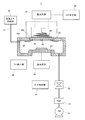
図1はICP処理装置の概略構成図である。ICP処理装置1は、金属又は金属酸化物から成るサンプル10を収納する気密な処理室20を有する。処理室20の上部には処理ガス通路21が接続されており、これを通じて処理ガス供給部22からプラズマエッチング処理用のガスが処理室20内部へ供給される。処理室20内部の圧力は、ロータリポンプ31、ターボ分子ポンプ32、弁33及び圧力制御器34を含む圧力制御機構により低圧に制御される。
FIG. 1 is a schematic configuration diagram of an ICP processing apparatus. The
処理室20の底部には、サンプル10を載置するための下部電極23が備えられている。下部電極23は第一の整合回路35を介して第一の高周波(RF)発生器36に接続されている。第一のRF発生器36は、処理室20内に発生するプラズマイオンをサンプル10へ向けて加速するためのバイアス電圧を下部電極23に印加する。
A
処理室20の上壁面(天井)201には開口を有する円形の窓材受け部202が設けられており、ここに誘電体から成る円板状の窓材25が配置されている。窓材25の内面は捨て板27(図2(B)参照)により隠蔽されており、更にその捨て板27の下面にマスク部材50が装着されている。この捨て板27と窓材25とを合わせた全体が本発明の誘電体窓に相当する。一方、窓材25の上面には渦巻き状のコイル電極26が配置されている。コイル電極26は第二の整合回路37を介して第二のRF発生器38に接続されている。第二のRF発生器38は、高周波磁界をコイル電極26から発生させるための高周波電圧をコイル電極26に印加する。
A circular window
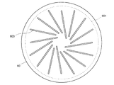
マスク部材50の構造を図2に示す。図2において、(A)は処理室20内から見たマスク部材50を示し、(B)は(A)のIIB−IIB線におけるマスク部材50の断面を示す。マスク部材50は処理室20の窓材受け部202に形成された円形の開口203内に配置され、ネジ51により天井201に固定されたリング状のマスク支持部品52により、捨て板27の下に支持されている。マスク部材50の上面には円周に沿って段部501が形成されており、これにより捨て板27とマスク部材50との間に隙間502が形成されている。また、マスク部材50の段部501より内側には32本の直線状のスリットが形成されている。
The structure of the
スリットは、マスク部材50の直径の約1/7の長さ寸法の短スリット503と、約1/3の長さ寸法の長スリット504から成り、これら短スリット503と長スリット504が周方向に交互に配置されている。
短スリット503はマスク部材50の外周側に寄せて配置されている。また、長スリット504はマスク部材50の中心と外周縁との間の中間部分に配置されており、それら長スリット504の4本のうちの1本はマスク部材50のやや中心側に寄せて配置されている。
短スリット503及び長スリット504は、いずれもマスク部材50の中心から径方向に延びる直線に対して一定の角度(図2に示す例では、約10°)だけ傾いており、全体として放射渦巻状に配置されている。このような配置により、いずれの2個のスリットも同一直線上に位置することがない。従って、全てのスリット(短スリット503及び長スリット504)の両端部に発生する亀裂の方向が異なることになり、亀裂の発生を抑えることができる。また、たとえいずれかのスリットの端部に亀裂が発生しても、その亀裂が他のスリットの端部に発生した亀裂と結合し難くなるため、マスク部材50が大きく破損することを抑えることができる。
The slit includes a
The
Each of the
図3は本発明の実施例2のマスク部材を示す図である。このマスク部材60は、段部601より内側に、該マスク部材60の中心から外へ放射渦巻状に配置された16個のスリット603を有する。各スリット603は全て同じ長さであり、マスク部材60の直径の約1/3の長さを有している。このようなマスク部材60を用いても、上記マスク部材50で得られたのと同様の効果が得られる。
FIG. 3 is a view showing a mask member according to Embodiment 2 of the present invention. The
図4は本発明の実施例3に係るマスク部材を示す図である。このマスク部材70は、段部701よりも内側に、該マスク部材70の中心から放射状に配置された9個のスリット703を有する。これらスリット703は、図4に一点鎖線で示す正九角形705の各頂点とマスク部材70の中心を結ぶ線上に位置しており、いずれの2個のスリット703も同一直線上に位置しないようになっている。このようなマスク部材70を用いても、上記マスク部材50で得られたのと同様の効果が得られる。
FIG. 4 is a view showing a mask member according to Embodiment 3 of the present invention. The mask member 70 has nine
なお、ここでは、正九角形705の各頂点とマスク部材70の中心を結ぶ線上にスリット703を設けた例を示したが、n角形(nは奇数)の各頂点とマスク部材の中心を結ぶ線上にスリットを設ければ、いずれの2個のスリットも同一直線上に位置しないため、上記マスク部材70と同様の効果が得られる。
Here, an example in which the
さらに、上記した各実施例では円板状のマスク部材を例に挙げて説明したが、本発明は円板状以外の例えば矩形板状のマスク部材にも適用できる等、要旨を逸脱しない範囲で種々の変形が可能である。 Further, in each of the above-described embodiments, the disk-shaped mask member has been described as an example. However, the present invention can be applied to, for example, a rectangular plate-shaped mask member other than the disk-shaped mask member. Various modifications are possible.
1…誘導結合形プラズマ処理装置(ICP処理装置)
10…サンプル(加工対象物)
20…処理室
23…下部電極
25…窓材
26…コイル電極
36、38…高周波(RF)発生器
50、60、70…マスク部材
503、504、603、703…スリット
1. Inductively coupled plasma processing apparatus (ICP processing apparatus)
10 ... Sample (object to be processed)
20 ... Processing
Claims (2)
プラズマ処理中に前記加工対象物から飛散した金属原子が前記誘導体窓の前記面に付着することにより該面上に形成される導電性膜が、前記コイル電極の発生する高周波磁界の作用により該導電性膜内に誘起される電流の流れを途中で遮断するような形状となるように、前記誘電体窓の一部にのみ前記金属原子を付着させるための複数の直線状のスリットを有し、
前記複数の直線状のスリットが、放射渦巻状に配置されており、いずれのスリットも他のスリットと同一の直線上に位置しないことを特徴とする誘導結合形プラズマ処理装置のマスク部材。 A processing chamber in which an object to be processed containing metal atoms is stored, a plate-shaped dielectric window provided in the processing chamber for introducing high-frequency power into the processing chamber, and disposed behind the dielectric window. A mask member mounted on a surface of the dielectric window facing the processing chamber of the inductively coupled plasma processing apparatus including the coil electrode,
A conductive film formed on the surface of the dielectric window due to metal atoms scattered from the workpiece during plasma processing adheres to the conductive film by the action of a high-frequency magnetic field generated by the coil electrode. A plurality of linear slits for adhering the metal atoms only to a part of the dielectric window so as to be a shape that interrupts the flow of current induced in the conductive film halfway,
The mask member of an inductively coupled plasma processing apparatus, wherein the plurality of linear slits are arranged in a radial spiral shape, and none of the slits is positioned on the same straight line as other slits.
プラズマ処理中に前記加工対象物から飛散した金属原子が前記誘導体窓の前記面に付着することにより該面上に形成される導電性膜が、前記コイル電極の発生する高周波磁界の作用により該導電性膜内に誘起される電流の流れを途中で遮断するような形状となるように、前記誘電体窓の一部にのみ前記金属原子を付着させるための複数の直線状のスリットを有し、
前記複数の直線状のスリットが、n角形(nは奇数)の中心から頂点に向かって延びる直線上に位置するn個の直線状のスリットから構成されており いずれのスリットも他のスリットと同一の直線上に位置しないことを特徴とする誘導結合形プラズマ処理装置のマスク部材。 A processing chamber in which an object to be processed containing metal atoms is stored, a plate-shaped dielectric window provided in the processing chamber for introducing high-frequency power into the processing chamber, and disposed behind the dielectric window. A mask member mounted on a surface of the dielectric window facing the processing chamber of the inductively coupled plasma processing apparatus including the coil electrode,
A conductive film formed on the surface of the dielectric window due to metal atoms scattered from the workpiece during plasma processing adheres to the conductive film by the action of a high-frequency magnetic field generated by the coil electrode. A plurality of linear slits for adhering the metal atoms only to a part of the dielectric window so as to be a shape that interrupts the flow of current induced in the conductive film halfway,
The plurality of linear slits are composed of n linear slits located on a straight line extending from the center of the n-gon (n is an odd number) toward the apex, and each slit is the same as the other slits. A mask member for an inductively coupled plasma processing apparatus, wherein the mask member is not located on a straight line.
Priority Applications (1)
| Application Number | Priority Date | Filing Date | Title |
|---|---|---|---|
| JP2011281886A JP5822133B2 (en) | 2011-12-22 | 2011-12-22 | Mask member of inductively coupled plasma processing apparatus |
Applications Claiming Priority (1)
| Application Number | Priority Date | Filing Date | Title |
|---|---|---|---|
| JP2011281886A JP5822133B2 (en) | 2011-12-22 | 2011-12-22 | Mask member of inductively coupled plasma processing apparatus |
Publications (3)
| Publication Number | Publication Date |
|---|---|
| JP2013129897A JP2013129897A (en) | 2013-07-04 |
| JP2013129897A5 JP2013129897A5 (en) | 2014-10-16 |
| JP5822133B2 true JP5822133B2 (en) | 2015-11-24 |
Family
ID=48907683
Family Applications (1)
| Application Number | Title | Priority Date | Filing Date |
|---|---|---|---|
| JP2011281886A Active JP5822133B2 (en) | 2011-12-22 | 2011-12-22 | Mask member of inductively coupled plasma processing apparatus |
Country Status (1)
| Country | Link |
|---|---|
| JP (1) | JP5822133B2 (en) |
Families Citing this family (2)
| Publication number | Priority date | Publication date | Assignee | Title |
|---|---|---|---|---|
| CN107393790A (en) * | 2017-07-20 | 2017-11-24 | 中国科学院电子学研究所 | The method for metallising of electron tube dielectric disk in window |
| JP7469625B2 (en) * | 2020-04-13 | 2024-04-17 | 日新電機株式会社 | Plasma source and plasma processing device |
Family Cites Families (7)
| Publication number | Priority date | Publication date | Assignee | Title |
|---|---|---|---|---|
| JPH01184922A (en) * | 1988-01-20 | 1989-07-24 | Canon Inc | Plasma processor useful for etching, ashing, film formation and the like |
| JP3364675B2 (en) * | 1997-09-30 | 2003-01-08 | 東京エレクトロンエイ・ティー株式会社 | Plasma processing equipment |
| JP4119547B2 (en) * | 1997-10-20 | 2008-07-16 | 東京エレクトロンAt株式会社 | Plasma processing equipment |
| JP4193255B2 (en) * | 1998-12-01 | 2008-12-10 | 株式会社日立製作所 | Plasma processing apparatus and plasma processing method |
| JP4469054B2 (en) * | 2000-03-10 | 2010-05-26 | サムコ株式会社 | Inductively coupled plasma processing equipment |
| JP2008133538A (en) * | 2006-10-27 | 2008-06-12 | Mitsubishi Materials Corp | Method of separating and recovering target waste material and indium |
| JP4888076B2 (en) * | 2006-11-17 | 2012-02-29 | パナソニック株式会社 | Plasma etching equipment |
-
2011
- 2011-12-22 JP JP2011281886A patent/JP5822133B2/en active Active
Also Published As
| Publication number | Publication date |
|---|---|
| JP2013129897A (en) | 2013-07-04 |
Similar Documents
| Publication | Publication Date | Title |
|---|---|---|
| KR102434088B1 (en) | Plasma processing apparatus and plasma processing method | |
| JP5380464B2 (en) | Plasma processing apparatus, plasma processing method, and method of manufacturing element including substrate to be processed | |
| JP5561812B2 (en) | Plasma processing equipment | |
| JP6284825B2 (en) | Plasma processing equipment | |
| JP5286351B2 (en) | Magnetron sputtering apparatus and magnetron sputtering method | |
| EP3648553B1 (en) | Plasma treatment device | |
| TWI695079B (en) | Method and apparatus for depositing a material | |
| KR20160011564A (en) | Plasma processing apparatus and plasma processing method | |
| JP2006511945A (en) | Method and apparatus for enhancing and localizing capacitively coupled plasma and magnet assembly | |
| TWI548766B (en) | Sputtering device | |
| JP2016511911A (en) | Plasma chemical vapor deposition (PECVD) source | |
| JP5822133B2 (en) | Mask member of inductively coupled plasma processing apparatus | |
| JP5231962B2 (en) | Sheet plasma deposition system | |
| JP7102260B2 (en) | Opposed target type sputtering film deposition equipment | |
| JP2012109377A (en) | Electrode structure and plasma processing apparatus | |
| JP2011034705A (en) | Plasma treatment device | |
| JP6511813B2 (en) | Plasma treated electrode and CVD electrode | |
| JP2013229150A (en) | Plasma processing apparatus | |
| JP5650281B2 (en) | Plasma processing method and plasma processing apparatus | |
| JP6462072B2 (en) | Plasma processing apparatus and plasma processing method | |
| JP6863608B2 (en) | Plasma source and plasma processing equipment | |
| JP2018029119A (en) | Inductive coupling type plasma processing device | |
| KR101533688B1 (en) | Capacitively coupled plasma chamber having reversed and non-reversed power supply | |
| JP2017218605A (en) | Film deposition apparatus | |
| JP2010031383A (en) | Plasma-assisted sputter deposition system |
Legal Events
| Date | Code | Title | Description |
|---|---|---|---|
| A521 | Request for written amendment filed |
Free format text: JAPANESE INTERMEDIATE CODE: A523 Effective date: 20140829 |
|
| A621 | Written request for application examination |
Free format text: JAPANESE INTERMEDIATE CODE: A621 Effective date: 20140829 |
|
| A977 | Report on retrieval |
Free format text: JAPANESE INTERMEDIATE CODE: A971007 Effective date: 20150528 |
|
| A131 | Notification of reasons for refusal |
Free format text: JAPANESE INTERMEDIATE CODE: A131 Effective date: 20150602 |
|
| A521 | Request for written amendment filed |
Free format text: JAPANESE INTERMEDIATE CODE: A523 Effective date: 20150728 |
|
| TRDD | Decision of grant or rejection written | ||
| A01 | Written decision to grant a patent or to grant a registration (utility model) |
Free format text: JAPANESE INTERMEDIATE CODE: A01 Effective date: 20150825 |
|
| A61 | First payment of annual fees (during grant procedure) |
Free format text: JAPANESE INTERMEDIATE CODE: A61 Effective date: 20150924 |
|
| R150 | Certificate of patent or registration of utility model |
Ref document number: 5822133 Country of ref document: JP Free format text: JAPANESE INTERMEDIATE CODE: R150 |
|
| R250 | Receipt of annual fees |
Free format text: JAPANESE INTERMEDIATE CODE: R250 |
|
| R250 | Receipt of annual fees |
Free format text: JAPANESE INTERMEDIATE CODE: R250 |
|
| R250 | Receipt of annual fees |
Free format text: JAPANESE INTERMEDIATE CODE: R250 |
|
| R250 | Receipt of annual fees |
Free format text: JAPANESE INTERMEDIATE CODE: R250 |
|
| R250 | Receipt of annual fees |
Free format text: JAPANESE INTERMEDIATE CODE: R250 |
|
| R250 | Receipt of annual fees |
Free format text: JAPANESE INTERMEDIATE CODE: R250 |