JP5814654B2 - Silicon substrate processing method and liquid discharge head manufacturing method - Google Patents
Silicon substrate processing method and liquid discharge head manufacturing method Download PDFInfo
- Publication number
- JP5814654B2 JP5814654B2 JP2011140644A JP2011140644A JP5814654B2 JP 5814654 B2 JP5814654 B2 JP 5814654B2 JP 2011140644 A JP2011140644 A JP 2011140644A JP 2011140644 A JP2011140644 A JP 2011140644A JP 5814654 B2 JP5814654 B2 JP 5814654B2
- Authority
- JP
- Japan
- Prior art keywords
- silicon substrate
- recess
- opening
- etching
- liquid chamber
- Prior art date
- Legal status (The legal status is an assumption and is not a legal conclusion. Google has not performed a legal analysis and makes no representation as to the accuracy of the status listed.)
- Expired - Fee Related
Links
- 239000000758 substrate Substances 0.000 title claims description 229
- 239000007788 liquid Substances 0.000 title claims description 217
- 229910052710 silicon Inorganic materials 0.000 title claims description 162
- 239000010703 silicon Substances 0.000 title claims description 162
- XUIMIQQOPSSXEZ-UHFFFAOYSA-N Silicon Chemical compound [Si] XUIMIQQOPSSXEZ-UHFFFAOYSA-N 0.000 title claims description 161
- 238000003672 processing method Methods 0.000 title claims description 18
- 238000004519 manufacturing process Methods 0.000 title claims description 13
- 238000005530 etching Methods 0.000 claims description 129
- 238000000034 method Methods 0.000 claims description 84
- 238000000059 patterning Methods 0.000 claims description 24
- 238000009623 Bosch process Methods 0.000 claims description 19
- 238000001020 plasma etching Methods 0.000 claims description 16
- 239000013078 crystal Substances 0.000 claims description 15
- 238000000206 photolithography Methods 0.000 claims description 3
- 230000001678 irradiating effect Effects 0.000 claims description 2
- 238000003754 machining Methods 0.000 claims 1
- 239000010408 film Substances 0.000 description 94
- 239000010410 layer Substances 0.000 description 68
- 239000011347 resin Substances 0.000 description 31
- 229920005989 resin Polymers 0.000 description 31
- 238000001312 dry etching Methods 0.000 description 28
- VYPSYNLAJGMNEJ-UHFFFAOYSA-N Silicium dioxide Chemical compound O=[Si]=O VYPSYNLAJGMNEJ-UHFFFAOYSA-N 0.000 description 23
- 239000000463 material Substances 0.000 description 23
- 229910052814 silicon oxide Inorganic materials 0.000 description 23
- 230000008569 process Effects 0.000 description 22
- 150000002500 ions Chemical class 0.000 description 18
- 230000000694 effects Effects 0.000 description 17
- KRHYYFGTRYWZRS-UHFFFAOYSA-N Fluorane Chemical compound F KRHYYFGTRYWZRS-UHFFFAOYSA-N 0.000 description 16
- 238000000465 moulding Methods 0.000 description 15
- 230000002940 repellent Effects 0.000 description 14
- 239000005871 repellent Substances 0.000 description 14
- 238000000151 deposition Methods 0.000 description 11
- 230000008021 deposition Effects 0.000 description 11
- 238000010586 diagram Methods 0.000 description 11
- 239000007789 gas Substances 0.000 description 9
- 239000000243 solution Substances 0.000 description 9
- 239000011241 protective layer Substances 0.000 description 8
- WGTYBPLFGIVFAS-UHFFFAOYSA-M tetramethylammonium hydroxide Chemical compound [OH-].C[N+](C)(C)C WGTYBPLFGIVFAS-UHFFFAOYSA-M 0.000 description 8
- 229910052581 Si3N4 Inorganic materials 0.000 description 7
- PCHJSUWPFVWCPO-UHFFFAOYSA-N gold Chemical compound [Au] PCHJSUWPFVWCPO-UHFFFAOYSA-N 0.000 description 7
- 229910052737 gold Inorganic materials 0.000 description 7
- 239000010931 gold Substances 0.000 description 7
- HQVNEWCFYHHQES-UHFFFAOYSA-N silicon nitride Chemical compound N12[Si]34N5[Si]62N3[Si]51N64 HQVNEWCFYHHQES-UHFFFAOYSA-N 0.000 description 7
- 238000005507 spraying Methods 0.000 description 7
- 238000005498 polishing Methods 0.000 description 6
- 229920002614 Polyether block amide Polymers 0.000 description 5
- 230000015572 biosynthetic process Effects 0.000 description 5
- 238000001039 wet etching Methods 0.000 description 5
- CDBYLPFSWZWCQE-UHFFFAOYSA-L Sodium Carbonate Chemical compound [Na+].[Na+].[O-]C([O-])=O CDBYLPFSWZWCQE-UHFFFAOYSA-L 0.000 description 4
- PNEYBMLMFCGWSK-UHFFFAOYSA-N aluminium oxide Inorganic materials [O-2].[O-2].[O-2].[Al+3].[Al+3] PNEYBMLMFCGWSK-UHFFFAOYSA-N 0.000 description 4
- 230000018109 developmental process Effects 0.000 description 4
- 230000004927 fusion Effects 0.000 description 4
- 230000005865 ionizing radiation Effects 0.000 description 4
- 229910044991 metal oxide Inorganic materials 0.000 description 4
- 150000004706 metal oxides Chemical class 0.000 description 4
- 239000000126 substance Substances 0.000 description 4
- LPEKGGXMPWTOCB-UHFFFAOYSA-N 8beta-(2,3-epoxy-2-methylbutyryloxy)-14-acetoxytithifolin Natural products COC(=O)C(C)O LPEKGGXMPWTOCB-UHFFFAOYSA-N 0.000 description 3
- RYGMFSIKBFXOCR-UHFFFAOYSA-N Copper Chemical compound [Cu] RYGMFSIKBFXOCR-UHFFFAOYSA-N 0.000 description 3
- CTQNGGLPUBDAKN-UHFFFAOYSA-N O-Xylene Chemical compound CC1=CC=CC=C1C CTQNGGLPUBDAKN-UHFFFAOYSA-N 0.000 description 3
- 239000000853 adhesive Substances 0.000 description 3
- 230000001070 adhesive effect Effects 0.000 description 3
- 229910052782 aluminium Inorganic materials 0.000 description 3
- XAGFODPZIPBFFR-UHFFFAOYSA-N aluminium Chemical compound [Al] XAGFODPZIPBFFR-UHFFFAOYSA-N 0.000 description 3
- 239000007864 aqueous solution Substances 0.000 description 3
- 229910052802 copper Inorganic materials 0.000 description 3
- 239000010949 copper Substances 0.000 description 3
- 238000009792 diffusion process Methods 0.000 description 3
- 238000007599 discharging Methods 0.000 description 3
- ODQWQRRAPPTVAG-GZTJUZNOSA-N doxepin Chemical compound C1OC2=CC=CC=C2C(=C/CCN(C)C)/C2=CC=CC=C21 ODQWQRRAPPTVAG-GZTJUZNOSA-N 0.000 description 3
- 230000005496 eutectics Effects 0.000 description 3
- 238000000227 grinding Methods 0.000 description 3
- 238000010438 heat treatment Methods 0.000 description 3
- 125000002887 hydroxy group Chemical group [H]O* 0.000 description 3
- 238000007654 immersion Methods 0.000 description 3
- 229940057867 methyl lactate Drugs 0.000 description 3
- 230000003647 oxidation Effects 0.000 description 3
- 238000007254 oxidation reaction Methods 0.000 description 3
- HBMJWWWQQXIZIP-UHFFFAOYSA-N silicon carbide Chemical compound [Si+]#[C-] HBMJWWWQQXIZIP-UHFFFAOYSA-N 0.000 description 3
- 239000007921 spray Substances 0.000 description 3
- 239000008096 xylene Substances 0.000 description 3
- 239000004925 Acrylic resin Substances 0.000 description 2
- 229920000178 Acrylic resin Polymers 0.000 description 2
- KDLHZDBZIXYQEI-UHFFFAOYSA-N Palladium Chemical compound [Pd] KDLHZDBZIXYQEI-UHFFFAOYSA-N 0.000 description 2
- NBIIXXVUZAFLBC-UHFFFAOYSA-N Phosphoric acid Chemical compound OP(O)(O)=O NBIIXXVUZAFLBC-UHFFFAOYSA-N 0.000 description 2
- 206010034972 Photosensitivity reaction Diseases 0.000 description 2
- ATJFFYVFTNAWJD-UHFFFAOYSA-N Tin Chemical compound [Sn] ATJFFYVFTNAWJD-UHFFFAOYSA-N 0.000 description 2
- 239000012298 atmosphere Substances 0.000 description 2
- QVGXLLKOCUKJST-UHFFFAOYSA-N atomic oxygen Chemical compound [O] QVGXLLKOCUKJST-UHFFFAOYSA-N 0.000 description 2
- UMIVXZPTRXBADB-UHFFFAOYSA-N benzocyclobutene Chemical compound C1=CC=C2CCC2=C1 UMIVXZPTRXBADB-UHFFFAOYSA-N 0.000 description 2
- 238000006243 chemical reaction Methods 0.000 description 2
- 238000000576 coating method Methods 0.000 description 2
- 239000004205 dimethyl polysiloxane Substances 0.000 description 2
- 239000012776 electronic material Substances 0.000 description 2
- 239000003822 epoxy resin Substances 0.000 description 2
- NBVXSUQYWXRMNV-UHFFFAOYSA-N fluoromethane Chemical compound FC NBVXSUQYWXRMNV-UHFFFAOYSA-N 0.000 description 2
- 239000001257 hydrogen Substances 0.000 description 2
- 229910052739 hydrogen Inorganic materials 0.000 description 2
- 229910052751 metal Inorganic materials 0.000 description 2
- 239000002184 metal Substances 0.000 description 2
- 239000007769 metal material Substances 0.000 description 2
- QVEIBLDXZNGPHR-UHFFFAOYSA-N naphthalene-1,4-dione;diazide Chemical class [N-]=[N+]=[N-].[N-]=[N+]=[N-].C1=CC=C2C(=O)C=CC(=O)C2=C1 QVEIBLDXZNGPHR-UHFFFAOYSA-N 0.000 description 2
- 229920003986 novolac Polymers 0.000 description 2
- 239000001301 oxygen Substances 0.000 description 2
- 229910052760 oxygen Inorganic materials 0.000 description 2
- 229920002120 photoresistant polymer Polymers 0.000 description 2
- 230000036211 photosensitivity Effects 0.000 description 2
- 238000009832 plasma treatment Methods 0.000 description 2
- 229920000435 poly(dimethylsiloxane) Polymers 0.000 description 2
- 229920003229 poly(methyl methacrylate) Polymers 0.000 description 2
- 229920000647 polyepoxide Polymers 0.000 description 2
- 239000004926 polymethyl methacrylate Substances 0.000 description 2
- 238000007639 printing Methods 0.000 description 2
- 230000001681 protective effect Effects 0.000 description 2
- 239000004065 semiconductor Substances 0.000 description 2
- 229910010271 silicon carbide Inorganic materials 0.000 description 2
- 229910000029 sodium carbonate Inorganic materials 0.000 description 2
- 230000003746 surface roughness Effects 0.000 description 2
- 229910052718 tin Inorganic materials 0.000 description 2
- 239000011135 tin Substances 0.000 description 2
- OIICUUGPVAEJSH-UHFFFAOYSA-M (2-bromophenyl)methyl-ethyl-dimethylazanium;bromide Chemical compound [Br-].CC[N+](C)(C)CC1=CC=CC=C1Br OIICUUGPVAEJSH-UHFFFAOYSA-M 0.000 description 1
- VYZAMTAEIAYCRO-UHFFFAOYSA-N Chromium Chemical compound [Cr] VYZAMTAEIAYCRO-UHFFFAOYSA-N 0.000 description 1
- YCKRFDGAMUMZLT-UHFFFAOYSA-N Fluorine atom Chemical compound [F] YCKRFDGAMUMZLT-UHFFFAOYSA-N 0.000 description 1
- 229910000147 aluminium phosphate Inorganic materials 0.000 description 1
- 238000000137 annealing Methods 0.000 description 1
- 238000004380 ashing Methods 0.000 description 1
- 230000008901 benefit Effects 0.000 description 1
- 229910052804 chromium Inorganic materials 0.000 description 1
- 239000011651 chromium Substances 0.000 description 1
- 239000011248 coating agent Substances 0.000 description 1
- 238000000354 decomposition reaction Methods 0.000 description 1
- 238000006297 dehydration reaction Methods 0.000 description 1
- 238000003618 dip coating Methods 0.000 description 1
- 238000007598 dipping method Methods 0.000 description 1
- 238000010018 discharge printing Methods 0.000 description 1
- 239000011737 fluorine Substances 0.000 description 1
- 229910052731 fluorine Inorganic materials 0.000 description 1
- 229910052732 germanium Inorganic materials 0.000 description 1
- GNPVGFCGXDBREM-UHFFFAOYSA-N germanium atom Chemical compound [Ge] GNPVGFCGXDBREM-UHFFFAOYSA-N 0.000 description 1
- 230000009477 glass transition Effects 0.000 description 1
- LNEPOXFFQSENCJ-UHFFFAOYSA-N haloperidol Chemical compound C1CC(O)(C=2C=CC(Cl)=CC=2)CCN1CCCC(=O)C1=CC=C(F)C=C1 LNEPOXFFQSENCJ-UHFFFAOYSA-N 0.000 description 1
- 230000006872 improvement Effects 0.000 description 1
- 229910052738 indium Inorganic materials 0.000 description 1
- APFVFJFRJDLVQX-UHFFFAOYSA-N indium atom Chemical compound [In] APFVFJFRJDLVQX-UHFFFAOYSA-N 0.000 description 1
- 238000005304 joining Methods 0.000 description 1
- 238000001459 lithography Methods 0.000 description 1
- 230000007246 mechanism Effects 0.000 description 1
- 230000001404 mediated effect Effects 0.000 description 1
- 150000002739 metals Chemical class 0.000 description 1
- 239000003595 mist Substances 0.000 description 1
- 239000000203 mixture Substances 0.000 description 1
- 125000004430 oxygen atom Chemical group O* 0.000 description 1
- 229910052763 palladium Inorganic materials 0.000 description 1
- 238000005268 plasma chemical vapour deposition Methods 0.000 description 1
- -1 polydimethylsiloxane Polymers 0.000 description 1
- 229920001721 polyimide Polymers 0.000 description 1
- 239000009719 polyimide resin Substances 0.000 description 1
- 238000011176 pooling Methods 0.000 description 1
- 238000002360 preparation method Methods 0.000 description 1
- 230000009257 reactivity Effects 0.000 description 1
- 230000009467 reduction Effects 0.000 description 1
- 230000007261 regionalization Effects 0.000 description 1
- 150000003376 silicon Chemical class 0.000 description 1
- LIVNPJMFVYWSIS-UHFFFAOYSA-N silicon monoxide Chemical compound [Si-]#[O+] LIVNPJMFVYWSIS-UHFFFAOYSA-N 0.000 description 1
- 239000002210 silicon-based material Substances 0.000 description 1
- 239000002904 solvent Substances 0.000 description 1
- 238000004528 spin coating Methods 0.000 description 1
- 230000001629 suppression Effects 0.000 description 1
- 239000010409 thin film Substances 0.000 description 1
Images


Classifications
-
- B—PERFORMING OPERATIONS; TRANSPORTING
- B41—PRINTING; LINING MACHINES; TYPEWRITERS; STAMPS
- B41J—TYPEWRITERS; SELECTIVE PRINTING MECHANISMS, i.e. MECHANISMS PRINTING OTHERWISE THAN FROM A FORME; CORRECTION OF TYPOGRAPHICAL ERRORS
- B41J2/00—Typewriters or selective printing mechanisms characterised by the printing or marking process for which they are designed
- B41J2/005—Typewriters or selective printing mechanisms characterised by the printing or marking process for which they are designed characterised by bringing liquid or particles selectively into contact with a printing material
- B41J2/01—Ink jet
- B41J2/135—Nozzles
- B41J2/16—Production of nozzles
- B41J2/1601—Production of bubble jet print heads
- B41J2/1603—Production of bubble jet print heads of the front shooter type
-
- B—PERFORMING OPERATIONS; TRANSPORTING
- B41—PRINTING; LINING MACHINES; TYPEWRITERS; STAMPS
- B41J—TYPEWRITERS; SELECTIVE PRINTING MECHANISMS, i.e. MECHANISMS PRINTING OTHERWISE THAN FROM A FORME; CORRECTION OF TYPOGRAPHICAL ERRORS
- B41J2/00—Typewriters or selective printing mechanisms characterised by the printing or marking process for which they are designed
- B41J2/005—Typewriters or selective printing mechanisms characterised by the printing or marking process for which they are designed characterised by bringing liquid or particles selectively into contact with a printing material
- B41J2/01—Ink jet
- B41J2/135—Nozzles
- B41J2/16—Production of nozzles
- B41J2/1621—Manufacturing processes
- B41J2/1626—Manufacturing processes etching
- B41J2/1629—Manufacturing processes etching wet etching
-
- B—PERFORMING OPERATIONS; TRANSPORTING
- B41—PRINTING; LINING MACHINES; TYPEWRITERS; STAMPS
- B41J—TYPEWRITERS; SELECTIVE PRINTING MECHANISMS, i.e. MECHANISMS PRINTING OTHERWISE THAN FROM A FORME; CORRECTION OF TYPOGRAPHICAL ERRORS
- B41J2/00—Typewriters or selective printing mechanisms characterised by the printing or marking process for which they are designed
- B41J2/005—Typewriters or selective printing mechanisms characterised by the printing or marking process for which they are designed characterised by bringing liquid or particles selectively into contact with a printing material
- B41J2/01—Ink jet
- B41J2/135—Nozzles
- B41J2/16—Production of nozzles
- B41J2/1621—Manufacturing processes
- B41J2/1631—Manufacturing processes photolithography
-
- B—PERFORMING OPERATIONS; TRANSPORTING
- B41—PRINTING; LINING MACHINES; TYPEWRITERS; STAMPS
- B41J—TYPEWRITERS; SELECTIVE PRINTING MECHANISMS, i.e. MECHANISMS PRINTING OTHERWISE THAN FROM A FORME; CORRECTION OF TYPOGRAPHICAL ERRORS
- B41J2/00—Typewriters or selective printing mechanisms characterised by the printing or marking process for which they are designed
- B41J2/005—Typewriters or selective printing mechanisms characterised by the printing or marking process for which they are designed characterised by bringing liquid or particles selectively into contact with a printing material
- B41J2/01—Ink jet
- B41J2/135—Nozzles
- B41J2/14—Structure thereof only for on-demand ink jet heads
- B41J2002/14467—Multiple feed channels per ink chamber
-
- H—ELECTRICITY
- H01—ELECTRIC ELEMENTS
- H01L—SEMICONDUCTOR DEVICES NOT COVERED BY CLASS H10
- H01L21/00—Processes or apparatus adapted for the manufacture or treatment of semiconductor or solid state devices or of parts thereof
- H01L21/02—Manufacture or treatment of semiconductor devices or of parts thereof
- H01L21/04—Manufacture or treatment of semiconductor devices or of parts thereof the devices having at least one potential-jump barrier or surface barrier, e.g. PN junction, depletion layer or carrier concentration layer
- H01L21/18—Manufacture or treatment of semiconductor devices or of parts thereof the devices having at least one potential-jump barrier or surface barrier, e.g. PN junction, depletion layer or carrier concentration layer the devices having semiconductor bodies comprising elements of Group IV of the Periodic System or AIIIBV compounds with or without impurities, e.g. doping materials
- H01L21/30—Treatment of semiconductor bodies using processes or apparatus not provided for in groups H01L21/20 - H01L21/26
- H01L21/302—Treatment of semiconductor bodies using processes or apparatus not provided for in groups H01L21/20 - H01L21/26 to change their surface-physical characteristics or shape, e.g. etching, polishing, cutting
- H01L21/306—Chemical or electrical treatment, e.g. electrolytic etching
- H01L21/3065—Plasma etching; Reactive-ion etching
- H01L21/30655—Plasma etching; Reactive-ion etching comprising alternated and repeated etching and passivation steps, e.g. Bosch process
Description
本発明は、シリコン基板の加工方法に関する。より好ましくは、液体吐出ヘッドを製造するために用いるシリコン基板の加工方法に関する。 The present invention relates to a method for processing a silicon substrate. More preferably, the present invention relates to a method for processing a silicon substrate used for manufacturing a liquid discharge head.
現在、半導体デバイスの微細加工技術を応用して、液体吐出ヘッド用のシリコン基板の加工が行われている。また、近年の液体吐出記録装置においては、高解像度、高速印字といった印字性能の向上が求められている。そのため、吐出液滴のより正確な着弾と高速な液体のリフィルを実現することが求められている。 Currently, processing of a silicon substrate for a liquid discharge head is performed by applying a fine processing technique of a semiconductor device. In recent liquid discharge recording apparatuses, improvement in printing performance such as high resolution and high speed printing is required. Therefore, it is required to realize more accurate landing of ejected droplets and high-speed liquid refill.
液体吐出プリント方式に用いられる一般的な液体吐出ヘッドは、特許文献1に記載されるように、シリコン基板上に、液滴を吐出するための微細な吐出口と、該吐出口に連通する液体流路と、該液体流路の一部に設けられる吐出エネルギー発生部と、を備える。また、シリコン基板には液体流路と連通する共通液室が形成されている。
As described in
これに対して、特許文献2に記載されるような液体吐出ヘッドが開発されている。この特許文献2に記載される液体吐出ヘッドにおいては、一つの吐出口に連通する液体流路が該吐出口に対して対称に配置されている。このような構成とすることにより、発生した気泡が左右の液体流路で均等に成長するため、吐出口から飛翔する液滴の方向を安定的に垂直とすることができ、正確に着弾させることができる。 On the other hand, a liquid discharge head as described in Patent Document 2 has been developed. In the liquid discharge head described in Patent Document 2, a liquid flow path communicating with one discharge port is disposed symmetrically with respect to the discharge port. With this configuration, the generated bubbles grow evenly in the left and right liquid flow paths, so that the direction of the liquid droplets flying from the discharge port can be stably vertical and landed accurately. Can do.
上述のような液体吐出ヘッド、つまり一つの共通液室から複数の供給口が形成されたシリコン基板の形成方法として、特許文献3に記載されるように、シリコン基板に対して2段階エッチング処理を行う方法が挙げられる。特許文献3に記載の方法では、まず、結晶異方性エッチングにより第1のエッチングを行って凹部を形成して共通液室を形成する。次に、ドライエッチングにより凹部の底面に対して第2のエッチングを行うことにより、複数の供給口を形成する。このようにして、凹部からなる共通液室に連通する複数の供給口を有するシリコン基板が形成されている。
As described in
液体吐出ヘッドに用いる供給口の形成方法の一つとして、ドライエッチングが挙げられ、特にボッシュプロセスを用いたドライエッチングが望ましい。ボッシュプロセスを用いたドライエッチングは、デポ膜の形成工程、イオンによる側面以外のデポ膜の除去工程、ラジカルによるエッチング工程、を繰り返し行うことでシリコン基板を垂直形状にエッチングする技術である。しかし、凹部の底面をドライエッチングして供給口を形成する際、凹部の側壁近傍の供給口が、凹部の側壁方向に向かって傾斜してエッチングされるという現象が生じる。これは、プラズマモールディング効果と呼ばれている現象に起因する。通常、プラズマを用いてエッチングを行う場合、基板表面を等電位面として、プラズマシース(あるいは単にシース)と呼ばれる領域が形成される。このシースにはプラズマを基準として負の電位差が生じるため、シースを介してプラズマ中から基板に向かってイオンが加速される。従って、イオンはシースの等電位面に対して垂直に、即ち基板に向かって垂直に加速される。しかし、基板表面に大きな凹部が存在する場合、図8(a)に示すようにシース801は基板802の凹凸に沿って形成される。正イオンは、シースの等電位面に対して垂直に加速されるため、イオンの飛跡は凹部の側壁に向かって曲げられることになる。この現象を、供給口エッチングに適用して考える。「側壁以外のデポ物除去」は前記シースによって加速されたイオンによって行われる。従って、凹部の側壁の近傍ではデポ膜を除去するイオンが影響を受け、所望の位置よりずれた位置のデポ膜が除去されてしまう。このように、凹部を有する基板底面ではデポ膜の除去位置が連続的にずれてしまうため、ラジカルによるエッチングも連続的にずれて形成することになる。その結果、数度の角度を持ってエッチングが進行してしまうという課題があった。このような課題はボッシュプロセスを用いた場合に限定されず、一般的な反応性イオンエッチング(RIE)のドライエッチングによる場合に共通して存在する。
One method of forming the supply port used in the liquid discharge head is dry etching, and dry etching using a Bosch process is particularly desirable. Dry etching using the Bosch process is a technique for etching a silicon substrate into a vertical shape by repeatedly performing a deposition film formation process, a deposition film removal process other than side surfaces by ions, and a radical etching process. However, when the supply port is formed by dry etching the bottom surface of the recess, a phenomenon occurs in which the supply port near the sidewall of the recess is etched while being inclined toward the sidewall of the recess. This is due to a phenomenon called the plasma molding effect. Normally, when etching is performed using plasma, a region called a plasma sheath (or simply a sheath) is formed with the substrate surface as an equipotential surface. Since a negative potential difference is generated in the sheath with reference to the plasma, ions are accelerated from the plasma toward the substrate through the sheath. Thus, ions are accelerated perpendicular to the equipotential surface of the sheath, i.e. perpendicular to the substrate. However, when a large concave portion exists on the substrate surface, the
また、数度の角度をもってエッチング進行すると、得られる供給口のエッチング開始部の開口と終了部の開口とが水平方向で位置がずれてしまい、シリコン基板の表面において、供給口の開口(エッチング終了部の開口)の位置ずれが発生してしまう。その結果、近傍の配線部がダメージを受ける場合がある。また、供給口が斜めに形成されるため、他の供給口よりも長い供給口が形成されてしまい、供給性能のバラツキが生じる場合がある。さらには、未貫通の供給口が形成されてしまう場合もある。 Further, when etching proceeds at an angle of several degrees, the opening of the etching start portion and the opening of the end portion of the obtained supply port are displaced in the horizontal direction, and the opening of the supply port (etching end) on the surface of the silicon substrate. Misalignment of the opening) occurs. As a result, nearby wiring portions may be damaged. Further, since the supply port is formed obliquely, a supply port longer than the other supply ports is formed, and the supply performance may vary. Furthermore, an unpenetrated supply port may be formed.
そこで、本発明は、ドライエッチングを用いてシリコン基板における凹部の底部から該凹部が形成されている面と相対する面に向かって垂直な開口を設けることができるシリコン基板の加工方法を提供することを目的とする。より好ましくは、ドライエッチングを用いて、シリコン基板の凹部からなる共通液室の底部を垂直にエッチングし、高い開口位置精度で複数の供給口を形成することができるシリコン基板の加工方法を提供することを目的とする。 Accordingly, the present invention provides a method for processing a silicon substrate, which can provide a vertical opening from the bottom of a recess in a silicon substrate to a surface opposite to the surface where the recess is formed by using dry etching. With the goal. More preferably, there is provided a silicon substrate processing method capable of forming a plurality of supply ports with high opening position accuracy by vertically etching a bottom portion of a common liquid chamber formed of a concave portion of a silicon substrate by using dry etching. For the purpose.
そこで、本発明は、第1の面と該第1の面と反対側の第2の面とを有するシリコン基板の加工方法であって、
(1)前記第2の面から前記第1の面側に向かって第1の凹部を形成する工程と、
(2)前記第1の凹部の底面にパターン開口を有するパターニングマスクを形成する工程と、
(3)前記第1の凹部の前記第2の面側の開口の一部を遮蔽するように、前記第2の面と平行な遮蔽構造を形成する工程と、
(4)前記第2の面側から反応性イオンエッチングを行い、第2の凹部を形成する工程と、
を有することを特徴とするシリコン基板の加工方法である。
Therefore, the present invention is a method for processing a silicon substrate having a first surface and a second surface opposite to the first surface,
(1) forming a first recess from the second surface toward the first surface;
(2) forming a patterning mask having a pattern opening on the bottom surface of the first recess;
(3) forming a shielding structure parallel to the second surface so as to shield part of the opening on the second surface side of the first recess;
(4) performing reactive ion etching from the second surface side to form a second recess;
A method for processing a silicon substrate, comprising:
本発明に係るシリコン基板の加工方法によって、第1の開口に形成する第2の開口をより垂直に形成できる。したがって、第2の開口の開口位置精度を向上でき、高い信頼性を得ることが出来る。 With the method for processing a silicon substrate according to the present invention, the second opening formed in the first opening can be formed more vertically. Therefore, the opening position accuracy of the second opening can be improved, and high reliability can be obtained.
シースが発生するメカニズムは、電子とイオンの移動度の差による。チャンバー壁や基板等、プラズマ内に境界領域が存在する場合、質量の小さい電子が先に到達して、プラズマに対して負の電位を形成される。それを遮蔽するように正電荷の多い領域が形成されバランスが保たれる。これがシースであり、境界面を等電位面として、それに平行となるように形成される。さらに、基板にバイアスパワーを印加すると、基板の負の電位は助長され、イオンを引きこむエネルギーも増加する。これを利用したものが反応性イオンエッチングである。 The mechanism by which the sheath is generated is due to the difference in mobility between electrons and ions. When a boundary region exists in the plasma, such as a chamber wall or a substrate, electrons with a small mass reach first and form a negative potential with respect to the plasma. A region with a lot of positive charges is formed so as to shield it, and the balance is maintained. This is a sheath, which is formed so that the boundary surface is an equipotential surface and is parallel thereto. Furthermore, when bias power is applied to the substrate, the negative potential of the substrate is promoted and the energy for attracting ions also increases. Reactive ion etching utilizes this.
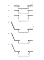
ボッシュプロセスは、上記反応性イオンエッチングの一形態である。図2(a)〜(c)に示すように、(1)CF系のデポ膜15の形成、(2)イオンによるデポ膜15の除去、(3)主にF系ラジカルによるエッチング、を連続的に繰り返すことで垂直方向へのエッチングが行われる。
The Bosch process is a form of the reactive ion etching. As shown in FIGS. 2A to 2C, (1) the formation of the CF-based
この際、(2)では、プラズマ中の+イオンがシースによって基板表面に加速されることにより、デポ膜のエッチングが進む。 At this time, in (2), + ions in the plasma are accelerated to the substrate surface by the sheath, so that etching of the deposition film proceeds.
ここで、図2(d)に示すような底面との角度が鈍角となる側面を有する凹部の底面をエッチングする場合、前述のプラズマモールディング効果により、凹部の形状に沿うようにシースが形成されてしまう。これは、シースというものが、基板表面を等電位面として、そこから一定の距離にある位置を積分して求められる等電位面を形成するからである。これにより、+イオンが基板に対して数度の角度を持って加速されることになる。その結果、側壁のデポ膜15の一部がエッチングされてしまい、(3)のエッチング時に横方向にずれてエッチングが進んでしまう場合がある。これが連続的に繰り返されることで結果的にエッチング方向は数度の角度を持って形成されることとなる(図2(d)〜(f))。
Here, when etching the bottom surface of the concave portion having a side surface with an obtuse angle with the bottom surface as shown in FIG. 2 (d), the sheath is formed along the shape of the concave portion by the plasma molding effect described above. End up. This is because the sheath forms an equipotential surface obtained by integrating the position at a certain distance from the substrate surface as the equipotential surface. As a result, + ions are accelerated at an angle of several degrees with respect to the substrate. As a result, a part of the
共通液室の底面に供給口を形成する場合を例に挙げてより具体的に説明すると、シースは共通液室の形状に沿って形成される。そして、共通液室の側面近傍に形成しようとする供給口では、共通液室の側面に形成されたシースにイオンが影響を受け、基板に対して垂直ではなく、側面の方向に数度の角度を持ってエッチングが進行してしまう場合があった。 More specifically, the case where the supply port is formed on the bottom surface of the common liquid chamber is described as an example. The sheath is formed along the shape of the common liquid chamber. At the supply port to be formed near the side surface of the common liquid chamber, ions are affected by the sheath formed on the side surface of the common liquid chamber, and the angle is several degrees in the direction of the side surface, not perpendicular to the substrate. In some cases, the etching progresses with a gap.
プラズマモールディング効果は、シースの長さと凹部の開口の寸法との相対関係によって変化し、影響が現れ始めるのはシースの長さ/凹部の開口寸法≦10程度であるという研究結果がある(D.Kim et.al.,IEEE Trans.Plasma Sci.31,691(2003))。即ち、シースの長さが同じであれば、例えば、図8(a)と(b)に比較するように、凹部の開口寸法が小さいほどプラズマモールディング効果による影響が低いと言える。 The plasma molding effect varies depending on the relative relationship between the length of the sheath and the size of the opening of the recess, and there is a research result that the influence starts to appear when the length of the sheath / the size of the opening of the recess ≦ 10 (D. Kim et.al., IEEE Trans.Plasma Sci. 31, 691 (2003)). That is, if the length of the sheath is the same, for example, as compared with FIGS. 8A and 8B, it can be said that the smaller the opening size of the recess, the lower the influence of the plasma molding effect.
また、同じ開口寸法であれば、側面の傾斜角が開口の内側に向かうほど、プラズマモールディング効果が顕著になる。これは、図8(a)と(c)の比較に示すように、開口の側面と底面とのなす角が鈍角になるほど、シース801が基板802の開口の形状に沿い易くなるからである。この場合は、例えば傾斜した側壁の少なくとも一部を遮蔽することで、プラズマモールディング効果の影響を低減することができる。
Further, if the opening size is the same, the plasma molding effect becomes more prominent as the inclination angle of the side faces toward the inside of the opening. This is because, as shown in the comparison between FIGS. 8A and 8C, the
そこで、本発明では、共通液室がプラズマに対して露出される面積を減少させることにより、プラズマモールディング効果を抑制し、シースの歪みを緩和した状態で第1の凹部の底面に第2の凹部を反応性イオンエッチングにより形成する。これにより、供給口等の第2の凹部を側面付近でもシリコン基板の面方向に対して垂直に形成することができる。前記の傾斜された側面を遮蔽するというのも、共通液室がプラズマに対して露出される面積を減少させるという概念に含むものとする。 Therefore, in the present invention, by reducing the area where the common liquid chamber is exposed to the plasma, the plasma molding effect is suppressed, and the second recess is formed on the bottom surface of the first recess in a state where the distortion of the sheath is relaxed. Are formed by reactive ion etching. Thus, the second recess such as the supply port can be formed perpendicular to the surface direction of the silicon substrate even near the side surface. Shielding the inclined side surfaces is also included in the concept of reducing the area where the common liquid chamber is exposed to the plasma.
そこで、本発明は、第1の開口の底部に、パターン開口を有するパターニングマスクを用いて、プラズマを用いた反応性イオンエッチングにより第2の開口を形成するシリコン基板の加工方法である。そして、本発明では、前記反応イオンエッチングを、プラズマに対する前記第1の開口内の露出を妨げる遮蔽構造を前記シリコン基板内又は上に形成した状態で行う。また、前記遮蔽構造は、前記プラズマに対する前記パターン開口の露出を妨げない構造である。 Therefore, the present invention is a method for processing a silicon substrate, in which a second opening is formed by reactive ion etching using plasma, using a patterning mask having a pattern opening at the bottom of the first opening. And in this invention, the said reactive ion etching is performed in the state which formed the shielding structure which prevents the exposure in the said 1st opening with respect to plasma in the said silicon substrate. Further, the shielding structure is a structure that does not hinder exposure of the pattern opening to the plasma.
なお、上記ではボッシュプロセスを用いたドライエッチングを例に挙げて説明したが、本発明はボッシュプロセスに限定されるものではない。 In the above description, dry etching using the Bosch process has been described as an example. However, the present invention is not limited to the Bosch process.
(実施形態1)
本発明の実施形態の一つとして、共通液室の斜面が傾斜している構成において、傾斜側面の少なくとも一部を覆うようにシリコン基板に遮蔽物を形成する方法が挙げられる。つまり、共通液室の傾斜側面に沿ったシースが形成されることを阻害する遮蔽物を基板に形成することで、ドライエッチングを用いて、共通液室(第1の凹部)の底面に垂直に供給口(第2の凹部)を形成できることができる。この方法では、基板に遮蔽物を形成するため、高い位置精度で開口部を確保できるため、遮蔽する部分をより制御し易い。また、基板と遮蔽物の間の隙間が少ないため、遮蔽効果が高い。
(Embodiment 1)
As one embodiment of the present invention, there is a method of forming a shielding object on a silicon substrate so as to cover at least a part of the inclined side surface in the configuration in which the inclined surface of the common liquid chamber is inclined. That is, by forming a shield on the substrate that inhibits the formation of the sheath along the inclined side surface of the common liquid chamber, the substrate is perpendicular to the bottom surface of the common liquid chamber (first recess) using dry etching. A supply port (second recess) can be formed. In this method, since the shielding object is formed on the substrate, the opening can be secured with high positional accuracy, so that the part to be shielded can be controlled more easily. In addition, since the gap between the substrate and the shielding object is small, the shielding effect is high.
より具体的に説明すると、上記(2)のプロセス中で共通液室の傾斜側面の少なくとも一部を覆うように遮蔽物が形成されていると、この遮蔽物が基板と等電位面となる。プラズマの条件によるが、一般的にシースの長さは数百μmから数mmの間で形成される。共通液室の深さは例えば0.2mm〜0.9mmであり、遮蔽物の長さもこれより少し短い程度である。よって、共通液室の深さ、及び遮蔽物の長さとシースの長さは同程度の大きさであるため、図9(a)に示すように遮蔽物901の直下に入り込むようにシースが形成されることは難しい。即ち、図9に(b)示すように、遮蔽物の位置を間口とした垂直な凹部があるのとほぼ同じシースの状態を形成する。これにより、シースの歪みが緩和され、イオンが凹部の側面方向に引き寄せられず、供給口エッチングの際、側壁の堆積膜の一部をエッチングする割合が低くなる。したがって、上記(3)のプロセスで横方向にずれてエッチングが進まなくなり、共通液室の底面に垂直に供給口を形成することが可能となる。なお、本発明では傾斜側面の少なくとも一部を遮蔽することができれば効果を有することになる。
More specifically, when a shielding object is formed so as to cover at least a part of the inclined side surface of the common liquid chamber in the process (2), this shielding object becomes an equipotential surface with the substrate. Depending on the plasma conditions, the length of the sheath is generally formed between several hundred μm and several mm. The depth of the common liquid chamber is, for example, 0.2 mm to 0.9 mm, and the length of the shielding object is slightly shorter than this. Therefore, since the depth of the common liquid chamber, the length of the shield, and the length of the sheath are approximately the same, the sheath is formed so as to enter directly under the
シリコン基板は、第1の面と該第1の面と反対側の第2の面とを有し、該第2の面に共通液室などの第1の凹部が形成されている。第2の面に第1の凹部を形成する方法としては、結晶異方性エッチングを用いることが好ましい。 The silicon substrate has a first surface and a second surface opposite to the first surface, and a first recess such as a common liquid chamber is formed on the second surface. As a method for forming the first recess on the second surface, it is preferable to use crystal anisotropic etching.
第1の凹部は傾斜を有する側面を有し、該側面と底面との角度は鈍角(90°<θ<180°)である。 The first recess has an inclined side surface, and the angle between the side surface and the bottom surface is an obtuse angle (90 ° <θ <180 °).
ドライエッチングは、シリコン基板にバイアスを印加するための高周波を発生させながら行い、例えばECRやICP等をプラズマ源とした一般的なRIEのドライエッチングを用いることが可能である。 The dry etching is performed while generating a high frequency for applying a bias to the silicon substrate. For example, general RIE dry etching using ECR or ICP as a plasma source can be used.
ドライエッチングは、シリコン基板に形成した遮蔽物と、第1の凹部の底面に形成されたパターン開口を有するパターニングマスクと、を用いて行う。例えば、パターン開口は供給口を形成する位置に設けることができる。 Dry etching is performed using a shield formed on the silicon substrate and a patterning mask having a pattern opening formed on the bottom surface of the first recess. For example, the pattern opening can be provided at a position where the supply port is formed.
遮蔽物は、例えば、第1の凹部の開口面に延展するように第2の面上に形成されたレジストマスクにより構成されることができる。 The shield can be constituted by, for example, a resist mask formed on the second surface so as to extend to the opening surface of the first recess.
また、遮蔽物は、第1の凹部への第2の面に垂直な光の照射により形成される陰影が凹部側面の少なくとも一部を覆いかつ前記パターン開口には形成されないようにシリコン基板に形成される。 Further, the shield is formed on the silicon substrate so that the shadow formed by the light irradiation to the first recess perpendicular to the second surface covers at least a part of the side surface of the recess and is not formed in the pattern opening. Is done.
本実施形態において、遮蔽物は、前記陰影が凹部側面の少なくとも一部を覆うように形成されていれば効果を奏すが、前記陰影が凹部側面の全てを覆うように形成されていることが好ましい。 In the present embodiment, the shielding object is effective if the shadow is formed so as to cover at least a part of the side surface of the concave portion, but is preferably formed so that the shadow covers the whole side surface of the concave portion. .
遮蔽物は、例えば、フィルム状の感光性レジストを第2の面に貼り付けた後に、フォトリソグラフィ法によってパターニングして形成されることができる。また、遮蔽物は、パターニングして遮蔽物の形状を作製した構造物を第2の面に貼り合わせることにより形成されることができる。 The shield can be formed by, for example, applying a film-like photosensitive resist on the second surface and then patterning it by a photolithography method. Further, the shielding object can be formed by attaching a structure, which is patterned to produce the shape of the shielding object, to the second surface.
また、遮蔽物の形状は、ヒサシ状や突起形状や崖形状のものが有効であるが、プラズマモールディング効果を抑制し得るものであれば、これらの形状に限られるものではない。例えば、第1の凹部を橋渡し状に横切る形状も遮蔽物のゆがみを防止する上で効果的な形状である。また、共通液室がプラズマに露出される面積を極力減少させるという視点に拡張すれば、例えば図10に示すように、供給口を形成する部分を含んだ最小限の領域のみを開口し、その他の領域には全て遮蔽物1001が残っていても構わない。これにより、共通液室上のシースは、基板とほぼ平行となるため、イオンは基板に垂直に加速される。傾斜した側面の少なくとも一部を遮蔽する状態から、供給口上の遮蔽物のみを開口した状態の間の状態は、全て本実施形態の用例に含まれる。
Further, the shape of the shield is effective in the shape of a scissors, a protrusion, or a cliff, but is not limited to these shapes as long as the plasma molding effect can be suppressed. For example, a shape that crosses the first concave portion in a bridging manner is also an effective shape for preventing distortion of the shielding object. Further, if the common liquid chamber is expanded to the viewpoint of reducing the area exposed to the plasma as much as possible, for example, as shown in FIG. 10, only a minimum region including a portion for forming the supply port is opened, and the others. The
遮蔽物を形成する方法としては、例えば、共通液室等の第1の凹部の底面におけるエッチング部を遮蔽しないように開口が形成されたフィルム状の樹脂を貼りあわせる方法が挙げられる。また、例えば、フィルム状の樹脂を貼りあわせた後にエッチング等の方法により開口を形成する方法も挙げられる。しかし、凹部側面を遮蔽する形状を形成することが可能な製法であれば、これらの方法に限られるものではない。 As a method for forming the shielding object, for example, there is a method in which a film-like resin in which an opening is formed so as not to shield the etching portion on the bottom surface of the first recess such as the common liquid chamber. Moreover, for example, a method of forming an opening by a method such as etching after bonding a film-like resin is also included. However, the manufacturing method is not limited to these methods as long as it can form a shape that shields the side surface of the recess.
遮蔽物の材料は、特に限定されるものではないが、レジストを用いることができ、感光性レジストを用いることが好ましい。 The material of the shielding object is not particularly limited, but a resist can be used, and a photosensitive resist is preferably used.
以下、遮蔽物の形成方法について具体例を説明する。 Hereinafter, a specific example of the method for forming the shielding object will be described.
共通液室の底面にレジストパターンを形成した後に遮蔽物を形成する際には、パターン形成や基板への貼り合わせの容易さからドライフィルムレジストに代表される有機膜で遮蔽物を形成することが好ましい。市販のドライフィルムレジストとしては、例えば、東京応化工業社製ORDIL(商品名)、デュポンMRCドライフィルム社製MPFシリーズ、旭化成エレクトロニクス社製サンフォート(商品名)、化薬マイクロケム社製SU−8(商品名)などを挙げることができる。 When forming a shield after forming a resist pattern on the bottom surface of the common liquid chamber, it is possible to form the shield with an organic film typified by a dry film resist because of the ease of pattern formation and bonding to the substrate. preferable. Examples of commercially available dry film resists include ORDIL (trade name) manufactured by Tokyo Ohka Kogyo Co., Ltd., MPF series manufactured by DuPont MRC dry film, Sunfort (trade name) manufactured by Asahi Kasei Electronics, and SU-8 manufactured by Kayaku Microchem. (Product name) and the like.
ドライフィルムレジストで形成する場合、まず、共通液室が形成されたシリコン基板の裏面(第2の面)にドライフィルムレジストをテンティングラミネートする。そして、露光及び現像することにより、共通液室の側面を遮蔽しかつパターニングマスクのパターン開口を遮蔽しないように遮蔽物を形成する。露光には、プロキシミティー露光およびプロジェクション露光を用いることができる。また、遮蔽物は、予め共通液室の側面を遮蔽し、パターニングマスクのパターン開口を遮蔽しないように形成したフィルムを基板に貼り合わせる方法により形成することもできる。 When forming with a dry film resist, first, the dry film resist is tented and laminated on the back surface (second surface) of the silicon substrate on which the common liquid chamber is formed. Then, by exposing and developing, a shielding object is formed so as to shield the side surface of the common liquid chamber and not the pattern opening of the patterning mask. For the exposure, proximity exposure and projection exposure can be used. The shielding object can also be formed by a method in which a film formed so as to shield the side surface of the common liquid chamber in advance and not to shield the pattern opening of the patterning mask is bonded to the substrate.
また、遮蔽物の第1の凹部への張り出しが小さくなって共通液室の傾斜側面にシースが形成されるほど、イオンが傾斜側面に形成されたシースの影響を受けるようになり、供給口が傾いて形成されるようになる。ここで、第1の凹部を形成するために掘り込んだ基板の厚さをt、開口面と傾斜側面の角度をθとすると、結晶異方性エッチングを用いて形成した共通液室の底面に遮蔽物を用いないで供給口を形成した場合、共通液室の側面から最も近い、底面端部から0.15tの所に位置する供給口の傾きは2°であった。また、遮蔽物が共通液室の側面を全て覆い、供給口を形成した場合、共通液室の側面から最も近い供給口の傾きは0°であった。遮蔽物が共通液室の側面を遮蔽する範囲と共通液室の側面近傍に位置する供給口の傾きの関係より、底面端部から0.15t以上の距離にある供給口が90°±0.5°の垂直に形成されるには、共通液室の開口面端部から3/4・t/tanθ〜t/tanθの範囲に遮蔽物の少なくとも一端が入っていれば垂直に形成される(図4)。さらに、供給口のパターンは共通液室の中央寄りに形成されることが好ましい。つまり、結晶異方性エッチングにより開口面が矩形状に形成された共通液室(第1の凹部)において、下記の式を満たすような遮蔽物をシリコン基板に形成することが好ましい。すなわち、シリコン基板の面方向に垂直であって共通液室(第1の凹部)の一辺に平行な面による断面のいずれにおいても、遮蔽物は、前記第2の面の前記開口面の端部から面方向に下記式で表されるAの範囲に亘って形成されていることが好ましい。
Further, as the protrusion of the shielding object to the first concave portion is reduced and the sheath is formed on the inclined side surface of the common liquid chamber, ions are affected by the sheath formed on the inclined side surface, and the supply port is It will be tilted. Here, when the thickness of the substrate dug to form the first recess is t, and the angle between the opening surface and the inclined side surface is θ, the bottom surface of the common liquid chamber formed by crystal anisotropic etching is used. When the supply port was formed without using a shielding object, the inclination of the supply port located 0.15 t from the bottom surface end closest to the side surface of the common liquid chamber was 2 °. Further, when the shielding object covered all the side surfaces of the common liquid chamber and formed the supply port, the inclination of the supply port closest to the side surface of the common liquid chamber was 0 °. Due to the relationship between the range in which the shield shields the side surface of the common liquid chamber and the inclination of the supply port located near the side surface of the common liquid chamber, the supply port at a distance of 0.15 t or more from the bottom end is 90 ° ± 0. In order to form 5 ° perpendicularly, it is formed perpendicularly if at least one end of the shield is in the range of 3/4 · t / tan θ to t / tan θ from the end of the opening surface of the common liquid chamber ( FIG. 4). Furthermore, it is preferable that the pattern of the supply port is formed near the center of the common liquid chamber. That is, in the common liquid chamber (first recess) in which the opening surface is formed in a rectangular shape by crystal anisotropic etching, it is preferable to form a shield that satisfies the following formula on the silicon substrate. That is, in any common liquid chamber is perpendicular to the plane direction of the silicon substrate of a section along a plane parallel to the side of the (first recess) also shield the end portion of the opening surface of the second surface It is preferable that it is formed over the range of A represented by the following formula in the plane direction.
3t/4tanθ ≦ A ≦ t/tanθ ・・・(1)
(A:前記開口面の端部から前記遮蔽物の端部までの距離、t:前記第1の凹部の深さ、θ:前記開口面と前記側面との角度(0°<θ<90°))。
3t / 4tanθ ≦ A ≦ t / tanθ (1)
(A: Distance from the end of the opening surface to the end of the shield, t: Depth of the first recess, θ: Angle between the opening surface and the side surface (0 ° <θ <90 ° )).
以下、本実施形態を用いて製造される液体吐出ヘッドの構成について説明する。 Hereinafter, the configuration of the liquid discharge head manufactured using this embodiment will be described.
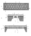
図1は、本発明に係るシリコン基板の加工方法を用いて製造することができるヘッド用基板を備える液体吐出ヘッドの構成を示す概略図である。図1(a)は、上方から見た模式図である。図1(b)は図1(a)のA−A’における概略断面図である。図1(c)は図1(a)のB−B’における概略断面図である。 FIG. 1 is a schematic view showing a configuration of a liquid discharge head including a head substrate that can be manufactured by using the silicon substrate processing method according to the present invention. FIG. 1A is a schematic view seen from above. FIG. 1B is a schematic cross-sectional view taken along line A-A ′ of FIG. FIG.1 (c) is a schematic sectional drawing in B-B 'of Fig.1 (a).
図1において、液体吐出ヘッドは、シリコン基板から構成されるヘッド用基板1と、流路形成部材7と、を少なくとも含んで構成される。
In FIG. 1, the liquid discharge head includes at least a
流路形成部材7は、液体を吐出する吐出口2と、吐出口2と連通する液体流路3と、を構成する。流路形成部材7の上面には吐出性能を向上するために撥液層8が形成されている。
The flow
ヘッド用基板1は、液体流路3に液体を供給するための第2の凹部としての供給口5と、供給口5に連通する第1の凹部としての共通液室4と、を構成する。第2の凹部としての供給口5は、第1の凹部としての共通液室4の底面に複数形成されている。また、第1の凹部としての共通液室4は、流路形成部材7が配置される面(第1の面)と反対側の面(第2の面)に形成されている。第2の凹部としての供給口5は第1の凹部としての共通液室4の底面にヘッド用基板1を貫通して形成されている。
The
ヘッド用基板1と流路形成部材7は、供給口5と液体流路3が連通するように、接着剤18を介して接着されている。また、ヘッド用基板1の上面(第1の面とも称す)にはシリコン酸化膜12が形成されている。
The
ヘッド用基板1は、液体を吐出するための電気熱変換素子等の吐出エネルギー発生素子16を有し、また該吐出エネルギー発生素子を駆動させるための配線等(不図示)を含むことができる。吐出エネルギー発生素子16は吐出口2の位置に対応するようにヘッド用基板1に形成されている。
The
また、共通液室4の底面と側面との角度α(図1(b)及び(c)参照)は90°<α<180°の範囲であり、鈍角である。
Moreover, the angle α (see FIGS. 1B and 1C) between the bottom surface and the side surface of the
共通液室4は、特に制限されるものではないが、例えば結晶異方性エッチングにより形成することができる。結晶異方性エッチングを用いることにより、生産性良く、効率的にヘッド用基板に共通液室(第1の凹部)を形成することができる。共通液室4を結晶異方性エッチングにより形成した場合、αは約54.7°である。また、ヘッド用基板は、<100>面の結晶方位を有するシリコン基板を用いて構成されることができる。この場合、共通液室4の底面はシリコン基板の結晶異方性エッチングより形成された<100>面となる。また、シリコン基板の厚さは、例えば0.3mm〜1.0mmとすることができる。また、共通液室の深さは、例えば0.2mm〜0.9mmとすることができる。
The
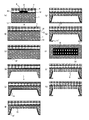
以下、図1に示す液体吐出ヘッドの製造方法について図3を用いて説明する。 Hereinafter, a method for manufacturing the liquid discharge head shown in FIG. 1 will be described with reference to FIGS.
まず、図3(a)及び(b)に示すように、<100>面の結晶方位を有し、まだ共通液室が形成されていないシリコン基板1を用意する。このシリコン基板1は吐出エネルギー発生素子16を有し、第1の面としての上面側に、液体流路の流路型材(又は流路型構造とも称す)6と該流路型材6を覆うように形成された流路形成部材7とを有する。流路形成部材7の上面には撥液層8が形成されており、さらに撥液層8の上面はエッチング耐性のある保護膜9により保護されている。また、ヘッド用基板1の第2の面側には第1の耐エッチング膜13が形成されている。第1の耐エッチング膜13は例えばポリエーテルアミドを用いて形成することができる。
First, as shown in FIGS. 3A and 3B, a
なお、図3(a)は、図1(a)のA−A’線における断面に相当する。また、図3(b)は、図1(a)のB−B’線における断面に相当する。また、図3(b)において、流路型材6は省略されている。
3A corresponds to a cross section taken along the line A-A ′ of FIG. FIG. 3B corresponds to a cross section taken along line B-B ′ of FIG. Moreover, in FIG.3 (b), the flow-path type |
次に、図3(c)に示すように、第1の耐エッチング膜13をパターニングして、共通液室を形成するための第1のエッチングマスク13’を形成する。
Next, as shown in FIG. 3C, the first etching-
次に、図3(d)に示すように、第1のエッチングマスク13’を用いてヘッド用基板1の裏面(第二の面)に結晶異方性エッチングを用いて第1の凹部としての共通液室4を形成する。また、共通液室4を形成する方法としては、特に結晶異方性エッチングに限定されるものではなく、他にも、例えばレーザ加工、ドライエッチングなどを用いることができる。
Next, as shown in FIG. 3D, the first concave portion is formed by using crystal anisotropic etching on the back surface (second surface) of the
次に、図3(e)に示すように、共通液室4の底面に、第2の耐エッチング膜14を形成する。そして、図3(f)に示すように、第2の耐エッチング膜14をパターニングして、共通液室4の底面に供給口を形成するための第2のエッチングマスク14’を形成する。第2のエッチングマスク14’は供給口の形成位置に合わせてパターン開口10を有する。
Next, as shown in FIG. 3E, a second etching
第2のエッチングマスク14’は、例えば、エッチング耐性の優れたレジストを塗布し、露光、現像することにより形成することができる。レジストとしては、例えば、ノボラック樹脂誘導体やナフトキノンジアジド誘導体を用いることができる。ノボラック樹脂誘導体やナフトキノンジアジド誘導体は、シリコンのエッチング液やエッチングガスに対する耐性に優れ、且つ、共通液室である凹み形状の側面に対しても薄膜で均一に被覆可能な材料であるため、好ましく用いることができる。 The second etching mask 14 'can be formed, for example, by applying a resist having excellent etching resistance, exposing and developing. As the resist, for example, a novolak resin derivative or a naphthoquinonediazide derivative can be used. Novolac resin derivatives and naphthoquinonediazide derivatives are preferably used because they are excellent in resistance to silicon etching solution and etching gas, and can be uniformly coated with a thin film on the side surface of the concave shape which is a common liquid chamber. be able to.
第2のエッチングマスク14’の厚さは、特に制限されるものではなく、数μmの厚みでも耐エッチング膜として機能するものであれば特に問題なく使用することができる。 The thickness of the second etching mask 14 'is not particularly limited, and can be used without any problem as long as it functions as an etching resistant film even with a thickness of several micrometers.
また、レジストの塗布方法としては、例えばスピンコート法、ディップコート法、スプレーコート法等を用いて成膜することができる。これらの中でも、傾斜のある凹部側面に対する被覆性を考慮すると、スプレーコート法を用いて成膜することが好ましい。スプレーコート法ではレジスト液を霧状に噴霧することで傾斜面へ均一に被覆することが可能である。さらに、シリコン基板を加熱しながらレジスト液をスプレーすることで、レジスト液が傾斜面に付着後瞬時に溶媒が蒸発し、傾斜面における液ダレや液溜まりを発生させることなくレジストを均一に塗布することが可能である。 In addition, as a resist coating method, for example, a spin coating method, a dip coating method, a spray coating method, or the like can be used. Among these, it is preferable to form a film using a spray coating method in consideration of the coverage with respect to the inclined concave side surface. In the spray coating method, the inclined surface can be uniformly coated by spraying the resist solution in a mist form. Furthermore, by spraying the resist solution while heating the silicon substrate, the solvent evaporates instantly after the resist solution adheres to the inclined surface, and the resist is uniformly applied without causing dripping or pooling of the inclined surface. It is possible.
レジストが塗布された共通液室の底面へのパターンの露光には、例えば、プロキシミティー露光、プロジェクション露光又はステッパ露光等を用いることができる。 For example, proximity exposure, projection exposure, stepper exposure, or the like can be used for pattern exposure on the bottom surface of the common liquid chamber coated with the resist.
パターンを現像する際には、例えばディッピング方式やパドル方式、スプレー方式等を用いて現像液に浸漬させることができる。 When developing a pattern, it can be immersed in a developing solution using a dipping method, a paddle method, a spray method, etc., for example.
次に、図3(g)に示すように、共通液室4が形成されたシリコン基板の裏面(第2の面)にドライフィルムレジストをテンティングラミネートする。
Next, as shown in FIG. 3G, a dry film resist is tented and laminated on the back surface (second surface) of the silicon substrate on which the
次に、図3(h)に示すように、ドライフィルムレジストを露光及び現像することにより、共通液室4の側面を遮蔽しかつ第2のパターニングマスクのパターン開口10を遮蔽しないような遮蔽物11’を形成する。露光には、プロキシミティー露光およびプロジェクション露光を用いることができる。図3(i)は、図3(h)の第2の面側(裏面側)から見た模式図である。図3(h)及び(i)において、遮蔽物11’は、共通液室4へのシリコン基板に垂直な光の照射により形成される陰影が凹部側面を覆いかつパターン開口10は覆わないように第2の面に形成されている。
Next, as shown in FIG. 3H, the dry film resist is exposed and developed to shield the side surface of the
次に、図3(j)に示すように、パターン開口10を有するレジストパターンが形成された共通液室4の底面に対してドライエッチングを行い、複数の供給口5を形成する。
Next, as shown in FIG. 3J, dry etching is performed on the bottom surface of the
ドライエッチングとしては、例えば、ECRやICP等をプラズマ源としたRIEのドライエッチングを用いることができる。また、垂直に例えば100μm以上の供給口を形成するためにはSF6ガスによるエッチングとC4F8ガスによるデポジションを繰り返すボッシュプロセスでICP等のエッチャーを用いることが好ましいが、これに限られるものではない。 As the dry etching, for example, RIE dry etching using ECR or ICP as a plasma source can be used. In order to form a supply port of, for example, 100 μm or more vertically, it is preferable to use an etcher such as ICP in a Bosch process in which etching with SF 6 gas and deposition with C 4 F 8 gas are repeated. It is not a thing.
遮蔽物11’と第2のパターニングマスク14’は必要に応じて取り除くことができる。なお、この際、基板表面の液体流路壁7および撥液層8をエッチング液から保護する目的で、保護層として、エッチング液耐性を有する樹脂等を基板表面に形成しても良い。
The shield 11 'and the second patterning mask 14' can be removed as necessary. At this time, for the purpose of protecting the liquid
次に、図3(k)に示すように、供給口5の底面に露出するシリコン酸化膜12の除去を行う。シリコン酸化膜12のエッチングとしてはフッ酸によるウェットエッチングを行うことができる。
Next, as shown in FIG. 3K, the
その後、流路型構造6を除去し、液体流路3を形成する。この工程では、例えば、流路型構造6に電離放射線を照射し、流路型構造6の分解反応を起こすことで、除去液に対する溶解性を向上させることができる。電離放射線としては、流路型構造6のパターニングの際に使用したものと同様のものを使用できる。ただし、本工程では流路型構造6を除去して液体流路3を形成することが目的であるため、電離照射線はマスクを介さずに全面に照射することができる。その後、流路型構造6のパターニングの際に使用した現像液と同様のものを用いて、流路型構造6を完全に除去することができる。
Thereafter, the
以上の工程により、液体吐出ヘッドを作製することができる。 Through the above steps, a liquid discharge head can be manufactured.
また、本実施形態のシリコン基板の加工方法を液体吐出ヘッドの製造に応用することにより、高い液体のリフィル性能を有する液体吐出ヘッドを製造することができる。また、第2の凹部としての供給口を位置精度高く形成できるため、供給口の位置公差を小さくすることが可能となり、ヘッド用基板の大きさを小さくすることができる。その結果、コストダウンを図ることができる。 In addition, by applying the silicon substrate processing method of this embodiment to the manufacture of a liquid discharge head, a liquid discharge head having high liquid refill performance can be manufactured. In addition, since the supply port as the second recess can be formed with high positional accuracy, the positional tolerance of the supply port can be reduced, and the size of the head substrate can be reduced. As a result, cost reduction can be achieved.
(実施形態2)
また、本発明の実施形態の一つとして、側面にシースが沿うように形成されることを阻害する形状となるように共通液室等の第1の凹部を形成することにより、側面に沿うようなシースが形成されないようにドライエッチングを行うことができる。
(Embodiment 2)
Further, as one embodiment of the present invention, by forming the first concave portion such as the common liquid chamber so as to prevent the sheath from being formed along the side surface, the first side recess is formed along the side surface. Dry etching can be performed so that a proper sheath is not formed.
つまり、本実施形態では、図6(e)に示すような形状を有する共通液室4等の第1の凹部に対してドライエッチングを行う。本実施形態における第1の凹部の形状は、面方向と平行な面によるシリコン基板の第1の凹部部分の断面のうち、開口面積が第1の凹部の開口面より大きくかつ最大となる第1の断面を有する。また、該第1の断面は開口面と底面との間にあり、底面と該底面から前記第1の断面までの第1の側面との角度は鈍角をなす。本実施形態では、前記第1の断面から前記開口面までの第2の側面を構成するシリコン基板部分が遮蔽構造として機能する。
That is, in the present embodiment, dry etching is performed on the first concave portion such as the
本実施形態における方法では、シリコン基板に形成する第1の凹部自体が側壁を遮蔽する形状に加工するため、別途に遮蔽物を形成する必要がない。 In the method according to the present embodiment, since the first recess itself formed in the silicon substrate is processed into a shape that shields the side wall, it is not necessary to separately form a shielding object.
また、本実施形態における第1の凹部は、第1の凹部への第2の面と垂直な光の照射により形成される陰影が前記第1の側面の少なくとも一部を覆いかつレジストパターンのパターン開口には形成されない形状である。 Further, in the first recess in the present embodiment, a shadow formed by irradiation of light perpendicular to the second surface on the first recess covers at least a part of the first side surface, and the pattern of the resist pattern The shape is not formed in the opening.
また、第1の凹部は、前記陰影が前記第1の側面の全てを覆うように形成されていることが好ましいが、特にこれに限定されるものではない。 Moreover, although it is preferable that the 1st recessed part is formed so that the said shadow may cover all the said 1st side surfaces, it is not limited to this in particular.
第1の凹部の底面にドライエッチングを用いて第2の凹部を形成する工程において、前記第1の凹部が図6(e)に示すようなヒサシ形状に形成されていると、実施形態1の遮蔽物と同じ理由により、側面の傾きの影響をほとんど受けず、ヒサシの位置を間口とした垂直な凹部があるのとほぼ同じシースの状態が形成される。これにより、シースの歪みが緩和され、イオンが凹部の側面方向に引き寄せられず、供給口エッチングの際、側壁の堆積膜の一部をエッチングする割合が低くなる。したがって、横方向にずれたエッチングが進まなくなり、垂直にシリコン基板をエッチングすることが可能となる。 In the step of forming the second recess using dry etching on the bottom surface of the first recess, if the first recess is formed in a scissor shape as shown in FIG. For the same reason as that of the shielding object, the sheath state is almost the same as the case where there is a vertical concave portion with the position of the eagles as the frontage, hardly affected by the inclination of the side surface. Thereby, the distortion of the sheath is alleviated, ions are not attracted toward the side surface of the concave portion, and the rate of etching a part of the deposited film on the side wall is reduced during the supply port etching. Therefore, the etching shifted in the lateral direction does not proceed and the silicon substrate can be etched vertically.
また、ヒサシ形状部分で前記第1の側面が遮蔽されない面積が大きくなると、前記第1の側面に形成されるシースにイオンが影響を受けながらエッチングが進行し、供給口等の第2の凹部が傾いて形成されるようになる。ここで、第1の凹部の深さをt、開口面と前記第1の側面との角度をθとすると、遮蔽物を形成しないで供給口を形成した時、共通液室の側面から最も近い、底面端部から0.15tの所に位置する供給口の傾きは2°であった。また、ヒサシ形状部分が第1の側面を全て覆い、供給口を形成した場合、共通液室の側面から最も近い供給口の傾きは0°であった。ヒサシ形状部分が共通液室の側面を遮蔽する範囲と共通液室の側面近傍に位置する供給口の傾きの関係より、底面端部から0.15t以上の距離にある供給口が90°±0.5°の垂直に形成されるには、共通液室の底面端部からt/4tanθの範囲に開口面端部が入っていれば垂直に形成される。つまり、第1の凹部の開口面は矩形状であり、面方向に垂直であって前記開口面の辺に平行な面による断面のいずれにおいても、下記範囲となれば垂直(90°±0.5°)に第2の凹部を第1の凹部の底面に形成することができる。つまり、前記第1の側面に形成される前記陰影の端部が、前記底面の端部から面方向にt/4tanθ(t:前記第1の凹部の深さ、θ:前記開口面と前記第1の側面との角度)までの範囲にあることが好ましい。さらに、供給口のパターンは第1の凹部の中央寄りに形成されることが好ましい。 In addition, when the area where the first side surface is not shielded by the elongate shape portion increases, etching proceeds while the ions are affected by the sheath formed on the first side surface, and the second recess such as the supply port is formed. It will be tilted. Here, when the depth of the first recess is t and the angle between the opening surface and the first side surface is θ, when the supply port is formed without forming a shielding object, the closest to the side surface of the common liquid chamber The inclination of the supply port located 0.15 t from the bottom end was 2 °. In addition, when the elongate shape portion covered the first side surface and formed the supply port, the inclination of the supply port closest to the side surface of the common liquid chamber was 0 °. Due to the relationship between the range in which the shade-shaped portion shields the side surface of the common liquid chamber and the inclination of the supply port located near the side surface of the common liquid chamber, the supply port at a distance of 0.15 t or more from the bottom end is 90 ° ± 0. In order to form a vertical angle of 5 °, if the end of the opening surface is in the range of t / 4 tan θ from the bottom of the common liquid chamber, the vertical is formed. That is, the opening surface of the first recess has a rectangular shape, and is vertical (90 ° ± 0.0) in any of the cross sections of the surface perpendicular to the surface direction and parallel to the sides of the opening surface. 5 °), the second recess can be formed on the bottom surface of the first recess. That is, the end portion of the shadow formed on the first side surface is t / 4 tan θ (t: the depth of the first recess, θ: the opening surface and the first portion in the plane direction from the end portion of the bottom surface. It is preferable that the angle is in the range up to 1). Furthermore, the supply port pattern is preferably formed near the center of the first recess.
本実施形態における第1の凹部は、例えば、シリコン基板の第2の面側に先導孔を形成した後、結晶性異方性エッチングを行うことにより形成することができる。先導孔は、レーザを用いて形成することができる。また、先導孔は、シリコン基板の第2の面をドライエッチングを用いてエッチングすることにより形成することができる。 The first recess in this embodiment can be formed, for example, by forming a leading hole on the second surface side of the silicon substrate and then performing crystalline anisotropic etching. The leading hole can be formed using a laser. The lead hole can be formed by etching the second surface of the silicon substrate using dry etching.
前述の範囲を遮蔽するにはドライエッチングやレーザ加工によりシリコン基板の第2の面側に先導孔をあけ、異方性エッチングの時間を調整して共通液室を形成すればよい。エッチング時間が長くなる程遮蔽されない面積が大きくなってしまうので、前述の範囲内で遮蔽するためには、先導孔の幅と深さ、結晶異方性エッチングの時間を制御してエッチングを行って共通液室を形成する。遮蔽面積を大きくするためにエッチングマスクの内周に近接するように先導孔を形成するのが好ましい。 In order to shield the aforementioned range, a common hole may be formed by making a leading hole on the second surface side of the silicon substrate by dry etching or laser processing and adjusting the anisotropic etching time. The longer the etching time, the larger the area that is not shielded. Therefore, in order to shield within the aforementioned range, the width and depth of the leading hole and the time of crystal anisotropic etching are controlled to perform etching. A common liquid chamber is formed. In order to increase the shielding area, it is preferable to form the leading hole so as to be close to the inner periphery of the etching mask.
以下、本実施形態の製造方法により作製される液体吐出ヘッドの構成について説明する。 Hereinafter, the configuration of the liquid discharge head manufactured by the manufacturing method of the present embodiment will be described.
図5(a)は、本実施形態により製造される液体吐出ヘッドの上面模式図である。図5(b)は、図5(a)の点線A−A’における概略断面図である。図5(c)は、図5(a)の点線B−B’における概略断面図である。 FIG. 5A is a schematic top view of the liquid discharge head manufactured according to this embodiment. FIG. 5B is a schematic cross-sectional view taken along a dotted line A-A ′ in FIG. FIG. 5C is a schematic cross-sectional view taken along a dotted line B-B ′ in FIG.
図5において、液体吐出ヘッドは、シリコン基板から構成されるヘッド用基板1と、流路形成部材7と、を少なくとも含んで構成される。
In FIG. 5, the liquid ejection head includes at least a
流路形成部材7は、液体を吐出する吐出口2と、吐出口2と連通する液体流路3と、を構成する。流路形成部材7の上面には吐出性能を向上するために撥液層8が形成されている。
The flow
ヘッド用基板1は、液体流路3に液体を供給するための第2の凹部としての供給口5と、供給口5に連通する第1の凹部としての共通液室4と、を構成する。第2の凹部としての供給口5は、第1の凹部としての共通液室4の底面に複数形成されている。また、第1の凹部としての共通液室4は、流路形成部材7が配置される面(第1の面)と反対側の面(第2の面)に形成されている。第2の凹部としての供給口5は第1の凹部としての共通液室4の底面にヘッド用基板1を貫通して形成されている。
The
共通液室4の形状は、面方向と平行な面によるシリコン基板の共通液室部分の断面のうち、開口面積が開口面より大きくかつ最大となる第1の断面を有する。また、該第1の断面は開口面と底面との間にあり、底面と該底面から前記第1の断面までの第1の側面との角度は鈍角をなす。共通液室がこのようなヒサシ形状に形成されていると、側面の傾きの影響をほとんど受けず、ヒサシの位置を間口とした垂直な凹部があるのとほぼ同じシースの状態が形成される。
The shape of the
ヘッド用基板1と流路形成部材7は、供給口5と液体流路3が連通するように、接着剤6を介して接着されている。また、ヘッド用基板1の上面(第1の面とも称す)にはシリコン酸化膜12が形成されている。
The
ヘッド用基板1は、液体を吐出するための電気熱変換素子等の吐出エネルギー発生素子16を有し、また該吐出エネルギー発生素子を駆動させるための配線等(不図示)を含むことができる。吐出エネルギー発生素子16は吐出口2の位置に対応するようにヘッド用基板1に形成されている。
The
また、共通液室4の底面と前記第1の側面との角度β(図5(b)及び(c)参照)は90°<α<180℃の範囲であり、鈍角である。
(実施形態3)
実施形態1において、遮蔽物を供給口を形成する部分を含んだ最小限の領域のみを開口し、その他の領域には全て残すという例を記載した。これをシリコン基板の一部を用いて同様の効果を得るのが、本実施形態である。
Further, the angle β (see FIGS. 5B and 5C) between the bottom surface of the
(Embodiment 3)
In the first embodiment, an example has been described in which only a minimum region including a portion that forms the supply port is opened in the shield and all other regions are left. In this embodiment, the same effect is obtained by using a part of the silicon substrate.
即ち、ヘッド用基板に、共通液室を形成したもう一枚のシリコン基板を開口部が内側になるように接合し、シリコン基板自身をシースの歪みを抑制する遮蔽物として使用するという考え方である。 That is, it is an idea that another silicon substrate having a common liquid chamber is bonded to the head substrate so that the opening is on the inside, and the silicon substrate itself is used as a shield for suppressing the distortion of the sheath. .
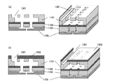
まず、図11(a)に示すように、第1の面と該第1の面と反対側の第2の面を有する第1のシリコン基板1101に、予め第1の凹部1102(共通液室)を、第一のシリコン基板1101が貫通しないように第2の面側に形成する。第1の凹部は熱酸化処理によってシリコン酸化膜を設けてもよい。シリコン酸化膜を設けることによりインク耐久性を向上することができる。
First, as shown in FIG. 11A, a first recess 1102 (common liquid chamber) is previously formed in a
次に、図11(b)に示すように、第2のシリコン基板1103に中間層1104を形成し、供給口のパターン開口(第1のパターン開口)1105を中間層1104に形成する。
Next, as illustrated in FIG. 11B, the
次に、図11(c)に示すように、第2のシリコン基板1103と、第1のシリコン基板1101の第1の凹部1102が開口している側の面(第2の面)を、中間層1104を介して接合する。
Next, as shown in FIG. 11C, the
次に、第1のシリコン基板の中間層1104と反対側の面(第1の面)上に、第2のパターニングマスクを形成する。該第2のパターニングマスクの第2のパターン開口は、第1のパターン開口の面方向と垂直な位置を含む開口パターンで形成されている。
Next, a second patterning mask is formed on the surface (first surface) opposite to the
次に、図11(d)に示すように、第1のシリコン基板1101側から、第2のパターニングマスクを用いて貫通孔1106をシリコンエッチングにより形成する。前記中間層の第1のパターン開口に対応する領域に貫通孔1106が形成される。
Next, as shown in FIG. 11D, a through
次に、図11(e)に示すように、第1のパターン形状1105が形成された中間層1104をマスクとして、第2のシリコン基板1103に供給口1107を反応性イオンエッチングにより形成する。この際、第1のシリコン基板の第1の面が遮蔽構造として機能し、プラズマモールディング効果の影響を低減することができる。
Next, as shown in FIG. 11E, a
以上の工程により、共通液室1102はシリコン基板によってふたをされ、供給口エッチングの最中、プラズマ中にほとんど露出しない状態となる。これにより、シース1108の歪みは大幅に抑制され、垂直な供給口エッチングを実施することが出来る。
Through the above steps, the
中間層の材料としては、特に制限されるものではないが、例えば、樹脂材料、シリコン酸化物(SiO)、シリコン窒化物(SiN)、シリコン酸窒化物(SiON)、シリコン炭化物(SiC)等が挙げられる。つまり、中間層としては、例えば、樹脂層、シリコン酸化膜、シリコン窒化膜、シリコン酸窒化膜、炭化シリコン膜等が挙げられる。樹脂層としては例えば感光性樹脂層が挙げられる。これらの中でも、中間層として、形成が容易であることから、感光性樹脂層やシリコン酸化膜を用いることが好ましい。 The material of the intermediate layer is not particularly limited, and examples thereof include resin materials, silicon oxide (SiO), silicon nitride (SiN), silicon oxynitride (SiON), silicon carbide (SiC), and the like. Can be mentioned. That is, examples of the intermediate layer include a resin layer, a silicon oxide film, a silicon nitride film, a silicon oxynitride film, and a silicon carbide film. Examples of the resin layer include a photosensitive resin layer. Among these, a photosensitive resin layer or a silicon oxide film is preferably used as the intermediate layer because it can be easily formed.
接合の方法に関しては、樹脂材料等による接着、活性化させた表面同士を接触させて自発的に接合が進むフュージョン接合、共晶接合、拡散接合等がある。 Regarding the bonding method, there are adhesion by a resin material, fusion bonding, eutectic bonding, diffusion bonding, etc. in which bonding is activated by bringing activated surfaces into contact with each other.
第2のシリコン基板として、液体吐出エネルギー発生素子を有する基板そのものを用いることが出来る。基板の厚みは、例えば50〜800μmである。供給口の形状の観点から、100〜200μmとすることが好ましい。所望の厚みにするために、接合前に基板を薄板化することも出来る。薄板化する方法としては、バックグラインド等の機械的研磨、CMP、ウェットエッチング又はドライエッチング、あるいはそれらの組み合わせ等が挙げられる。必要に応じて、目の細かい機械的研磨、化学的研磨、あるいはそれらの組み合わせ等によって、表面を鏡面状に仕上げることができる。流路型構造6、液体流路壁7を用いて形成された吐出口2と撥液層8を有する流路形成層1109は、供給口エッチングの前、即ち図11(c)と(d)の間に形成することが望ましい。流路形成層を含んだプロセス完了後の斜視図を図11(f)に示す。
As the second silicon substrate, a substrate itself having a liquid discharge energy generating element can be used. The thickness of the substrate is, for example, 50 to 800 μm. From the viewpoint of the shape of the supply port, the thickness is preferably 100 to 200 μm. In order to obtain a desired thickness, the substrate can be thinned before bonding. Examples of the thin plate method include mechanical grinding such as back grinding, CMP, wet etching or dry etching, or a combination thereof. If necessary, the surface can be mirror-finished by fine mechanical polishing, chemical polishing, or a combination thereof. The flow
また、図12に示すように、第2のシリコン基板として液体吐出エネルギー発生素子を有する基板以外のものを用いて、更に薄板化した液体吐出エネルギー発生素子を有する基板を接合するという方法もある。薄板化した後の基板に中間層の形成を行うのは、プロセス装置の搬送系の制限により難しい場合もある。それに対して、例えば第1のシリコン基板1101と第2のシリコン基板1103を接合(図12(a))した後、第2のシリコン基板を薄板化し(図12(b))、その後に同じく薄板化された液体吐出エネルギー発生素子を有する基板1201と接合する(図12(c))という方法が考えられる。この第2のシリコン基板1103と、液体吐出エネルギー発生素子を有する基板との板厚合計が、50〜800μmで、望ましくは100〜200μmとなるように形成する。第2のシリコン基板とヘッド基板との接合は、直接接合も可能であるが、中間層を用いても構わない。流路形成層は、同じく、供給口エッチングの前に形成することが望ましい。
In addition, as shown in FIG. 12, there is a method of using a substrate other than the substrate having the liquid discharge energy generating element as the second silicon substrate and bonding the substrate having the liquid discharge energy generating element further thinned. It may be difficult to form the intermediate layer on the thinned substrate due to the limitation of the transport system of the process apparatus. On the other hand, for example, after the
第1のシリコン基板は、第1の凹部1102(共通液室)を形成後に内部にシリコン酸化膜を形成しておくことも出来る。これにより、供給口エッチング時に共通液室内部が多少なりともエッチングされてしまう懸念を排除することが出来る。また酸化膜でシリコンの表面をコーティングすることにより、インク耐性が向上するという利点もある。シリコン酸化膜の形成は、熱酸化、CVD等が挙げられる。 In the first silicon substrate, a silicon oxide film can be formed inside after forming the first recess 1102 (common liquid chamber). As a result, it is possible to eliminate the concern that the common liquid chamber is slightly etched during the supply port etching. In addition, there is an advantage that ink resistance is improved by coating the surface of silicon with an oxide film. Examples of the formation of the silicon oxide film include thermal oxidation and CVD.
以下に、接合方法や中間層について更に詳しく説明する。 Hereinafter, the bonding method and the intermediate layer will be described in more detail.
中間層として樹脂材料を選択した場合、例えば以下の方法によりシリコン基板を接着することができる。まず、シリコン基板に樹脂を塗布、パターニングして中間層を形成した後、該中間層を挟んでシリコン基板を積層させる。そして、ガラス転移温度以上に昇温した状態で圧力を印加し、接着することができる。一般的な樹脂材料は、ほぼ全てがその対象である。樹脂材料としては、例えば、アクリル系樹脂、ポリイミド系樹脂、シリコン系樹脂、フッ素系樹脂、エポキシ系樹脂、ポリエーテルアミド系樹脂等が挙げられる。
アクリル系樹脂としては、例えばPMMA(ポリメチルメタクリレート)樹脂が挙げられる。シリコン系樹脂としては、例えばPDMS(ポリジメチルシロキサン)樹脂が挙げら得る。エポキシ系樹脂としては、例えば、化薬マイクロケム製のSU−8(商品名)が具体的に挙げられる。ポリエーテルアミド系樹脂としては、例えば、日立化成製のHIMAL(商品名)、BCB(Benzocyclobutene)、HSQ(HydrogensSlises−Quioxane)等が具体的に挙げられる。
When a resin material is selected as the intermediate layer, for example, the silicon substrate can be bonded by the following method. First, a resin is applied to a silicon substrate and patterned to form an intermediate layer, and then the silicon substrate is stacked with the intermediate layer interposed therebetween. And it can bond by applying a pressure in the state heated up more than the glass transition temperature. Almost all common resin materials are targeted. Examples of the resin material include acrylic resins, polyimide resins, silicon resins, fluorine resins, epoxy resins, polyether amide resins, and the like.
Examples of the acrylic resin include PMMA (polymethyl methacrylate) resin. An example of the silicon-based resin is PDMS (polydimethylsiloxane) resin. Specific examples of the epoxy resin include SU-8 (trade name) manufactured by Kayaku Microchem. Specific examples of the polyetheramide resin include HIMAL (trade name), BCB (Benzocyclobutene), HSQ (HydrogensSlices-Quixane) manufactured by Hitachi Chemical.
第1のパターン形状を形成する方法については、感光性を有する樹脂材料の場合はリソグラフィー法を用いてパターニングすることができる。感光性を有しない樹脂材料の場合は、エッチングによって行うことができる。シリコンを含まない樹脂層であれば、例えばO2、O2/CF4、O2/Ar、N2、H2、N2/H2,NH3等のガスを用いたプラズマ法にてエッチングできる。シリコンを含有する樹脂層に関しては、それらのガスにCF4、CHF3等のフルオロカーボン系のガスを添加することでエッチングできる。 Regarding the method of forming the first pattern shape, in the case of a resin material having photosensitivity, patterning can be performed using a lithography method. In the case of a resin material having no photosensitivity, it can be performed by etching. If the resin layer does not contain silicon, for example, etching is performed by a plasma method using a gas such as O 2 , O 2 / CF 4 , O 2 / Ar, N 2 , H 2 , N 2 / H 2 , and NH 3. it can. The resin layer containing silicon can be etched by adding a fluorocarbon-based gas such as CF 4 or CHF 3 to these gases.
また、他の接合方法として、接合する表面をプラズマ処理することによってダングリングボンドを形成して接合する、フュージョン接合と呼ばれる方法がある。このフュージョン接合には、大きく分けて2つの方法がある。 As another bonding method, there is a method called fusion bonding in which dangling bonds are formed by performing plasma treatment on the surfaces to be bonded. There are roughly two methods for this fusion bonding.
第一の方法は、中間層の表面をプラズマ処理した後、大気中に曝してOH基を形成し、シリコン基板表面と水素結合を介して接合するものである。OH基は、大気中の水分と反応することにより形成されるが、積極的に水分を付加しても良い。この方法を適用できる中間層の材料としては、例えばシリコン酸化膜やシリコン窒化膜、炭化シリコン等が挙げられる。また、その他、表面に酸化膜を形成し易い金属材料や金属酸化物、一部の樹脂材料などが挙げられる。常温で仮接合を行った後、200〜300℃程度のアニール処理をすることにより、OH基同士の脱水反応によりH2Oが脱離して、O原子を仲介とした強固な接合を得ることができる。ただし、分子間力が及ぶ範囲にまで表面同士を接近させなければならないため、表面粗さにして1nm以下の値を有することが望ましい。 In the first method, the surface of the intermediate layer is subjected to plasma treatment, and then exposed to the atmosphere to form OH groups, which are bonded to the silicon substrate surface via hydrogen bonds. The OH group is formed by reacting with moisture in the atmosphere, but moisture may be positively added. Examples of the material for the intermediate layer to which this method can be applied include a silicon oxide film, a silicon nitride film, and silicon carbide. Other examples include metal materials and metal oxides that easily form an oxide film on the surface, and some resin materials. After performing temporary bonding at room temperature, annealing is performed at about 200 to 300 ° C., whereby H 2 O is desorbed by a dehydration reaction between OH groups to obtain a strong bond mediated by O atoms. it can. However, since the surfaces must be brought close to the range where the intermolecular force reaches, it is desirable that the surface roughness has a value of 1 nm or less.
第2の方法は、水素結合を介さず、真空中でそのままダングリングボンド同士を接合させるものである。この方法も、表面粗さにして1nm以下の値が必要と言われているが、研磨等によりそれを実現できれば、理論上あらゆる材料で接合が可能である。シリコン系の材料では、少なくとも、シリコン酸化膜同士、シリコン窒化膜同士、あるいは、それぞれの膜とシリコンとの接合が確認されている。シリコン酸化膜、シリコン窒化膜のパターニングは、CF4、CHF3、C2F6、C3F8、C4F8、C5F8、C4F6等のフルオロカーボン系のガスを用いたプラズマによって実施することができる。また、シリコン酸化膜は、例えば、フッ酸をベースとしたウェットエッチングによってもパターニングできる。また、シリコン窒化膜は、例えば、熱リン酸を用いたウェットエッチングによってもパターニングできる。また、中間層の材料が金属材料や金属酸化物の場合も、接合前にパターニングを施せるものであれば、本発明に適用できる。 The second method is to join dangling bonds as they are in a vacuum without using hydrogen bonds. This method is also said to have a surface roughness value of 1 nm or less, but theoretically, any material can be used if it can be realized by polishing or the like. In silicon-based materials, at least silicon oxide films, silicon nitride films, or each film and silicon are confirmed to be bonded. For patterning the silicon oxide film and the silicon nitride film, fluorocarbon gases such as CF 4 , CHF 3 , C 2 F 6 , C 3 F 8 , C 4 F 8 , C 5 F 8 , and C 4 F 6 were used. It can be performed by plasma. The silicon oxide film can also be patterned by wet etching based on hydrofluoric acid, for example. Further, the silicon nitride film can be patterned by, for example, wet etching using hot phosphoric acid. Further, even when the material of the intermediate layer is a metal material or a metal oxide, it can be applied to the present invention as long as it can be patterned before bonding.
また、他の接合方法として、共晶接合や拡散接合を用いることもできる。共晶接合であれば、例えば、金と金、金とシリコン、金と錫、金とゲルマニウム、銅と錫、パラジウムとインジウム等の組み合わせが知られている。拡散接合であれば、例えば、金と金、銅と銅、アルミニウムとアルミニウム等の組み合わせが知られている。 Further, as another bonding method, eutectic bonding or diffusion bonding can be used. For eutectic bonding, for example, gold and gold, gold and silicon, gold and tin, gold and germanium, copper and tin, palladium and indium, and the like are known. For diffusion bonding, for example, combinations of gold and gold, copper and copper, aluminum and aluminum, and the like are known.
次に、中間層とシリコン基板とドライエッチングの関係について説明する。 Next, the relationship between the intermediate layer, the silicon substrate, and dry etching will be described.
例えば、ボッシュプロセスを用いた場合、通常のレジストマスクにて50以上のエッチングレート比を容易に得ることができる。例えば中間層に樹脂材料を用いる場合は、材料の組成がレジストマスクに近いため、ほとんどの樹脂材料で同程度の結果が得られる。中間層としての樹脂材料の成膜厚は、例えば数百nm〜数十μm程度であるが、これはシリコンを例えば深さ50〜800μmエッチングするためのマスクやストッパーとしては十分な数値である。 For example, when the Bosch process is used, an etching rate ratio of 50 or more can be easily obtained with a normal resist mask. For example, when a resin material is used for the intermediate layer, since the composition of the material is close to that of a resist mask, almost the same result can be obtained with most resin materials. The film thickness of the resin material as the intermediate layer is, for example, about several hundred nm to several tens of μm, which is a sufficient value as a mask or a stopper for etching silicon to a depth of, for example, 50 to 800 μm.
シリコン酸化膜では、シリコンに対して少なくとも100以上のエッチングレート比が得られることが知られている。シリコン酸化膜は、熱酸化法を用いた場合、例えば25μm以上の膜厚まで形成できることが知られており、膜質やプロセス難易度を考慮すると好ましくは2μm以下の膜厚が望ましい。また、プラズマCVD法を用いた場合、例えば50μm以上の膜厚まで形成できることが知られており、膜質やプロセス難易度を考慮すると好ましくは10μm以下の膜厚が望ましい。これらの膜厚はシリコン酸化膜をマスクとして用いてシリコンを例えば深さ50〜800μmエッチングするには十分な数値である。 It is known that a silicon oxide film can obtain an etching rate ratio of at least 100 or more with respect to silicon. It is known that the silicon oxide film can be formed to a film thickness of, for example, 25 μm or more when the thermal oxidation method is used, and the film thickness of 2 μm or less is desirable in consideration of film quality and process difficulty. In addition, when the plasma CVD method is used, it is known that a film thickness of, for example, 50 μm or more can be formed, and the film thickness of 10 μm or less is desirable in consideration of the film quality and the process difficulty. These film thicknesses are sufficient values for etching silicon to a depth of 50 to 800 μm, for example, using a silicon oxide film as a mask.
シリコン以外の金属や金属酸化物には、シリコンに対してさらに高い選択比が得られるものもある。Fラジカルとの反応性が低い材料が特に好適であり、例えばクロム、アルミ等では1000を超えるエッチングレート比を得られる場合もある。金属又は金属酸化物等の成膜厚は、一般的に数μm程度である。所望のエッチング深さを得るためには、その材料のシリコンとのエッチングレート比を考慮して、成膜厚を適宜選択することが望ましい。 Some metals and metal oxides other than silicon can provide a higher selectivity than silicon. A material having low reactivity with F radicals is particularly suitable. For example, an etching rate ratio exceeding 1000 may be obtained with chromium, aluminum, or the like. The film thickness of a metal or metal oxide is generally about several μm. In order to obtain a desired etching depth, it is desirable to appropriately select the film thickness in consideration of the etching rate ratio of the material to silicon.
また、本実施形態の方式を用いると、基板裏面からの液体の導入口を、供給口と二次元的に重ならない位置に配置することが出来る。液体吐出エネルギー発生素子を有する基板と液体供給タンク(図示無し)を接続する中間体として、例えばアルミナの板を加工したものを用いている。アルミナ板の加工精度は、フォトリソを用いた半導体プロセスには遠く及ばないため、共通液室のサイズやチップサイズの縮小によって、その位置に対応したアルミナの加工が困難になる場合がある。 Further, when the system of the present embodiment is used, the liquid inlet from the back surface of the substrate can be arranged at a position where it does not overlap two-dimensionally with the supply port. As an intermediate that connects a substrate having a liquid discharge energy generating element and a liquid supply tank (not shown), for example, an alumina plate processed is used. Since the processing accuracy of the alumina plate is far from that of a semiconductor process using photolithography, it may be difficult to process the alumina corresponding to the position by reducing the size of the common liquid chamber or the chip size.
本実施例では、共通液室が予め基板内部に形成されている。そのため、後から共通液室に接続可能な任意の位置に開口1301を設けることが出来る(図13(a))。これにより、共通液室と液体供給タンクとの接続口を、任意の位置に再配置することが可能となる。なお、供給口のエッチングのため第1のシリコン基板に形成した開口1301は、例えばアルミナ板1302によってふたをすることにより、封止することが出来る(図13(b))。
In this embodiment, the common liquid chamber is formed in advance in the substrate. Therefore, the
本実施形態において、図11(d)には、第2のシリコン基板と、該第2のシリコン基板の上に設けられた前記パターニングマスクとしての中間層と、該中間層の上に設けられ、前記パターン開口が露出する第1の開口と該第1の開口及び前記中間層と反対側の面に連通する貫通孔とを有する第1のシリコン基板と、を含む積層構造が示されている。貫通孔は、前記パターン開口の面方向と垂直な位置を含む開口パターンで形成されている。そして本実施形態では、貫通孔側から反応性イオンエッチングを行い、前記第2のシリコン基板に前記第2の開口を形成している。第1のシリコン基板の第1の面が遮蔽構造として機能することがわかる。
(実施形態4)
実施形態3と同様にシリコン基板の一部を用いてプラズマモールディング効果の抑制効果を得る、別の例を本実施形態に示す。
In the present embodiment, FIG. 11D shows a second silicon substrate, an intermediate layer as the patterning mask provided on the second silicon substrate, and provided on the intermediate layer. A laminated structure including a first opening in which the pattern opening is exposed and a first silicon substrate having a through hole communicating with the surface opposite to the first opening and the intermediate layer is shown. The through hole is formed in an opening pattern including a position perpendicular to the surface direction of the pattern opening. In the present embodiment, reactive ion etching is performed from the through-hole side to form the second opening in the second silicon substrate. It can be seen that the first surface of the first silicon substrate functions as a shielding structure.
(Embodiment 4)
As in the third embodiment, another example in which the suppression effect of the plasma molding effect is obtained using a part of the silicon substrate is shown in this embodiment.
即ち、ヘッド用基板に、共通液室を形成するためのもう一枚のシリコン基板を接合し、共通液室を形成するパターンの中にダミーパターンを入れて実質的な開口幅を減少させ、シースの歪みを抑制するという考え方である。 That is, another silicon substrate for forming the common liquid chamber is bonded to the head substrate, and a dummy pattern is inserted into the pattern forming the common liquid chamber to reduce the substantial opening width, and the sheath This is the idea of suppressing the distortion.
まず、図15(a)に示すように、第1のシリコン基板1501の表面にある中間層1503に、供給口のパターンを有する第1のパターン開口1504を形成する。
First, as shown in FIG. 15A, a
次に、図15(b)に示すように、第2のシリコン基板1502と第1のシリコン基板1501を、中間層1503を介して接合する。
Next, as shown in FIG. 15B, the
その後、図15(c)に示すように、第1のシリコン基板1501側に、共通液室を形成するための第2のパターン開口1505を有する第2のパターニングマスクを形成する。この第2のパターニングマスクのパターンの中には、プラズマモールディング効果を抑制するためのダミー構造を形成するための第3のパターン1506が含まれる。
Thereafter, as shown in FIG. 15C, a second patterning mask having a second pattern opening 1505 for forming a common liquid chamber is formed on the
次に、図15(d)に示すように、第2のパターニングマスク用いて共通液室1507をシリコンエッチングにより形成する。シリコンエッチングとしては、反応性イオンエッチングを用いることが好ましい。
Next, as shown in FIG. 15D, the
次に、第1のパターン開口1504を有する中間層1503をマスクとして、反応性イオンエッチングにより供給口1508を形成する。
Next, the
ダミーパターン1506により形成されるダミー構造の配置としては、インクの供給を妨げない範囲であれば任意の形状を取ることができ、例えば図15(e)に示すようにドット状のアレイ構造等が適している。
The arrangement of the dummy structure formed by the
つまり、前記第1のシリコン基板の第1の面上に形成された前記第2のパターニングマスクは、共通液室の外壁(側壁)を形成するための側壁パターンと、前記ダミー構造を形成するためのダミーパターンを含む。そして、該ダミーパターンは前記側壁パターン内であって、かつ前記中間層に設けられているパターン開口の面方向と垂直な位置以外の領域に配置されている。 That is, the second patterning mask formed on the first surface of the first silicon substrate forms a sidewall pattern for forming the outer wall (sidewall) of the common liquid chamber and the dummy structure. Including dummy patterns. The dummy pattern is arranged in a region other than the position in the side wall pattern and perpendicular to the surface direction of the pattern opening provided in the intermediate layer.
ダミー構造は、共通液室内であって中間層1503の第1のパターン開口1504以外の領域に設けられる。例えば、ダミー構造は、共通液室内に柱状に複数設けることができる。該共通液室内に形成されたダミー構造が遮蔽構造として機能し、プラズマモールディング効果の影響を低減することができる。
The dummy structure is provided in a region other than the first pattern opening 1504 of the
接合工程、中間層の材料、エッチングの方法等に関しては、実施形態3に準ずる。 The bonding process, intermediate layer material, etching method, and the like are the same as in the third embodiment.
以上の工程により、共通液室1507のエッチングは、実質的に本来の開口幅よりも狭い開口幅でエッチングすることになり、シース1509の歪みは大幅に抑制され、垂直な供給口エッチングを実施することが出来る。
Through the above steps, the etching of the
(実施例1)
実施形態1における実施例として、図3で示す液体吐出ヘッドの製造方法によって液体吐出ヘッドを製造した。
Example 1
As an example in
表面に(100)面を持ち、液体吐出エネルギー発生素子16、流路型構造6、液体流路壁7を用いて形成された吐出口2と撥液層8が形成されているヘッド用基板1を用意する。
A
まず、撥液層8上に、保護層9としてOBC(商品名、東京応化製)を全面に塗布した(図3(a、b))。次いで、ヘッド用基板1の裏面にポリエーテルアミド樹脂(日立化成製HIMAL(商品名))からなる耐エッチング膜13を形成した。
First, OBC (trade name, manufactured by Tokyo Ohka Kogyo Co., Ltd.) was applied as a
次いで、耐エッチング膜13上に感光性ポジ型レジスト(東京応化製OFPR−800(商品名))を全面に塗布した。塗布したポジ型レジストに対してウシオ電機製Deep−UV露光装置UX−3000(商品名)を用いてスリットの状供給口パターンを形成した。次に、CF4とO2の混合ガスを用い、ポジ型レジスト上からケミカルドライエッチングにより耐エッチング膜13をスリット状の供給口パターンに形成し、第1のエッチングマスク13’を形成した(図3(c))。
Next, a photosensitive positive resist (OFPR-800 (trade name) manufactured by Tokyo Ohka Kogyo Co., Ltd.) was applied on the entire surface of the etching
次に、供給口パターンが形成された第1のエッチングマスク13’をマスクとして、80℃のテトラメチルアンモニウムハイドロオキサイド水溶液中に浸漬することでシリコン基板に対して異方性エッチングを行い、共通液室4を形成した(図3(d))。なお、異方性エッチングは、形成される共通液室4の深さが475μmになるように、エッチングレートを計算し浸漬を行った。なお、エッチングマスクは基板を用意する際に、あらかじめ形成されていてもよい。
Next, the silicon substrate is anisotropically etched by being immersed in a tetramethylammonium hydroxide aqueous solution at 80 ° C. using the
次いで、第1のエッチングマスク13’を除去した。 Next, the first etching mask 13 'was removed.
次に、異方性エッチングを行った表面に対して、スプレーコータ(イーヴィーグループ社製)を用いて感光性のポジ型レジスト層14を形成した(図3(e))。感光性ポジ型レジストとしてはAZ−P4620(AZエレクトロニックマテリアルズ社製、商品名)を用いた。スプレーコート時に基板が60℃に保つように基板チャックを加熱しながら塗布を行うことで、傾斜およびエッジ部に均一に塗布した。
Next, a photosensitive positive resist
次いで、感光性ポジ型レジスト14に対してウシオ電機製投影露光装置UX−4023(商品名)を用いて1000mJ/cm2の露光量で供給口パターンのマスクを通して露光を行った。この際、露光する箇所は、先に異方性エッチングで形成した供給口の底部であるため、露光フォーカス位置を異方性エッチングした深さ分だけ下に設定した。次いで、2.38%のテトラメチルアンモニウムハイドロオキサイド水溶液を用いて現像を行い、共通液室の底面に微細な供給口のパターン開口10が形成された第2のエッチングマスク14’を形成した(図3(f))。
Next, the photosensitive positive resist 14 was exposed through a supply port pattern mask at an exposure amount of 1000 mJ / cm 2 using a projection exposure apparatus UX-4023 (trade name) manufactured by USHIO. At this time, since the portion to be exposed is the bottom of the supply port formed by anisotropic etching previously, the exposure focus position was set downward by the depth of anisotropic etching. Next, development was performed using a 2.38% tetramethylammonium hydroxide aqueous solution to form a
次いで、基板裏面にネガ型感光性ドライフィルムレジスト11(東京応化工業社製、AR−340(商品名))をラミネートした(図3(g))。そして、ウシオ電機製投影露光装置UX−4023(商品名)を用いて、得られる遮蔽物11’が共通液室の開口面端部から336μm張り出したヒサシ形状となるようにパターニングを行った。この開口面端部から336μmのヒサシ状の遮蔽物は、共通液室4の深さが475μmの時、共通液室の開口面端部から共通液室4の底面と側面の境界線までを遮蔽することができる。
Next, a negative photosensitive dry film resist 11 (manufactured by Tokyo Ohka Kogyo Co., Ltd., AR-340 (trade name)) was laminated on the back surface of the substrate (FIG. 3G). Then, using a projection exposure apparatus UX-4023 (trade name) manufactured by USHIO ELECTRIC CO., LTD., Patterning was performed so that the obtained shielding
次いで、1%炭酸ナトリウム水溶液を用いて現像を行い、共通液室の斜面をヒサシ状に遮蔽する遮蔽物11を形成した(図3(h))。遮蔽物11’を形成した後の平面模式図が図3(i)である。
Next, development was performed using a 1% aqueous sodium carbonate solution to form a
次いで、第2のエッチングマスク14’上よりAMS200(ALCATEL社製、商品名)を用いてボッシュプロセスにて基板1を上面のエッチングストップ層であるシリコン酸化膜12までエッチングを行うことで供給口5を形成した(図3(j))。共通液室の斜面に最も近い供給口から6つ目の供給口までの角度は89.7°〜90.3°の範囲であり、平均値は90.0°であった。次いで、エッチングストップ層であるシリコン酸化膜12は、バッファードフッ酸110U(ダイキン工業社製、商品名)により、ウェットエッチングし、除去した(図3(k))。
Next, the
次いで、第2のエッチングマスク14’及び遮蔽物11’は、酸素プラズマによるアッシングで除去し、保護層9であるOBC(商品名)をキシレンにて除去した。その後、ウシオ電機製Deep−UV露光装置UX−3000(商品名)を用いて撥液層8上から7000mJ/cm2の露光量で全面に露光し、液体流路パターンを形成する流路型構造6を可溶化した。そして、乳酸メチル中に超音波を付与しつつ浸漬することで、流路型構造6を除去し、図3(a),(b)に示すような液体吐出ヘッドを作製した。
Next, the
(実施例2)
実施例1では共通液室の傾斜側面のみを遮蔽したが、本実施例では共通液室の傾斜側面に加え、底面まで遮蔽するヒサシ状の遮蔽物を形成した。ヒサシ状の遮蔽物は実施例1と同様の方法で形成し、共通液室の底面にあるレジストパターンのパターン開口は遮蔽しないように共通液室の開口面端部から600μm張り出した形状とした。次いで、実施例1と同様にボッシュプロセスにてエッチングを行うことで供給口5を形成した。
(Example 2)
In Example 1, only the inclined side surfaces of the common liquid chamber were shielded. In this example, in addition to the inclined side surfaces of the common liquid chamber, a shield-like shield that shields the bottom surface was formed. The shield-like shield was formed in the same manner as in Example 1, and had a shape protruding 600 μm from the end of the opening surface of the common liquid chamber so as not to shield the pattern opening of the resist pattern on the bottom surface of the common liquid chamber. Subsequently, the
傾斜側面から3つ目の供給口の角度は89.5°〜89.6°の範囲であり、平均値は89.5°であった。この結果より、遮蔽膜はレジストパターンのパターン開口を遮蔽しなければ、共通液室の底面を遮蔽するまで遮蔽範囲を広げても90°±0.5°の範囲に供給口を形成することができる。 The angle of the third supply port from the inclined side surface was in the range of 89.5 ° to 89.6 °, and the average value was 89.5 °. From this result, if the shielding film does not shield the pattern opening of the resist pattern, the supply port can be formed in a range of 90 ° ± 0.5 ° even if the shielding range is expanded until the bottom surface of the common liquid chamber is shielded. it can.
(実施例3)
本実施例においては、図3で示す製造方法によって、液体吐出ヘッドを製造した。基板1を準備してから、パターン開口10を有する第2のエッチングマスク14’を形成する工程まで、実施例1と同じ工程で形成した(図3(f))。
(Example 3)
In this example, a liquid discharge head was manufactured by the manufacturing method shown in FIG. From the preparation of the
遮蔽物は以下のように形成した。 The shield was formed as follows.
まず、ネガ型感光性ドライフィルムレジスト11(東京応化工業社製、AR−340)をフィルム上に配置し、フィルム状のレジストに対してウシオ電機製露光装置UX−4023(商品名)を用いて、開口が形成されたマスクを通して露光を行った。次いで、1%の炭酸ナトリウム水溶液を用いて現像を行い、開口が形成された感光性ネガ型レジストフィルムを作製した。この開口が形成された感光性ネガ型レジストフィルムを第2のエッチングマスク14’が形成されたヘッド用基板1の第2の面上に、アライメントを行ってロール式ラミネーターで接着させることにより、遮蔽物11’を形成した。
First, a negative type photosensitive dry film resist 11 (AR-340, manufactured by Tokyo Ohka Kogyo Co., Ltd.) is placed on the film, and an exposure apparatus UX-4023 (trade name) manufactured by USHIO INC. Is used for the film-like resist. Then, exposure was performed through a mask in which an opening was formed. Next, development was performed using a 1% aqueous sodium carbonate solution to prepare a photosensitive negative resist film having openings. The photosensitive negative resist film in which the opening is formed is aligned on the second surface of the
次いで、第2のエッチングマスク14’上よりAMS200(ALCATEL社製、商品名)を用いてボッシュプロセスにて基板1をエッチングストップ層であるシリコン酸化膜12までエッチングを行うことで供給口5を形成した。
Next, the
次いで、保護層9であるOBC(商品名)をキシレンにて除去した。その後、ウシオ電機製Deep−UV露光装置UX−3000(商品名)を用いて撥インク層上から7000mJ/cm2の露光量で全面に露光し、流路型構造6を可溶化した。そして、乳酸メチル中に超音波を付与しつつ浸漬することで、流路型構造6を除去し、液体吐出ヘッドを作製した。
Next, OBC (trade name) as the
(実施例4)
実施形態2における実施例として、図7で示す液体吐出ヘッドの製造方法によって液体吐出ヘッドを製造した。
Example 4
As an example in Embodiment 2, a liquid discharge head was manufactured by the method of manufacturing a liquid discharge head shown in FIG.
表面に(100)面を持ち、液体吐出エネルギー発生素子16、流路型構造6、液体流路壁7を用いて形成された吐出口2と撥液層8が形成されているヘッド用基板1を用意する。
A
まず、撥液層8上に、保護層9としてOBC(商品名、東京応化製)を全面に塗布した(図6(a、b))。次いで、基板の裏面にポリエーテルアミド樹脂(日立化成製HIMAL(商品名))からなる耐エッチング膜13を形成した。
First, OBC (trade name, manufactured by Tokyo Ohka Kogyo Co., Ltd.) was applied as a
次いで、耐エッチング膜13上に感光性ポジ型レジスト(東京応化製OFPR−800(商品名))を全面に塗布した。塗布したポジ型レジストに対してウシオ電機製Deep−UV露光装置UX−3000(商品名)を用いてスリット状の供給口パターンを形成した。次に、CF4とO2の混合ガスを用い、ポジ型レジスト上からケミカルドライエッチングにより第1のエッチングマスク13’を形成した(図7(c))。
Next, a photosensitive positive resist (OFPR-800 (trade name) manufactured by Tokyo Ohka Kogyo Co., Ltd.) was applied on the entire surface of the etching
次に、図6(d)に示すように、直径50μm、ピッチ間隔50μm、深さ400μmの先導孔17をレーザを用いて格子状に形成した。
Next, as shown in FIG. 6D, the leading
次に、第1のエッチングマスク13’をマスクとし、80℃のテトラメチルアンモニウムハイドロオキサイド水溶液中に浸漬することでシリコン基板に対して異方性エッチングを行い、共通液室4を形成した(図6(e))。なお、異方性エッチングは共通液室下部の基板の残り厚みが130μmの深さになるように、エッチングレートを計算し浸漬を行った。
Next, using the
次いで、第1のエッチングマスク13’を除去した。次に、異方性エッチングを行った表面に対して、スプレーコータ(イーヴィーグループ社製)を用いて感光性ポジ型レジスト層14を形成した。感光性ポジ型レジストとしてAZ−P4620(AZエレクトロニックマテリアルズ社製、商品名)を用いた。スプレーコート時に基板が60℃に保つように基板チャックを加熱しながら塗布した(図6(f))。
Next, the first etching mask 13 'was removed. Next, a photosensitive positive resist
次いで、感光性ポジ型レジスト14に対してウシオ電機製投影露光装置UX−4023(商品名)を用いて1000mJ/cm2の露光量で供給口パターンのマスクを通して露光を行った。この際、露光する箇所は、先に異方性エッチングで形成した供給口の底部であるため、露光フォーカス位置を異方性エッチングした深さ分だけ下に設定した。次いで、2.38%のテトラメチルアンモニウムハイドロオキサイド水溶液を用いて現像を行い、共通液室の底面上に微細な供給口のパターン開口10が形成された第2のエッチングマスク14’を形成した(図4(g))。
Next, the photosensitive positive resist 14 was exposed through a supply port pattern mask at an exposure amount of 1000 mJ / cm 2 using a projection exposure apparatus UX-4023 (trade name) manufactured by USHIO. At this time, since the portion to be exposed is the bottom of the supply port formed by anisotropic etching previously, the exposure focus position was set downward by the depth of anisotropic etching. Next, development was performed using a 2.38% tetramethylammonium hydroxide aqueous solution to form a
次いで、第2のエッチングマスク14’の上よりAMS200(ALCATEL社製、商品名)を用いてボッシュプロセスにてヘッド用基板1をシリコン酸化膜12までドライエッチングを行うことで供給口5を形成した(図4(h))。
Next, the
次いで、エッチングストップ層であるシリコン酸化膜12は、バッファードフッ酸110U(ダイキン工業社製、商品名)を用いて除去した(図4(i))。
Next, the
次いで、第2のエッチングマスク14’を酸素プラズマによりアッシングした後、剥離液にて除去した。次いで、保護層9であるOBC(商品名)をキシレンにて除去した後、ウシオ電機製Deep−UV露光装置UX−3000(商品名)を用いて撥液層8上から7000mJ/cm2の露光量で全面に露光し、流路型構造6を可溶化した。そして、乳酸メチル中に超音波を付与しつつ浸漬することで、流路型構造6を除去し、液体吐出ヘッドを作製した。
Next, the second etching mask 14 'was ashed with oxygen plasma and then removed with a stripping solution. Next, after removing OBC (trade name) as the
(実施例5)
実施形態3における実施例として、図14で示す液体吐出ヘッドの製造方法によって液体吐出ヘッドを製造した。
(Example 5)
As an example in
まず、基板厚500μmの第1のシリコン基板1101に、感光性ポジ型レジスト(東京応化製OFPR−800(商品名))を全面に塗布した。塗布したポジ型レジストに対してウシオ電機製Deep−UV露光装置UX−4023(商品名)を用いて共通液室のパターンを形成した。次に、AMS200(ALCATEL社製、商品名)を用いてボッシュプロセスにて第1のシリコン基板1101をエッチングし、共通液室1102を形成した。共通液室の深さは、第1のシリコン基板1101を貫通させないよう、最深部で400μmとした。
First, a photosensitive positive type resist (OFPR-800 (trade name) manufactured by Tokyo Ohka Kogyo Co., Ltd.) was applied on the entire surface of a
次に、表面に熱酸化膜7000Å(0.7μm)を有する厚み625μmの第2のシリコン基板1103に、感光性ポジ型レジスト(東京応化製OFPR−800(商品名))を全面に塗布した。塗布したポジ型レジストに対してウシオ電機製Deep−UV露光装置UX−4023(商品名)を用いて供給口パターンを形成した。次に、バッファードフッ酸110U(ダイキン工業社製、商品名)を用いて熱酸化膜をエッチングし、供給口パターンのマスクを形成した。
Next, a photosensitive positive resist (OFPR-800 (trade name) manufactured by Tokyo Ohka Kogyo Co., Ltd.) was applied to the entire surface of a
次に、第2のシリコン基板1103の、供給口パターンの形成された熱酸化膜を中間層として、第2のシリコン基板1101と第1のシリコン基板1103の接合を行った(図14(a))。第1のシリコン基板1101は、共通液室1102の開口した側を接合面とした。接合は、EVG製の接合装置(商品名:EVG520IS)を用いて、シリコンと熱酸化膜間のフュージョン接合により行った。その後、第2のシリコン基板1103側の研削研磨を行い、第2のシリコン基板1103の厚みが50μmとなるようにした(図14(b))。さらに、接合された基板全体を熱酸化し、厚み2000Åの熱酸化膜1401を形成した(図14(c))。
Next, the
液体吐出エネルギー発生素子を有する基板1201を、厚みが100μmとなるように、素子の形成されていない側の面より研削研磨を行った。そして、液体吐出エネルギー発生素子を有する第3のシリコン基板1201の研磨面と、第2のシリコン基板1103の研磨面を、EVG製の接合装置(商品名:EVG520IS)を用いて、フュージョン接合にて接合した(図14(d))。その後、液体吐出エネルギー発生素子を有する第3のシリコン基板1201側に、流路形成層1109を形成した(図14(e))。
The
次に、第1のシリコン基板側1101に、感光性ポジ型レジスト1402(東京応化製OFPR−800(商品名))を全面に塗布した。塗布したポジ型レジストに対してウシオ電機製Deep−UV露光装置UX−4023(商品名)を用いて供給口を含むパターンを形成した。バッファードフッ酸110U(ダイキン工業社製、商品名)を用いて熱酸化膜1401をエッチングし、続いてAMS200(ALCATEL社製、商品名)を用いてボッシュプロセスにてまず、第1のシリコン基板1101を貫通させた。引き続き、第2のシリコン基板に供給口を、同じくボッシュプロセスにて形成した(図14(f))。
Next, a photosensitive positive type resist 1402 (Tokyo PR Corporation OFPR-800 (trade name)) was applied to the entire surface of the
第2のシリコン基板と液体吐出エネルギー発生素子を有する基板の間に存在する熱酸化膜を、バッファードフッ酸110U(ダイキン工業社製、商品名)を用いて除去し、さらにボッシュプロセスにて、液体吐出エネルギー発生素子を有する基板に供給口を形成した(図14(g))。プロセス完了後の斜視図を図14(h)に示す。 The thermal oxide film existing between the second silicon substrate and the substrate having the liquid discharge energy generating element is removed using buffered hydrofluoric acid 110U (trade name, manufactured by Daikin Industries, Ltd.), and further in the Bosch process. A supply port was formed in the substrate having the liquid discharge energy generating element (FIG. 14G). A perspective view after the completion of the process is shown in FIG.
液体吐出エネルギー発生素子を有する基板の表面保護や、エッチングストップ層の除去、保護層の除去に関しては、実施例1〜4と同様のため割愛する。 Since the surface protection of the substrate having the liquid discharge energy generating element, the removal of the etching stop layer, and the removal of the protective layer are the same as those in Examples 1 to 4, they are omitted.
(実施例6)
実施形態4における実施例として、図15に示す液体吐出ヘッドの製造方法によって液体吐出ヘッドを製造した。
(Example 6)
As an example in
まず、表面に熱酸化膜7000Åを有する厚み500μmの第1のシリコン基板1501に、感光性ポジ型レジスト(東京応化製OFPR−800(商品名))を全面に塗布した。塗布したポジ型レジストに対してウシオ電機製Deep−UV露光装置UX−4023(商品名)を用いて供給口パターンを形成した。次に、バッファードフッ酸110U(ダイキン工業社製、商品名)を用いて熱酸化膜をエッチングし、供給口パターンのマスク1504を形成した(図15(a))。
First, a photosensitive positive type resist (OFPR-800 (trade name) manufactured by Tokyo Ohka Kogyo Co., Ltd.) was applied on the entire surface of a
次に、液体吐出エネルギー発生素子を有する第2のシリコン基板1502を厚み200μmに薄加工した後、表面を研削研磨した。次に、供給口パターンの形成された熱酸化膜1503を中間層として、第1のシリコン基板1501と第2のシリコン基板1502との接合を行った(図15(b))。接合の方法は実施例5に準ずる。その後、液体吐出エネルギー発生素子を有する第2のシリコン基板1502側に、流路形成層1510を形成した。
Next, the
次に、第1のシリコン基板側1501に、感光性ポジ型レジスト(東京応化製OFPR−800(商品名))を全面に塗布した。塗布したポジ型レジストに対してウシオ電機製Deep−UV露光装置UX−4023(商品名)を用いて共通液室1505のパターンを形成した。そこには、ダミーパターン1506も含まれる(図15(c))。
Next, a photosensitive positive resist (OFPR-800 (trade name) manufactured by Tokyo Ohka Kogyo Co., Ltd.) was applied on the entire surface of the first
次に、AMS200(ALCATEL社製、商品名)を用いてボッシュプロセスにてまず、第1のシリコン基板1501に共通液室1506を形成した。引き続き、第2のシリコン基板に供給口1507を、同じくボッシュプロセスにて形成した(図15(d))。プロセス完了後の斜視図を図15(e)に示す。
Next, a
液体吐出エネルギー発生素子を有する基板の表面保護や、エッチングストップ層の除去、保護層の除去に関しては、実施例1〜5と同様のため割愛する。 Since the surface protection of the substrate having the liquid discharge energy generating element, the removal of the etching stop layer, and the removal of the protective layer are the same as those in Examples 1 to 5, they are omitted.
1 ヘッド用基板(シリコン基板)
2 吐出口
3 液体流路
4 共通液室(第1の凹部)
5 供給口(第2の凹部)
6 流路型構造
7 流路形成部材
8 撥液層
9 保護膜
10 パターン開口
11’ 遮蔽物
12 シリコン酸化膜
13 第1のエッチングマスク
14 第2のエッチングマスク
15 デポ膜
17 先導孔
18 接着剤
801 シース
901 遮蔽物
1001 遮蔽物
1101 第1のシリコン基板
1102 共通液室(第1の凹部)
1103 第2のシリコン基板
1104 中間層
1105 第1のパターン形状
1106 第2のパターン
1107 供給口(第2の凹部)
1108 シース
1109 流路形成層
1301 第1の凹部に連通する開口部
1501 第1のシリコン基板
1502 第2のシリコン基板
1503 中間層
1504 第1のパターン形状
1505 第2のパターン
1506 第3のパターン
1507 共通液室(第1の凹部)
1508 供給口(第2の凹部)
1509 シース
1 Head substrate (silicon substrate)
2 Discharge
5 Supply port (second recess)
6
1103
1108
1508 Supply port (second recess)
1509 sheath
Claims (16)
(1)前記第2の面から前記第1の面側に向かって第1の凹部を形成する工程と、
(2)前記第1の凹部の底面にパターン開口を有するパターニングマスクを形成する工程と、
(3)前記第1の凹部の前記第2の面側の開口の一部を遮蔽するように、前記第2の面と平行な遮蔽構造を形成する工程と、
(4)前記第2の面側から反応性イオンエッチングを行い、第2の凹部を形成する工程と、
を有することを特徴とするシリコン基板の加工方法。 A silicon substrate processing method having a first surface and a second surface opposite to the first surface,
(1) forming a first recess from the second surface toward the first surface ;
(2) forming a patterning mask having a pattern opening on the bottom surface of the first recess;
(3) forming a shielding structure parallel to the second surface so as to shield part of the opening on the second surface side of the first recess;
(4) performs the second surface or al-reactive ion etching, and forming a second recess,
A method for processing a silicon substrate, comprising:
前記遮蔽構造は前記シリコン基板の上に形成された遮蔽物からなり、前記第1の凹部への前記第2の面に垂直な光の照射により形成される前記遮蔽物の陰影が前記第1の凹部の側面の少なくとも一部を覆いかつ前記パターン開口を覆わない請求項1に記載のシリコン基板の加工方法。 The first recess is formed on the second surface side so that the angle between the side surface and the bottom surface of the first recess becomes an obtuse angle,
The shielding structure includes a shielding object formed on the silicon substrate, and a shadow of the shielding object formed by irradiation of light perpendicular to the second surface on the first recess is the first shielding. The silicon substrate processing method according to claim 1 , wherein at least a part of a side surface of the recess is covered and the pattern opening is not covered.
前記シリコン基板の面方向に垂直であって前記第1の凹部の一辺に平行な面による断面のいずれにおいても、
前記遮蔽構造は、前記第2の面の前記開口面の端部から面方向に下記式で表されるAの範囲に亘って形成されている請求項4又は5に記載のシリコン基板の加工方法
3t/4tanθ ≦ A ≦ t/tanθ
(A:前記開口面の端部から前記遮蔽構造の端部までの距離、t:前記第1の凹部の深さ、θ:前記開口面と前記側面との角度(0°<θ<90°))。 The opening surface of the first recess is rectangular.
In any of the cross-section according to a plane parallel to one side of the silicon surface direction in the first a vertical recess of the substrate,
6. The method for processing a silicon substrate according to claim 4, wherein the shielding structure is formed over a range of A represented by the following formula in a surface direction from an end of the opening surface of the second surface. 3t / 4tanθ ≦ A ≦ t / tanθ
(A: Distance from the end of the opening surface to the end of the shielding structure , t: Depth of the first recess, θ: Angle between the opening surface and the side surface (0 ° <θ <90 ° )).
該第1の断面は前記開口面と前記底面との間にあり、
前記底面と該底面から前記第1の断面までの第1の側面との角度は鈍角であり、
前記第1の断面から前記開口面までの第2の側面を形成するシリコン基板部分が前記遮蔽構造として機能する請求項1乃至8のいずれかに記載のシリコン基板の加工方法。 The first recess has a first cross section in which the opening area is larger than the opening surface of the first recess and is the largest among the cross sections of the first recess portion of the silicon substrate by a plane parallel to the surface direction. Have
The first cross section is between the opening surface and the bottom surface;
The angle between the bottom surface and the first side surface from the bottom surface to the first cross section is an obtuse angle.
Method for processing a silicon substrate according to any one of claims 1 to 8 silicon substrate portion forming the second side to the opening face of the first section functions as the shield structure.
面方向に垂直であって前記開口面の辺に平行な面による断面のいずれにおいても、
前記第1の側面に形成される前記陰影の端部が、前記底面の端部から面方向にt/4tanθ(t:前記第1の凹部の深さ、θ:前記開口面と前記第1の側面との角度)までの範囲にある請求項10に記載のシリコン基板の加工方法。 The opening surface is rectangular,
In either be perpendicular to the plane direction of a section along a plane parallel to the sides of the opening surface also,
The end of the shadow formed on the first side surface is t / 4 tan θ (t: depth of the first recess, θ: the opening surface and the first surface in the plane direction from the end of the bottom surface. The method for processing a silicon substrate according to claim 10, which is in a range up to an angle with a side surface.
Priority Applications (1)
| Application Number | Priority Date | Filing Date | Title |
|---|---|---|---|
| JP2011140644A JP5814654B2 (en) | 2010-07-27 | 2011-06-24 | Silicon substrate processing method and liquid discharge head manufacturing method |
Applications Claiming Priority (3)
| Application Number | Priority Date | Filing Date | Title |
|---|---|---|---|
| JP2010167909 | 2010-07-27 | ||
| JP2010167909 | 2010-07-27 | ||
| JP2011140644A JP5814654B2 (en) | 2010-07-27 | 2011-06-24 | Silicon substrate processing method and liquid discharge head manufacturing method |
Publications (3)
| Publication Number | Publication Date |
|---|---|
| JP2012045924A JP2012045924A (en) | 2012-03-08 |
| JP2012045924A5 JP2012045924A5 (en) | 2014-07-31 |
| JP5814654B2 true JP5814654B2 (en) | 2015-11-17 |
Family
ID=45527140
Family Applications (1)
| Application Number | Title | Priority Date | Filing Date |
|---|---|---|---|
| JP2011140644A Expired - Fee Related JP5814654B2 (en) | 2010-07-27 | 2011-06-24 | Silicon substrate processing method and liquid discharge head manufacturing method |
Country Status (2)
| Country | Link |
|---|---|
| US (1) | US9023669B2 (en) |
| JP (1) | JP5814654B2 (en) |
Families Citing this family (14)
| Publication number | Priority date | Publication date | Assignee | Title |
|---|---|---|---|---|
| JP6164908B2 (en) * | 2013-04-23 | 2017-07-19 | キヤノン株式会社 | Method for manufacturing liquid discharge head |
| JP6128972B2 (en) * | 2013-06-06 | 2017-05-17 | キヤノン株式会社 | Manufacturing method of substrate for liquid discharge head |
| JP6333055B2 (en) * | 2014-05-13 | 2018-05-30 | キヤノン株式会社 | Substrate processing method and liquid discharge head substrate manufacturing method |
| JP6604740B2 (en) * | 2014-05-30 | 2019-11-13 | キヤノン株式会社 | Method for manufacturing semiconductor substrate and substrate for liquid discharge head |
| CN105430581B (en) * | 2014-08-28 | 2019-03-29 | 中芯国际集成电路制造(上海)有限公司 | A kind of forming method of microphone structure |
| JP5863910B1 (en) * | 2014-08-29 | 2016-02-17 | キヤノン株式会社 | Method for manufacturing element substrate |
| JP6328025B2 (en) * | 2014-10-10 | 2018-05-23 | キヤノン株式会社 | Silicon substrate processing method, liquid discharge head substrate manufacturing method, and liquid discharge head manufacturing method |
| JP6456131B2 (en) * | 2014-12-18 | 2019-01-23 | キヤノン株式会社 | Substrate processing method and liquid discharge head manufacturing method |
| CN104566032B (en) * | 2014-12-30 | 2017-02-22 | 深圳市华星光电技术有限公司 | Waterproof backlight module |
| JP6659121B2 (en) * | 2015-11-11 | 2020-03-04 | キヤノン株式会社 | Liquid supply substrate, method of manufacturing the same, and liquid ejection head |
| JP6750848B2 (en) * | 2016-03-24 | 2020-09-02 | キヤノン株式会社 | Liquid ejection head and liquid ejection device |
| JP6652304B2 (en) * | 2016-04-04 | 2020-02-19 | キヤノン株式会社 | Liquid ejection head and liquid ejection device |
| JP6987543B2 (en) * | 2017-06-20 | 2022-01-05 | キヤノン株式会社 | Substrate for liquid discharge head |
| US11177137B2 (en) * | 2020-01-17 | 2021-11-16 | Taiwan Semiconductor Manufacturing Company, Ltd. | Wafer etching process and methods thereof |
Family Cites Families (13)
| Publication number | Priority date | Publication date | Assignee | Title |
|---|---|---|---|---|
| US5277755A (en) * | 1991-12-09 | 1994-01-11 | Xerox Corporation | Fabrication of three dimensional silicon devices by single side, two-step etching process |
| JP3228028B2 (en) * | 1994-11-07 | 2001-11-12 | 富士ゼロックス株式会社 | Method of manufacturing ink jet recording head |
| US6336714B1 (en) * | 1996-02-07 | 2002-01-08 | Hewlett-Packard Company | Fully integrated thermal inkjet printhead having thin film layer shelf |
| JPH10146979A (en) | 1996-11-16 | 1998-06-02 | Canon Inc | Liquid jetting recording head and its manufacture |
| JP3416468B2 (en) * | 1997-06-20 | 2003-06-16 | キヤノン株式会社 | Si anisotropic etching method, inkjet head, and manufacturing method thereof |
| US6019907A (en) * | 1997-08-08 | 2000-02-01 | Hewlett-Packard Company | Forming refill for monolithic inkjet printhead |
| US6273557B1 (en) | 1998-03-02 | 2001-08-14 | Hewlett-Packard Company | Micromachined ink feed channels for an inkjet printhead |
| US6468437B1 (en) | 1998-12-03 | 2002-10-22 | Canon Kabushiki Kaisha | Method for producing liquid discharging head |
| JP3548536B2 (en) | 2000-02-15 | 2004-07-28 | キヤノン株式会社 | Manufacturing method of liquid ejection head |
| JPWO2008155986A1 (en) * | 2007-06-20 | 2010-08-26 | コニカミノルタホールディングス株式会社 | Method for manufacturing nozzle plate for liquid discharge head, nozzle plate for liquid discharge head, and liquid discharge head |
| JP2009137155A (en) | 2007-12-06 | 2009-06-25 | Canon Inc | Solution discharge head and manufacturing method thereof |
| JP2009126161A (en) * | 2007-11-28 | 2009-06-11 | Seiko Epson Corp | Manufacturing method of liquid droplet ejection head |
| JP2010240869A (en) | 2009-04-01 | 2010-10-28 | Canon Inc | Method for manufacturing substrate for liquid discharge head |
-
2011
- 2011-06-24 JP JP2011140644A patent/JP5814654B2/en not_active Expired - Fee Related
- 2011-07-20 US US13/186,740 patent/US9023669B2/en not_active Expired - Fee Related
Also Published As
| Publication number | Publication date |
|---|---|
| US20120028383A1 (en) | 2012-02-02 |
| JP2012045924A (en) | 2012-03-08 |
| US9023669B2 (en) | 2015-05-05 |
Similar Documents
| Publication | Publication Date | Title |
|---|---|---|
| JP5814654B2 (en) | Silicon substrate processing method and liquid discharge head manufacturing method | |
| US8518725B2 (en) | Structure manufacturing method and liquid discharge head substrate manufacturing method | |
| JP6873836B2 (en) | Manufacturing method of liquid discharge head | |
| US9090067B2 (en) | Method for manufacturing liquid discharge head | |
| JP6157184B2 (en) | Method for manufacturing liquid discharge head | |
| US20130139388A1 (en) | Method for manufacturing liquid ejection head substrate | |
| JP2009233939A (en) | Inkjet recording head, manufacturing method thereof, and electron device, and manufacturing method thereof | |
| US9552984B2 (en) | Processing method of substrate and manufacturing method of liquid ejection head | |
| US8012773B2 (en) | Method for manufacturing liquid discharge head | |
| US20180312971A1 (en) | Method for manufacturing laminate and method for manufacturing liquid discharge head | |
| US8647896B2 (en) | Process for producing a substrate for a liquid ejection head | |
| JP2013028110A (en) | Method for manufacturing substrate for liquid ejection head | |
| US20140028757A1 (en) | Liquid ejection head and method for manufacturing liquid ejection head | |
| JP5932342B2 (en) | Method for manufacturing liquid discharge head | |
| US9371225B2 (en) | Substrate processing method | |
| JP6395518B2 (en) | Method for manufacturing liquid discharge head | |
| JP5959979B2 (en) | Substrate having through-hole, substrate for liquid discharge head, and method for manufacturing liquid discharge head | |
| US10442201B2 (en) | Method for manufacturing liquid ejection head | |
| JP2011091127A (en) | Si SUBSTRATE WORKING METHOD | |
| US8999182B2 (en) | Method for manufacturing liquid discharge head | |
| JP6103879B2 (en) | Method for manufacturing liquid discharge head | |
| JP6000831B2 (en) | Method for manufacturing liquid discharge head | |
| JP2019142154A (en) | Method for manufacturing liquid ejection head |
Legal Events
| Date | Code | Title | Description |
|---|---|---|---|
| RD04 | Notification of resignation of power of attorney |
Free format text: JAPANESE INTERMEDIATE CODE: A7424 Effective date: 20140430 |
|
| A521 | Request for written amendment filed |
Free format text: JAPANESE INTERMEDIATE CODE: A523 Effective date: 20140612 |
|
| A621 | Written request for application examination |
Free format text: JAPANESE INTERMEDIATE CODE: A621 Effective date: 20140612 |
|
| A977 | Report on retrieval |
Free format text: JAPANESE INTERMEDIATE CODE: A971007 Effective date: 20150325 |
|
| A131 | Notification of reasons for refusal |
Free format text: JAPANESE INTERMEDIATE CODE: A131 Effective date: 20150602 |
|
| A521 | Request for written amendment filed |
Free format text: JAPANESE INTERMEDIATE CODE: A523 Effective date: 20150729 |
|
| TRDD | Decision of grant or rejection written | ||
| A01 | Written decision to grant a patent or to grant a registration (utility model) |
Free format text: JAPANESE INTERMEDIATE CODE: A01 Effective date: 20150825 |
|
| A61 | First payment of annual fees (during grant procedure) |
Free format text: JAPANESE INTERMEDIATE CODE: A61 Effective date: 20150918 |
|
| R151 | Written notification of patent or utility model registration |
Ref document number: 5814654 Country of ref document: JP Free format text: JAPANESE INTERMEDIATE CODE: R151 |
|
| LAPS | Cancellation because of no payment of annual fees |