JP5809596B2 - Semiconductor device and manufacturing method thereof - Google Patents
Semiconductor device and manufacturing method thereof Download PDFInfo
- Publication number
- JP5809596B2 JP5809596B2 JP2012106022A JP2012106022A JP5809596B2 JP 5809596 B2 JP5809596 B2 JP 5809596B2 JP 2012106022 A JP2012106022 A JP 2012106022A JP 2012106022 A JP2012106022 A JP 2012106022A JP 5809596 B2 JP5809596 B2 JP 5809596B2
- Authority
- JP
- Japan
- Prior art keywords
- film
- insulating film
- forming
- semiconductor device
- source electrode
- Prior art date
- Legal status (The legal status is an assumption and is not a legal conclusion. Google has not performed a legal analysis and makes no representation as to the accuracy of the status listed.)
- Active
Links
- 239000004065 semiconductor Substances 0.000 title claims description 51
- 238000004519 manufacturing process Methods 0.000 title claims description 38
- 239000000758 substrate Substances 0.000 claims description 49
- 239000011229 interlayer Substances 0.000 claims description 45
- 229910052751 metal Inorganic materials 0.000 claims description 42
- 239000002184 metal Substances 0.000 claims description 42
- 239000010410 layer Substances 0.000 claims description 30
- 229910052782 aluminium Inorganic materials 0.000 claims description 26
- 229910052719 titanium Inorganic materials 0.000 claims description 23
- 238000000034 method Methods 0.000 claims description 20
- 229910052710 silicon Inorganic materials 0.000 claims description 14
- 229910052757 nitrogen Inorganic materials 0.000 claims description 12
- ATJFFYVFTNAWJD-UHFFFAOYSA-N Tin Chemical compound [Sn] ATJFFYVFTNAWJD-UHFFFAOYSA-N 0.000 claims description 7
- 229910010271 silicon carbide Inorganic materials 0.000 claims description 7
- 238000010438 heat treatment Methods 0.000 claims description 6
- HBMJWWWQQXIZIP-UHFFFAOYSA-N silicon carbide Chemical compound [Si+]#[C-] HBMJWWWQQXIZIP-UHFFFAOYSA-N 0.000 claims description 6
- 230000000149 penetrating effect Effects 0.000 claims description 5
- 210000000746 body region Anatomy 0.000 description 16
- 239000012535 impurity Substances 0.000 description 13
- XAGFODPZIPBFFR-UHFFFAOYSA-N aluminium Chemical compound [Al] XAGFODPZIPBFFR-UHFFFAOYSA-N 0.000 description 12
- VYPSYNLAJGMNEJ-UHFFFAOYSA-N Silicium dioxide Chemical compound O=[Si]=O VYPSYNLAJGMNEJ-UHFFFAOYSA-N 0.000 description 8
- IJGRMHOSHXDMSA-UHFFFAOYSA-N Atomic nitrogen Chemical compound N#N IJGRMHOSHXDMSA-UHFFFAOYSA-N 0.000 description 4
- 229910004298 SiO 2 Inorganic materials 0.000 description 4
- 238000005530 etching Methods 0.000 description 4
- 238000009413 insulation Methods 0.000 description 4
- 150000002500 ions Chemical class 0.000 description 4
- 235000012239 silicon dioxide Nutrition 0.000 description 4
- 239000000377 silicon dioxide Substances 0.000 description 4
- 238000004544 sputter deposition Methods 0.000 description 4
- 229910045601 alloy Inorganic materials 0.000 description 3
- 239000000956 alloy Substances 0.000 description 3
- ZOXJGFHDIHLPTG-UHFFFAOYSA-N Boron Chemical compound [B] ZOXJGFHDIHLPTG-UHFFFAOYSA-N 0.000 description 2
- 238000005275 alloying Methods 0.000 description 2
- 238000000137 annealing Methods 0.000 description 2
- 229910052796 boron Inorganic materials 0.000 description 2
- 239000004020 conductor Substances 0.000 description 2
- 238000001312 dry etching Methods 0.000 description 2
- 238000004518 low pressure chemical vapour deposition Methods 0.000 description 2
- 238000001020 plasma etching Methods 0.000 description 2
- 229910021420 polycrystalline silicon Inorganic materials 0.000 description 2
- 229920005591 polysilicon Polymers 0.000 description 2
- 238000002360 preparation method Methods 0.000 description 2
- OAICVXFJPJFONN-UHFFFAOYSA-N Phosphorus Chemical compound [P] OAICVXFJPJFONN-UHFFFAOYSA-N 0.000 description 1
- 230000004913 activation Effects 0.000 description 1
- QVGXLLKOCUKJST-UHFFFAOYSA-N atomic oxygen Chemical compound [O] QVGXLLKOCUKJST-UHFFFAOYSA-N 0.000 description 1
- 230000015572 biosynthetic process Effects 0.000 description 1
- 239000000969 carrier Substances 0.000 description 1
- 230000005669 field effect Effects 0.000 description 1
- 238000002513 implantation Methods 0.000 description 1
- 238000005468 ion implantation Methods 0.000 description 1
- 238000010030 laminating Methods 0.000 description 1
- 239000000463 material Substances 0.000 description 1
- 229910044991 metal oxide Inorganic materials 0.000 description 1
- 150000004706 metal oxides Chemical class 0.000 description 1
- 238000012986 modification Methods 0.000 description 1
- 230000004048 modification Effects 0.000 description 1
- 229910052760 oxygen Inorganic materials 0.000 description 1
- 239000001301 oxygen Substances 0.000 description 1
- 229910052698 phosphorus Inorganic materials 0.000 description 1
- 239000011574 phosphorus Substances 0.000 description 1
- 230000006641 stabilisation Effects 0.000 description 1
- 238000011105 stabilization Methods 0.000 description 1
- 238000007740 vapor deposition Methods 0.000 description 1
Images


Classifications
-
- H—ELECTRICITY
- H01—ELECTRIC ELEMENTS
- H01L—SEMICONDUCTOR DEVICES NOT COVERED BY CLASS H10
- H01L29/00—Semiconductor devices specially adapted for rectifying, amplifying, oscillating or switching and having potential barriers; Capacitors or resistors having potential barriers, e.g. a PN-junction depletion layer or carrier concentration layer; Details of semiconductor bodies or of electrodes thereof ; Multistep manufacturing processes therefor
- H01L29/66—Types of semiconductor device ; Multistep manufacturing processes therefor
- H01L29/68—Types of semiconductor device ; Multistep manufacturing processes therefor controllable by only the electric current supplied, or only the electric potential applied, to an electrode which does not carry the current to be rectified, amplified or switched
- H01L29/76—Unipolar devices, e.g. field effect transistors
- H01L29/772—Field effect transistors
- H01L29/78—Field effect transistors with field effect produced by an insulated gate
- H01L29/7801—DMOS transistors, i.e. MISFETs with a channel accommodating body or base region adjoining a drain drift region
- H01L29/7802—Vertical DMOS transistors, i.e. VDMOS transistors
- H01L29/7812—Vertical DMOS transistors, i.e. VDMOS transistors with a substrate comprising an insulating layer, e.g. SOI-VDMOS transistors
-
- H—ELECTRICITY
- H01—ELECTRIC ELEMENTS
- H01L—SEMICONDUCTOR DEVICES NOT COVERED BY CLASS H10
- H01L21/00—Processes or apparatus adapted for the manufacture or treatment of semiconductor or solid state devices or of parts thereof
- H01L21/70—Manufacture or treatment of devices consisting of a plurality of solid state components formed in or on a common substrate or of parts thereof; Manufacture of integrated circuit devices or of parts thereof
- H01L21/71—Manufacture of specific parts of devices defined in group H01L21/70
- H01L21/768—Applying interconnections to be used for carrying current between separate components within a device comprising conductors and dielectrics
- H01L21/76838—Applying interconnections to be used for carrying current between separate components within a device comprising conductors and dielectrics characterised by the formation and the after-treatment of the conductors
- H01L21/76841—Barrier, adhesion or liner layers
-
- H—ELECTRICITY
- H01—ELECTRIC ELEMENTS
- H01L—SEMICONDUCTOR DEVICES NOT COVERED BY CLASS H10
- H01L21/00—Processes or apparatus adapted for the manufacture or treatment of semiconductor or solid state devices or of parts thereof
- H01L21/02—Manufacture or treatment of semiconductor devices or of parts thereof
- H01L21/04—Manufacture or treatment of semiconductor devices or of parts thereof the devices having potential barriers, e.g. a PN junction, depletion layer or carrier concentration layer
- H01L21/0445—Manufacture or treatment of semiconductor devices or of parts thereof the devices having potential barriers, e.g. a PN junction, depletion layer or carrier concentration layer the devices having semiconductor bodies comprising crystalline silicon carbide
- H01L21/0455—Making n or p doped regions or layers, e.g. using diffusion
- H01L21/046—Making n or p doped regions or layers, e.g. using diffusion using ion implantation
-
- H—ELECTRICITY
- H01—ELECTRIC ELEMENTS
- H01L—SEMICONDUCTOR DEVICES NOT COVERED BY CLASS H10
- H01L21/00—Processes or apparatus adapted for the manufacture or treatment of semiconductor or solid state devices or of parts thereof
- H01L21/02—Manufacture or treatment of semiconductor devices or of parts thereof
- H01L21/04—Manufacture or treatment of semiconductor devices or of parts thereof the devices having potential barriers, e.g. a PN junction, depletion layer or carrier concentration layer
- H01L21/0445—Manufacture or treatment of semiconductor devices or of parts thereof the devices having potential barriers, e.g. a PN junction, depletion layer or carrier concentration layer the devices having semiconductor bodies comprising crystalline silicon carbide
- H01L21/048—Making electrodes
- H01L21/049—Conductor-insulator-semiconductor electrodes, e.g. MIS contacts
-
- H—ELECTRICITY
- H01—ELECTRIC ELEMENTS
- H01L—SEMICONDUCTOR DEVICES NOT COVERED BY CLASS H10
- H01L21/00—Processes or apparatus adapted for the manufacture or treatment of semiconductor or solid state devices or of parts thereof
- H01L21/02—Manufacture or treatment of semiconductor devices or of parts thereof
- H01L21/04—Manufacture or treatment of semiconductor devices or of parts thereof the devices having potential barriers, e.g. a PN junction, depletion layer or carrier concentration layer
- H01L21/18—Manufacture or treatment of semiconductor devices or of parts thereof the devices having potential barriers, e.g. a PN junction, depletion layer or carrier concentration layer the devices having semiconductor bodies comprising elements of Group IV of the Periodic Table or AIIIBV compounds with or without impurities, e.g. doping materials
- H01L21/28—Manufacture of electrodes on semiconductor bodies using processes or apparatus not provided for in groups H01L21/20 - H01L21/268
- H01L21/28008—Making conductor-insulator-semiconductor electrodes
- H01L21/28017—Making conductor-insulator-semiconductor electrodes the insulator being formed after the semiconductor body, the semiconductor being silicon
- H01L21/28026—Making conductor-insulator-semiconductor electrodes the insulator being formed after the semiconductor body, the semiconductor being silicon characterised by the conductor
-
- H—ELECTRICITY
- H01—ELECTRIC ELEMENTS
- H01L—SEMICONDUCTOR DEVICES NOT COVERED BY CLASS H10
- H01L21/00—Processes or apparatus adapted for the manufacture or treatment of semiconductor or solid state devices or of parts thereof
- H01L21/70—Manufacture or treatment of devices consisting of a plurality of solid state components formed in or on a common substrate or of parts thereof; Manufacture of integrated circuit devices or of parts thereof
- H01L21/71—Manufacture of specific parts of devices defined in group H01L21/70
- H01L21/768—Applying interconnections to be used for carrying current between separate components within a device comprising conductors and dielectrics
- H01L21/76838—Applying interconnections to be used for carrying current between separate components within a device comprising conductors and dielectrics characterised by the formation and the after-treatment of the conductors
- H01L21/76841—Barrier, adhesion or liner layers
- H01L21/76843—Barrier, adhesion or liner layers formed in openings in a dielectric
- H01L21/76844—Bottomless liners
-
- H—ELECTRICITY
- H01—ELECTRIC ELEMENTS
- H01L—SEMICONDUCTOR DEVICES NOT COVERED BY CLASS H10
- H01L21/00—Processes or apparatus adapted for the manufacture or treatment of semiconductor or solid state devices or of parts thereof
- H01L21/70—Manufacture or treatment of devices consisting of a plurality of solid state components formed in or on a common substrate or of parts thereof; Manufacture of integrated circuit devices or of parts thereof
- H01L21/71—Manufacture of specific parts of devices defined in group H01L21/70
- H01L21/768—Applying interconnections to be used for carrying current between separate components within a device comprising conductors and dielectrics
- H01L21/76838—Applying interconnections to be used for carrying current between separate components within a device comprising conductors and dielectrics characterised by the formation and the after-treatment of the conductors
- H01L21/76841—Barrier, adhesion or liner layers
- H01L21/76853—Barrier, adhesion or liner layers characterized by particular after-treatment steps
- H01L21/76855—After-treatment introducing at least one additional element into the layer
-
- H—ELECTRICITY
- H01—ELECTRIC ELEMENTS
- H01L—SEMICONDUCTOR DEVICES NOT COVERED BY CLASS H10
- H01L29/00—Semiconductor devices specially adapted for rectifying, amplifying, oscillating or switching and having potential barriers; Capacitors or resistors having potential barriers, e.g. a PN-junction depletion layer or carrier concentration layer; Details of semiconductor bodies or of electrodes thereof ; Multistep manufacturing processes therefor
- H01L29/02—Semiconductor bodies ; Multistep manufacturing processes therefor
- H01L29/12—Semiconductor bodies ; Multistep manufacturing processes therefor characterised by the materials of which they are formed
- H01L29/16—Semiconductor bodies ; Multistep manufacturing processes therefor characterised by the materials of which they are formed including, apart from doping materials or other impurities, only elements of Group IV of the Periodic Table
- H01L29/1608—Silicon carbide
-
- H—ELECTRICITY
- H01—ELECTRIC ELEMENTS
- H01L—SEMICONDUCTOR DEVICES NOT COVERED BY CLASS H10
- H01L29/00—Semiconductor devices specially adapted for rectifying, amplifying, oscillating or switching and having potential barriers; Capacitors or resistors having potential barriers, e.g. a PN-junction depletion layer or carrier concentration layer; Details of semiconductor bodies or of electrodes thereof ; Multistep manufacturing processes therefor
- H01L29/40—Electrodes ; Multistep manufacturing processes therefor
- H01L29/43—Electrodes ; Multistep manufacturing processes therefor characterised by the materials of which they are formed
- H01L29/45—Ohmic electrodes
-
- H—ELECTRICITY
- H01—ELECTRIC ELEMENTS
- H01L—SEMICONDUCTOR DEVICES NOT COVERED BY CLASS H10
- H01L29/00—Semiconductor devices specially adapted for rectifying, amplifying, oscillating or switching and having potential barriers; Capacitors or resistors having potential barriers, e.g. a PN-junction depletion layer or carrier concentration layer; Details of semiconductor bodies or of electrodes thereof ; Multistep manufacturing processes therefor
- H01L29/66—Types of semiconductor device ; Multistep manufacturing processes therefor
- H01L29/66007—Multistep manufacturing processes
- H01L29/66053—Multistep manufacturing processes of devices having a semiconductor body comprising crystalline silicon carbide
- H01L29/66068—Multistep manufacturing processes of devices having a semiconductor body comprising crystalline silicon carbide the devices being controllable only by the electric current supplied or the electric potential applied, to an electrode which does not carry the current to be rectified, amplified or switched, e.g. three-terminal devices
-
- H—ELECTRICITY
- H01—ELECTRIC ELEMENTS
- H01L—SEMICONDUCTOR DEVICES NOT COVERED BY CLASS H10
- H01L29/00—Semiconductor devices specially adapted for rectifying, amplifying, oscillating or switching and having potential barriers; Capacitors or resistors having potential barriers, e.g. a PN-junction depletion layer or carrier concentration layer; Details of semiconductor bodies or of electrodes thereof ; Multistep manufacturing processes therefor
- H01L29/66—Types of semiconductor device ; Multistep manufacturing processes therefor
- H01L29/68—Types of semiconductor device ; Multistep manufacturing processes therefor controllable by only the electric current supplied, or only the electric potential applied, to an electrode which does not carry the current to be rectified, amplified or switched
- H01L29/76—Unipolar devices, e.g. field effect transistors
- H01L29/772—Field effect transistors
- H01L29/78—Field effect transistors with field effect produced by an insulated gate
- H01L29/7827—Vertical transistors
Landscapes
- Engineering & Computer Science (AREA)
- Power Engineering (AREA)
- Microelectronics & Electronic Packaging (AREA)
- Physics & Mathematics (AREA)
- Condensed Matter Physics & Semiconductors (AREA)
- General Physics & Mathematics (AREA)
- Computer Hardware Design (AREA)
- Manufacturing & Machinery (AREA)
- Ceramic Engineering (AREA)
- Crystallography & Structural Chemistry (AREA)
- Chemical & Material Sciences (AREA)
- Electrodes Of Semiconductors (AREA)
- Internal Circuitry In Semiconductor Integrated Circuit Devices (AREA)
Description
本発明は、半導体装置およびその製造方法に関するものであり、より特定的には、アルミニウムを含む電極と層間絶縁膜との密着性を向上させることにより特性の安定した半導体装置およびその製造方法に関するものである。 The present invention relates to a semiconductor device and a manufacturing method thereof, and more particularly to a semiconductor device having stable characteristics by improving adhesion between an electrode containing aluminum and an interlayer insulating film, and a manufacturing method thereof. It is.
MOSFET(Metal Oxide Semiconductor Field Effect Transistor)のソース電極やIGBT(Insulated Gate Bipolar Transistor)のエミッタ電極には、アルミニウム(Al)を含む電極が採用される場合がある。そして、たとえばMOSFETにおいては、このようなAlを含むソース電極と、ゲート電極、ゲート絶縁膜および層間絶縁膜との位置関係等について検討されている(たとえば、特許文献1および2参照)。
An electrode containing aluminum (Al) may be employed as a source electrode of a MOSFET (Metal Oxide Semiconductor Field Effect Transistor) or an emitter electrode of an IGBT (Insulated Gate Bipolar Transistor). For example, in a MOSFET, the positional relationship between such a source electrode containing Al, a gate electrode, a gate insulating film, and an interlayer insulating film has been studied (see, for example,
MOSFETにおいて、ソース電極は、活性領域が形成された基板の表面上に接触するとともに、当該表面上においてゲート電極を取り囲むように形成された層間絶縁膜の側壁面に接触して形成される場合がある。ここで、ソース電極と層間絶縁膜との密着性が不十分である場合にはソース電極の剥がれが生じ、結果としてMOSFETのデバイス特性に影響を与える場合がある。 In the MOSFET, the source electrode may be formed in contact with the surface of the substrate on which the active region is formed and in contact with the sidewall surface of the interlayer insulating film formed on the surface so as to surround the gate electrode. is there. Here, when the adhesion between the source electrode and the interlayer insulating film is insufficient, the source electrode is peeled off, and as a result, the device characteristics of the MOSFET may be affected.
本発明は、上記課題に鑑みてなされたものであり、その目的は、アルミニウムを含む電極と層間絶縁膜との密着性を向上させることにより特性の安定した半導体装置およびその製造方法を提供することである。 The present invention has been made in view of the above problems, and an object of the present invention is to provide a semiconductor device having stable characteristics by improving the adhesion between an electrode containing aluminum and an interlayer insulating film, and a method for manufacturing the same. It is.
本発明に従った半導体装置は、炭化珪素からなる基板と、基板の表面上に形成されたゲート絶縁膜と、ゲート絶縁膜上に形成されたゲート電極と、ゲート絶縁膜上においてゲート電極を取り囲むように形成された層間絶縁膜と、TiおよびNを含み、Alを含まないバッファ膜と、Ti、AlおよびSiを含むソース電極とを備えている。上記半導体装置には、層間絶縁膜を貫通し、基板の上記表面を露出させるコンタクトホールがゲート電極から離れて形成されている。バッファ膜は、コンタクトホールの側壁面上に接触するように形成されている。ソース電極は、バッファ膜、およびコンタクトホールを形成することにより露出した基板の上記表面上に接触するように形成されている。 A semiconductor device according to the present invention surrounds a gate electrode on a gate insulating film, a gate insulating film formed on a substrate made of silicon carbide, a gate insulating film formed on the surface of the substrate, and a gate insulating film. An interlayer insulating film formed as described above, a buffer film containing Ti and N and not containing Al, and a source electrode containing Ti, Al and Si. In the semiconductor device, a contact hole penetrating the interlayer insulating film and exposing the surface of the substrate is formed away from the gate electrode. The buffer film is formed in contact with the side wall surface of the contact hole. The source electrode is formed in contact with the surface of the substrate exposed by forming a buffer film and a contact hole.
ここで、Alを含まないバッファ膜とは、Alを実質的に含まないバッファ膜を意味する。すなわち、当該バッファ膜は、意図的にAlが添加されないバッファ膜を意味し、たとえば不純物としてのAlが混入したバッファ膜も含む。 Here, the buffer film not containing Al means a buffer film substantially not containing Al. That is, the buffer film means a buffer film to which Al is not intentionally added, and includes, for example, a buffer film in which Al as an impurity is mixed.
本発明に従った半導体装置では、ソース電極は、層間絶縁膜を貫通するコンタクトホールの側壁面に接触するように形成されたバッファ膜上に接触するように形成されているため、ソース電極と層間絶縁膜との密着性を向上させることができる。したがって、本発明に従った半導体装置によれば、アルミニウムを含む電極であるソース電極と層間絶縁膜との密着性を向上させることにより特性の安定した半導体装置を提供することができる。 In the semiconductor device according to the present invention, the source electrode is formed so as to be in contact with the buffer film formed so as to be in contact with the side wall surface of the contact hole that penetrates the interlayer insulating film. Adhesion with the insulating film can be improved. Therefore, according to the semiconductor device according to the present invention, it is possible to provide a semiconductor device having stable characteristics by improving the adhesion between the source electrode which is an electrode containing aluminum and the interlayer insulating film.
上記半導体装置において、バッファ膜は、TiNからなっていてもよい。これにより、ソース電極と層間絶縁膜との密着性をより向上させることができる。 In the semiconductor device, the buffer film may be made of TiN. Thereby, the adhesiveness of a source electrode and an interlayer insulation film can be improved more.
上記半導体装置において、バッファ膜は、0.025μm以上0.15μm以下の厚みを有していてもよい。このように、バッファ膜の厚みは、ソース電極と層間絶縁膜との密着性を向上させるために必要な範囲内に設定することができる。 In the semiconductor device, the buffer film may have a thickness of 0.025 μm to 0.15 μm. Thus, the thickness of the buffer film can be set within a range necessary for improving the adhesion between the source electrode and the interlayer insulating film.
本発明に従った半導体装置の製造方法は、炭化珪素からなる基板を準備する工程と、基板の表面上にゲート絶縁膜を形成する工程と、ゲート絶縁膜上にゲート電極を形成する工程と、ゲート絶縁膜上にゲート電極を取り囲む層間絶縁膜を形成する工程と、層間絶縁膜を貫通し、基板の上記表面を露出させるコンタクトホールをゲート電極から離れて形成する工程と、コンタクトホールの側壁面上に接触し、TiおよびNを含み、Alを含まないバッファ膜を形成する工程と、バッファ膜、およびコンタクトホールを形成することにより露出した基板の上記表面上に接触し、Ti、AlおよびSiを含むソース電極を形成する工程とを備えている。 A method of manufacturing a semiconductor device according to the present invention includes a step of preparing a substrate made of silicon carbide, a step of forming a gate insulating film on the surface of the substrate, a step of forming a gate electrode on the gate insulating film, Forming an interlayer insulating film surrounding the gate electrode on the gate insulating film; forming a contact hole penetrating the interlayer insulating film and exposing the surface of the substrate away from the gate electrode; and a sidewall surface of the contact hole Forming a buffer film containing Ti and N and not containing Al, and contacting the surface of the substrate exposed by forming the buffer film and the contact hole, and contacting Ti, Al and Si; Forming a source electrode including
本発明に従った半導体装置の製造方法では、層間絶縁膜を貫通するコンタクトホールの側壁面上に接触し、TiおよびNを含むバッファ膜が形成された後に、バッファ膜上に接触し、Ti、AlおよびSiを含むソース電極が形成される。このように、本発明に従った半導体装置の製造方法では、ソース電極を形成する前にTiおよびNを含むバッファ膜を予め形成することにより、ソース電極と層間絶縁膜との密着性を向上させることができる。したがって、本発明に従った半導体装置の製造方法によれば、アルミニウムを含む電極であるソース電極と層間絶縁膜との密着性を向上させることにより特性の安定した上記本発明に従った半導体装置を製造することが可能な半導体装置の製造方法を提供することができる。 In the method of manufacturing a semiconductor device according to the present invention, the contact is made on the side wall surface of the contact hole that penetrates the interlayer insulating film, and after the buffer film containing Ti and N is formed, the contact is made on the buffer film, Ti, A source electrode containing Al and Si is formed. Thus, in the method for manufacturing a semiconductor device according to the present invention, the buffer film containing Ti and N is formed in advance before forming the source electrode, thereby improving the adhesion between the source electrode and the interlayer insulating film. be able to. Therefore, according to the method for manufacturing a semiconductor device according to the present invention, the semiconductor device according to the present invention having stable characteristics by improving the adhesion between the source electrode, which is an electrode containing aluminum, and the interlayer insulating film. A method of manufacturing a semiconductor device that can be manufactured can be provided.
上記半導体装置の製造方法において、ソース電極を形成する工程は、Tiを含む第1金属層と、第1金属層上に接触しAlを含む第2金属層と、第2金属層上に接触しSiを含む第3金属層とが積層された金属膜を形成する工程と、金属膜を加熱することによりソース電極を形成する工程とを含んでいてもよい。また、上記半導体装置の製造方法において、ソース電極を形成する工程は、Ti、AlおよびSiが混合された金属膜を形成する工程と、金属膜を加熱することによりソース電極を形成する工程とを含んでいてもよい。これにより、ソース電極を容易に形成することができる。 In the manufacturing method of the semiconductor device, the step of forming the source electrode includes contacting the first metal layer including Ti, the second metal layer including Al in contact with the first metal layer, and the second metal layer. A step of forming a metal film in which a third metal layer containing Si is stacked and a step of forming a source electrode by heating the metal film may be included. In the method for manufacturing a semiconductor device, the step of forming the source electrode includes a step of forming a metal film in which Ti, Al, and Si are mixed, and a step of forming the source electrode by heating the metal film. May be included. Thereby, the source electrode can be easily formed.
上記半導体装置の製造方法において、バッファ膜を形成する工程では、TiNからなるバッファ膜が形成されてもよい。これにより、ソース電極と層間絶縁膜との密着性をより向上させることができる。 In the method for manufacturing a semiconductor device, a buffer film made of TiN may be formed in the step of forming the buffer film. Thereby, the adhesiveness of a source electrode and an interlayer insulation film can be improved more.
上記半導体装置の製造方法において、バッファ膜を形成する工程では、0.025μm以上0.15μm以下の厚みを有するバッファ膜が形成されてもよい。このように、バッファ膜の厚みは、ソース電極と層間絶縁膜との密着性を向上させるために必要な範囲内に設定することができる。 In the semiconductor device manufacturing method, in the step of forming the buffer film, a buffer film having a thickness of 0.025 μm or more and 0.15 μm or less may be formed. Thus, the thickness of the buffer film can be set within a range necessary for improving the adhesion between the source electrode and the interlayer insulating film.
以上の説明から明らかなように、本発明に従った半導体装置およびその製造方法によれば、アルミニウムを含む電極と層間絶縁膜との密着性を向上させることにより特性の安定した半導体装置およびその製造方法を提供することができる。 As is apparent from the above description, according to the semiconductor device and the manufacturing method thereof according to the present invention, the semiconductor device having stable characteristics by improving the adhesion between the electrode containing aluminum and the interlayer insulating film, and the manufacturing thereof. A method can be provided.
以下、図面に基づいて本発明の実施の形態を説明する。なお、以下の図面において同一または相当する部分には同一の参照番号を付し、その説明は繰返さない。 Hereinafter, embodiments of the present invention will be described with reference to the drawings. In the following drawings, the same or corresponding parts are denoted by the same reference numerals, and description thereof will not be repeated.
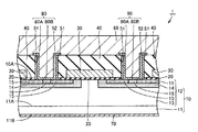
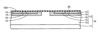
まず、本実施の形態に係る半導体装置としてのMOSFET1の構造について説明する。図1を参照して、MOSFET1は、炭化珪素からなる基板10と、ゲート絶縁膜20と、ゲート電極30と、層間絶縁膜40と、バッファ膜51と、ソース電極52と、ソース配線60と、ドレイン電極70とを備えている。基板10は、ベース基板11と、半導体層12とを含み、また半導体層12には、ドリフト領域13と、ボディ領域14と、ソース領域15と、コンタクト領域16とが形成されている。また、MOSFET1には、ゲート絶縁膜20と層間絶縁膜40とを貫通し、基板10の主表面10Aを露出させるコンタクトホール80がゲート電極30から離れて形成されている。
First, the structure of
ベース基板11は、たとえばN(窒素)等のn型不純物を含むことにより導電型がn型(第1導電型)となっている。ドリフト領域13は、ベース基板11の主表面11A上に形成されたエピタキシャル成長層である。ドリフト領域13は、ベース基板11と同様に、たとえばN(窒素)等のn型不純物を含むことにより導電型がn型となっており、その濃度はベース基板11よりも低くなっている。
ボディ領域14は、基板10の主表面10Aを含み、半導体層12内に互いに分離して形成されている。ボディ領域14は、たとえばAl(アルミニウム)やB(硼素)などのp型不純物を含むことにより、導電型がp型(第2導電型)となっている。
ソース領域15は、主表面10Aを含み、ボディ領域14に取り囲まれるように各々のボディ領域14内に形成されている。ソース領域15は、たとえばP(リン)などのn型不純物を含むことにより、ベース基板11およびドリフト領域13と同様に導電型がn型となっている。また、ソース領域15に含まれるn型不純物の濃度は、ドリフト領域13に含まれるn型不純物の濃度よりも高くなっている。
コンタクト領域16は、ソース領域15と同様に、主表面10Aを含みつつボディ領域14に取り囲まれ、かつソース領域15に隣接するように各々のボディ領域14内に形成されている。コンタクト領域16は、ボディ領域14と同様に、たとえばAl(アルミニウム)やB(硼素)などのp型不純物を含むことにより導電型がp型となっており、その濃度は、ボディ領域14よりも高くなっている。
Similar to source
ゲート絶縁膜20は、たとえばSiO2(二酸化珪素)からなり、主表面10A上に接触しつつ、一方のソース領域15の上面から他方のソース領域15の上面にまで延在するように形成されている。
ゲート電極30は、ゲート絶縁膜20上に接触しつつ、一方のソース領域15上から他方のソース領域15上にまで延在するように形成されている。ゲート電極30は、たとえば不純物が添加されたポリシリコンなどの導電体からなっている。
The
層間絶縁膜40は、たとえばSiO2(二酸化珪素)からなり、ゲート絶縁膜20上においてゲート電極30を取り囲むように形成されている。コンタクトホール80は、側壁面80Aと底面80Bとを有し、層間絶縁膜40およびゲート絶縁膜20を貫通して形成されている。また、図1に示すように、コンタクトホール80の側壁面80Aは層間絶縁膜40およびゲート絶縁膜20により構成され、また、底面80Bはソース領域15およびコンタクト領域16の上面となっている。
バッファ膜51は、コンタクトホール80内において、側壁面80A上に接触するように形成されている。また、バッファ膜51は、TiおよびNを含み、Alを含まない膜であって、たとえばTiNからなる膜であってもよい。また、バッファ膜51は、TiWからなる膜や、TaNからなる膜であってもよい。
The
ソース電極52は、バッファ膜51、およびコンタクトホール80を形成することにより露出した基板10の主表面10A上に接触するように形成されている。また、ソース電極52は、Ti、AlおよびSiを含む膜であって、たとえばTiAlSi合金からなっている。
ドレイン電極70は、ベース基板11の主表面11Aとは反対側の主表面11B上に形成されている。ドレイン電極70は、ソース電極52と同様に、たとえばTiAlSi合金からなっており、ベース基板11に対して電気的に接続されている。
The
ソース配線60は、ソース電極52および層間絶縁膜40を覆うように形成されている。ソース配線60は、たとえばAl(アルミニウム)等の金属からなっており、ソース電極52を介してソース領域15と電気的に接続されている。
The
次に、本実施の形態に係る半導体装置としてのMOSFET1の動作について説明する。図1を参照して、ゲート電極30に印加された電圧が閾値電圧未満の状態、すなわちオフ状態では、ソース電極52とドレイン電極70との間に電圧が印加されても、ボディ領域14とドリフト領域13との間に形成されるpn接合が逆バイアスとなり、非導通状態となる。一方、ゲート電極30に閾値電圧以上の電圧が印加されると、ボディ領域14に反転層が形成される。その結果、ソース領域15とドリフト領域13とが電気的に接続され、ソース電極52とドレイン電極70との間に電流が流れる。以上のようにして、MOSFET1は動作する。
Next, the operation of
以上のように、本実施の形態に係るMOSFET1では、ソース電極52は、層間絶縁膜40を貫通するコンタクトホール80の側壁面80Aに接触するように形成されたバッファ膜51上に接触するように形成されているため、ソース電極52と層間絶縁膜40との密着性を向上させることができる。このように、本実施の形態に係るMOSFET1は、アルミニウムを含む電極であるソース電極52と層間絶縁膜40との密着性を向上させることにより特性の安定した半導体装置となっている。
As described above, in
また、上述のように、MOSFET1において、バッファ膜51は、TiNからなっていてもよい。これにより、ソース電極52と層間絶縁膜40との密着性をより向上させることができる。
Further, as described above, in the
また、MOSFET1において、バッファ膜51は、0.025μm以上0.15μm以下の厚みを有していてもよい。このように、バッファ膜51の厚みは、ソース電極52と層間絶縁膜40との密着性を向上させるために必要な範囲内に設定することができる。
Further, in
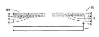
次に、本発明の一実施の形態に係る半導体装置の製造方法について、図1〜図15を参照して説明する。本実施の形態に係る半導体装置の製造方法においては、上記本実施の形態に係る半導体装置としてのMOSFET1が製造される。図2を参照して、まず、基板準備工程(S10)が実施される。この工程(S10)では、以下に説明する工程(S11)〜(S14)が実施されることにより、炭化珪素からなる基板10が準備される。
Next, a method for manufacturing a semiconductor device according to an embodiment of the present invention will be described with reference to FIGS. In the method for manufacturing a semiconductor device according to the present embodiment,
まず、工程(S11)として、ベース基板準備工程が実施される。この工程(S11)では、図5を参照して、たとえば4H−SiCからなるインゴット(図示しない)をスライスすることにより、導電型がn型のベース基板11が準備される。
First, as a step (S11), a base substrate preparation step is performed. In this step (S11), referring to FIG. 5, for example, an ingot (not shown) made of 4H—SiC is sliced to prepare
次に、工程(S12)として、エピタキシャル成長層形成工程が実施される。この工程(S12)では、図5を参照して、エピタキシャル成長により、ベース基板11の主表面11A上に導電型がn型の半導体層12が形成される。
Next, as a step (S12), an epitaxial growth layer forming step is performed. In this step (S <b> 12), referring to FIG. 5, n
次に、工程(S13)として、イオン注入工程が実施される。この工程(S13)では、図6を参照して、まず、たとえばAlイオンが、基板10の主表面10Aを含む領域に注入されることにより、半導体層12内に導電型がp型のボディ領域14が形成される。次に、たとえばPイオンが、上記Alイオンの注入深さよりも浅い深さでボディ領域14内に注入されることにより、導電型がn型のソース領域15が形成される。そして、たとえばAlイオンが、ボディ領域14内にさらに注入されることにより、ソース領域15と隣接し、かつソース領域15と同等の深さを有し、導電型がp型のコンタクト領域16が形成される。また、半導体層12において、ボディ領域14、ソース領域15およびコンタクト領域16のいずれも形成されない領域は、ドリフト領域13となる。
Next, as a step (S13), an ion implantation step is performed. In this step (S13), referring to FIG. 6, first, for example, Al ions are implanted into a region including
次に、工程(S14)として、活性化アニール工程が実施される。この工程(S14)では、基板10を加熱することにより、上記工程(S13)にて導入された不純物が活性化される。これにより、不純物が導入された領域において所望のキャリアが生成する。このようにして、上記工程(S11)〜(S14)が実施されることにより、不純物の導入により活性領域が形成された基板10が準備される。
Next, an activation annealing step is performed as a step (S14). In this step (S14), the impurities introduced in the step (S13) are activated by heating the
次に、工程(S20)として、ゲート絶縁膜形成工程が実施される。この工程(S20)では、図7を参照して、たとえば酸素を含む雰囲気中において基板10を加熱することにより、基板10の主表面10A上を覆うようにSiO2(二酸化珪素)からなるゲート絶縁膜20が形成される。
Next, as a step (S20), a gate insulating film forming step is performed. In this step (S20), referring to FIG. 7, for example, by
次に、工程(S30)として、ゲート電極形成工程が実施される。この工程(S30)では、図8を参照して、たとえばLPCVD(Low Pressure Chemical Vapor Deposition)法により、不純物を含むポリシリコンからなるゲート電極30がゲート絶縁膜20上に形成される。
Next, a gate electrode forming step is performed as a step (S30). In this step (S30), referring to FIG. 8,
次に、工程(S40)として、層間絶縁膜形成工程が実施される。この工程(S40)では、図9を参照して、たとえばP(Plasma)−CVD法により、SiO2(二酸化珪素)からなる層間絶縁膜40が、ゲート絶縁膜20とともにゲート電極30を取り囲むようにゲート絶縁膜20上に形成される。
Next, as a step (S40), an interlayer insulating film forming step is performed. In this step (S40), referring to FIG. 9,
次に、工程(S50)として、コンタクトホール形成工程が実施される。この工程(S50)では、図10を参照して、側壁面80Aおよび底面80Bを有し、基板10の主表面10Aを露出させるコンタクトホール80が形成される。具体的には、たとえばRIE(Reactive Ion Etching)などのエッチング方法を用いて、層間絶縁膜40およびゲート絶縁膜20を貫通するようにエッチングを進行させることにより、基板10の主表面10A(ソース領域15およびコンタクト領域16の上面)を露出させるコンタクトホール80が形成される。また、この工程(S50)では、コンタクトホール80は、ゲート電極30から離れて形成されるため、図10に示すようにゲート電極30がゲート絶縁膜20と層間絶縁膜40とにより取り囲まれた状態が維持される。
Next, as a step (S50), a contact hole forming step is performed. In this step (S50), referring to FIG. 10,
次に、工程(S60)として、バッファ膜形成工程が実施される。この工程(S60)では、図11を参照して、たとえばスパッタリングにより、コンタクトホール80の側壁面80Aおよび底面80B、ならびに層間絶縁膜40の上面上に接触するバッファ膜51が形成される。この工程(S60)では、TiおよびNを含み、Alを含まないバッファ膜51として、たとえばTiNからなる膜が形成されてもよい。また、バッファ膜51として、TiWからなる膜や、TaNからなる膜が形成されてもよい。また、この工程(S60)では、0.025μm以上0.15μm以下の厚みを有するバッファ膜51が形成されてもよい。
Next, as a step (S60), a buffer film forming step is performed. In this step (S60), referring to FIG. 11,
次に、工程(S70)として、エッチング工程が実施される。この工程(S70)では、図12中矢印に示すように、基板10の主表面10A側よりドライエッチングを実施することにより、層間絶縁膜40の上面およびコンタクトホール80の底面80B上に形成されたバッファ膜51が除去され、コンタクトホール80の側壁面80A上に形成されたバッファ膜51が残存する。
Next, an etching process is implemented as process (S70). In this step (S70), dry etching is performed from the
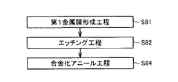
次に、工程(S80)として、オーミック電極形成工程が実施される。この工程(S80)では、図3および図4を参照して、以下に説明する工程(S81)〜(S84)が実施され、バッファ膜51、およびコンタクトホール80を形成することにより露出した基板10の主表面10A上に接触し、Ti、AlおよびSiを含むソース電極52と、ベース基板11の主表面11B上に接触し、たとえばソース電極52と同様の材料からなるドレイン電極70が形成される。
Next, an ohmic electrode forming step is performed as a step (S80). In this step (S80), with reference to FIG. 3 and FIG. 4, steps (S81) to (S84) described below are performed, and
まず、工程(S81)として、第1金属膜形成工程が実施される。この工程(S81)では、図13および図14を参照して、たとえばスパッタリングにより、Tiを含む第1金属層52aと、第1金属層52a上に接触しAlを含む第2金属層52bと、第2金属層52b上に接触しSiを含む第3金属層52cとが積層された構造を有する第1金属膜52dが形成される。また、この工程(S81)では、上述のように第1〜第3金属層52a〜52cが積層されることにより第1金属膜52dが形成されてもよいが、これに限られるものではない。たとえば、Ti、AlおよびSiを同時にスパッタリングすることにより、Ti、AlおよびSiが混合された第1金属膜52dが形成されてもよい。
First, as a step (S81), a first metal film forming step is performed. In this step (S81), referring to FIGS. 13 and 14, for example, by sputtering,
次に、工程(S82)として、エッチング工程が実施される。この工程(S82)では、コンタクトホール80の近傍にマスク(図示しない)を配置した上で、図15中矢印に示すように基板10の主表面10A側よりドライエッチングを実施することにより、層間絶縁膜40の上面に形成された第1金属膜52dが主に除去される。その結果、バッファ膜51、およびコンタクトホール80の底面80B上に接触して形成された第1金属膜52dが残存する。
Next, an etching process is implemented as process (S82). In this step (S82), a mask (not shown) is arranged in the vicinity of the
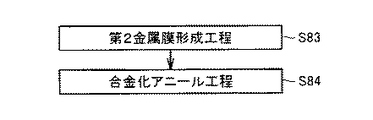
次に、工程(S83)として、第2金属膜形成工程が実施される。この工程(S83)では、図15を参照して、たとえばスパッタリングにより、ベース基板11の主表面11B上において、第1金属膜52dと同様に、Ti、AlおよびSiが積層または混合された第2金属膜70aが形成される。
Next, a second metal film forming step is performed as a step (S83). In this step (S83), referring to FIG. 15, the second layer in which Ti, Al, and Si are laminated or mixed on
次に、工程(S84)として、合金化アニール工程が実施される。この工程(S84)では、図1を参照して、上記工程(S81)および(S83)にて形成された第1および第2金属膜52d,70aが加熱される。これにより、第1および第2金属膜52d,70aを構成するTi、AlおよびSiの合金化が進行し、その結果TiAlSi合金からなり、基板10にオーミック接触するソース電極52およびドレイン電極70が形成される。このように、この工程(S80)では、工程(S81)、(S82)および(S84)が実施されることによりソース電極52が形成され(図3参照)、また工程(S83)および(S84)が実施されることによりドレイン電極70が形成される(図4参照)。
Next, an alloying annealing step is performed as a step (S84). In this step (S84), referring to FIG. 1, first and
次に、工程(S90)として、配線形成工程が実施される。この工程(S90)では、図1を参照して、たとえば蒸着法により、Alなどの導電体からなるソース配線60が、ソース電極50上に接触するように形成される。上記工程(S10)〜(S90)が実施されることにより、MOSFET1が製造され、本実施の形態に係る半導体装置の製造方法が完了する。
Next, as a step (S90), a wiring formation step is performed. In this step (S90), referring to FIG. 1,
以上のように、本実施の形態に係る半導体装置の製造方法では、層間絶縁膜40を貫通するコンタクトホール80の側壁面80A上に接触し、TiおよびNを含むバッファ膜51が形成された後に、バッファ膜51上に接触し、Ti、AlおよびSiを含むソース電極52が形成される。このように、本実施の形態に係る半導体装置の製造方法では、ソース電極52を形成する前にTiおよびNを含むバッファ膜51を予め形成することにより、ソース電極52と層間絶縁膜40との密着性を向上させることができる。したがって、本実施の形態に係る半導体装置の製造方法によれば、アルミニウムを含む電極であるソース電極52と層間絶縁膜40との密着性を向上させることにより特性の安定した上記本実施の形態に係る半導体装置としてのMOSFET1を製造することができる。
As described above, in the method of manufacturing a semiconductor device according to the present embodiment, after contacting the
また、上記本実施の形態において、ソース電極52は、これと同様にキャリア供給機能を有する電極であればよく、たとえばIGBTのエミッタ電極等を採用することができる。
Further, in the present embodiment, the
今回開示された実施の形態はすべての点で例示であって、制限的なものではないと考えられるべきである。本発明の範囲は上記した説明ではなく特許請求の範囲によって示され、特許請求の範囲と均等の意味、および範囲内でのすべての変更が含まれることが意図される。 The embodiment disclosed this time is to be considered as illustrative in all points and not restrictive. The scope of the present invention is defined by the terms of the claims, rather than the description above, and is intended to include any modifications within the scope and meaning equivalent to the terms of the claims.
本発明の半導体装置およびその製造方法は、アルミニウムを含む電極と層間絶縁膜との密着性を向上させることにより特性を安定化することが要求される半導体装置およびその製造方法において特に有利に適用され得る。 INDUSTRIAL APPLICABILITY The semiconductor device and the manufacturing method thereof according to the present invention are particularly advantageously applied to a semiconductor device and a manufacturing method thereof that require stabilization of characteristics by improving adhesion between an electrode containing aluminum and an interlayer insulating film. obtain.
1 MOSFET、10 基板、11 ベース基板、10A,11A,11B 主表面、12 半導体層、13 ドリフト領域、14 ボディ領域、15 ソース領域、16 コンタクト領域、20 ゲート絶縁膜、30 ゲート電極、40 層間絶縁膜、51 バッファ膜、52 ソース電極、52a 第1金属層、52b 第2金属層、52c 第3金属層、52d 第1金属膜、60 ソース配線、70 ドレイン電極、70a 第2金属膜、80 コンタクトホール、80A 側壁面、80B 底面。
1 MOSFET, 10 substrate, 11 base substrate, 10A, 11A, 11B main surface, 12 semiconductor layer, 13 drift region, 14 body region, 15 source region, 16 contact region, 20 gate insulating film, 30 gate electrode, 40
Claims (8)
前記基板の表面上に形成されたゲート絶縁膜と、
前記ゲート絶縁膜上に形成されたゲート電極と、
前記ゲート絶縁膜上において前記ゲート電極を取り囲むように形成された層間絶縁膜と、
TiおよびNを含み、Alを含まないバッファ膜と、
Ti、AlおよびSiを含むソース電極とを備え、
前記層間絶縁膜を貫通し、前記基板の前記表面を露出させるコンタクトホールが前記ゲート電極から離れて形成されており、
前記バッファ膜は、前記コンタクトホールの側壁面上に接触するように形成されており、
前記ソース電極は、前記コンタクトホールの側壁面上に接触する前記バッファ膜上に積層され、かつ、前記コンタクトホール内に位置する前記基板の前記表面上に接触する、半導体装置。 A substrate made of silicon carbide;
A gate insulating film formed on the surface of the substrate;
A gate electrode formed on the gate insulating film;
An interlayer insulating film formed on the gate insulating film so as to surround the gate electrode;
A buffer film containing Ti and N and no Al;
A source electrode containing Ti, Al and Si,
A contact hole penetrating the interlayer insulating film and exposing the surface of the substrate is formed away from the gate electrode;
The buffer film is formed in contact with the side wall surface of the contact hole,
The semiconductor device, wherein the source electrode is stacked on the buffer film in contact with a side wall surface of the contact hole, and is in contact with the surface of the substrate located in the contact hole .
前記基板の表面上にゲート絶縁膜を形成する工程と、
前記ゲート絶縁膜上にゲート電極を形成する工程と、
前記ゲート絶縁膜上に前記ゲート電極を取り囲む層間絶縁膜を形成する工程と、
前記層間絶縁膜を貫通し、前記基板の前記表面を露出させるコンタクトホールを前記ゲート電極から離れて形成する工程と、
前記コンタクトホールの側壁面上に接触し、TiおよびNを含み、Alを含まないバッファ膜を形成する工程と、
前記バッファ膜、およびコンタクトホールを形成することにより露出した前記基板の前記表面上に接触し、Ti、AlおよびSiを含むソース電極を形成する工程とを備える、半導体装置の製造方法。 Preparing a substrate made of silicon carbide;
Forming a gate insulating film on the surface of the substrate;
Forming a gate electrode on the gate insulating film;
Forming an interlayer insulating film surrounding the gate electrode on the gate insulating film;
Forming a contact hole penetrating the interlayer insulating film and exposing the surface of the substrate away from the gate electrode;
Forming a buffer film in contact with the side wall surface of the contact hole, containing Ti and N, and not containing Al;
Forming a source electrode containing Ti, Al, and Si in contact with the surface of the substrate exposed by forming the buffer film and a contact hole.
Tiを含む第1金属層と、前記第1金属層上に接触しAlを含む第2金属層と、前記第2金属層上に接触しSiを含む第3金属層とが積層された金属膜を形成する工程と、
前記金属膜を加熱することにより前記ソース電極を形成する工程とを含む、請求項4に記載の半導体装置の製造方法。 The step of forming the source electrode includes:
A metal film in which a first metal layer containing Ti, a second metal layer in contact with the first metal layer and containing Al, and a third metal layer in contact with the second metal layer and containing Si are stacked. Forming a step;
The method for manufacturing a semiconductor device according to claim 4, further comprising: forming the source electrode by heating the metal film.
Ti、AlおよびSiが混合された金属膜を形成する工程と、
前記金属膜を加熱することにより前記ソース電極を形成する工程とを含む、請求項4に記載の半導体装置の製造方法。 The step of forming the source electrode includes:
Forming a metal film in which Ti, Al and Si are mixed;
The method for manufacturing a semiconductor device according to claim 4, further comprising: forming the source electrode by heating the metal film.
Priority Applications (5)
| Application Number | Priority Date | Filing Date | Title |
|---|---|---|---|
| JP2012106022A JP5809596B2 (en) | 2012-05-07 | 2012-05-07 | Semiconductor device and manufacturing method thereof |
| PCT/JP2013/059491 WO2013168484A1 (en) | 2012-05-07 | 2013-03-29 | Semiconductor device and method for manufacturing same |
| CN201380015255.9A CN104170093B (en) | 2012-05-07 | 2013-03-29 | Semiconductor devices and its manufacturing method |
| EP13788394.8A EP2849231B1 (en) | 2012-05-07 | 2013-03-29 | Semiconductor device and method for manufacturing same |
| US13/856,950 US9177856B2 (en) | 2012-05-07 | 2013-04-04 | Semiconductor device and method for manufacturing same |
Applications Claiming Priority (1)
| Application Number | Priority Date | Filing Date | Title |
|---|---|---|---|
| JP2012106022A JP5809596B2 (en) | 2012-05-07 | 2012-05-07 | Semiconductor device and manufacturing method thereof |
Publications (2)
| Publication Number | Publication Date |
|---|---|
| JP2013235893A JP2013235893A (en) | 2013-11-21 |
| JP5809596B2 true JP5809596B2 (en) | 2015-11-11 |
Family
ID=49511866
Family Applications (1)
| Application Number | Title | Priority Date | Filing Date |
|---|---|---|---|
| JP2012106022A Active JP5809596B2 (en) | 2012-05-07 | 2012-05-07 | Semiconductor device and manufacturing method thereof |
Country Status (5)
| Country | Link |
|---|---|
| US (1) | US9177856B2 (en) |
| EP (1) | EP2849231B1 (en) |
| JP (1) | JP5809596B2 (en) |
| CN (1) | CN104170093B (en) |
| WO (1) | WO2013168484A1 (en) |
Families Citing this family (9)
| Publication number | Priority date | Publication date | Assignee | Title |
|---|---|---|---|---|
| JP2014038899A (en) | 2012-08-13 | 2014-02-27 | Sumitomo Electric Ind Ltd | Silicon carbide semiconductor device and method for manufacturing the same |
| JP5949305B2 (en) * | 2012-08-13 | 2016-07-06 | 住友電気工業株式会社 | Method for manufacturing silicon carbide semiconductor device |
| JP6068918B2 (en) | 2012-10-15 | 2017-01-25 | 住友電気工業株式会社 | Semiconductor device and manufacturing method thereof |
| JP6183200B2 (en) * | 2013-12-16 | 2017-08-23 | 住友電気工業株式会社 | Silicon carbide semiconductor device and manufacturing method thereof |
| JP6435686B2 (en) * | 2014-07-23 | 2018-12-12 | 富士電機株式会社 | Silicon carbide semiconductor device manufacturing method and silicon carbide semiconductor device |
| JP6191587B2 (en) * | 2014-12-08 | 2017-09-06 | トヨタ自動車株式会社 | Semiconductor device |
| CN109300947B (en) * | 2018-09-28 | 2021-09-07 | 京东方科技集团股份有限公司 | Flexible display substrate, manufacturing method thereof and display device |
| CN112823408A (en) * | 2018-10-08 | 2021-05-18 | 应用材料公司 | Method and apparatus for N-type metal oxide semiconductor (NMOS) metal gate material for Atomic Layer Deposition (ALD) processes using metal-based precursors |
| JP2021012996A (en) * | 2019-07-09 | 2021-02-04 | 株式会社豊田中央研究所 | Semiconductor device |
Family Cites Families (14)
| Publication number | Priority date | Publication date | Assignee | Title |
|---|---|---|---|---|
| JPH07202185A (en) * | 1993-12-28 | 1995-08-04 | Sharp Corp | Manufacture of vertical mos transistor |
| JP4003296B2 (en) | 1998-06-22 | 2007-11-07 | 株式会社デンソー | Silicon carbide semiconductor device and manufacturing method thereof |
| US6391785B1 (en) | 1999-08-24 | 2002-05-21 | Interuniversitair Microelektronica Centrum (Imec) | Method for bottomless deposition of barrier layers in integrated circuit metallization schemes |
| JP3559971B2 (en) | 2001-12-11 | 2004-09-02 | 日産自動車株式会社 | Silicon carbide semiconductor device and method of manufacturing the same |
| US20050087788A1 (en) | 2003-10-22 | 2005-04-28 | Matsushita Electric Industrial Co., Ltd. | Semiconductor device and method for fabricating the same |
| JP4002916B2 (en) * | 2003-10-22 | 2007-11-07 | 松下電器産業株式会社 | Semiconductor device and manufacturing method thereof |
| US8629490B2 (en) | 2006-03-31 | 2014-01-14 | Semiconductor Energy Laboratory Co., Ltd. | Nonvolatile semiconductor storage device with floating gate electrode and control gate electrode |
| CN101578705B (en) * | 2007-07-20 | 2012-05-30 | 松下电器产业株式会社 | Silicon carbide semiconductor device and method for manufacturing the same |
| JP5157843B2 (en) | 2007-12-04 | 2013-03-06 | 住友電気工業株式会社 | Silicon carbide semiconductor device and manufacturing method thereof |
| JP2010238738A (en) * | 2009-03-30 | 2010-10-21 | Toshiba Corp | Semiconductor device and method for manufacturing the semiconductor device |
| JP4858791B2 (en) * | 2009-05-22 | 2012-01-18 | 住友電気工業株式会社 | Semiconductor device and manufacturing method thereof |
| JP5860580B2 (en) * | 2009-05-25 | 2016-02-16 | 日産自動車株式会社 | Semiconductor device and manufacturing method thereof |
| JP5581642B2 (en) * | 2009-10-05 | 2014-09-03 | 住友電気工業株式会社 | Manufacturing method of semiconductor device |
| JP2013235895A (en) * | 2012-05-07 | 2013-11-21 | Sumitomo Electric Ind Ltd | Semiconductor device and method for manufacturing the same |
-
2012
- 2012-05-07 JP JP2012106022A patent/JP5809596B2/en active Active
-
2013
- 2013-03-29 CN CN201380015255.9A patent/CN104170093B/en active Active
- 2013-03-29 WO PCT/JP2013/059491 patent/WO2013168484A1/en active Application Filing
- 2013-03-29 EP EP13788394.8A patent/EP2849231B1/en active Active
- 2013-04-04 US US13/856,950 patent/US9177856B2/en active Active
Also Published As
| Publication number | Publication date |
|---|---|
| WO2013168484A1 (en) | 2013-11-14 |
| EP2849231A1 (en) | 2015-03-18 |
| EP2849231B1 (en) | 2019-10-30 |
| EP2849231A4 (en) | 2015-12-23 |
| US9177856B2 (en) | 2015-11-03 |
| US20130292703A1 (en) | 2013-11-07 |
| CN104170093A (en) | 2014-11-26 |
| JP2013235893A (en) | 2013-11-21 |
| CN104170093B (en) | 2018-06-01 |
Similar Documents
| Publication | Publication Date | Title |
|---|---|---|
| JP5809596B2 (en) | Semiconductor device and manufacturing method thereof | |
| JP5525940B2 (en) | Semiconductor device and manufacturing method of semiconductor device | |
| JP2013235895A (en) | Semiconductor device and method for manufacturing the same | |
| JP5708550B2 (en) | Silicon carbide semiconductor device and manufacturing method thereof | |
| KR20130109168A (en) | Method of manufacturing silicon carbide semiconductor device | |
| JP2009224365A (en) | Semiconductor device and method for fabricating the same | |
| WO2013088855A1 (en) | Method for manufacturing semiconductor device | |
| JP2015076592A (en) | Silicon carbide semiconductor device and manufacturing method of the same | |
| JP2014175470A (en) | Silicon carbide semiconductor device manufacturing method | |
| US9472635B2 (en) | Silicon carbide semiconductor device | |
| JP2011151350A (en) | Semiconductor device manufacturing method and the semiconductor device | |
| JPWO2012137412A1 (en) | Semiconductor device | |
| JP6068918B2 (en) | Semiconductor device and manufacturing method thereof | |
| JP2023080193A (en) | Manufacturing method of trench type semiconductor device | |
| JP2015201604A (en) | Silicon carbide semiconductor device and manufacturing method of the same | |
| JP2015204409A (en) | Silicon carbide semiconductor device and manufacturing method of the same | |
| JP5704003B2 (en) | Manufacturing method of semiconductor device | |
| JP2016143788A (en) | Manufacturing method of silicon carbide semiconductor device | |
| JP5721868B2 (en) | Semiconductor device and manufacturing method thereof | |
| JP2013093493A (en) | Semiconductor device manufacturing method | |
| JP6229443B2 (en) | Silicon carbide semiconductor device and manufacturing method thereof | |
| JP5991629B2 (en) | Semiconductor device and manufacturing method of semiconductor device |
Legal Events
| Date | Code | Title | Description |
|---|---|---|---|
| A621 | Written request for application examination |
Free format text: JAPANESE INTERMEDIATE CODE: A621 Effective date: 20150223 |
|
| A131 | Notification of reasons for refusal |
Free format text: JAPANESE INTERMEDIATE CODE: A131 Effective date: 20150602 |
|
| A521 | Request for written amendment filed |
Free format text: JAPANESE INTERMEDIATE CODE: A523 Effective date: 20150710 |
|
| TRDD | Decision of grant or rejection written | ||
| A01 | Written decision to grant a patent or to grant a registration (utility model) |
Free format text: JAPANESE INTERMEDIATE CODE: A01 Effective date: 20150825 |
|
| A61 | First payment of annual fees (during grant procedure) |
Free format text: JAPANESE INTERMEDIATE CODE: A61 Effective date: 20150911 |
|
| R150 | Certificate of patent or registration of utility model |
Ref document number: 5809596 Country of ref document: JP Free format text: JAPANESE INTERMEDIATE CODE: R150 |
|
| R250 | Receipt of annual fees |
Free format text: JAPANESE INTERMEDIATE CODE: R250 |
|
| R250 | Receipt of annual fees |
Free format text: JAPANESE INTERMEDIATE CODE: R250 |
|
| R250 | Receipt of annual fees |
Free format text: JAPANESE INTERMEDIATE CODE: R250 |
|
| R250 | Receipt of annual fees |
Free format text: JAPANESE INTERMEDIATE CODE: R250 |
|
| R250 | Receipt of annual fees |
Free format text: JAPANESE INTERMEDIATE CODE: R250 |
|
| R250 | Receipt of annual fees |
Free format text: JAPANESE INTERMEDIATE CODE: R250 |