JP5803550B2 - ANTENNA CIRCUIT, COMMUNICATION DEVICE, AND COMMUNICATION METHOD - Google Patents
ANTENNA CIRCUIT, COMMUNICATION DEVICE, AND COMMUNICATION METHOD Download PDFInfo
- Publication number
- JP5803550B2 JP5803550B2 JP2011226411A JP2011226411A JP5803550B2 JP 5803550 B2 JP5803550 B2 JP 5803550B2 JP 2011226411 A JP2011226411 A JP 2011226411A JP 2011226411 A JP2011226411 A JP 2011226411A JP 5803550 B2 JP5803550 B2 JP 5803550B2
- Authority
- JP
- Japan
- Prior art keywords
- capacitors
- circuit
- capacitor
- terminal
- communication
- Prior art date
- Legal status (The legal status is an assumption and is not a legal conclusion. Google has not performed a legal analysis and makes no representation as to the accuracy of the status listed.)
- Active
Links
- 238000004891 communication Methods 0.000 title claims description 161
- 238000000034 method Methods 0.000 title claims description 14
- 239000003990 capacitor Substances 0.000 claims description 300
- 230000005540 biological transmission Effects 0.000 claims description 69
- 239000003999 initiator Substances 0.000 description 20
- 230000008859 change Effects 0.000 description 18
- 230000007423 decrease Effects 0.000 description 10
- 238000006243 chemical reaction Methods 0.000 description 7
- 238000010586 diagram Methods 0.000 description 6
- 238000005516 engineering process Methods 0.000 description 5
- 230000005672 electromagnetic field Effects 0.000 description 4
- 230000008569 process Effects 0.000 description 4
- 230000015556 catabolic process Effects 0.000 description 2
- 238000006731 degradation reaction Methods 0.000 description 2
- 238000012986 modification Methods 0.000 description 2
- 230000004048 modification Effects 0.000 description 2
- 230000000087 stabilizing effect Effects 0.000 description 2
- 238000013459 approach Methods 0.000 description 1
- 230000000694 effects Effects 0.000 description 1
- 230000004044 response Effects 0.000 description 1
- 230000008054 signal transmission Effects 0.000 description 1
Images


Classifications
-
- H—ELECTRICITY
- H04—ELECTRIC COMMUNICATION TECHNIQUE
- H04B—TRANSMISSION
- H04B1/00—Details of transmission systems, not covered by a single one of groups H04B3/00 - H04B13/00; Details of transmission systems not characterised by the medium used for transmission
- H04B1/06—Receivers
- H04B1/16—Circuits
- H04B1/18—Input circuits, e.g. for coupling to an antenna or a transmission line
-
- H—ELECTRICITY
- H04—ELECTRIC COMMUNICATION TECHNIQUE
- H04B—TRANSMISSION
- H04B1/00—Details of transmission systems, not covered by a single one of groups H04B3/00 - H04B13/00; Details of transmission systems not characterised by the medium used for transmission
- H04B1/02—Transmitters
- H04B1/04—Circuits
- H04B1/0458—Arrangements for matching and coupling between power amplifier and antenna or between amplifying stages
Description
本開示は、アンテナ回路、通信装置、および通信方法に関し、特に、通信性能低下の改善を行うことができるようにしたアンテナ回路、通信装置、および通信方法に関する。 The present disclosure relates to an antenna circuit, a communication device, and a communication method, and more particularly, to an antenna circuit, a communication device, and a communication method that can improve communication performance degradation.
従来のリーダ/ライタは、非接触ICカードや携帯電話機からの信号を受信するとき、キャリア信号を非接触ICカードや携帯電話機に対して出力する。このキャリア信号に対して、非接触ICカードや携帯電話機が負荷変調を行うことにより、その変化量が、アンテナ回路のインピーダンスを調整する回路のある部分から取り出されて、リーダ/ライタの受信回路の受信端子に入力される。このようにして、非接触ICカードや携帯電話機からの信号の受信が行われていた(例えば、特許文献1参照)。 When a conventional reader / writer receives a signal from a non-contact IC card or a mobile phone, it outputs a carrier signal to the non-contact IC card or the mobile phone. When the non-contact IC card or mobile phone performs load modulation on this carrier signal, the amount of change is taken out from a portion of the circuit that adjusts the impedance of the antenna circuit, and the reception signal of the reader / writer Input to the receiving terminal. In this way, reception of signals from non-contact IC cards and mobile phones has been performed (see, for example, Patent Document 1).
ところで、受信回路に入力される信号品質は、非接触ICカードや携帯電話機と、リーダ/ライタのアンテナとの位置関係により変化する。この信号品質は、インピーダンス調整結果により決まり、カードの種類などによって異なる。リーダ/ライタの受信回路は、この信号を基に復号を行う。しかしながら、信号品質によっては復号が困難なことがあり、その結果、リーダ/ライタの通信距離低下や、一定の位置関係のときに通信性能が悪くなってしまう現象が発生することがあった。 By the way, the signal quality input to the receiving circuit varies depending on the positional relationship between the contactless IC card or mobile phone and the reader / writer antenna. This signal quality is determined by the impedance adjustment result and varies depending on the type of card. The receiving circuit of the reader / writer performs decoding based on this signal. However, depending on the signal quality, decoding may be difficult, and as a result, the communication distance of the reader / writer may be reduced, and the communication performance may deteriorate when the positional relationship is fixed.
一方、受信信号の品質がよくなるようなアンテナ調整を行うこともできるが、それを行うと、リーダ/ライタから磁界を効率よく出力することが困難になり、その結果、通信距離の低下を招く恐れがあった。 On the other hand, antenna adjustment can be performed so as to improve the quality of the received signal. However, if it is performed, it becomes difficult to efficiently output the magnetic field from the reader / writer, and as a result, the communication distance may be reduced. was there.
本開示は、このような状況に鑑みてなされたものであり、通信性能低下の改善を行うことができるものである。 This indication is made in view of such a situation, and can improve a communication performance fall.
本開示の一側面のアンテナ回路は、少なくとも第1および第2のコンデンサ、並びにアンテナコイルからなる共振回路と、送信端子と受信端子を有する送受信回路と、前記共振回路と前記送受信回路との間においてインピーダンスを調整する調整回路と、前記第1および第2のコンデンサの容量の組み合わせの設定値、および前記送受信回路が非接触で通信を行う対向する通信装置の通信特性と前記設定値とに関する情報を記憶する記憶部と、前記対向する通信装置の通信特性に応じて、前記第1および第2のコンデンサの容量の組み合わせの設定値を選択する制御部とを備え、前記第1および第2のコンデンサの容量の組み合わせは、前記第1および第2のコンデンサの合成容量の所定の範囲内において設定され、前記第1および第2のコンデンサの間に設けられる端子からの信号が、前記受信端子に入力され、前記第1および第2のコンデンサは、可変容量のダイオードであり、前記制御部は、選択した容量の組み合わせの設定値に基づいて、前記第1および第2のコンデンサの容量を設定する。 An antenna circuit according to an aspect of the present disclosure includes a resonance circuit including at least first and second capacitors and an antenna coil, a transmission / reception circuit having a transmission terminal and a reception terminal, and the resonance circuit and the transmission / reception circuit. Information regarding an adjustment circuit for adjusting impedance, a set value of a combination of the capacities of the first and second capacitors, and information on communication characteristics and the set value of a facing communication device in which the transmission / reception circuit performs contactless communication A storage unit for storing; and a control unit that selects a set value of a combination of the capacities of the first and second capacitors according to the communication characteristics of the opposing communication device , the first and second capacitors Is set within a predetermined range of the combined capacitance of the first and second capacitors, and the first and second capacitors are combined. Signal from the provided terminal between the capacitor is input to the reception terminal, the first and second capacitors, a diode of the variable capacitor, wherein the control unit, the set value of the combination of the capacitor selected Based on this, the capacitances of the first and second capacitors are set .
本開示の一側面の通信装置は、少なくとも第1および第2のコンデンサ、並びにアンテナコイルからなる共振回路と、送信端子と受信端子を有する送受信回路と、前記共振回路と前記送受信回路との間においてインピーダンスを調整する調整回路と、前記第1および第2のコンデンサの容量の組み合わせの設定値、および前記送受信回路が非接触で通信を行う対向する通信装置の通信特性と前記設定値とに関する情報を記憶する記憶部と、前記対向する通信装置の通信特性に応じて、前記第1および第2のコンデンサの容量の組み合わせの設定値を選択する制御部とを備え、前記第1および第2のコンデンサの容量の組み合わせは、前記第1および第2のコンデンサの合成容量の所定の範囲内において設定され、前記第1および第2のコンデンサの間に設けられる端子からの信号が、前記受信端子に入力され、前記第1および第2のコンデンサは、可変容量のダイオードであり、前記制御部は、選択した容量の組み合わせの設定値に基づいて、前記第1および第2のコンデンサの容量を設定するアンテナ回路を備える。 A communication device according to an aspect of the present disclosure includes a resonance circuit including at least first and second capacitors and an antenna coil, a transmission / reception circuit having a transmission terminal and a reception terminal, and the resonance circuit and the transmission / reception circuit. Information regarding an adjustment circuit for adjusting impedance, a set value of a combination of the capacities of the first and second capacitors, and information on communication characteristics and the set value of a facing communication device in which the transmission / reception circuit performs contactless communication A storage unit for storing; and a control unit that selects a set value of a combination of the capacities of the first and second capacitors according to the communication characteristics of the opposing communication device , the first and second capacitors Is set within a predetermined range of the combined capacitance of the first and second capacitors, and the first and second capacitors are combined. Signal from the provided terminal during service is input to the reception terminal, the first and second capacitors, a diode of the variable capacitor, wherein the control unit, the set value of the combination of the capacitor selected And an antenna circuit for setting the capacities of the first and second capacitors .
本開示の一側面においては、共振回路における第1および第2のコンデンサの容量の組み合わせが、前記第1および第2のコンデンサの合成容量の所定の範囲内において設定される。そして、前記第1および第2のコンデンサの間に設けられる端子からの信号が、受信端子に入力される。また、前記第1および第2のコンデンサは、可変容量のダイオードであり、対向する通信装置の通信特性に応じて選択された容量の組み合わせの設定値に基づいて、前記第1および第2のコンデンサの容量が設定される。 In one aspect of the present disclosure, a combination of the capacities of the first and second capacitors in the resonance circuit is set within a predetermined range of a combined capacity of the first and second capacitors. A signal from a terminal provided between the first and second capacitors is input to the receiving terminal. The first and second capacitors are variable capacitance diodes, and the first and second capacitors are set based on a set value of a combination of capacitors selected according to the communication characteristics of the opposing communication device. Capacity is set.
本開示の一側面においては、共振回路における第1および第2のコンデンサの容量の組み合わせが、前記第1および第2のコンデンサの合成容量の所定の範囲内において設定される。そして、前記第1および第2のコンデンサの間に設けられる端子からの信号が、受信端子に入力される。 In one aspect of the present disclosure, a combination of the capacities of the first and second capacitors in the resonance circuit is set within a predetermined range of a combined capacity of the first and second capacitors. A signal from a terminal provided between the first and second capacitors is input to the receiving terminal.
本開示の一側面によれば、通信することができる。特に、通信性能低下の改善を行うことができる。 According to one aspect of the present disclosure, communication is possible. In particular, communication performance degradation can be improved.
以下、本開示を実施するための形態(以下実施の形態とする)について説明する。なお、説明は以下の順序で行う。
1.第1の実施の形態(リーダ/ライタと非接触ICカードの通信システム)
2.第2の実施の形態(NFCデバイスの通信システム)
Hereinafter, modes for carrying out the present disclosure (hereinafter referred to as embodiments) will be described. The description will be given in the following order.
1. First embodiment (communication system of reader / writer and contactless IC card)
2. Second embodiment (communication system of NFC device)
<1.第1の実施の形態>
[従来のリーダ/ライタの回路構成例]
本開示との比較のため、図1を参照して、従来のリーダ/ライタの回路構成について説明する。図1は、従来のリーダ/ライタの回路構成例を示している。
<1. First Embodiment>
[Circuit configuration example of conventional reader / writer]
For comparison with the present disclosure, a circuit configuration of a conventional reader / writer will be described with reference to FIG. FIG. 1 shows a circuit configuration example of a conventional reader / writer.
従来のリーダ/ライタ1は、キャリア信号を、図示せぬ非接触ICカードに送信する。非接触ICカードは、負荷変調によりリーダ/ライタ1への返信を行うので、リーダ/ライタ1は、負荷変調による変化量を取得することで、非接触ICカードからの信号を受信する。
The conventional reader /
リーダ/ライタ1は、RF IC(Radio Frequency Integrated Circuit)11、コイルL1およびL2、コンデンサC1乃至C5、抵抗R1乃至R4、並びにアンテナコイル12などを含むように構成されている。
The reader /
RF IC11は、送信端子TX1およびTX2、接地用端子GND、受信端子RX、並びに中点電位端子VMIDを備えている。RF IC11は、図示せぬ送信回路と受信回路を有しており、送信端子TX1およびTX2は、送信回路から信号を出力する端子である。受信端子RXは、受信回路に信号を入力する端子である。
The
送信端子TX1およびTX2には、コイルL1およびL2の一端がそれぞれ接続されている。接地用端子GNDは接地されている。コイルL1の他端には、コンデンサC1の一端とコンデンサC3の一端が接続されている。コイルL2の他端には、コンデンサC2の一端とコンデンサC4の一端が接続されている。コンデンサC1の他端には、接地用端子GNDとコンデンサC2の他端が接続されている。 One ends of coils L1 and L2 are connected to the transmission terminals TX1 and TX2, respectively. The ground terminal GND is grounded. One end of a capacitor C1 and one end of a capacitor C3 are connected to the other end of the coil L1. One end of a capacitor C2 and one end of a capacitor C4 are connected to the other end of the coil L2. The other end of the capacitor C1 is connected to the ground terminal GND and the other end of the capacitor C2.
コイルL1およびL2は、コンデンサC1およびC2とともに、LPF(Low-Pass Filter)とインピーダンス変換の機能回路を構成している。 The coils L1 and L2 together with the capacitors C1 and C2 constitute an LPF (Low-Pass Filter) and a function circuit for impedance conversion.
コンデンサC3の他端は、抵抗R1を介して、アンテナコイル12の一端に直列接続されている。コンデンサC4の他端は、抵抗R2を介して、アンテナコイル12の他端に直列接続されている。コンデンサC3およびC4は、アンテナコイル12と共に共振回路を構成している。なお、コンデンサC1およびC2もその共振を補助している。
The other end of the capacitor C3 is connected in series to one end of the
抵抗R1およびR2は、その共振回路のQ Factor(品質係数)を調整する。 The resistors R1 and R2 adjust the Q factor (quality factor) of the resonance circuit.
RF IC11の受信端子RXは、コンデンサC4の一端、コンデンサC2の一端、およびコイルL2の他端が接続される交点に設けられた端子Zから、抵抗R3およびコンデンサC5を介して、信号を入力する。
The receiving terminal RX of the
抵抗R3は、端子Zからの信号のレベルが大きい場合、抵抗R4とともに分圧比を変えて、レベルを調整する処理を行っている。コンデンサC5は、端子Zからの信号(送信端子TX2からの信号)と、中点電位端子VMIDからの信号にある差を直流的にカットしている。 When the level of the signal from the terminal Z is large, the resistor R3 performs a process of adjusting the level by changing the voltage dividing ratio together with the resistor R4. The capacitor C5 cuts the difference between the signal from the terminal Z (signal from the transmission terminal TX2) and the signal from the midpoint potential terminal VMID in a DC manner.
中点電位端子VMIDは、コンデンサC6を介してアースされている。コンデンサC6は、中点電位を安定させるためのバイパスコンデンサである。中点電位端子VMIDは、中点電位を作って、その中点電位を抵抗R4を介して供給する。受信回路は、その中点電位端子VMIDの中点電位を基準として、受信端子RXから入力した信号を復号する。 The midpoint potential terminal VMID is grounded via a capacitor C6. The capacitor C6 is a bypass capacitor for stabilizing the midpoint potential. The midpoint potential terminal VMID generates a midpoint potential and supplies the midpoint potential via the resistor R4. The receiving circuit decodes the signal input from the receiving terminal RX with reference to the midpoint potential of the midpoint potential terminal VMID.
以上のように構成される従来のリーダ/ライタ1の受信回路に入力される信号品質は、インピーダンス調整の結果によって決まっていた。
The signal quality input to the receiving circuit of the conventional reader /
リーダ/ライタ1の受信回路は、受信端子RXから入力される信号を基に復号を行うが、信号品質によっては復号が困難なことがあり、その結果、リーダ/ライタ1の通信距離低下や一定の位置関係のときに通信性能が悪化することがあった。
The receiving circuit of the reader /
一方、受信信号の品質がよくなるように、アンテナ調整を行うと、リーダ/ライタ1から磁界を効率的に出力することができなくなってしまい、その結果、通信距離の低下が発生してしまっていた。
On the other hand, if the antenna is adjusted so that the quality of the received signal is improved, the magnetic field cannot be efficiently output from the reader /
そこで、本開示においては、リーダ/ライタから、非接触ICカードなどへの電力供給の特性を変化させることなく、返信信号の信号品質を変化させるようにする。以下に、詳細を説明していく。 Therefore, in the present disclosure, the signal quality of the return signal is changed without changing the characteristics of power supply from the reader / writer to the non-contact IC card or the like. Details will be described below.
[通信システムの構成例]
図2は、本開示を適用した通信システムの一実施の形態の構成を模式的に示すブロック図である。
[Configuration example of communication system]
FIG. 2 is a block diagram schematically illustrating a configuration of an embodiment of a communication system to which the present disclosure is applied.
図2に示される通信システム51は、リーダ/ライタ61と、対向する非接触ICカード62との間で非接触通信を行うシステムである。
A communication system 51 shown in FIG. 2 is a system that performs non-contact communication between a reader /
リーダ/ライタ61は、磁界を発生させる回路を有しており、磁界を発生させることにより、キャリア信号を非接触ICカード62に送信する。非接触ICカード62からの返信は、負荷変調方式で行われる。リーダ/ライタ61は、負荷変調による変化量を取得することで、非接触ICカード62からの信号を受信する。
The reader /
リーダ/ライタ61は、送信回路71、受信回路72、アンテナ調整回路73、並びに、コンデンサ74とアンテナコイル75からなる共振回路76を含むように構成されている。
The reader /
送信回路71は、対向する非接触ICカード62へキャリア信号の送信を行う。すなわち、送信回路71は、アンテナ調整回路73を介して、共振回路76に電流を流して電磁波を発生することにより、磁界を形成する。そして、送信回路71は、共振回路76が出力する搬送波としての電磁波を制御(変調)することにより、データを送信する。
The
受信回路72は、対向する非接触ICカード62からの信号の受信を行う。すなわち、受信回路72は、アンテナ調整回路73を介して、共振回路76からの電気信号を受信し、受信した信号を基に復号を行う。
The receiving
アンテナ調整回路73は、送信回路71および受信回路72と、共振回路76との間に設けられ、インピーダンスなどを調整して、非接触ICカード62からの返信信号を、受信回路72に入力する。
The
共振回路76は、コンデンサ74とアンテナコイル75とが並列に接続された共振型アンテナ回路である。この共振回路76の共振周波数が搬送波の周波数に対応し、共振回路76は、搬送波(電磁波)を出力する。また、共振回路76は、非接触ICカード62の共振回路86と結合し、結合された電磁場を電気信号に変換し、アンテナ調整回路73に供給する。
The
非接触ICカード62は、例えば、IC81、抵抗82、スイッチ83、並びに、コンデンサ84とアンテナコイル85からなる共振回路86により構成される。
The
IC81は、スイッチ83をオン、オフ動作することで、アンテナコイル85に対するインピーダンスの負荷を変動させる負荷変調方式により、対向するリーダ/ライタ61への信号の送信を制御する。
The
共振回路86は、コンデンサ84とアンテナコイル85とが並列に接続された共振型アンテナ回路である。共振回路86は、リーダ/ライタ61の共振回路76から放射された電磁場と結合し、結合された電磁場を電気信号に変換し、IC81などに供給する。
The
なお、図2の例においては、非接触ICカード62との通信システムの例を示したが、非接触ICカードに限らず、携帯電話機などであってもよい。
In the example of FIG. 2, an example of a communication system with the
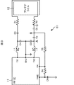
[リーダ/ライタの構成例]
図3は、リーダ/ライタの詳細な回路構成例を示している。
[Configuration example of reader / writer]
FIG. 3 shows a detailed circuit configuration example of the reader / writer.
図3に示されるリーダ/ライタ61は、RF IC(Radio Frequency Integrated Circuit)11、コイルL1およびL2、並びにコンデンサC1乃至C3を含むように構成されている。また、リーダ/ライタ61は、コンデンサCaおよびCb、コンデンサC6、抵抗R1乃至R4、並びにアンテナコイル12などを含むように構成されている。
The reader /
すなわち、リーダ/ライタ61は、RF IC11、コイルL1およびL2、コンデンサC1乃至C3、コンデンサC6、抵抗R1乃至R4、並びにアンテナコイル12を備える点が、図1のリーダ/ライタ1と共通している。
That is, the reader /
一方、リーダ/ライタ61は、コンデンサC4が、コンデンサCaおよびCbと入れ替わった点と、コンデンサC5が除かれた点が図1のリーダ/ライタ1と異なっている。
On the other hand, the reader /
RF IC11は、送信端子TX1およびTX2、接地用端子GND、受信端子RX、並びに中点電位端子VMIDを備えている。図3の例においては、図示されないが、RF IC11は、図2の送信回路71と受信回路72を有している。送信端子TX1およびTX2は、送信回路71から信号を出力する端子である。受信端子RXは、受信回路72に信号を入力する端子である。
The
送信端子TX1およびTX2には、コイルL1およびL2の一端がそれぞれ接続されている。接地用端子GNDは接地されている。コイルL1の他端には、コンデンサC1の一端とコンデンサC3の一端が接続されている。コイルL2の他端には、コンデンサC2の一端とコンデンサCaの一端が接続されている。コンデンサC1の他端には、接地用端子GNDとコンデンサC2の他端が接続されている。 One ends of coils L1 and L2 are connected to the transmission terminals TX1 and TX2, respectively. The ground terminal GND is grounded. One end of a capacitor C1 and one end of a capacitor C3 are connected to the other end of the coil L1. One end of a capacitor C2 and one end of a capacitor Ca are connected to the other end of the coil L2. The other end of the capacitor C1 is connected to the ground terminal GND and the other end of the capacitor C2.
コイルL1およびL2は、コンデンサC1およびC2とともに、LPF(Low-Pass Filter)とインピーダンス変換の機能を有する回路(すなわち、図2のアンテナ調整回路73に相当)である。
Coils L1 and L2, together with capacitors C1 and C2, are circuits having an LPF (Low-Pass Filter) and impedance conversion function (that is, corresponding to
コンデンサC3の他端は、抵抗R1を介して、アンテナコイル12の一端に直列接続されている。コンデンサCaの他端は、コンデンサCbの一端に接続されている。コンデンサCbの他端は、抵抗R2を介して、アンテナコイル12の他端に直列接続されている。すなわち、コンデンサCa、Cb、抵抗R2、アンテナコイル12の順に接続されている。
The other end of the capacitor C3 is connected in series to one end of the
コンデンサC3、Ca、およびCbは、アンテナコイル12と共振回路(すなわち、図2の共振回路76に相当)を構成している。なお、コンデンサC1およびC2もその共振を補助している。
Capacitors C3, Ca, and Cb constitute
抵抗R1およびR2は、共振回路のQ Factor(品質係数)を調整する。 Resistors R1 and R2 adjust the Q factor (quality factor) of the resonant circuit.
中点電位端子VMIDは、コンデンサC6を介してアースされている。中点電位端子VMIDは、中点電位を作って、その中点電位を抵抗R4を介して、受信端子RXに供給する。 The midpoint potential terminal VMID is grounded via a capacitor C6. The midpoint potential terminal VMID creates a midpoint potential and supplies the midpoint potential to the reception terminal RX via the resistor R4.
RFIC11の受信端子RXは、コンデンサCaおよびCbの間に示されるBのポイントに設けられる端子(以下、端子Bとも称する)から抵抗R3を介して、信号を入力する。すなわち、この場合、送信端子TX2からの信号が直接、受信端子RXに入力されないので、図1のコンデンサC5は必要ない。抵抗R3は、端子Bからの信号のレベルが大きい場合、抵抗R4とともに分圧比を変えて、レベルを調整する処理を行っている。
A receiving terminal RX of the
受信回路72は、中点電位端子VMIDの中点電位を基準として、受信端子RXから入力した信号を復号する。
The receiving
以上のように構成されるリーダ/ライタ61において、コンデンサCaおよびCbの合成容量は、図1のコンデンサC4と同じ値になるように調整される。これにより、リーダ/ライタ61の共振回路76から、従来のリーダ/ライタ1と同等の磁界の強さが出力される。
In the reader /
非接触ICカード62からの返信信号の波形は、図4および図5に示されるように、リーダ/ライタ61の共振回路76と非接触ICカード62の共振回路86との組み合わせや位置関係によって様々に変化する。
The waveform of the reply signal from the
図4および図5は、非接触ICカード62からの負荷変調の返信信号の波形の例を示している。
4 and 5 show examples of the waveform of the return signal of the load modulation from the
図4に示される返信信号の波形は、LレベルにおいてHレベルにおいても平らになっている部分がある。したがって、図4に示される波形の場合、リーダ/ライタ61の受信回路72において容易に復号可能である。
The waveform of the return signal shown in FIG. 4 has a portion that is flat at the L level and also at the H level. Therefore, the waveform shown in FIG. 4 can be easily decoded by the receiving
しかしながら、図5に示される返信信号の波形は、鋸波のようになっており、LレベルとHレベルとの変化点の判断が困難である。図5に示される波形の場合、リーダ/ライタ61の受信回路72で復号する際に、HレベルとLレベルのデューティー比が崩れてしまい、正確に復号することが困難である。
However, the waveform of the reply signal shown in FIG. 5 is a sawtooth wave, and it is difficult to determine the change point between the L level and the H level. In the case of the waveform shown in FIG. 5, when the
以上のことから、リーダ/ライタ61においては、非接触ICカード62からの返信信号の波形を受信回路72が受信しやすくなるように、図1のコンデンサC4と同じ値の範囲内で、コンデンサCaの容量とコンデンサCbの容量の組み合わせを変化させる。そして、コンデンサCaの容量とコンデンサCbの容量の組み合わせが、最適な受信波形となる組み合わせに設定される。これにより、最適な受信波形が受信回路72に入力されるようにすることができる。
From the above, in the reader /
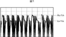
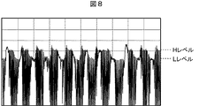
図6乃至図8は、図3のリーダ/ライタ61に示されるA、B、Cの各ポイントの返信信号の波形の例を示している。なお、図3の例においては、Aは、コイルL2の他端、コンデンサC2の一端、およびコンデンサCaの一端の交点である。Bは、コンデンサCaの他端とコンデンサCbの一端の間のポイントである。Cは、コンデンサCbの他端と抵抗R2の一端の間のポイントである。
6 to 8 show examples of return signal waveforms at points A, B, and C shown in the reader /
図6に示されるAのポイントの返信信号の波形は、図5の返信信号の波形と同様に、鋸波のようになっており、LレベルとHレベルとの変化点の判断が困難である。 The waveform of the return signal at point A shown in FIG. 6 is like a sawtooth wave, similar to the waveform of the return signal in FIG. 5, and it is difficult to determine the change point between the L level and the H level. .
図8に示されるCのポイントの返信信号の波形は、オーバーシュートが大きく出ており、この部分で受信回路72が正確に復号できない恐れがある。
The waveform of the return signal at point C shown in FIG. 8 has a large overshoot, and there is a possibility that the receiving
これらに対して、図7に示されるBのポイントの返信信号の波形は、図6および図7に示される波形の弱点を改善したような波形となっている。すなわち、図8に示される波形は、図6に示される波形に比して、HレベルおよびLレベルにおいて平らな部分があり、LレベルとHレベルの差もある。また、図8に示される波形は、図7に示される波形に比して、オーバーシュートがあまり出ていない。このため、受信回路72が復号しやすくなる。
On the other hand, the waveform of the return signal at point B shown in FIG. 7 is such that the weak points of the waveforms shown in FIGS. 6 and 7 are improved. That is, the waveform shown in FIG. 8 has flat portions at the H level and the L level as compared with the waveform shown in FIG. 6, and there is also a difference between the L level and the H level. Further, the waveform shown in FIG. 8 does not have much overshoot as compared with the waveform shown in FIG. For this reason, the receiving
したがって、Bのポイントに端子を設け、設けられた端子Bから、受信端子RXに信号を入力することで、よりよい波形の信号を受信端子RXに入力することができる。 Therefore, by providing a terminal at the point B and inputting a signal from the provided terminal B to the reception terminal RX, a signal having a better waveform can be input to the reception terminal RX.
図9は、リーダ/ライタ61において、コンデンサCaおよびCbの容量を変えた場合の非接触ICカード62との通信性能結果を示すグラフである。
FIG. 9 is a graph showing communication performance results with the
図9に示されるグラフにおいて、縦軸は、正答率[%]を表しており、横軸は通信距離[mm]を表している。コンデンサCaとCbの合成容量は、120〜123pFとして、図9の例においては、6種類のコンデンサCaの容量とCbの容量の組み合わせが示されている。 In the graph shown in FIG. 9, the vertical axis represents the correct answer rate [%], and the horizontal axis represents the communication distance [mm]. The combined capacitance of the capacitors Ca and Cb is 120 to 123 pF, and in the example of FIG. 9, combinations of six types of capacitors Ca and Cb are shown.
すなわち、上から順に、コンデンサCaをショートした時で、コンデンサCbが120pFの容量の組み合わせ、コンデンサCaが390pFの容量で、コンデンサCbが180pFの容量の組み合わせが示されている。また、コンデンサCaが270pFの容量で、コンデンサCbが220pFの容量の組み合わせ、コンデンサCaが220pFの容量で、コンデンサCbが270pFの容量の組み合わせが示されている。コンデンサCaが180pFの容量で、コンデンサCbが390pFの容量の組み合わせ、コンデンサCaが120pFの容量で、コンデンサCbをショートした時の組み合わせが示されている。 That is, in order from the top, when the capacitor Ca is short-circuited, the capacitor Cb has a capacitance combination of 120 pF, the capacitor Ca has a capacitance of 390 pF, and the capacitor Cb has a capacitance combination of 180 pF. Further, a combination of a capacitor Ca having a capacitance of 270 pF and a capacitor Cb having a capacitance of 220 pF, a capacitor Ca having a capacitance of 220 pF, and a capacitor Cb having a capacitance of 270 pF is shown. A combination of a capacitor Ca having a capacitance of 180 pF, a capacitor Cb having a capacitance of 390 pF, and a capacitor Ca having a capacitance of 120 pF and a short circuit of the capacitor Cb is shown.
コンデンサCaをショートした時で、コンデンサCbが120pFの容量の組み合わせの場合、正答率は、通信距離30mm前後で20%あたりまで落ちるが、33mm乃至37mmで100%になるものの、38mm前後で0%まで落ちている。なお、コンデンサCaとCbの合成容量が120〜123pFで、コンデンサCbが120pFということは、この結果が、従来のコンデンサC4を用いたリーダ/ライタ1の通信性能結果ともいえる。
When Capacitor Ca is shorted and Capacitor Cb is a combination of 120pF, the correct answer rate will drop to around 20% at a communication distance of around 30mm, but will be 100% at 33mm to 37mm, but will be 0% at around 38mm. Has fallen to. Note that the combined capacity of the capacitors Ca and Cb is 120 to 123 pF and the capacitor Cb is 120 pF. This result can be said to be the communication performance result of the reader /
コンデンサCaが390pFの容量で、コンデンサCbが180pFの容量の組み合わせの場合、正答率は、通信距離32mm前後で0%まで落ちるが、35mm乃至40mmで100%になるものの、43mm前後で0%まで落ちている。 When the capacitor Ca has a capacitance of 390 pF and the capacitor Cb has a capacitance of 180 pF, the correct answer rate drops to 0% at a communication distance of about 32 mm, but becomes 100% at 35 mm to 40 mm, but to about 0% at around 43 mm falling.
コンデンサCaが270pFの容量で、コンデンサCbが220pFの容量の組み合わせの場合、正答率は、通信距離40mm前後で90%まで落ちるが、42mmで100%になるものの、43mm前後で0%まで落ちている。 When the capacitor Ca has a capacitance of 270 pF and the capacitor Cb has a capacitance of 220 pF, the correct answer rate drops to 90% at a communication distance of about 40 mm, but drops to 100% at 42 mm, but drops to 0% at around 43 mm. Yes.
コンデンサCaが220pFの容量で、コンデンサCbが270pFの容量の組み合わせの場合、正答率は、通信距離40mm前後で0%まで落ちている。 When the capacitor Ca has a capacitance of 220 pF and the capacitor Cb has a capacitance of 270 pF, the correct answer rate drops to 0% at a communication distance of about 40 mm.
コンデンサCaが180pFの容量で、コンデンサCbが390pFの容量の組み合わせの場合、正答率は、通信距離30mm前後で0%まで落ちている。 When the capacitor Ca has a capacitance of 180 pF and the capacitor Cb has a capacitance of 390 pF, the correct answer rate drops to 0% at a communication distance of about 30 mm.
コンデンサCaが120pFの容量で、コンデンサCbをショートした時の組み合わせの場合、正答率は、通信距離36mm前後で30%まで落ちるが、37mmあたりで90%になるものの、39mm前後で20%まで落ちる。その後、正答率は、41mm前後で30%になるが、42mm前後で0%まで落ちている。 When the capacitor Ca is 120 pF and the capacitor Cb is short-circuited, the correct answer rate drops to 30% at a communication distance of around 36 mm, but drops to 90% at 37 mm, but drops to 20% at around 39 mm. . After that, the correct answer rate is 30% around 41mm, but it has dropped to 0% around 42mm.
このように容量の組み合わせによって、最大通信距離や正答率が低下するポイントが異なるが、この結果においては、コンデンサCaが270pFの容量で、コンデンサCbが220pFの容量の組み合わせのときが、一番通信性能がよくなっている。 As described above, the point at which the maximum communication distance and the correct answer rate decrease depends on the combination of the capacities, but in this result, the most communicative is when the capacitor Ca has a capacity of 270 pF and the capacitor Cb has a capacity of 220 pF. Performance is improving.
以上のように、リーダ/ライタにおいては、アンテナコイルと共振回路を構成し、アンテナコイルと直列に接続された複数のコンデンサの容量が、合成容量の所定の範囲内で、よりよい組み合わせに設定される。そして、容量が設定された複数のコンデンサの間にある端子から、受信回路への信号が取得される。これにより、返信信号の波形は、図4に示したような理想的な波形に近づき、結果、通信性能を向上させることができる。 As described above, in the reader / writer, an antenna coil and a resonance circuit are configured, and the capacities of a plurality of capacitors connected in series with the antenna coil are set to a better combination within a predetermined range of the combined capacity. The Then, a signal to the receiving circuit is obtained from a terminal between the plurality of capacitors having the set capacitance. Thereby, the waveform of the reply signal approaches an ideal waveform as shown in FIG. 4, and as a result, communication performance can be improved.
ところで、図2の通信システム51においては、非接触ICカード62から、リーダ/ライタ61に返信する負荷変調による返信信号の電圧レベルを任意に変化させることも可能である。
By the way, in the communication system 51 of FIG. 2, it is possible to arbitrarily change the voltage level of the reply signal by load modulation sent back from the
リーダ/ライタと、非接触ICカードのアンテナの位置を変化させると、負荷変調による返信信号の電圧レベルも変化し、ある位置で電圧レベルが非常に小さくなり、その結果、通信性能が悪化する位置が存在することがある。 When the position of the reader / writer and the antenna of the non-contact IC card is changed, the voltage level of the return signal due to load modulation also changes, and the voltage level becomes very small at a certain position, and as a result, the communication performance deteriorates. May exist.
図10は、リーダ/ライタ61において、コンデンサCaおよびCbの容量を変えた場合において、通信距離を変化させたときの負荷変調の電圧レベルを示すグラフである。
FIG. 10 is a graph showing voltage levels of load modulation when the communication distance is changed in the reader /
図10に示されるグラフにおいて、縦軸は、負荷変調レベル[mV]を表しており、横軸は通信距離[mm]を表している。コンデンサCaとCbの合成容量は、150〜165pFとして、図10の例においては、6種類のコンデンサCaの容量とCbの容量の組み合わせが示されている。 In the graph shown in FIG. 10, the vertical axis represents the load modulation level [mV], and the horizontal axis represents the communication distance [mm]. The combined capacitance of the capacitors Ca and Cb is 150 to 165 pF, and in the example of FIG. 10, combinations of six types of capacitors Ca and Cb are shown.
すなわち、上から順に、コンデンサCaをショートした時で、コンデンサCbが162pFの容量の組み合わせ、コンデンサCaが1000pFの容量で、コンデンサCbが180pFの容量の組み合わせが示されている。また、コンデンサCaが470pFの容量で、コンデンサCbが220pFの容量の組み合わせ、コンデンサCaが330pFの容量で、コンデンサCbが330pFの容量の組み合わせが示されている。コンデンサCaが220pFの容量で、コンデンサCbが470pFの容量の組み合わせ、コンデンサCaが180pFの容量で、コンデンサCbが1000pFの容量の組み合わせが示されている。 That is, in order from the top, when the capacitor Ca is short-circuited, the capacitor Cb has a combination of 162 pF, the capacitor Ca has a capacitance of 1000 pF, and the capacitor Cb has a combination of 180 pF. Further, a combination of a capacitor Ca having a capacitance of 470 pF, a capacitor Cb having a capacitance of 220 pF, a capacitor Ca having a capacitance of 330 pF, and a capacitor Cb having a capacitance of 330 pF is shown. A combination of a capacitor Ca having a capacitance of 220 pF, a capacitor Cb having a capacitance of 470 pF, a capacitor Ca having a capacitance of 180 pF, and a capacitor Cb having a capacitance of 1000 pF is shown.
コンデンサCaをショートした時で、コンデンサCbが162pFの容量の組み合わせの場合(すなわち、従来のリーダ/ライタ1の場合)、負荷変調レベルは、通信距離が2mm前後で18mVと高く、だんだん低くなり、14mm前後に2mVと低くなっている。 When the capacitor Ca is short-circuited and the capacitor Cb has a combination of 162 pF (ie, in the case of the conventional reader / writer 1), the load modulation level is as high as 18 mV when the communication distance is around 2 mm, and gradually decreases. It is as low as 2mV around 14mm.
コンデンサCaが1000pFの容量で、コンデンサCbが180pFの容量の組み合わせの場合、負荷変調レベルは、通信距離が0mm前後で14mVと高く、だんだん低くなり、10mm前後に2mVと低くなっている。また、負荷変調レベルは、通信距離が10mmからだんだん高くなり、18mmで7mVになってから、だんだん低くなっている。 When the capacitor Ca has a capacitance of 1000 pF and the capacitor Cb has a capacitance of 180 pF, the load modulation level is as high as 14 mV when the communication distance is around 0 mm, and gradually becomes low, and as low as 2 mV around 10 mm. Also, the load modulation level gradually increases from 10 mm for the communication distance, and gradually decreases after it reaches 7 mV at 18 mm.
コンデンサCaが470pFの容量で、コンデンサCbが220pFの容量の組み合わせの場合、負荷変調レベルは、通信距離が0mm前後に8mVで、だんだん低くなり、5mm前後に2mVと低くなっている。また、負荷変調レベルは、通信距離が5mmからだんだん高くなり、15mmで14mVになってから、だんだん低くなっている。 When the capacitor Ca has a capacitance of 470 pF and the capacitor Cb has a capacitance of 220 pF, the load modulation level is gradually reduced to 8 mV when the communication distance is around 0 mm, and is lowered to 2 mV around 5 mm. Also, the load modulation level gradually increases from a communication distance of 5 mm, and then decreases from 14 mV at 15 mm.
コンデンサCaが330pFの容量で、コンデンサCbが330pFの容量の組み合わせの場合、負荷変調レベルは、通信距離が0mm前後に5mVで、だんだん低くなり、4mm前後に3mVと低くなっている。また、負荷変調レベルは、通信距離が3mmからだんだん高くなり、12mmで16mVになってから、だんだん低くなっている。 When the capacitor Ca has a capacitance of 330 pF and the capacitor Cb has a capacitance of 330 pF, the load modulation level is gradually lowered to 5 mV when the communication distance is around 0 mm, and is lowered to 3 mV around 4 mm. In addition, the load modulation level gradually increases from 3 mm for the communication distance, and gradually decreases after it reaches 16 mV at 12 mm.
コンデンサCaが220pFの容量で、コンデンサCbが470pFの容量の組み合わせの場合、負荷変調レベルは、通信距離が0mm前後に3mVで、だんだん高くなり、10mm前後に15mVと高くなっている。また、負荷変調レベルは、通信距離が10mmからだんだん低くなっている。 When the capacitor Ca has a capacitance of 220 pF and the capacitor Cb has a capacitance of 470 pF, the load modulation level is gradually increased to 3 mV when the communication distance is around 0 mm, and is increased to 15 mV around 10 mm. In addition, the load modulation level gradually decreases from a communication distance of 10 mm.
コンデンサCaが180pFの容量で、コンデンサCbが1000pFの容量の組み合わせの場合、負荷変調レベルは、通信距離が0mm前後に7mVで、だんだん高くなり、9mm前後に19mVと高くなっている。また、負荷変調レベルは、通信距離が9mmからだんだん低くなっている。 When the capacitor Ca has a capacitance of 180 pF and the capacitor Cb has a capacitance of 1000 pF, the load modulation level is gradually increased to 7 mV when the communication distance is around 0 mm, and is increased to 19 mV around 9 mm. Also, the load modulation level gradually decreases from 9mm in communication distance.
以上のように、従来のリーダ/ライタ1においては、負荷変調レベルが非常に小さくなる通信距離の位置が存在する。これに対して、リーダ/ライタ61においては、コンデンサCaおよびCbの容量を変えると、負荷変調レベルが小さくなる位置が変化し、その位置が通信に影響があまりないようなコンデンサCaおよびCbの組み合わせが存在する。
As described above, in the conventional reader /
したがって、コンデンサCaおよびCbの複数の組み合わせのうち、負荷変調レベルが小さくなる位置が通信にあまり影響がないような組み合わせを選ぶことによって、安定して通信させたい距離における負荷変調レベルを大きくすることができる。その結果、通信システム51においては、通信性能を改善することができる。 Therefore, by selecting a combination of the capacitors Ca and Cb such that the position where the load modulation level becomes small does not affect the communication so much, the load modulation level at the distance to be stably communicated is increased. Can do. As a result, in the communication system 51, communication performance can be improved.
[リーダ/ライタの構成例]
図11は、リーダ/ライタの回路構成の他の例を示している。
[Configuration example of reader / writer]
FIG. 11 shows another example of the circuit configuration of the reader / writer.
図11に示されるリーダ/ライタ101は、RF IC11、コイルL1およびL2、コンデンサC1、コンデンサCaおよびCb、コンデンサC6、抵抗R1、R3、およびR4、並びにアンテナコイル12などを含むように構成されている。
A reader /
すなわち、リーダ/ライタ101は、アンテナ調整に使用する部品をできるだけ少なくした構成例で、コンデンサC2とC3、抵抗R2が除かれた点が、図3のリーダ/ライタ61と異なっている。
That is, the reader /
一方、リーダ/ライタ101は、RF IC11、コイルL1およびL2、コンデンサC1、コンデンサCaおよびCb、コンデンサC6、抵抗R1、R3、およびR4、並びにアンテナコイル12を備える点が図3のリーダ/ライタ61と共通している。なお、これらの共通している部分については、詳細な説明は繰り返しになるので適宜省略する。
On the other hand, the reader /
送信端子TX1およびTX2には、コイルL1およびL2の一端がそれぞれ接続されている。接地用端子GNDは接地されている。コイルL1の他端には、コンデンサC1の一端と抵抗R1の一端が接続されている。コイルL2の他端には、コンデンサC1の他端とコンデンサCaの一端が接続されている。 One ends of coils L1 and L2 are connected to the transmission terminals TX1 and TX2, respectively. The ground terminal GND is grounded. One end of a capacitor C1 and one end of a resistor R1 are connected to the other end of the coil L1. The other end of the capacitor C1 and one end of the capacitor Ca are connected to the other end of the coil L2.
コイルL1は、コンデンサC1とともに、LPFとインピーダンス変換の機能を有する回路(すなわち、図2のアンテナ調整回路73に相当)である。
The coil L1 is a circuit having a function of LPF and impedance conversion together with the capacitor C1 (that is, corresponding to the
抵抗R1は、アンテナコイル12の一端に直列接続されている。コンデンサCaの他端は、コンデンサCbの一端に接続されている。コンデンサCbの他端は、アンテナコイル12の他端に直列接続されている。すなわち、コンデンサCa、Cb、アンテナコイル12の順に接続されている。
The resistor R1 is connected in series to one end of the
コンデンサCaおよびCbと、アンテナコイル12とで共振回路(すなわち、図2の共振回路76に相当)を構成している。なお、コンデンサC1もその共振を補助している。
The capacitors Ca and Cb and the
RF IC11の受信端子RXは、コンデンサCaおよびCbの間に示されるDのポイントに設けられた端子(以下、端子Dとも称する)から抵抗R3を介して、信号を入力する。受信回路72は、中点電位端子VMIDの中点電位を基準として、受信端子RXから入力した信号を復号する。
The receiving terminal RX of the
以上のように構成されるリーダ/ライタ101においても、コンデンサCaおよびCbの容量を変化させて、合成容量の所定の範囲内でよりよい組み合わせが設定され、コンデンサCaおよびCbの間に設けられた端子Dから信号が受信端子RXに入力される。これにより、受信端子RXに入力される信号品質を変化させることが可能である。したがって、最適な受信波形を入力することができるので、通信性能の改善を行うことができる。
Also in the reader /
[リーダ/ライタの構成例]
図12は、リーダ/ライタの回路構成のさらに他の例を示している。
[Configuration example of reader / writer]
FIG. 12 shows still another example of the circuit configuration of the reader / writer.
図12に示されるリーダ/ライタ111は、RF IC11、コイルL1およびL2、コンデンサC1およびC2、コンデンサCaおよびCb、コンデンサC6、抵抗R1乃至R4、並びにアンテナコイル12などを含むように構成されている。
The reader /
すなわち、リーダ/ライタ111は、RF IC11、コイルL1およびL2、コンデンサC1およびC2、コンデンサCaおよびCb、コンデンサC6、抵抗R1乃至R4、並びにアンテナコイル12を備える点が図3のリーダ/ライタ61と共通している。なお、これらの共通している部分については、詳細な説明は繰り返しになるので適宜省略する。
That is, the reader /
一方、リーダ/ライタ111は、アンテナコイル12内に、コンデンサCaおよびCbが設けられた点と、コンデンサC3が除かれた点が図3のリーダ/ライタ61と異なっている。
On the other hand, the reader /
送信端子TX1およびTX2には、コイルL1およびL2の一端がそれぞれ接続されている。接地用端子GNDは接地されている。コイルL1の他端には、コンデンサC1の一端と抵抗R1の一端が接続されている。コイルL2の他端には、コンデンサC2の一端と抵抗R2の一端が接続されている。コンデンサC1の他端には、接地用端子GNDとコンデンサC2の他端が接続されている。 One ends of coils L1 and L2 are connected to the transmission terminals TX1 and TX2, respectively. The ground terminal GND is grounded. One end of a capacitor C1 and one end of a resistor R1 are connected to the other end of the coil L1. One end of a capacitor C2 and one end of a resistor R2 are connected to the other end of the coil L2. The other end of the capacitor C1 is connected to the ground terminal GND and the other end of the capacitor C2.
コイルL1およびL2は、コンデンサC1およびC2とともに、LPFとインピーダンス変換の機能を有する回路(すなわち、図2のアンテナ調整回路73に相当)である。
Coils L1 and L2, together with capacitors C1 and C2, are circuits having functions of LPF and impedance conversion (that is, equivalent to
抵抗R1の他端は、アンテナコイル12の一端に直列接続されている。抵抗R2の他端は、アンテナコイル12の他端に直列接続されている。
The other end of the resistor R1 is connected in series to one end of the
そして、リーダ/ライタ111においては、アンテナコイル12内(アンテナコイル12上)に、コンデンサCaおよびCbが設けられている。コンデンサCaおよびCbと、アンテナコイル12で共振回路(すなわち、図2の共振回路76に相当)を構成している。なお、コンデンサC1およびC2もその共振を補助している。
In the reader /
そして、アンテナコイル12内において、コンデンサCaとコンデンサCbの間に示されるEのポイントに設けられた端子(以下、端子Eとも称する)から、抵抗R3を介して、受信端子RXに信号が入力される。受信回路72は、中点電位端子VMIDの中点電位を基準として、受信端子RXから入力した信号を復号する。
In the
以上のように構成されるリーダ/ライタ111においても、コンデンサCaおよびCbの容量を変化させて、合成容量の所定の範囲内でよりよい組み合わせが設定される。そして、このように容量が設定されたコンデンサCaおよびCbの間に設けられた端子Eから信号が受信端子RXに入力される。これにより、受信端子RXに入力される信号品質を変化させることが可能である。したがって、最適な受信波形を入力することができるので、通信性能の改善を行うことができる。
Also in the reader /
[リーダ/ライタの構成例]
図13は、リーダ/ライタの回路構成のさらに他の例を示している。
[Configuration example of reader / writer]
FIG. 13 shows still another example of the circuit configuration of the reader / writer.
図13に示されるリーダ/ライタ121は、RF IC131、コイルL1およびL2、インダクタL3乃至L5、コンデンサC1乃至C6、抵抗R1乃至R4、並びにアンテナコイル12などを含むように構成されている。
The reader /
すなわち、リーダ/ライタ121は、コイルL1およびL2、コンデンサC1乃至C6、抵抗R1乃至R4、並びにアンテナコイル12を備える点が、図3のリーダ/ライタ61と共通している。なお、これらの共通している部分については、詳細な説明は繰り返しになるので適宜省略する。
That is, the reader /
一方、リーダ/ライタ121は、RF IC11がRF IC131と入れ替わった点、コンデンサCaおよびCbが、可変容量ダイオードD1およびD2に入れ替わった点、インダクタL3乃至L5が追加された点が、図3のリーダ/ライタ61と異なっている。
On the other hand, the reader /
RF IC131は、図示せぬ受信回路、送信回路の他に、マイクロコンピュータ141を内蔵している。RFIC131は、送信端子TX1およびTX2、接地用端子GND、受信端子RX、並びに中点電位端子VMIDの他に、マイクロコンピュータ141からの制御信号を、端子F乃至端子Hに送信する制御端子CTRL1乃至CTRL3を有している。
The
マイクロコンピュータ141は、制御端子CTRL1乃至CTRL3を介して、図3のコンデンサCaおよびCbに相当する可変容量ダイオードD1およびD2の容量を制御する。制御端子CTRL1乃至CTRL3は、任意の電位を出力可能な端子である。
The
送信端子TX1およびTX2には、コイルL1およびL2の一端がそれぞれ接続されている。接地用端子GNDは接地されている。コイルL1の他端には、コンデンサC1の一端とコンデンサC3の一端が接続されている。コイルL2の他端には、コンデンサC2の一端とコンデンサC4の一端が接続されている。コンデンサC1の他端には、接地用端子GNDとコンデンサC2の他端が接続されている。 One ends of coils L1 and L2 are connected to the transmission terminals TX1 and TX2, respectively. The ground terminal GND is grounded. One end of a capacitor C1 and one end of a capacitor C3 are connected to the other end of the coil L1. One end of a capacitor C2 and one end of a capacitor C4 are connected to the other end of the coil L2. The other end of the capacitor C1 is connected to the ground terminal GND and the other end of the capacitor C2.
コイルL1およびL2は、コンデンサC1およびC2とともに、LPFとインピーダンス変換の機能を有する回路(すなわち、図2のアンテナ調整回路73に相当)である。
Coils L1 and L2, together with capacitors C1 and C2, are circuits having functions of LPF and impedance conversion (that is, equivalent to
コンデンサC3の他端は、可変容量ダイオードD1の一端に接続されている。可変容量ダイオードD1の他端は、可変容量ダイオードD2の一端に接続されている。可変容量ダイオードD2の他端は、抵抗R1を介して、アンテナコイル12の一端に直列接続されている。すなわち、可変容量ダイオードD1、D2、抵抗R1、アンテナコイル12の順に接続されている。コンデンサC4の他端は、抵抗R2を介して、アンテナコイル12の他端に直列接続されている。
The other end of the capacitor C3 is connected to one end of the variable capacitance diode D1. The other end of the variable capacitance diode D1 is connected to one end of the variable capacitance diode D2. The other end of the variable capacitance diode D2 is connected in series to one end of the
そして、コンデンサC3の他端と可変容量ダイオードD1の一端の間には、制御端子CTRL1とインダクタL3を介して接続される端子Fが設けられている。可変容量ダイオードD1の他端と可変容量ダイオードD2の一端の間には、制御端子CTRL2とインダクタL4を介して接続される端子Gが設けられている。可変容量ダイオードD2の他端と抵抗R1の一端の間には、制御端子CTRL3とインダクタL5を介して接続される端子Hが設けられている。 A terminal F connected to the control terminal CTRL1 via an inductor L3 is provided between the other end of the capacitor C3 and one end of the variable capacitance diode D1. A terminal G connected to the control terminal CTRL2 via the inductor L4 is provided between the other end of the variable capacitance diode D1 and one end of the variable capacitance diode D2. A terminal H connected to the control terminal CTRL3 via an inductor L5 is provided between the other end of the variable capacitance diode D2 and one end of the resistor R1.
可変容量ダイオードD1およびD2は、電圧を逆方向に印加した場合にダイオードのPN接合の層の厚みが変化することによる、静電容量(接合容量)の変化を利用した可変容量コンデンサである。つまり、可変容量ダイオードD1およびD2は、逆バイアスを印加したときの両端の電位差により容量の値を可変にすることができる。 The variable capacitance diodes D1 and D2 are variable capacitance capacitors that utilize a change in capacitance (junction capacitance) due to a change in the thickness of the PN junction layer of the diode when a voltage is applied in the reverse direction. That is, the variable capacitance diodes D1 and D2 can change the capacitance value by the potential difference between both ends when a reverse bias is applied.
コンデンサC3は、可変容量ダイオードD1の電位を制御端子CTRL1から制御する任意の電位に設定するためのDC(直流成分)カット用コンデンサである。 The capacitor C3 is a DC (direct current component) cutting capacitor for setting the potential of the variable capacitance diode D1 to an arbitrary potential controlled from the control terminal CTRL1.
コンデンサC3、C4、可変容量ダイオードD1およびD2と、アンテナコイル12とで共振回路(すなわち、図2の共振回路76に相当)を構成している。なお、コンデンサC1およびC2もその共振を補助している。
The capacitors C3 and C4, the variable capacitance diodes D1 and D2, and the
インダクタL3乃至L5は、それぞれ、端子F乃至Hと各制御端子CTRL1乃至CTRL3を高周波的に分離するインダクタであり、アンテナ調整への影響を防止するための素子である。 The inductors L3 to L5 are inductors for separating the terminals F to H and the control terminals CTRL1 to CTRL3 at high frequencies, respectively, and are elements for preventing influence on antenna adjustment.
RFIC11の受信端子RXは、可変容量ダイオードD1およびD2の間に設けられた端子GからコンデンサC5および抵抗R3を介して、信号を入力する。受信回路72は、中点電位端子VMIDの中点電位を基準として、受信端子RXから入力した信号を復号する。
A reception terminal RX of the
以上のように構成されるリーダ/ライタ121において、マイクロコンピュータ141は、可変容量ダイオードD1およびD2の素子の個々の特性より、合計の容量を変化させないような条件の電位を、制御端子CTRL1乃至CTRL3から出力させる。
In the reader /
これにより、図3のリーダ/ライタ61と同様の機能を有することができる。すなわち、非接触ICカード62からの返信信号の波形を受信回路が受信しやすくなるように、図1のコンデンサC4と同じ値の範囲(所定の範囲)内で、可変容量ダイオードD1およびD2の素子の容量の組み合わせを制御し、変化させることができる。
Thereby, it can have the same function as the reader /
さらに、マイクロコンピュータ141は、可変容量ダイオードD1およびD2に対して、各コンデンサの容量の組み合わせの設定値を複数のパターンを、内蔵する記憶部に記憶しておく。また、マイクロコンピュータ141は、対向する非接触ICカードや携帯電話機の特性に応じた最適な組み合わせの設定値に関する情報を記憶部に記憶する。そして、マイクロコンピュータ141は、RF IC131の、図示せぬ受信回路および送信回路を用いての通信を行うことで、対向する非接触ICカードや携帯電話機の通信特性を検出し、検出された通信特性に応じて最適な設定を選択する。マイクロコンピュータ141は、選択した最適な設定値となるような条件の電位を、制御端子CTRL1乃至CTRL3から出力させ、可変容量ダイオードD1およびD2の素子の容量を変化させる。
Further, the
これにより、可変容量ダイオードD1およびD2の容量のよりよい組み合わせが設定され、可変容量ダイオードD1およびD2の間に設けられた端子Gから信号が受信端子RXに入力される。その結果、対向する非接触ICカードや携帯電話機の通信特性に応じた最適な受信波形が、リーダ/ライタ121の受信回路に入力される。したがって、非接触ICカードや携帯電話機などの通信特性がそれぞれ異なる機器と通信を行う環境下において、通信性能を担保して好適な通信を行うことができる。
Thereby, a better combination of the capacitances of the variable capacitance diodes D1 and D2 is set, and a signal is input from the terminal G provided between the variable capacitance diodes D1 and D2 to the reception terminal RX. As a result, an optimal reception waveform corresponding to the communication characteristics of the opposed non-contact IC card or mobile phone is input to the reception circuit of the reader /
以上より、様々な種類の非接触ICカードや携帯電話機に対する通信性能改善を容易に行うことができる。 As described above, it is possible to easily improve communication performance for various types of non-contact IC cards and mobile phones.
<2.第2の実施の形態>
[従来の通信システムの構成例]
本開示との比較のため、図14を参照して、従来の通信システムについて説明する。図14は、従来の通信システムの構成例を示している。
<2. Second Embodiment>
[Configuration example of conventional communication system]
For comparison with the present disclosure, a conventional communication system will be described with reference to FIG. FIG. 14 shows a configuration example of a conventional communication system.
図14に示される通信システム151は、NFC(Near Field Communication)デバイスであるイニシエータ161とターゲット162との間において、passive communication modeで非接触通信を行うシステムである。 A communication system 151 shown in FIG. 14 is a system that performs contactless communication in an passive communication mode between an initiator 161 and a target 162, which are NFC (Near Field Communication) devices.
図14の例において、イニシエータ161およびターゲット162は、図1のリーダ/ライタ1と同様に、磁界を発生させる回路を有しており、磁界を発生させることにより、キャリア信号を相手に送信することができる。また、イニシエータ161およびターゲット162は、図示せぬ非接触ICカードと同様に、キャリア信号を送ってきた相手に対する返信を負荷変調方式で行う。
In the example of FIG. 14, the initiator 161 and the target 162 have a circuit that generates a magnetic field, like the reader /
つまり、イニシエータ161およびターゲット162は、それぞれ、図1のリーダ/ライタ1にもなりうるし、図示せぬ非接触ICカードにもなりうる。
That is, the initiator 161 and the target 162 can each be the reader /
イニシエータ161およびターゲット162は、図1の従来のリーダ/ライタ1と基本的に同様に構成される。すなわち、イニシエータ161およびターゲット162は、それぞれ、コイルL1およびL2、コンデンサC1乃至C6、抵抗R1乃至R4、RFIC11、並びにアンテナコイル12を備えている。
The initiator 161 and the target 162 are basically configured similarly to the conventional reader /
したがって、RF IC11は、送信端子TX1およびTX2、接地用端子GND、受信端子RX、並びに中点電位端子VMIDを備えている。なお、図1のRFIC11の例においては省略されていたが、図14のRF IC11においては、送信端子TX1と接地用端子GNDとを接続するスイッチS1と、送信端子TX2と接地用端子GNDとを接続するスイッチS2とが示されている。
Therefore, the
送信端子TX1およびTX2には、コイルL1およびL2の一端がそれぞれ接続されている。接地用端子GNDは接地されている。コイルL1の他端には、コンデンサC1の一端とコンデンサC3の一端が接続されている。コイルL2の他端には、コンデンサC2の一端とコンデンサC4の一端が接続されている。コンデンサC1の他端には、接地用端子GNDとコンデンサC2の他端が接続されている。 One ends of coils L1 and L2 are connected to the transmission terminals TX1 and TX2, respectively. The ground terminal GND is grounded. One end of a capacitor C1 and one end of a capacitor C3 are connected to the other end of the coil L1. One end of a capacitor C2 and one end of a capacitor C4 are connected to the other end of the coil L2. The other end of the capacitor C1 is connected to the ground terminal GND and the other end of the capacitor C2.
コイルL1およびL2、コンデンサC1およびC2とともに、LPF(Low-Pass Filter)とインピーダンス変換の機能回路を構成している。 Together with the coils L1 and L2 and the capacitors C1 and C2, a functional circuit for LPF (Low-Pass Filter) and impedance conversion is configured.
コンデンサC3の他端は、抵抗R1を介して、アンテナコイル12の一端に直列接続されている。コンデンサC4の他端は、抵抗R2を介して、アンテナコイル12の他端に直列接続されている。コンデンサC3およびC4と、アンテナコイル12とで共振回路を構成している。なお、コンデンサC1およびC2もその共振を補助している。
The other end of the capacitor C3 is connected in series to one end of the
抵抗R1およびR2は、共振回路のQ Factor(品質係数)を調整する。 Resistors R1 and R2 adjust the Q factor (quality factor) of the resonant circuit.
RF IC11の受信端子RXは、コンデンサC4の一端、コンデンサC2の一端、およびコイルL2の他端が接続される交点の端子Pから、抵抗R3およびコンデンサC5を介して、信号を入力する。入力される信号は、中点電位をクロスする。受信回路は、中点電位端子VMIDの中点電位を基準として、受信端子RXから入力した信号を復号する。
The reception terminal RX of the
抵抗R3は、端子Pからの信号のレベルが大きい場合、抵抗R4とともに分圧比を変えて、レベルを調整する処理を行っている。コンデンサC5は、端子Pからの信号(送信端子TX2からの信号)と、中点電位端子VMIDからの信号にある差を直流的にカットしている。 When the level of the signal from the terminal P is large, the resistor R3 performs a process of adjusting the level by changing the voltage dividing ratio together with the resistor R4. The capacitor C5 cuts the difference between the signal from the terminal P (signal from the transmission terminal TX2) and the signal from the midpoint potential terminal VMID in a DC manner.
中点電位端子VMIDは、コンデンサC6を介してアースされている。コンデンサC6は、中点電位を安定させるためのバイパスコンデンサである。中点電位端子VMIDは、中点電位を作って、抵抗R4を介して供給する。 The midpoint potential terminal VMID is grounded via a capacitor C6. The capacitor C6 is a bypass capacitor for stabilizing the midpoint potential. The midpoint potential terminal VMID generates a midpoint potential and supplies it through the resistor R4.
このような通信システム151において、例えば、ターゲット162は、イニシエータ161に対して返信を行う場合、スイッチS1およびS2のオン/オフにより、送信端子TX1およびTX2を接地用端子GNDと接続することで、負荷変調を行う。 In such a communication system 151, for example, when the target 162 sends a reply to the initiator 161, the transmission terminals TX1 and TX2 are connected to the ground terminal GND by turning on and off the switches S1 and S2. Perform load modulation.
しかしながら、このスイッチS1およびS2のオン/オフにより、送信端子TX1およびTX2のDCレベルが変化し、その変化の影響を受けて、端子PのDCレベルも変化する。 However, the DC levels of the transmission terminals TX1 and TX2 change due to the on / off of the switches S1 and S2, and the DC level of the terminal P also changes under the influence of the change.
この結果、受信端子RXのDCレベルが変化し、受信端子RXに入力するキャリア信号の中点電位が変化するため、図15に示されるように、キャリア信号が中点電位をクロスしないことが発生してしまう。このような場合、イニシエータ161のRFIC11の受信回路は、クロックを正確にカウントできない。このため、ターゲット162からイニシエータ161への返信時にパケットの長さが、本来の長さより長くなってしまうので、通信に失敗してしまう。
As a result, the DC level of the receiving terminal RX changes and the midpoint potential of the carrier signal input to the receiving terminal RX changes, so that the carrier signal does not cross the midpoint potential as shown in FIG. Resulting in. In such a case, the receiving circuit of the
図15は、従来の通信システム151におけるキャリア信号の波形を示している。すなわち、図15の例においては、従来の通信システム151において、パケットの長さが本来の長さより長くなってしまっているときのキャリア信号の波形が示されている。 FIG. 15 shows the waveform of the carrier signal in the conventional communication system 151. That is, in the example of FIG. 15, in the conventional communication system 151, the waveform of the carrier signal when the packet length is longer than the original length is shown.
図15の波形においては、Qが付された丸に示されるように、キャリア信号が中点電位をクロスしない部分が発生してしまっている。イニシエータ161のRFIC11の受信回路は、図15のQが示される丸に囲まれた部分のクロックを、カウントすることが困難である。
In the waveform of FIG. 15, as indicated by a circle with Q, there is a portion where the carrier signal does not cross the midpoint potential. It is difficult for the receiving circuit of the
[本技術の通信システムの構成例]
図16は、本技術を適用した通信システムの構成例を示している。
[Configuration example of the communication system of the present technology]
FIG. 16 illustrates a configuration example of a communication system to which the present technology is applied.
図16に示される通信システム201は、NFCデバイスであるイニシエータ211とターゲット212との間において、passive communication modeで非接触通信を行うシステムである。 A communication system 201 illustrated in FIG. 16 is a system that performs non-contact communication in an passive communication mode between an initiator 211 and a target 212 that are NFC devices.
図16の例において、イニシエータ211およびターゲット212は、図2のリーダ/ライタ61と同様に、磁界を発生させる回路を有しており、磁界を発生させることにより、キャリア信号を相手に送信することができる。また、イニシエータ211およびターゲット212は、図2の非接触ICカード62と同様に、キャリア信号を送ってきた相手に対する返信を負荷変調方式で行う。
In the example of FIG. 16, the initiator 211 and the target 212 have a circuit that generates a magnetic field, like the reader /
つまり、イニシエータ211およびターゲット212は、それぞれ、図2のリーダ/ライタ61にもなりうるし、図2の非接触ICカード62にもなりうる。
That is, the initiator 211 and the target 212 can each be the reader /
イニシエータ211およびターゲット212は、基本的に、図3のリーダ/ライタ61と同様に構成される。すなわち、イニシエータ211およびターゲット212は、コイルL1およびL2、コンデンサC1乃至C3、コンデンサCaおよびCb、コンデンサC6、抵抗R1乃至R4、RF IC11、並びにアンテナコイル12を備えている。
The initiator 211 and the target 212 are basically configured similarly to the reader /
RF IC11は、図示されないが、送信回路と受信回路を有しており、送信端子TX1およびTX2、接地用端子GND、受信端子RX、並びに中点電位端子VMIDを備えている。送信端子TX1およびTX2は、送信回路から信号を出力する端子である。受信端子RXは、受信回路に信号を入力する端子である。なお、図3のRFIC11の例においては省略されていたが、図16のRF IC11においては、送信端子TX1と接地用端子GNDとを接続するスイッチS1と、送信端子TX2と接地用端子GNDとを接続するスイッチS2とが示されている。
Although not shown, the
送信端子TX1およびTX2には、コイルL1およびL2の一端がそれぞれ接続されている。接地用端子GNDは接地されている。コイルL1の他端には、コンデンサC1の一端とコンデンサC3の一端が接続されている。コイルL2の他端には、コンデンサC2の一端とコンデンサCaの一端が接続されている。コンデンサC1の他端には、接地用端子GNDとコンデンサC2の他端が接続されている。 One ends of coils L1 and L2 are connected to the transmission terminals TX1 and TX2, respectively. The ground terminal GND is grounded. One end of a capacitor C1 and one end of a capacitor C3 are connected to the other end of the coil L1. One end of a capacitor C2 and one end of a capacitor Ca are connected to the other end of the coil L2. The other end of the capacitor C1 is connected to the ground terminal GND and the other end of the capacitor C2.
コイルL1およびL2は、コンデンサC1およびC2とともに、LPFとインピーダンス変換の機能を有する回路(すなわち、図2のアンテナ調整回路73に相当)である。
Coils L1 and L2, together with capacitors C1 and C2, are circuits having functions of LPF and impedance conversion (that is, equivalent to
コンデンサC3の他端は、抵抗R1を介して、アンテナコイル12の一端に直列接続されている。コンデンサCaの他端は、コンデンサCbの一端に接続されている。コンデンサCbの他端は、抵抗R2を介して、アンテナコイル12の他端に直列接続されている。すなわち、コンデンサCa、Cb、抵抗R2、アンテナコイル12の順に接続されている。
The other end of the capacitor C3 is connected in series to one end of the
コンデンサC3、Ca、およびCbと、アンテナコイル12とで共振回路(すなわち、図2の共振回路76に相当)を構成している。なお、コンデンサC1およびC2もその共振を補助している。
Capacitors C3, Ca, and Cb and
抵抗R1およびR2は、共振回路のQ Factor(品質係数)を調整する。 Resistors R1 and R2 adjust the Q factor (quality factor) of the resonant circuit.
中点電位端子VMIDは、コンデンサC6を介してアースされている。中点電位端子VMIDは、中点電位を作って、中点電位を抵抗R4を介して、受信端子RXに供給する。 The midpoint potential terminal VMID is grounded via a capacitor C6. The midpoint potential terminal VMID creates a midpoint potential and supplies the midpoint potential to the reception terminal RX via the resistor R4.
RF IC11の受信端子RXは、コンデンサCaおよびCbの間に示されるポイントRに設けられた端子(以下、端子Rとも称する)から抵抗R3を介して、信号を入力する。抵抗R3は、端子Rからの信号のレベルが大きい場合、抵抗R4とともに分圧比を変えて、レベルを調整する処理を行っている。
The reception terminal RX of the
受信回路72は、中点電位端子VMIDの中点電位を基準にして、受信端子RXから入力した信号を復号する。
The
このような通信システム201において、例えば、ターゲット212は、イニシエータ211に対して返信を行う場合、スイッチS1およびS2のオン/オフにより、送信端子TX1およびTX2を接地用端子GNDと接続することで、負荷変調を行う。 In such a communication system 201, for example, when the target 212 sends a reply to the initiator 211, by connecting the transmission terminals TX1 and TX2 to the ground terminal GND by turning on and off the switches S1 and S2, Perform load modulation.
このスイッチS1およびS2のオン/オフにより、送信端子TX1およびTX2のDCレベルが変化し、その変化の影響を受けて、Pで示されるポイントのDCレベルも変化する。そこで、ターゲット212においては、コンデンサCaが備えられていることにより、端子Rにおいて、送信端子TX1およびTX2のDCレベルの変化の影響が低減される。 By turning on / off the switches S1 and S2, the DC levels of the transmission terminals TX1 and TX2 change. Under the influence of the change, the DC level at the point indicated by P also changes. Therefore, the target 212 is provided with the capacitor Ca, so that the influence of the change in the DC level of the transmission terminals TX1 and TX2 is reduced at the terminal R.
これにより、イニシエータ211においては、受信端子RXに入力されるキャリア信号のクロックを正確にカウントすることができ、パケットの長さが長くなるような通信での不具合の発生を抑制することができる。 Thereby, in the initiator 211, the clock of the carrier signal input to the receiving terminal RX can be accurately counted, and the occurrence of troubles in communication that increases the packet length can be suppressed.
図17は、従来の通信システムと本技術の通信システムによる通信性能結果を示す図である。 FIG. 17 is a diagram illustrating communication performance results obtained by the conventional communication system and the communication system of the present technology.
図17の例において、横軸は、通信距離[mm]を表しており、縦軸は、正答率[%]を表している。 In the example of FIG. 17, the horizontal axis represents the communication distance [mm], and the vertical axis represents the correct answer rate [%].
従来の通信システム151の正答率は、通信距離が0乃至6mmのところで0%である。従来の通信システム151の正答率は、通信距離が6乃至10mmにかけて、100%までだんだん上がっている。そして、従来の通信システム151の正答率は、通信距離が20乃至36mmにかけて、0%までだんだん下がっている。 The correct answer rate of the conventional communication system 151 is 0% when the communication distance is 0 to 6 mm. The accuracy rate of the conventional communication system 151 gradually increases to 100% over a communication distance of 6 to 10 mm. The accuracy rate of the conventional communication system 151 gradually decreases to 0% over a communication distance of 20 to 36 mm.
これに対して、本技術の通信システム201の正答率は、通信距離が0乃至37mmのところで100%であるが、38mmのところで急激に下がる。 On the other hand, the correct answer rate of the communication system 201 of the present technology is 100% when the communication distance is 0 to 37 mm, but rapidly decreases when the communication distance is 38 mm.
すなわち、従来の通信システム151の場合、近接付近と遠方において通信性能が悪化しているが、本技術の通信システム201の場合、従来と比して、正答率低下の現象も発生せず、通信距離も長くなっている。 That is, in the case of the conventional communication system 151, the communication performance is deteriorated in the vicinity and in the vicinity, but in the case of the communication system 201 of the present technology, the phenomenon of a decrease in the correct answer rate does not occur as compared with the conventional communication system. The distance is getting longer.
以上のように、NFCデバイス同士の通信システムにおいても、アンテナコイルと共振回路を構成し、アンテナコイルと直列に接続される複数のコンデンサの合成容量が最適に設定され、その複数のコンデンサの間にある端子から、受信回路への信号が取得される。これにより通信性能を向上させることができる。 As described above, even in a communication system between NFC devices, an antenna coil and a resonance circuit are configured, and a combined capacity of a plurality of capacitors connected in series with the antenna coil is optimally set. A signal to the receiving circuit is acquired from a certain terminal. Thereby, communication performance can be improved.
なお、上記説明においては、ターゲット212を用いて説明したが、イニシエータ211の返信の場合にも同様の効果が得られる。 In the above description, the target 212 is used for explanation, but the same effect can be obtained in the case of a reply from the initiator 211.
また、本開示の実施の形態は、上述した実施の形態に限定されるものではなく、本開示の要旨を逸脱しない範囲において種々の変更が可能である。 The embodiments of the present disclosure are not limited to the above-described embodiments, and various modifications can be made without departing from the scope of the present disclosure.
以上、添付図面を参照しながら本開示の好適な実施形態について詳細に説明したが、本開示はかかる例に限定されない。本開示の属する技術の分野における通常の知識を有する者であれば、特許請求の範囲に記載された技術的思想の範疇内において、各種の変更例または修正例に想到し得ることは明らかであり、これらについても、当然に本開示の技術的範囲に属するものと了解される。 The preferred embodiments of the present disclosure have been described in detail above with reference to the accompanying drawings, but the present disclosure is not limited to such examples. It is obvious that a person having ordinary knowledge in the technical field to which the present disclosure belongs can come up with various changes or modifications within the scope of the technical idea described in the claims. Of course, it is understood that these also belong to the technical scope of the present disclosure.
なお、本技術は以下のような構成も取ることができる。
(1) 少なくとも第1および第2のコンデンサ、並びにアンテナコイルからなる共振回路と、
送信端子と受信端子を有する送受信回路と、
前記共振回路と前記送受信回路との間においてインピーダンスを調整する調整回路と
を備え、
前記第1および第2のコンデンサの容量の組み合わせは、前記第1および第2のコンデンサの合成容量の所定の範囲内において設定され、
前記第1および第2のコンデンサの間に設けられる端子からの信号が、前記受信端子に入力される
アンテナ回路。
(2) 対向する通信装置と非接触で通信を行う通信部と、
前記第1および第2のコンデンサの容量の組み合わせの設定値、および前記通信装置の通信特性と前記設定値とに関する情報を記憶する記憶部と、
前記通信部により検出される前記対向する通信装置の通信特性に基づいて、前記第1および第2のコンデンサの容量の組み合わせの設定値を選択する制御部と
をさらに備える前記(1)に記載のアンテナ回路。
(3) 前記制御部は、前記選択した容量の組み合わせの設定値に基づいて、前記第1および第2のコンデンサの容量を設定する
前記(2)に記載のアンテナ回路。
(4) 送信端子と受信端子を有する送受信回路と、
少なくとも第1および第2のコンデンサ、並びにアンテナコイルからなる共振回路と、
前記共振回路と前記送受信回路との間においてインピーダンスを調整する調整回路と
を有し、
前記第1および第2のコンデンサの容量の組み合わせは、前記第1および第2のコンデンサの合成容量の所定の範囲内において設定され、
前記第1および第2のコンデンサの間に設けられる端子からの信号が、前記受信端子に入力されるアンテナ回路を
備える通信装置。
(5) 前記アンテナ回路は、対向する通信装置と非接触で通信を行う通信部と、
前記第1および第2のコンデンサの容量の組み合わせの設定値、および前記通信装置の通信特性と前記設定値とに関する情報を記憶する記憶部と、
前記通信部により検出される前記対向する通信装置の通信特性に基づいて、前記第1および第2のコンデンサの容量の組み合わせの設定値を選択する制御部と
をさらに有する前記(4)に記載の通信装置。
(6) 前記制御部は、前記選択した容量の組み合わせの設定値に基づいて、前記第1および第2のコンデンサの容量を設定する
前記(5)に記載の通信装置。
(7) 送信端子と受信端子を有する送受信回路と、
少なくとも第1および第2のコンデンサ、並びにアンテナコイルからなる共振回路と、
前記共振回路と前記送受信回路との間においてインピーダンスを調整する調整回路と
を備えるアンテナ回路において、
前記第1および第2のコンデンサの容量の組み合わせは、前記第1および第2のコンデンサの合成容量の所定の範囲内において設定され、
前記受信端子は、前記第1および第2のコンデンサの間に設けられる端子からの信号を入力する
通信方法。
In addition, this technique can also take the following structures.
(1) a resonant circuit comprising at least first and second capacitors and an antenna coil;
A transmission / reception circuit having a transmission terminal and a reception terminal;
An adjustment circuit for adjusting impedance between the resonance circuit and the transmission / reception circuit,
A combination of the capacities of the first and second capacitors is set within a predetermined range of a combined capacity of the first and second capacitors,
An antenna circuit in which a signal from a terminal provided between the first and second capacitors is input to the receiving terminal.
(2) a communication unit that performs non-contact communication with an opposing communication device;
A storage unit that stores information on a set value of a combination of the capacities of the first and second capacitors, and communication characteristics of the communication device and the set value;
The control unit according to (1), further comprising: a control unit that selects a set value of a capacitance combination of the first and second capacitors based on communication characteristics of the facing communication device detected by the communication unit. Antenna circuit.
(3) The antenna circuit according to (2), wherein the control unit sets the capacities of the first and second capacitors based on a set value of the selected combination of capacitors.
(4) a transmission / reception circuit having a transmission terminal and a reception terminal;
A resonant circuit comprising at least first and second capacitors and an antenna coil;
An adjustment circuit for adjusting impedance between the resonance circuit and the transmission / reception circuit;
A combination of the capacities of the first and second capacitors is set within a predetermined range of a combined capacity of the first and second capacitors,
A communication apparatus comprising: an antenna circuit in which a signal from a terminal provided between the first and second capacitors is input to the reception terminal.
(5) The antenna circuit includes a communication unit that performs contactless communication with an opposing communication device;
A storage unit that stores information on a set value of a combination of the capacities of the first and second capacitors, and communication characteristics of the communication device and the set value;
The control unit according to (4), further including: a control unit that selects a set value of a combination of the capacities of the first and second capacitors based on communication characteristics of the facing communication device detected by the communication unit. Communication device.
(6) The communication device according to (5), wherein the control unit sets capacities of the first and second capacitors based on a set value of the selected combination of capacitors.
(7) a transmission / reception circuit having a transmission terminal and a reception terminal;
A resonant circuit comprising at least first and second capacitors and an antenna coil;
In an antenna circuit comprising: an adjustment circuit that adjusts impedance between the resonance circuit and the transmission / reception circuit;
A combination of the capacities of the first and second capacitors is set within a predetermined range of a combined capacity of the first and second capacitors,
The communication method, wherein the receiving terminal inputs a signal from a terminal provided between the first and second capacitors.
11 RF IC, 12 アンテナコイル, 51 通信システム, 61 リーダ/ライタ, 62 非接触ICカード, 71 送信回路, 72 受信回路, 73 アンテナ調整回路, 74 コンデンサ, 75 アンテナコイル, 76 共振回路, 101 リーダ/ライタ, 111 リーダ/ライタ, 121 リーダ/ライタ, 131 RF IC, 141 マイクロコンピュータ, 171 RF IC, 201 通信システム, 211 イニシエータ, 212 ターゲット 11 RF IC, 12 antenna coil, 51 communication system, 61 reader / writer, 62 contactless IC card, 71 transmission circuit, 72 reception circuit, 73 antenna adjustment circuit, 74 capacitor, 75 antenna coil, 76 resonance circuit, 101 reader / Writer, 111 reader / writer, 121 reader / writer, 131 RF IC, 141 microcomputer, 171 RF IC, 201 communication system, 211 initiator, 212 target
Claims (3)
送信端子と受信端子を有する送受信回路と、
前記共振回路と前記送受信回路との間においてインピーダンスを調整する調整回路と、
前記第1および第2のコンデンサの容量の組み合わせの設定値、および前記送受信回路が非接触で通信を行う対向する通信装置の通信特性と前記設定値とに関する情報を記憶する記憶部と、
前記対向する通信装置の通信特性に応じて、前記第1および第2のコンデンサの容量の組み合わせの設定値を選択する制御部と
を備え、
前記第1および第2のコンデンサの容量の組み合わせは、前記第1および第2のコンデンサの合成容量の所定の範囲内において設定され、
前記第1および第2のコンデンサの間に設けられる端子からの信号が、前記受信端子に入力され、
前記第1および第2のコンデンサは、可変容量のダイオードであり、
前記制御部は、選択した容量の組み合わせの設定値に基づいて、前記第1および第2のコンデンサの容量を設定する
アンテナ回路。 A resonant circuit comprising at least first and second capacitors and an antenna coil;
A transmission / reception circuit having a transmission terminal and a reception terminal;
An adjustment circuit for adjusting impedance between the resonance circuit and the transmission / reception circuit ;
A storage unit that stores information on a set value of a combination of the capacities of the first and second capacitors, and communication characteristics of the facing communication device in which the transmission / reception circuit performs contactless communication and the set value;
A control unit that selects a set value of a combination of the capacities of the first and second capacitors according to the communication characteristics of the facing communication device ;
A combination of the capacities of the first and second capacitors is set within a predetermined range of a combined capacity of the first and second capacitors,
A signal from a terminal provided between the first and second capacitors is input to the receiving terminal;
The first and second capacitors are variable capacitance diodes;
The control unit is an antenna circuit that sets the capacities of the first and second capacitors based on a set value of a combination of selected capacities .
送信端子と受信端子を有する送受信回路と、
前記共振回路と前記送受信回路との間においてインピーダンスを調整する調整回路と、
前記第1および第2のコンデンサの容量の組み合わせの設定値、および前記送受信回路が非接触で通信を行う対向する通信装置の通信特性と前記設定値とに関する情報を記憶する記憶部と、
前記対向する通信装置の通信特性に応じて、前記第1および第2のコンデンサの容量の組み合わせの設定値を選択する制御部と
を備え、
前記第1および第2のコンデンサの容量の組み合わせは、前記第1および第2のコンデンサの合成容量の所定の範囲内において設定され、
前記第1および第2のコンデンサの間に設けられる端子からの信号が、前記受信端子に入力され、
前記第1および第2のコンデンサは、可変容量のダイオードであり、
前記制御部は、選択した容量の組み合わせの設定値に基づいて、前記第1および第2のコンデンサの容量を設定するアンテナ回路を
備える通信装置。 A resonant circuit comprising at least first and second capacitors and an antenna coil;
A transmission / reception circuit having a transmission terminal and a reception terminal;
An adjustment circuit for adjusting impedance between the resonance circuit and the transmission / reception circuit ;
A storage unit that stores information on a set value of a combination of the capacities of the first and second capacitors, and communication characteristics of the facing communication device in which the transmission / reception circuit performs contactless communication and the set value;
A control unit that selects a set value of a combination of the capacities of the first and second capacitors according to the communication characteristics of the facing communication device ;
A combination of the capacities of the first and second capacitors is set within a predetermined range of a combined capacity of the first and second capacitors,
A signal from a terminal provided between the first and second capacitors is input to the receiving terminal;
The first and second capacitors are variable capacitance diodes;
The said control part is a communication apparatus provided with the antenna circuit which sets the capacity | capacitance of a said 1st and 2nd capacitor | condenser based on the setting value of the combination of the selected capacity | capacitance .
少なくとも第1および第2のコンデンサ、並びにアンテナコイルからなる共振回路と、
前記共振回路と前記送受信回路との間においてインピーダンスを調整する調整回路と、
前記第1および第2のコンデンサの容量の組み合わせの設定値、および前記送受信回路が非接触で通信を行う対向する通信装置の通信特性と前記設定値とに関する情報を記憶する記憶部と、
前記対向する通信装置の通信特性に応じて、前記第1および第2のコンデンサの容量の組み合わせの設定値を選択する制御部と
を備えるアンテナ回路において、
前記第1および第2のコンデンサの容量の組み合わせは、前記第1および第2のコンデンサの合成容量の所定の範囲内において設定され、
前記受信端子は、前記第1および第2のコンデンサの間に設けられる端子からの信号を入力し、
前記第1および第2のコンデンサは、可変容量のダイオードであり、
前記制御部が、選択した容量の組み合わせの設定値に基づいて、前記第1および第2のコンデンサの容量を設定する
通信方法。 A transmission / reception circuit having a transmission terminal and a reception terminal;
A resonant circuit comprising at least first and second capacitors and an antenna coil;
An adjustment circuit for adjusting impedance between the resonance circuit and the transmission / reception circuit ;
A storage unit that stores information on a set value of a combination of the capacities of the first and second capacitors, and communication characteristics of the facing communication device in which the transmission / reception circuit performs contactless communication and the set value;
In an antenna circuit comprising: a control unit that selects a set value of a combination of the capacities of the first and second capacitors according to communication characteristics of the facing communication device ;
A combination of the capacities of the first and second capacitors is set within a predetermined range of a combined capacity of the first and second capacitors,
The receiving terminal inputs a signal from a terminal provided between the first and second capacitors ,
The first and second capacitors are variable capacitance diodes;
A communication method in which the control unit sets the capacities of the first and second capacitors based on a set value of a combination of selected capacities .
Priority Applications (3)
| Application Number | Priority Date | Filing Date | Title |
|---|---|---|---|
| JP2011226411A JP5803550B2 (en) | 2011-10-14 | 2011-10-14 | ANTENNA CIRCUIT, COMMUNICATION DEVICE, AND COMMUNICATION METHOD |
| US13/617,590 US9893751B2 (en) | 2011-10-14 | 2012-09-14 | Antenna circuit, communication device, and communication method for improving reception signal quality |
| CN201210391126.7A CN103051355B (en) | 2011-10-14 | 2012-10-08 | Antenna circuit, communicator and communication means |
Applications Claiming Priority (1)
| Application Number | Priority Date | Filing Date | Title |
|---|---|---|---|
| JP2011226411A JP5803550B2 (en) | 2011-10-14 | 2011-10-14 | ANTENNA CIRCUIT, COMMUNICATION DEVICE, AND COMMUNICATION METHOD |
Publications (3)
| Publication Number | Publication Date |
|---|---|
| JP2013090021A JP2013090021A (en) | 2013-05-13 |
| JP2013090021A5 JP2013090021A5 (en) | 2014-11-13 |
| JP5803550B2 true JP5803550B2 (en) | 2015-11-04 |
Family
ID=48063870
Family Applications (1)
| Application Number | Title | Priority Date | Filing Date |
|---|---|---|---|
| JP2011226411A Active JP5803550B2 (en) | 2011-10-14 | 2011-10-14 | ANTENNA CIRCUIT, COMMUNICATION DEVICE, AND COMMUNICATION METHOD |
Country Status (3)
| Country | Link |
|---|---|
| US (1) | US9893751B2 (en) |
| JP (1) | JP5803550B2 (en) |
| CN (1) | CN103051355B (en) |
Families Citing this family (3)
| Publication number | Priority date | Publication date | Assignee | Title |
|---|---|---|---|---|
| CN105071055B (en) * | 2015-07-28 | 2018-12-28 | 福建联迪商用设备有限公司 | A kind of the RF antenna impedance matching and its design method of anti-High-frequency Interference |
| WO2018211915A1 (en) * | 2017-05-19 | 2018-11-22 | 株式会社村田製作所 | Electronic device and communication device |
| CN116633392A (en) * | 2020-07-16 | 2023-08-22 | 华为技术有限公司 | Electronic equipment and antenna structure |
Family Cites Families (13)
| Publication number | Priority date | Publication date | Assignee | Title |
|---|---|---|---|---|
| US6543128B2 (en) * | 1999-12-03 | 2003-04-08 | Siliconware Precision Industries Co., Ltd. | Ball grid array package and its fabricating process |
| JP3488166B2 (en) * | 2000-02-24 | 2004-01-19 | 日本電信電話株式会社 | Contactless IC card system, its reader / writer and contactless IC card |
| US6542128B1 (en) * | 2000-03-31 | 2003-04-01 | Tyco Electronics Logistics Ag | Wide beamwidth ultra-compact antenna with multiple polarization |
| US6993297B2 (en) * | 2002-07-12 | 2006-01-31 | Sony Ericsson Mobile Communications Ab | Apparatus and methods for tuning antenna impedance using transmitter and receiver parameters |
| JP4657574B2 (en) * | 2002-12-25 | 2011-03-23 | パナソニック株式会社 | Non-contact IC card reader / writer |
| JP4264534B2 (en) | 2003-01-29 | 2009-05-20 | ソニー株式会社 | Data communication device, non-contact data transmission / reception system, and antenna device |
| JP3931163B2 (en) * | 2003-08-14 | 2007-06-13 | 松下電器産業株式会社 | Antenna matching device |
| US7729660B2 (en) * | 2005-04-15 | 2010-06-01 | Sony Corporation | Communication device, non-contact type IC card mounting same, and information apparatus |
| JP4797991B2 (en) * | 2005-04-15 | 2011-10-19 | ソニー株式会社 | COMMUNICATION DEVICE, NON-CONTACT IC CARD WITH THE SAME, AND INFORMATION DEVICE |
| WO2008047264A2 (en) * | 2006-10-19 | 2008-04-24 | Nxp B.V. | Transceiving circuit for contactless communication |
| JP2010200814A (en) * | 2009-02-27 | 2010-09-16 | Daikoku Denki Co Ltd | Slot machine |
| JP5365306B2 (en) * | 2009-03-31 | 2013-12-11 | 富士通株式会社 | Wireless power supply system |
| US20120083205A1 (en) * | 2010-10-04 | 2012-04-05 | Qualcomm Incorporated | Nfc device having a differential input envelope detector |
-
2011
- 2011-10-14 JP JP2011226411A patent/JP5803550B2/en active Active
-
2012
- 2012-09-14 US US13/617,590 patent/US9893751B2/en active Active
- 2012-10-08 CN CN201210391126.7A patent/CN103051355B/en active Active
Also Published As
| Publication number | Publication date |
|---|---|
| US9893751B2 (en) | 2018-02-13 |
| CN103051355A (en) | 2013-04-17 |
| CN103051355B (en) | 2016-12-21 |
| JP2013090021A (en) | 2013-05-13 |
| US20130095771A1 (en) | 2013-04-18 |
Similar Documents
| Publication | Publication Date | Title |
|---|---|---|
| EP2266076B1 (en) | Transceiving circuit for contactless communication and nfc device or rfid reader/writer device comprising such a transceiving circuit | |
| US8912906B2 (en) | Signal processing circuit and antenna apparatus | |
| CN101861703B (en) | Transceiving circuit for contactless communication | |
| US9190850B2 (en) | Wireless power transmitter | |
| EP2830228B1 (en) | RF device and method with improved active load modulation capability | |
| US9819394B2 (en) | Method for controlling an antenna network quality factor of a near field communication device without changing matching network, and associated apparatus | |
| EP3379734B1 (en) | Nfc reader with remote antenna | |
| EP3182585B1 (en) | High-voltage digital power amplifier with sinusoidal output for rfid | |
| EP2503491B1 (en) | RFID module | |
| US10326193B2 (en) | Method of monitoring the level of power transmitted by a contactless communication device and corresponding contactless communication device | |
| DK2400665T3 (en) | High voltage-oscillation input / output that is activated in a standard IC process using passive impedance transformation | |
| JP5803550B2 (en) | ANTENNA CIRCUIT, COMMUNICATION DEVICE, AND COMMUNICATION METHOD | |
| EP3358751B1 (en) | Nfc reader with auto tuner | |
| JP2008506177A (en) | Signal processing circuit for a communication partner device for contactless communication | |
| KR20140018603A (en) | Rfid reader, rfid tag and rfid system | |
| US20210089851A1 (en) | Rfid inlay | |
| EP4016390B1 (en) | Dual system rfid tag | |
| JP5807553B2 (en) | Wireless communication device | |
| JP5808849B1 (en) | Control method, contactless communication device, contactless power supply device, program, and drive circuit | |
| CN1497778B (en) | Amplitude-modulation antenna of noise reduced | |
| CN102832457A (en) | Matching method of RFID (Radio Frequency Identification Device) loop antenna | |
| JP4766780B2 (en) | Contact reader / writer | |
| US9516454B2 (en) | Near-field communication system terminal | |
| CN111697316A (en) | Antenna apparatus and associated devices |
Legal Events
| Date | Code | Title | Description |
|---|---|---|---|
| A521 | Request for written amendment filed |
Free format text: JAPANESE INTERMEDIATE CODE: A523 Effective date: 20140926 |
|
| A621 | Written request for application examination |
Free format text: JAPANESE INTERMEDIATE CODE: A621 Effective date: 20140926 |
|
| A977 | Report on retrieval |
Free format text: JAPANESE INTERMEDIATE CODE: A971007 Effective date: 20150422 |
|
| A131 | Notification of reasons for refusal |
Free format text: JAPANESE INTERMEDIATE CODE: A131 Effective date: 20150507 |
|
| A521 | Request for written amendment filed |
Free format text: JAPANESE INTERMEDIATE CODE: A523 Effective date: 20150619 |
|
| TRDD | Decision of grant or rejection written | ||
| A01 | Written decision to grant a patent or to grant a registration (utility model) |
Free format text: JAPANESE INTERMEDIATE CODE: A01 Effective date: 20150804 |
|
| A61 | First payment of annual fees (during grant procedure) |
Free format text: JAPANESE INTERMEDIATE CODE: A61 Effective date: 20150817 |
|
| R151 | Written notification of patent or utility model registration |
Ref document number: 5803550 Country of ref document: JP Free format text: JAPANESE INTERMEDIATE CODE: R151 |
|
| R250 | Receipt of annual fees |
Free format text: JAPANESE INTERMEDIATE CODE: R250 |
|
| R250 | Receipt of annual fees |
Free format text: JAPANESE INTERMEDIATE CODE: R250 |
|
| R250 | Receipt of annual fees |
Free format text: JAPANESE INTERMEDIATE CODE: R250 |