JP5790040B2 - Illumination device and display device - Google Patents
Illumination device and display device Download PDFInfo
- Publication number
- JP5790040B2 JP5790040B2 JP2011053988A JP2011053988A JP5790040B2 JP 5790040 B2 JP5790040 B2 JP 5790040B2 JP 2011053988 A JP2011053988 A JP 2011053988A JP 2011053988 A JP2011053988 A JP 2011053988A JP 5790040 B2 JP5790040 B2 JP 5790040B2
- Authority
- JP
- Japan
- Prior art keywords
- light
- optical element
- vibration
- light source
- control
- Prior art date
- Legal status (The legal status is an assumption and is not a legal conclusion. Google has not performed a legal analysis and makes no representation as to the accuracy of the status listed.)
- Active
Links
Images


Classifications
-
- G—PHYSICS
- G02—OPTICS
- G02B—OPTICAL ELEMENTS, SYSTEMS OR APPARATUS
- G02B27/00—Optical systems or apparatus not provided for by any of the groups G02B1/00 - G02B26/00, G02B30/00
- G02B27/10—Beam splitting or combining systems
- G02B27/14—Beam splitting or combining systems operating by reflection only
- G02B27/145—Beam splitting or combining systems operating by reflection only having sequential partially reflecting surfaces
- G02B27/146—Beam splitting or combining systems operating by reflection only having sequential partially reflecting surfaces with a tree or branched structure
-
- G—PHYSICS
- G02—OPTICS
- G02B—OPTICAL ELEMENTS, SYSTEMS OR APPARATUS
- G02B27/00—Optical systems or apparatus not provided for by any of the groups G02B1/00 - G02B26/00, G02B30/00
- G02B27/10—Beam splitting or combining systems
- G02B27/14—Beam splitting or combining systems operating by reflection only
- G02B27/141—Beam splitting or combining systems operating by reflection only using dichroic mirrors
-
- G—PHYSICS
- G03—PHOTOGRAPHY; CINEMATOGRAPHY; ANALOGOUS TECHNIQUES USING WAVES OTHER THAN OPTICAL WAVES; ELECTROGRAPHY; HOLOGRAPHY
- G03B—APPARATUS OR ARRANGEMENTS FOR TAKING PHOTOGRAPHS OR FOR PROJECTING OR VIEWING THEM; APPARATUS OR ARRANGEMENTS EMPLOYING ANALOGOUS TECHNIQUES USING WAVES OTHER THAN OPTICAL WAVES; ACCESSORIES THEREFOR
- G03B21/00—Projectors or projection-type viewers; Accessories therefor
- G03B21/14—Details
- G03B21/20—Lamp housings
- G03B21/2006—Lamp housings characterised by the light source
- G03B21/2033—LED or laser light sources
-
- G—PHYSICS
- G03—PHOTOGRAPHY; CINEMATOGRAPHY; ANALOGOUS TECHNIQUES USING WAVES OTHER THAN OPTICAL WAVES; ELECTROGRAPHY; HOLOGRAPHY
- G03B—APPARATUS OR ARRANGEMENTS FOR TAKING PHOTOGRAPHS OR FOR PROJECTING OR VIEWING THEM; APPARATUS OR ARRANGEMENTS EMPLOYING ANALOGOUS TECHNIQUES USING WAVES OTHER THAN OPTICAL WAVES; ACCESSORIES THEREFOR
- G03B21/00—Projectors or projection-type viewers; Accessories therefor
- G03B21/14—Details
- G03B21/20—Lamp housings
- G03B21/208—Homogenising, shaping of the illumination light
-
- G—PHYSICS
- G09—EDUCATION; CRYPTOGRAPHY; DISPLAY; ADVERTISING; SEALS
- G09G—ARRANGEMENTS OR CIRCUITS FOR CONTROL OF INDICATING DEVICES USING STATIC MEANS TO PRESENT VARIABLE INFORMATION
- G09G3/00—Control arrangements or circuits, of interest only in connection with visual indicators other than cathode-ray tubes
- G09G3/001—Control arrangements or circuits, of interest only in connection with visual indicators other than cathode-ray tubes using specific devices not provided for in groups G09G3/02 - G09G3/36, e.g. using an intermediate record carrier such as a film slide; Projection systems; Display of non-alphanumerical information, solely or in combination with alphanumerical information, e.g. digital display on projected diapositive as background
- G09G3/002—Control arrangements or circuits, of interest only in connection with visual indicators other than cathode-ray tubes using specific devices not provided for in groups G09G3/02 - G09G3/36, e.g. using an intermediate record carrier such as a film slide; Projection systems; Display of non-alphanumerical information, solely or in combination with alphanumerical information, e.g. digital display on projected diapositive as background to project the image of a two-dimensional display, such as an array of light emitting or modulating elements or a CRT
-
- G—PHYSICS
- G09—EDUCATION; CRYPTOGRAPHY; DISPLAY; ADVERTISING; SEALS
- G09G—ARRANGEMENTS OR CIRCUITS FOR CONTROL OF INDICATING DEVICES USING STATIC MEANS TO PRESENT VARIABLE INFORMATION
- G09G3/00—Control arrangements or circuits, of interest only in connection with visual indicators other than cathode-ray tubes
- G09G3/02—Control arrangements or circuits, of interest only in connection with visual indicators other than cathode-ray tubes by tracing or scanning a light beam on a screen
- G09G3/025—Control arrangements or circuits, of interest only in connection with visual indicators other than cathode-ray tubes by tracing or scanning a light beam on a screen with scanning or deflecting the beams in two directions or dimensions
-
- H—ELECTRICITY
- H04—ELECTRIC COMMUNICATION TECHNIQUE
- H04N—PICTORIAL COMMUNICATION, e.g. TELEVISION
- H04N9/00—Details of colour television systems
- H04N9/12—Picture reproducers
- H04N9/31—Projection devices for colour picture display, e.g. using electronic spatial light modulators [ESLM]
- H04N9/3129—Projection devices for colour picture display, e.g. using electronic spatial light modulators [ESLM] scanning a light beam on the display screen
-
- G—PHYSICS
- G09—EDUCATION; CRYPTOGRAPHY; DISPLAY; ADVERTISING; SEALS
- G09G—ARRANGEMENTS OR CIRCUITS FOR CONTROL OF INDICATING DEVICES USING STATIC MEANS TO PRESENT VARIABLE INFORMATION
- G09G2330/00—Aspects of power supply; Aspects of display protection and defect management
- G09G2330/06—Handling electromagnetic interferences [EMI], covering emitted as well as received electromagnetic radiation
-
- G—PHYSICS
- G09—EDUCATION; CRYPTOGRAPHY; DISPLAY; ADVERTISING; SEALS
- G09G—ARRANGEMENTS OR CIRCUITS FOR CONTROL OF INDICATING DEVICES USING STATIC MEANS TO PRESENT VARIABLE INFORMATION
- G09G3/00—Control arrangements or circuits, of interest only in connection with visual indicators other than cathode-ray tubes
- G09G3/20—Control arrangements or circuits, of interest only in connection with visual indicators other than cathode-ray tubes for presentation of an assembly of a number of characters, e.g. a page, by composing the assembly by combination of individual elements arranged in a matrix no fixed position being assigned to or needed to be assigned to the individual characters or partial characters
- G09G3/2007—Display of intermediate tones
- G09G3/2011—Display of intermediate tones by amplitude modulation
Description
本発明は、レーザ光を含む照明光を出射する照明装置、およびそのような照明光を用いて映像表示を行う表示装置に関する。 The present invention relates to an illumination device that emits illumination light including laser light, and a display device that performs video display using such illumination light.
プロジェクタ(投射型表示装置)の主要部品の1つである光学モジュールは、一般に、光源を含む照明光学系(照明装置)と、光変調素子を含む投射光学系(投影光学系)とから構成されている。このようなプロジェクタの分野では、近年、マイクロプロジェクタと呼ばれる小型(手のひらサイズ)かつ軽量な携帯型プロジェクタが普及し始めている。このマイクロプロジェクタでは、従来、照明装置の光源として主にLED(Light Emitting Diode)が使用されている。 An optical module, which is one of the main components of a projector (projection display device), generally includes an illumination optical system (illumination device) including a light source and a projection optical system (projection optical system) including a light modulation element. ing. In the field of such projectors, in recent years, small (palm-sized) and lightweight portable projectors called microprojectors have begun to spread. Conventionally, in this microprojector, an LED (Light Emitting Diode) is mainly used as a light source of a lighting device.
一方で、最近では照明装置の新たな光源として、レーザが注目されている。例えば、赤(R),緑(G),青(B)の3原色のレーザ光を用いたプロジェクタとして、従来から気体レーザを用いたものが知られている。このように、レーザを光源として用いたプロジェクタは、例えば特許文献1において提案されている。光源としてレーザを用いることにより、色再現範囲が広く、かつ消費電力も小さいプロジェクタを得ることができる。 On the other hand, recently, lasers have attracted attention as a new light source for lighting devices. For example, a projector using a gas laser is conventionally known as a projector using laser beams of three primary colors of red (R), green (G), and blue (B). Thus, a projector using a laser as a light source has been proposed in Patent Document 1, for example. By using a laser as the light source, a projector having a wide color reproduction range and low power consumption can be obtained.
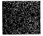
ところで、レーザ光のようなコヒーレント光を拡散面に照射すると、通常の光では見られない斑点状の模様が観察される。このような模様は、スペックル模様と呼ばれている。このスペックル模様は、拡散面の各点で散乱された光が、面上の微視的な凹凸に応じたランダムな位相関係で干渉し合うために生じるものである。 By the way, when a diffusing surface is irradiated with coherent light such as laser light, a spot- like pattern that cannot be seen with normal light is observed. Such a pattern is called a speckle pattern. This speckle pattern is generated because light scattered at each point on the diffusing surface interferes with each other in a random phase relationship according to microscopic unevenness on the surface.
ここで、上記したレーザを光源として用いたプロジェクタでは、スクリーン上において、このようなスペックル模様(干渉パターン)が表示画像に重畳される。このため、人間の眼には強度のランダムノイズとして認識され、表示画質が低下してしまうことになる。 Here, in a projector using the above laser as a light source, such a speckle pattern (interference pattern) is superimposed on a display image on a screen. For this reason, it is recognized by human eyes as intense random noise, and the display image quality deteriorates.
そこで、レーザを光源として用いたプロジェクタにおいて、このようなスペックル模様(スペックルノイズ)の発生を低減する手法として、プロジェクタ内でレーザ光が通過する所定の光学素子やスクリーンを微小振動させるようにしたものが提案されている。一般に、人間の眼および脳は、約20〜50ms内の画像のちらつきは判別できない。つまり、その時間内の画像は眼の中で積分され、平均化されている。したがって、この時間内に、スクリーン上において独立のスペックルパターンを多数重量させることにより、スペックルノイズを人間の眼の中で気にならない程度に平均化しようとするものである。この手法を用いることにより、レーザ光に起因した干渉パターンの発生を低減することが可能となる。 Therefore, in a projector using a laser as a light source, as a technique for reducing the occurrence of such a speckle pattern (speckle noise), a predetermined optical element or a screen through which the laser beam passes in the projector is microvibrated. What has been proposed. In general, the human eye and brain cannot discern flickering of an image within about 20 to 50 ms. That is, the images within that time are integrated and averaged in the eye. Therefore, within this time period, a large number of independent speckle patterns are weighted on the screen so that speckle noise is averaged to such an extent that it does not matter in human eyes. By using this method, it is possible to reduce the generation of interference patterns due to laser light.
しかしながら、何らかの要因で上記した光学素子の振動が停止してしまった場合、上記の原理による干渉パターンの低減作用がなされなくなるため、そのような場合には、結局のところ干渉パターンが発生してしまい、表示画質が劣化してしまうことになる。すなわち、装置(プロジェクタ)の動作状況に応じた干渉パターンの低減が困難であるため、ユーザにおける利便性が低下してしまっていた。 However, when the vibration of the optical element is stopped for some reason, the interference pattern is not reduced by the above principle. In such a case, an interference pattern is eventually generated. The display image quality will deteriorate. That is, since it is difficult to reduce the interference pattern according to the operation status of the apparatus (projector), the convenience for the user has been reduced.
本発明はかかる問題点に鑑みてなされたもので、その目的は、ユーザにおける利便性を向上させることが可能な照明装置および表示装置を提供することにある。 The present invention has been made in view of such problems, and an object thereof is to provide an illumination device and a display device capable of improving convenience for a user.
本発明の照明装置は、レーザ光源を含む光源部と、レーザ光源からのレーザ光が通過する光学素子と、この光学素子を振動させる駆動部と、この駆動部による駆動動作中において光学素子の振動が停止したときに、光源部からの出射光の輝度を低下させる制御と、その振動が停止したことを外部へ警告する制御とのうちの少なくとも一方の制御を行う制御部とを備えたものである。上記駆動部は、光学素子を振動させる際に流れる駆動電流を電圧として検出する抵抗素子を有している。上記制御部は、この抵抗素子による検出電圧の大きさに基づいて、光学素子の振動が停止しているのか否かを判断すると共に、上記検出電圧の値が所定の電圧範囲よりも小さいときには、駆動部内において断線が生じていることにより光学素子の振動が停止していると判断し、上記検出電圧の値が上記電圧範囲よりも大きいときには、駆動部内において異物が介在していることにより光学素子の振動が停止していると判断する。 The illumination device of the present invention includes a light source unit including a laser light source, an optical element through which laser light from the laser light source passes, a drive unit that vibrates the optical element, and vibration of the optical element during a drive operation by the drive unit. A controller that controls at least one of the control to reduce the brightness of the light emitted from the light source unit and the control to warn the outside that the vibration has stopped. is there. The drive unit includes a resistance element that detects a drive current that flows when the optical element is vibrated as a voltage. The control unit determines whether the vibration of the optical element is stopped based on the magnitude of the detection voltage by the resistance element, and when the value of the detection voltage is smaller than a predetermined voltage range, When it is determined that the vibration of the optical element is stopped due to the disconnection in the drive unit, and the value of the detection voltage is larger than the voltage range, a foreign object is present in the drive unit and the optical element It is determined that the vibration has stopped.
本発明の表示装置は、照明光を出射する上記本発明の照明装置と、照明光を映像信号に基づいて変調する光変調素子とを備えたものである。 A display device of the present invention includes the above-described illumination device of the present invention that emits illumination light, and a light modulation element that modulates the illumination light based on a video signal.
本発明の照明装置および表示装置では、レーザ光源からのレーザ光が通過する光学素子が振動することにより、レーザ光に起因した干渉パターンの発生が低減する。また、駆動部による駆動動作中において光学素子の振動が停止したときに、光源部からの出射光の輝度を低下させる制御と、その振動が停止したことを外部へ警告する制御とのうちの少なくとも一方の制御が行われる。これにより、何らかの要因で光学素子の振動が停止してしまった場合であっても、それに起因した干渉パターンの発生を見えにくくしたり、振動が停止したことをユーザへ警告したりすることができる。すなわち、装置の動作状況に応じた干渉パターンの低減を実現し得る。 In the illumination device and the display device of the present invention, the optical element through which the laser light from the laser light source vibrates, thereby reducing the occurrence of interference patterns due to the laser light. In addition, when the vibration of the optical element is stopped during the drive operation by the drive unit, at least one of the control for reducing the luminance of the emitted light from the light source unit and the control for warning the outside that the vibration has stopped One control is performed. Thereby, even when the vibration of the optical element has stopped for some reason, it is possible to make it difficult to see the occurrence of the interference pattern due to the stop or warn the user that the vibration has stopped. . That is, it is possible to reduce the interference pattern according to the operation status of the apparatus.
本発明の照明装置および表示装置によれば、駆動部による駆動動作中において光学素子の振動が停止したときに、光源部からの出射光の輝度を低下させる制御と、その振動が停止したことを外部へ警告する制御とのうちの少なくとも一方の制御を行うようにしたので、装置の動作状況に応じた干渉パターンの低減を実現することができ、ユーザにおける利便性を向上させることが可能となる。 According to the illumination device and the display device of the present invention, when the vibration of the optical element is stopped during the driving operation by the driver, and the control for reducing the luminance of the light emitted from the light source unit, that the vibration is stopped Since at least one of the control for warning to the outside is performed, it is possible to reduce the interference pattern according to the operation status of the apparatus and to improve the convenience for the user. .
以下、本発明の実施の形態について、図面を参照して詳細に説明する。なお、説明は以下の順序で行う。
1.実施の形態(抵抗素子による検出電圧の大きさに応じた制御の例)
2.変形例
Hereinafter, embodiments of the present invention will be described in detail with reference to the drawings. The description will be given in the following order.
1. Embodiment (an example of control according to the magnitude of a detection voltage by a resistance element)
2. Modified example
<実施の形態>
[表示装置1の概略構成]
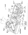
図1は、本発明の一実施の形態に係る表示装置(表示装置1)の概略構成(断面構成)を斜視図で表すものである。表示装置1は、図示しないスクリーン(被投射面)に対して映像(映像光)を投射する投射型の表示装置である。この表示装置1は、筐体10内に、赤色レーザ11R、緑色レーザ11G、青色レーザ11B、コリメータレンズ12R,12G,12B、ダイクロイックプリズム131,132、光学装置14およびフライアイレンズ15を備えている。表示装置1はまた、偏光ビームスプリッタ(PBS;Polarization Beam Splitter)16、反射型液晶素子17、投射レンズ18(投射光学系)および制御部19を備えている。これらのうち、赤色レーザ11R、緑色レーザ11G、青色レーザ11B、コリメータレンズ12R,12G,12B、ダイクロイックプリズム131,132、光学装置14、フライアイレンズ15および制御部19が、本発明の一実施の形態に係る照明装置(照明装置2)を構成している。なお、図中に示したZ1は光軸を表している。
<Embodiment>
[Schematic Configuration of Display Device 1]
FIG. 1 is a perspective view showing a schematic configuration (cross-sectional configuration) of a display device (display device 1) according to an embodiment of the present invention. The display device 1 is a projection type display device that projects an image (image light) onto a screen (projected surface) (not shown). The display device 1 includes a
赤色レーザ11R、緑色レーザ11Gおよび青色レーザ11Bはそれぞれ、赤色レーザ光、緑色レーザ光または青色レーザ光を発する3種類の光源である。これらのレーザ光源により光源部が構成されており、ここでは、これら3種類の光源がいずれもレーザ光源となっている。赤色レーザ11R、緑色レーザ11Gおよび青色レーザ11Bはそれぞれ、例えば半導体レーザや固体レーザ等からなる。
The
コリメータレンズ12R,12G,12Bは、赤色レーザ11Rから出射された赤色レーザ光、緑色レーザ11Gから出射された緑色レーザ光、青色レーザ11Bから出射されたレーザ光をそれぞれ、コリメートして平行光とするためのレンズである。
The
ダイクロイックプリズム131は、コリメータレンズ12Bにより平行光とされた青色レーザ光を選択的に透過させる一方、コリメータレンズ12Rにより平行光とされた赤色レーザ光を選択的に反射させるプリズムである。ダイクロイックプリズム132は、ダイクロイックプリズム131から出射した青色レーザ光および赤色レーザ光を選択的に透過させる一方、コリメータレンズ12Gにより平行光とされた緑色レーザ光を選択的に反射させるプリズムである。これにより、赤色レーザ光、緑色レーザ光および青色レーザ光に対する色合成(光路合成)がなされるようになっている。
The
光学装置14は、上記した光源部(赤色レーザ11R、緑色レーザ11Gおよび青色レーザ11B)と、反射型液晶素子17との間(ここでは、ダイクロイックプリズム132とフライアイレンズ15との間の光路上)に配置されている。この光学装置14は、後述するスペックルノイズ(干渉パターン)を低減するための光学素子(光学素子140)を有するものである。なお、この光学装置14の詳細構成については後述する(図2)。
The
フライアイレンズ15は、基板上に複数のレンズが2次元配置されたものであり、これらのレンズの配列に応じて入射光束を空間的に分割して出射させるものである。これにより、このフライアイレンズ15からの出射光が均一化され(面内の強度分布が均一化され)、照明装置2からの照明光として出射されるようになっている。
The fly-
偏光ビームスプリッタ16は、特定の偏光(例えばp偏光)を選択的に透過させると共に、他方の偏光(例えばs偏光)を選択的に反射させる光学部材である。これにより、フライアイレンズ15から出射した照明光(例えばs偏光)が選択的に反射されて反射型液晶素子17へ入射すると共に、この反射型液晶素子17から出射した映像光(例えばp偏光)が選択的に透過し、投射レンズ18へ入射するようになっている。
The
反射型液晶素子17は、光源部(赤色レーザ11R、緑色レーザ11Gおよび青色レーザ11B)からの光(照明装置2からの照明光)を、図示しない表示制御部から供給される映像信号に基づいて変調しつつ反射させることにより、映像光を出射する光変調素子である。このとき、反射型液晶素子17では、入射時と出射時とにおける各偏光(例えば、s偏光またはp偏光)が異なるものとなるように、反射がなされる。このような反射型液晶素子17は、例えばLCOS(Liquid Crystal On Silicon)等の液晶素子からなる。
The reflective
投射レンズ18は、反射型液晶素子17により変調された光(映像光)を、図示しないスクリーンに対して投射(拡大投射)するためのレンズである。これにより、投射光Loutがスクリーン上へ投射されるようになっている。
The
制御部19は、光学装置14内の後述する光学素子140(干渉パターンの発生を低減するための光学素子)に対する駆動部による駆動動作中において、この光学素子140の振動が停止したときに、後述する所定の対処制御を行うものである。具体的には、後述する所定の電圧(検出電圧V1)の大きさに応じて、そのような対処制御を行うようになっている。このような制御部19は、例えばマイクロコンピュータなどにより構成されている。なお、制御部19の詳細については後述する。
When the vibration of the
[光学装置14の詳細構成]
次に、図2を参照して、上記した光学装置14の詳細構成について説明する。図2は、光学装置14の詳細構成例を斜視図で表わしたものである。この光学装置14は、光学素子140、固定部ホルダ141、コイル142、磁石143、ヨーク144、可動部ホルダ145および板バネ146(保持部材)を有している。これらのうち、コイル142および固定部ホルダ141が「固定部」を構成し、光学素子140、磁石143、ヨーク144および板バネ146が、「可動部」を構成している。
[Detailed Configuration of Optical Device 14]
Next, the detailed configuration of the
光学素子140は、前述したようにスペックルノイズを低減するための素子であり、図中に示した光軸Z1上を進行するレーザ光がこの光学素子140を通過するようになっている。この光学素子140は、例えばプリズムアレイ、回折素子またはレンズからなり、ここでは矩形状となっている。
The
固定部ホルダ141は、上記した固定部であるコイル142を保持するためのホルダであり、例えばポリカーボネートや液晶ポリマー等の材料からなる。
The
コイル142は、例えば巻き線コイルからなる。磁石143は、例えばネオジム(Nd)や鉄(Fe)、ホウ素(ボロン;B)等の材料からなる永久磁石である。これらコイル142および磁石143は、電磁力を用いて、光学素子140をレーザ光の光路(図中の光軸Z1に対応)と直交する面内の所定方向(1方向,2方向,回転方向など)、またはこの光路(光軸Z1)に沿って振動(微小振動)させるようになっている。具体的には、ここでは光学素子140を、光軸Z1と直交する面内における所定の1方向(図中の振動方向P1;Y軸方向)に沿って振動させるようになっている。なお、この微小振動の振動量(振幅量)は、例えば±0.5mm程度である。
The
ヨーク144は、磁石143から出力される磁束の方向を制御するための部材であり、例えば鉄(Fe)等の透磁率が高い材料からなる。また、このヨーク144は、ここでは磁石143からの磁束が装置外部(光学装置14の外部)へ出力されないように、磁石143の周囲に配置されている。具体的には、矩形状の磁石143における、コイル142側の面の対向面(光学素子140側の面)(Y−Z面)およびこれらの面の側面(Z−X面)をそれぞれ取り囲むように、ヨーク144が配置されている。
The yoke 144 is a member for controlling the direction of the magnetic flux output from the
可動部ホルダ145は、上記した可動部としての光学素子140、磁石143、ヨーク144および板バネ146を保持するためのホルダであり、ここでは、光学素子140とヨーク144との間に配置されている。可動部ホルダ145は、例えばポリカーボネートや液晶ポリマー等の材料からなる。
The
板バネ146は光学素子140を保持する保持部材であり、ここでは、矩形状の光学素子140における対向する一対の側面(Z−X面)側にそれぞれ配置されている。この板バネ146は弾性部材であり、例えばSUS301−CSP等のバネ材料からなる。また、板バネ146では、光反射率を低減するための表面処理(例えば、黒色塗装、艶消し処理、またはブラスト処理(サンドブラスト等)など)が施されているようにするのが望ましい。具体的には、板バネ146の表面は黒色となっているのが望ましく、例えば、400〜700nmの波長帯域の光に対する反射率が10%以下となるような表面処理が施されていることが望ましい。これにより、板バネ146が金属製である場合に、この表面での乱反射光に起因した表示画質の低下を低減することができるからである。
The
[光学素子140に対する駆動部の要部構成]
次に、図3を参照して、上記した光学素子140に対する駆動部の要部構成について説明する。図3は、光学素子140に対する駆動部の要部構成例を、前述した制御部19とともに回路図で表わしたものである。この光学素子140に対する駆動部は、上記したコイル142および磁石143等に加え、例えば図3に示した信号発生器147および抵抗素子148を有している。ここで、信号発生器147の一端はコイル142の一端に接続され、他端は接地されている(グランドに接続されている)。コイル142の他端は抵抗素子148の一端に接続され、抵抗素子148の他端は接地されている。
[Configuration of main part of drive unit for optical element 140]
Next, with reference to FIG. 3, the structure of the main part of the drive unit for the
信号発生器147は、光学素子140を駆動する(振動させる)際に用いる交流電圧を発生する電源である。これにより、図3中に示した交流の駆動電流I1がコイル142を流れ、その結果、駆動する際の電磁力が発生するようになっている。
The
抵抗素子148は、コイル142を流れる上記駆動電流I1を電圧として検出する素子である。具体的には、駆動電流I1の大きさに応じて抵抗素子148の両端間に発生する電位(電圧)が、検出電圧V1(=抵抗素子148の抵抗値×駆動電流I1)として検出される。なお、このようにして検出された検出電圧V1(のデータ)は、図3に示したように、制御部19へ入力されるようになっている。
The
[表示装置1の作用・効果]
(1.表示動作)
この表示装置1では、まず、照明装置2から以下のようにして照明光が出射される。すなわち、赤色レーザ11R、緑色レーザ11Gおよび青色レーザ11Bからそれぞれ出射された光(レーザ光)が、コリメータレンズ12R,12G,12Bによってそれぞれコリメートされ、平行光となる。次いで、このようにして平行光とされた各レーザ光(赤色レーザ光、緑色レーザ光および青色レーザ光)は、ダイクロイックプリズム131,132によって色合成(光路合成)がなされる。光路合成がなされた各レーザ光は、光学装置14を通過したのち、フライアイレンズ15へ入射する。この入射光はフライアイレンズ15によって均一化(面内の強度分布の均一化)がなされ、照明光として出射される。
[Operation and Effect of Display Device 1]
(1. Display operation)
In the display device 1, first, illumination light is emitted from the
次いで、このフライアイレンズ15からの出射光(照明装置2からの照明光)は、偏光ビームスプリッタ16によって選択的に反射され、反射型液晶素子17へ入射する。反射型液晶素子17では、この入射光が映像信号に基づいて変調されつつ反射されることにより、映像光として出射する。ここで、この反射型液晶素子17では、入射時と出射時とにおける各偏光が異なるものとなるため、反射型液晶素子17から出射した映像光は選択的に偏光ビームスプリッタ16を透過し、投射レンズ18へと入射する。そして、この入射光(映像光)は、投射レンズ18によって、図示しないスクリーンに対して投射(拡大投射)される。
Next, the light emitted from the fly-eye lens 15 (illumination light from the illumination device 2) is selectively reflected by the
この際、赤色レーザ11R、緑色レーザ11Gおよび青色レーザ11Bはそれぞれ、時分割的に順次発光(パルス発光)し、各レーザ光(赤色レーザ光,緑色レーザ光,青色レーザ光)を出射する。そして、反射型液晶素子17では、各色成分(赤色成分、緑色成分、青色成分)の映像信号に基づいて、対応する色のレーザ光が時分割的に順次変調される。これにより、映像信号に基づくカラー映像表示が表示装置1においてなされる。
At this time, each of the
(2.干渉パターンの低減動作)
次に、本発明の特徴的部分の1つである、後述する干渉パターンの低減動作について、比較例と比較しつつ詳細に説明する。
(2. Interference pattern reduction operation)
Next, an interference pattern reduction operation described later, which is one of the characteristic parts of the present invention, will be described in detail in comparison with a comparative example.
(2−1.比較例)
図4は、比較例に係る表示装置(表示装置100)の全体構成を表したものである。この比較例の表示装置100は、本実施の形態の表示装置1と同様に、スクリーン(ここではスクリーン107)に対して映像光を投射する投射型の表示装置である。表示装置100は、赤色レーザ101R、緑色レーザ101G、青色レーザ101B、光強度変調器102R,102G,102B、ダイクロイックミラー103R,103G,103B、ポリゴンミラー104、ガルバノミラー105およびf−θレンズ106を備えている。
(2-1. Comparative example)
FIG. 4 illustrates the overall configuration of a display device (display device 100) according to a comparative example. The
この表示装置100では、赤色レーザ101Rから出射されたレーザ光は、光強度変調器102Rにおいて映像信号に基づいて変調されつつ透過し、映像光として出射する。同様に、緑色レーザ101Gから出射されたレーザ光は、光強度変調器102Gにおいて映像信号に基づいて変調されつつ透過し、映像光として出射する。また、青色レーザ101Bから出射されたレーザ光は、光強度変調器102Bにおいて映像信号に基づいて変調されつつ透過し、映像光として出射する。このようにして光強度変調器102R,102G,102Bからそれぞれ出射された各色の映像光は、ダイクロイックミラー103R,103G,103Bにおいて色合成(光路合成)がなされ、カラー映像に対応する映像光としてポリゴンミラー104へ入射する。この入射光は、水平同期信号に同期して高速回転(図中の矢印P101参照)するポリゴンミラー104によって、水平方向に偏向される。また、このようにして水平方向に偏向された光は、更に、垂直同期信号に同期して反射角を変化させる(図中の矢印P102参照)ガルバノミラー105によって、垂直方向に偏向される。そして、このようにして2次元に偏向されたレーザ光は、f−θレンズ106によってスクリーン107に対して投射(拡大投射)され、これにより映像信号に基づくカラー映像表示が表示装置100においてなされる。
In the
ところで、レーザ光のようなコヒーレント光を拡散面に照射すると、例えば図5に示した写真のように、通常の光では見られない斑点状の模様が観察される。このような模様は、スペックル模様と呼ばれている。このスペックル模様は、拡散面の各点で散乱された光が、面上の微視的な凹凸に応じたランダムな位相関係で干渉し合うために生じるものである。なお、このようなスペックル模様は、一般には2種類に大別される。1つ目は、結像系を通さないで観察されるものであり、回折界スペックルと呼ばれている。この回折界スペックルは、例えばCCD(Charge Coupled Device)カメラに対してレンズを付けずに拡散光をみたときに観察される。回折界スペックルでは、拡散面上の光の当たっている全ての点が干渉に寄与することになる。2つ目は、結像系を介して観察したときにみられるものであり、眼で拡散面をみたときに見えるスペックルがこれに相当する。このようなスペックルは、像界スペックルと呼ばれている。 By the way, when a diffusing surface is irradiated with coherent light such as laser light, a spot- like pattern that cannot be seen with normal light is observed, for example, as shown in the photograph of FIG. Such a pattern is called a speckle pattern. This speckle pattern is generated because light scattered at each point on the diffusing surface interferes with each other in a random phase relationship according to microscopic unevenness on the surface. Such speckle patterns are generally roughly divided into two types. The first one is observed without passing through the imaging system, and is called diffraction field speckle. This diffraction field speckle is observed, for example, when the diffused light is viewed without attaching a lens to a CCD (Charge Coupled Device) camera. In diffracted field speckles, all points on the diffusing surface that are exposed to light contribute to interference. The second one is observed when observed through an imaging system, and corresponds to speckles that can be seen when viewing the diffusing surface with the eyes. Such speckle is called image field speckle.
ここで、上記比較例の表示装置100のようにレーザ光源を用いたプロジェクタでは、スクリーン上において、このようなスペックル模様(干渉パターン)が表示画像に重畳される。このため、人間の眼には強度のランダムノイズとして認識され、表示画質が低下してしまうことになる。
Here, in a projector using a laser light source like the
そこで、レーザ光源を用いたプロジェクタにおいて、このようなスペックル模様(スペックルノイズ)の発生を低減するため、プロジェクタ内でレーザ光が通過する所定の光学素子やスクリーンを、微小振動させる手法が考えられる。一般に、人間の眼および脳は、約20〜50ms内の画像のちらつきは判別できない。つまり、その時間内の画像は眼の中で積分され、平均化されている。したがって、この時間内に、スクリーン上において独立のスペックルパターンを多数重量させることにより、スペックルノイズを人間の眼の中で気にならない程度に平均化しようとするものである。 Therefore, in order to reduce the occurrence of such speckle patterns (speckle noise) in a projector using a laser light source, a method of minutely vibrating a predetermined optical element or screen through which laser light passes in the projector is considered. It is done. In general, the human eye and brain cannot discern flickering of an image within about 20 to 50 ms. That is, the images within that time are integrated and averaged in the eye. Therefore, within this time period, a large number of independent speckle patterns are weighted on the screen so that speckle noise is averaged to such an extent that it does not matter in human eyes.
(2−2.本実施の形態)
そこで、本実施の形態の光学装置14においても、図1および図2に示したように、レーザ光が通過する光学素子140が、このレーザ光の光路(光軸Z1)と直交する面内(XY面内;ここではY軸方向に沿った振動方向P1)で振動(微小振動)する。具体的には、コイル142および磁石143を含む駆動部によって、電磁力を用いてそのような振動がなされるように、光学素子140が駆動される。これにより、上記した原理によって、レーザ光に起因したスペックルノイズ(干渉パターン)の発生が低減する。
(2-2. The present embodiment)
Therefore, also in the
ところが、何らかの要因で光学素子140の振動が停止してしまった場合、上記の原理による干渉パターンの低減作用がなされなくなるため、そのような場合には、結局のところ干渉パターンが発生してしまい、表示画質が劣化してしまうことになる。すなわち、表示装置1の動作状況に応じた干渉パターンの低減が困難であるため、ユーザにおける利便性が低下してしまうことになる。
However, when the vibration of the
ここで、光学素子140が振動停止する要因(原因)としては、主に以下の2つの要因が挙げられる。
・要因1:駆動部内(例えば、図3に示した駆動電流I1の電流経路)において断線が生じ、駆動電流I1が流れなくなっているため
・要因2:駆動部内(例えば、図2中におけるコイル142と磁石143との隙間)において異物(例えば磁性粉など)が介在している(挟まっている,巻き込まれている)ことにより、機械的に振動が阻害されているため
Here, as the factor (cause) that causes the
Factor 1: Because a disconnection occurs in the driving unit (for example, the current path of the driving current I1 shown in FIG. 3), and the driving current I1 does not flow. Factor 2: In the driving unit (for example, the
(検出電圧V1の大きさと光学素子140の振動停止の有無との関係)
そこで本実施の形態では、制御部19において、図3に示した抵抗素子148の両端間の電圧(検出電圧V1)の値を利用して、上記した2つの要因による光学素子140の振動停止の有無(光学素子140が正常に動作しているのか否か)を判断している。
(Relationship between magnitude of detection voltage V1 and presence / absence of vibration stop of optical element 140)
Therefore, in the present embodiment, the
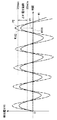
ここで図6を参照して、検出電圧V1の波形と光学素子140の振動停止の有無との関係について説明する。図6は、この検出電圧V1の波形の時間変化の一例を表したものである。
Here, with reference to FIG. 6, the relationship between the waveform of the detection voltage V1 and the presence or absence of vibration stop of the
まず、光学素子140が正常に動作しているとき(光学素子140が振動しているとき)には、コイル142に駆動電流I1が流れ、所定の電圧範囲ΔV内の検出電圧V1が生じる(図6中の電圧波形W1参照)。この電圧範囲ΔVとは、例えば表示装置1における動作保証電圧範囲であり、最小閾値電圧Vthmin以上かつ最大閾値電圧Vthmax以下の電圧範囲となっている。
First, when the
これに対して、上記した要因1によって光学素子140が正常に動作していないとき(光学素子140の振動が停止しているとき)には、上記した断線に起因して、信号発生器147が交流電圧を発生させても、コイル142に駆動電流I1が流れないことになる。したがって、駆動電流I1の値が小さくなる(流れない)ことから、検出電圧V1の値は電圧範囲ΔV(最小閾値電圧Vthmin)よりも小さく(低く)なり、例えば常に0Vとなる(図6中の電圧波形W101参照)。
On the other hand, when the
一方、上記した要因2によって光学素子140の振動が停止しているときには、上記した異物の介在による機械的な振動阻害に起因して、コイル142において逆起電力が発生しなくなるため、逆に駆動電流I1の値が大きくなる。したがって、駆動電流I1の値が大きくなることから、検出電圧V1の値も、逆に電圧範囲ΔV(最大閾値電圧Vthmax)よりも大きく(高く)なる(図6中の電圧波形W102参照)。ここで、この要因2によって光学素子140の振動が停止しているときに駆動電流I1の値が大きくなるのは、以下の理由によるものである。
On the other hand, when the vibration of the
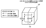
すなわち、まず、例えば図7に示したように、コイル142に電流(駆動電流I1)が流れ、その電流の流れる方向と直交する方向に磁束が発生しているときには、これらの方向のいずれとも直交する方向に沿って、コイル142に力が働く(フレミング左手の法則)。このような力がコイル142に働くことを利用して、駆動部によって光学素子140を振動させている。
That is, first, as shown in FIG. 7, for example, when a current (drive current I1) flows through the
このとき、それと同時に、例えば図8に示したように、このようなコイル142の動作(変位)によって、図7に示した方向と逆向きの電流がコイル142に流れることになる(フレミング右手の法則)。すなわち、このときに発生する逆起電力に起因して、コイル142に流れる電流(駆動電流I1)は、全体として小さくなっている。ところが、上記した要因2によって光学素子140の振動が停止している(異物の介在によって機械的な振動が阻害されている)ときには、振動の停止によって逆起電力が発生しないため、コイル142に流れる駆動電流I1が逆に大きくなるのである。
At the same time, for example, as shown in FIG. 8, a current in the direction opposite to the direction shown in FIG. law). That is, due to the counter electromotive force generated at this time, the current flowing through the coil 142 (drive current I1) is reduced as a whole. However, when the vibration of the
以上のような検出電圧V1の大きさと光学素子140の振動停止の有無との関係(更には要因1,2のいずれによる振動停止であるのか)を利用して、本実施の形態では、制御部19において以下説明するような所定の制御動作を行う。具体的には、制御部19は、前述した駆動部による駆動動作中において光学素子140の振動が停止したときに(振動が停止したと判断したときに)、後述する所定の対処制御を行う。詳細には、検出電圧V1の大きさに基づいて光学素子140の振動が停止しているのか否かを判断し、そのような対処制御を行う。より詳細には、制御部19は、検出電圧V1の値が、上記した電圧範囲ΔV(最小閾値電圧Vthmin)よりも小さいとき、またはこの電圧範囲ΔV(最大閾値電圧Vthmax)よりも大きいときに、光学素子140の振動が停止していると判断する。
In the present embodiment, the control unit uses the relationship between the magnitude of the detection voltage V1 and the presence or absence of vibration stop of the
(制御部19による制御動作の詳細)
図9は、制御部19による制御動作の一例を流れ図で表わしたものである。この制御動作の際には、制御部19はまず、例えば図3に示したように、駆動部から検出電圧V1のデータを取得する(ステップS11)。次いで、制御部19は、この検出電圧V1が電圧範囲ΔV内の値であるのか否か、つまり、最小閾値電圧Vthmin以上かつ最大閾値電圧Vthmax以下の値である(Vthmin≦V1≦Vthmax)のか否かを判定する(ステップS12)。
(Details of control operation by control unit 19)
FIG. 9 shows an example of a control operation by the
ここで、検出電圧V1が電圧範囲ΔV内の値である(Vthmin≦V1≦Vthmaxを満たす)と判定されたときには(ステップS12:Y)、制御部19は、光学素子140の振動が停止していない(正常に動作している)と判断し、再び最初のステップS11へと戻る。一方、検出電圧V1が電圧範囲ΔV内の値ではない(Vthmin≦V1≦Vthmaxを満たさない)と判定されたときには(ステップS12:N)、制御部19は、何らかの要因によって光学素子140の振動が停止している(正常に動作していない)と判断し、以下の対処制御を行う(ステップS13)。また、この際に制御部19は、検出電圧V1の値が電圧範囲ΔVよりも小さいとき(V1<Vthmim)には、上記した要因1(駆動部内において断線が生じている)ことにより光学素子140の振動が停止していると判断する。一方、検出電圧V1の値が電圧範囲ΔVよりも大きいとき(Vthmax<V1)には、上記した要因2(駆動部内において異物が介在している)ことにより光学素子140の振動が停止していると判断する。
Here, when it is determined that the detection voltage V1 is a value within the voltage range ΔV (Vthmin ≦ V1 ≦ Vthmax is satisfied) (step S12: Y), the
この所定の対処制御としては、例えば以下のものが挙げられる。すなわち、光源部(赤色レーザ11R,緑色レーザ11G,青色レーザ11B)からの出射光(ここではレーザ光)の輝度を低下させる制御と、光学素子140の振動が停止した旨を外部(ユーザ)へ出力(警告)する制御と、のうちの少なくとも一方の制御である。また、このときの出射光の輝度を低下させる制御としては、一例として、レーザ光源(赤色レーザ11R,緑色レーザ11G,青色レーザ11B)からのレーザ光(赤色レーザ光,緑色レーザ光,青色レーザ光)の出射を停止させる制御、または出射されるレーザ光の光量を抑える制御が挙げられる。すなわち、これらのレーザ光源の発光動作を停止させるか、あるいはこの発光動作を抑制させる、という制御である。また、振動が停止した旨を外部へ出力する制御としては、例えば、所定の(警告)ランプを点灯させたり、所定の音(警告音)を発生させたり、モニタ用画面やスクリーン上において所定の表示(警告表示)を行ったりすることが挙げられる。なお、その他にも、モニタ用画面やスクリーン上に所定の選択用画面を表示し、干渉パターンが発生している状態の表示を継続するのか、あるいは上記した出射光の輝度を低下させる制御を行うのか、といった選択肢をユーザへ提供する(ユーザに選択させる)ようにしてもよい。このような対処制御がなされることにより、何らかの要因(例えば上記した要因1,2)で光学素子140の振動が停止してしまった場合であっても、それに起因した干渉パターンの発生を見えにくくしたり、振動が停止した旨をユーザへ警告したりすることができる。すなわち、表示装置1の動作状況に応じた干渉パターンの低減を実現し得る。以上により、図9に示した制御部19による制御動作が終了となる。
Examples of the predetermined countermeasure control include the following. That is, control for lowering the luminance of the light emitted from the light source unit (
以上のように本実施の形態では、駆動部による駆動動作中において光学素子140の振動が停止したときに、制御部19において、赤色レーザ11R,緑色レーザ11G,青色レーザ11Bからの出射光の輝度を低下させる制御と、光学素子140の振動が停止した旨を外部へ出力する制御とのうちの少なくとも一方の制御を行うようにしたので、表示装置1の動作状況に応じた干渉パターンの低減を実現することができ、例えば多少画面が暗くなりつつも画質劣化を抑えることができると共に、ユーザにおける利便性を向上させることが可能となる。
As described above, in the present embodiment, when the vibration of the
また、検出電圧V1の大きさに基づいて光学素子140の振動が停止しているのか否かを判断し、そのような対処制御を行うようにしたので、光学素子140の振動停止の有無に加え、振動停止の要因(上記した要因1,2のいずれによる振動停止であるのか)についても検出(特定)することができる。よって、そのような振動停止(故障)を修理する際に有用な情報(振動停止の要因)についても把握することができ、ユーザにおける利便性を更に向上させることが可能となる。
In addition, since it is determined whether or not the vibration of the
<変形例>
以上、実施の形態を挙げて本発明を説明したが、本発明はこの実施の形態に限定されず、種々の変形が可能である。
<Modification>
While the present invention has been described with reference to the embodiment, the present invention is not limited to this embodiment, and various modifications can be made.
例えば、上記実施の形態では、制御部19が筺体10内に収容されている場合を例に挙げて説明したが、そのような場合には限られず、制御部19が筺体10の外部に配置されているようにしてもよい。
For example, in the above-described embodiment, the case where the
また、上記実施の形態では、光学素子を、レーザ光の光路と直交する面内の所定方向、またはこの光路に沿った方向に振動させる場合について説明したが、この場合には限られない。すなわち、光学素子を振動(微小振動)させるのであれば、他の方向に沿って光学素子を振動させるようにしてもよい。 In the above-described embodiment, the case has been described in which the optical element is vibrated in a predetermined direction in a plane orthogonal to the optical path of the laser light, or in a direction along the optical path. However, the present invention is not limited to this case. That is, if the optical element is vibrated (microvibration), the optical element may be vibrated along another direction.
更に、上記実施の形態では、複数種類(赤色用,緑色用,青色用)の光源がいずれもレーザ光源である場合について説明したが、この場合には限られず、複数種類の光源のうちの少なくとも1つがレーザ光源であればよい。すなわち、光源部内に、レーザ光源と他の光源(例えばLED等)とを組み合わせて設けるようにしてもよい。 Furthermore, in the above-described embodiment, a case has been described in which a plurality of types (red, green, and blue) of light sources are all laser light sources. However, the present invention is not limited to this case, and at least of the plurality of types of light sources. One may be a laser light source. That is, a combination of a laser light source and another light source (such as an LED) may be provided in the light source unit.
加えて、上記実施の形態では、光変調素子が反射型の液晶素子である場合を例に挙げて説明したが、この場合には限られず、例えば透過型の液晶素子であってもよく、更には、液晶素子以外の光変調素子であってもよい。 In addition, in the above-described embodiment, the case where the light modulation element is a reflective liquid crystal element has been described as an example. However, the present invention is not limited to this, and may be, for example, a transmissive liquid crystal element. May be a light modulation element other than a liquid crystal element.
また、上記実施の形態では、異なる波長の光を発する3種類の光源を用いた場合について説明したが、例えば3種類の光源ではなく、1種類や2種類,4種類以上の光源を用いるようにしてもよい。 In the above embodiment, the case where three types of light sources that emit light of different wavelengths are used has been described. For example, instead of three types of light sources, one type, two types, or four or more types of light sources are used. May be.
更に、上記実施の形態では、光学装置、照明装置および表示装置の各構成要素(光学系)を具体的に挙げて説明したが、全ての構成要素を備える必要はなく、また、他の構成要素を更に備えていてもよい。 Furthermore, in the above-described embodiment, each component (optical system) of the optical device, the illumination device, and the display device has been specifically described. However, it is not necessary to include all the components, and other components May be further provided.
加えて、上記実施の形態では、光変調素子により変調された光をスクリーンに投射する投射光学系(投影レンズ)を備え、投射型の表示装置として構成されている場合について説明したが、本発明は、直視型の表示装置などにも適用することが可能である。 In addition, in the above-described embodiment, the case where the projection optical system (projection lens) that projects the light modulated by the light modulation element on the screen is provided and configured as a projection display device has been described. Can be applied to a direct-view display device or the like.
1…表示装置、10…筐体、11R…赤色レーザ、11G…緑色レーザ、11B…青色レーザ、12R,12G,12B…コリメータレンズ、131,132…ダイクロイックプリズム、14…光学装置、140…光学素子、141…固定部ホルダ、142…コイル、143…磁石、144…ヨーク、145…可動部ホルダ、146…板バネ、147…信号発生器、148…抵抗素子、15…フライアイレンズ、16…偏光ビームスプリッタ、17…反射型液晶素子、18…投射レンズ、19…制御部、2…照明装置、Z1…光軸、P1…振動方向、Lout…投射光、I1…駆動電流、V1…検出電圧、Vthmin…最小閾値電圧、Vthmax…最大閾値電圧、ΔV…電圧範囲、W1…電圧波形。 DESCRIPTION OF SYMBOLS 1 ... Display apparatus, 10 ... Housing | casing, 11R ... Red laser, 11G ... Green laser, 11B ... Blue laser, 12R, 12G, 12B ... Collimator lens, 131, 132 ... Dichroic prism, 14 ... Optical apparatus, 140 ... Optical element , 141, fixed part holder, 142, coil, 143, magnet, 144, yoke, 145, movable part holder, 146, leaf spring, 147, signal generator, 148, resistance element, 15, fly eye lens, 16, polarized light Beam splitter, 17 ... reflective liquid crystal element, 18 ... projection lens, 19 ... control unit, 2 ... lighting device, Z1 ... optical axis, P1 ... vibration direction, Lout ... projection light, I1 ... drive current, V1 ... detection voltage, Vthmin: minimum threshold voltage, Vthmax: maximum threshold voltage, ΔV: voltage range, W1: voltage waveform.
Claims (8)
前記レーザ光源からのレーザ光が通過する光学素子と、
前記光学素子を振動させる駆動部と、
前記駆動部による駆動動作中において前記光学素子の振動が停止したときに、前記光源部からの出射光の輝度を低下させる制御と、その振動が停止したことを外部へ警告する制御と、のうちの少なくとも一方の制御を行う制御部と
を備え、
前記駆動部は、前記光学素子を振動させる際に流れる駆動電流を電圧として検出する抵抗素子を有し、
前記制御部は、
前記抵抗素子による検出電圧の大きさに基づいて、前記光学素子の振動が停止しているのか否かを判断すると共に、
前記検出電圧の値が所定の電圧範囲よりも小さいときには、前記駆動部内において断線が生じていることにより前記光学素子の振動が停止していると判断し、
前記検出電圧の値が前記電圧範囲よりも大きいときには、前記駆動部内において異物が介在していることにより前記光学素子の振動が停止していると判断する
照明装置。 A light source unit including a laser light source;
An optical element through which laser light from the laser light source passes,
A drive unit for vibrating the optical element;
A control for lowering the luminance of the light emitted from the light source unit when the vibration of the optical element stops during the driving operation by the driving unit, and a control for warning the outside that the vibration has stopped. and a control unit for performing at least one of the control,
The drive unit includes a resistance element that detects a drive current that flows when the optical element is vibrated as a voltage;
The controller is
Based on the magnitude of the voltage detected by the resistance element, it is determined whether or not the vibration of the optical element is stopped,
When the value of the detection voltage is smaller than a predetermined voltage range, it is determined that the vibration of the optical element is stopped due to disconnection in the drive unit,
An illumination device that determines that the vibration of the optical element is stopped due to the presence of foreign matter in the drive unit when the value of the detection voltage is larger than the voltage range .
請求項1に記載の照明装置。 The illuminating device according to claim 1 , wherein the control unit performs control for stopping emission of laser light from the laser light source as control for reducing luminance of the emitted light.
請求項1または請求項2に記載の照明装置。 The illumination device according to claim 1, wherein the optical element is a prism array, a diffraction element, or a lens.
請求項1ないし請求項3のいずれか1項に記載の照明装置。 The lighting device according to any one of claims 1 to 3 , wherein the light source unit includes three types of light sources that emit red light, green light, and blue light.
請求項4に記載の照明装置。 The lighting device according to claim 4 , wherein at least one of the three types of light sources is the laser light source.
前記照明光を映像信号に基づいて変調する光変調素子と
を備え、
前記照明装置は、
レーザ光源を含む光源部と、
前記レーザ光源からのレーザ光が通過する光学素子と、
前記光学素子を振動させる駆動部と、
前記駆動部による駆動動作中において前記光学素子の振動が停止したときに、前記光源部からの出射光の輝度を低下させる制御と、その振動が停止したことを外部へ警告する制御と、のうちの少なくとも一方の制御を行う制御部と
を有し、
前記駆動部は、前記光学素子を振動させる際に流れる駆動電流を電圧として検出する抵抗素子を有し、
前記制御部は、
前記抵抗素子による検出電圧の大きさに基づいて、前記光学素子の振動が停止しているのか否かを判断すると共に、
前記検出電圧の値が所定の電圧範囲よりも小さいときには、前記駆動部内において断線が生じていることにより前記光学素子の振動が停止していると判断し、
前記検出電圧の値が前記電圧範囲よりも大きいときには、前記駆動部内において異物が介在していることにより前記光学素子の振動が停止していると判断する
表示装置。 An illumination device that emits illumination light;
A light modulation element that modulates the illumination light based on a video signal,
The lighting device includes:
A light source unit including a laser light source;
An optical element through which laser light from the laser light source passes,
A drive unit for vibrating the optical element;
A control for lowering the luminance of the light emitted from the light source unit when the vibration of the optical element stops during the driving operation by the driving unit, and a control for warning the outside that the vibration has stopped. have a control unit for performing at least one of the control,
The drive unit includes a resistance element that detects a drive current that flows when the optical element is vibrated as a voltage;
The controller is
Based on the magnitude of the voltage detected by the resistance element, it is determined whether or not the vibration of the optical element is stopped,
When the value of the detection voltage is smaller than a predetermined voltage range, it is determined that the vibration of the optical element is stopped due to disconnection in the drive unit,
A display device that, when the value of the detection voltage is larger than the voltage range, determines that the vibration of the optical element is stopped due to the presence of foreign matter in the drive unit .
請求項6に記載の表示装置。 The display device according to claim 6 , further comprising a projection optical system that projects the illumination light modulated by the light modulation element onto a projection surface.
請求項6または請求項7に記載の表示装置。 The display device according to claim 6 or claim 7 wherein the light modulator is a liquid crystal element.
Priority Applications (3)
| Application Number | Priority Date | Filing Date | Title |
|---|---|---|---|
| JP2011053988A JP5790040B2 (en) | 2011-03-11 | 2011-03-11 | Illumination device and display device |
| US13/367,919 US8917223B2 (en) | 2011-03-11 | 2012-02-07 | Illumination unit and display apparatus |
| CN201210054249.1A CN102681199B (en) | 2011-03-11 | 2012-03-02 | Lighting unit and display device |
Applications Claiming Priority (1)
| Application Number | Priority Date | Filing Date | Title |
|---|---|---|---|
| JP2011053988A JP5790040B2 (en) | 2011-03-11 | 2011-03-11 | Illumination device and display device |
Publications (3)
| Publication Number | Publication Date |
|---|---|
| JP2012189858A JP2012189858A (en) | 2012-10-04 |
| JP2012189858A5 JP2012189858A5 (en) | 2014-04-03 |
| JP5790040B2 true JP5790040B2 (en) | 2015-10-07 |
Family
ID=46795144
Family Applications (1)
| Application Number | Title | Priority Date | Filing Date |
|---|---|---|---|
| JP2011053988A Active JP5790040B2 (en) | 2011-03-11 | 2011-03-11 | Illumination device and display device |
Country Status (3)
| Country | Link |
|---|---|
| US (1) | US8917223B2 (en) |
| JP (1) | JP5790040B2 (en) |
| CN (1) | CN102681199B (en) |
Cited By (1)
| Publication number | Priority date | Publication date | Assignee | Title |
|---|---|---|---|---|
| US11605325B2 (en) | 2019-10-07 | 2023-03-14 | Samsung Electronics Co., Ltd. | Display device and method of operating the same |
Families Citing this family (4)
| Publication number | Priority date | Publication date | Assignee | Title |
|---|---|---|---|---|
| JP2014186206A (en) * | 2013-03-25 | 2014-10-02 | Hitachi Media Electoronics Co Ltd | Light irradiation device |
| JP6394693B2 (en) | 2014-03-18 | 2018-10-03 | 株式会社リコー | Light source device and image projection apparatus having the light source device |
| JP6693043B2 (en) * | 2014-12-26 | 2020-05-13 | 日亜化学工業株式会社 | Light source device and projector |
| DE102021202733A1 (en) * | 2021-03-22 | 2022-09-22 | Robert Bosch Gesellschaft mit beschränkter Haftung | Optical beam combiner |
Family Cites Families (19)
| Publication number | Priority date | Publication date | Assignee | Title |
|---|---|---|---|---|
| JPH02216350A (en) * | 1989-02-15 | 1990-08-29 | Aisin Seiki Co Ltd | Waterdrop remover device |
| JP2538088B2 (en) * | 1990-01-23 | 1996-09-25 | 松下電器産業株式会社 | Driving method for ultrasonic motor |
| IL138374A (en) * | 1998-03-11 | 2004-07-25 | Nikon Corp | Ultraviolet laser apparatus and exposure apparatus comprising the ultraviolet laser apparatus |
| JP4083941B2 (en) * | 1999-09-03 | 2008-04-30 | 株式会社リコー | Coordinate input device |
| JP3721337B2 (en) * | 2002-03-22 | 2005-11-30 | ファナック株式会社 | Laser oscillator |
| JP4573573B2 (en) * | 2003-05-28 | 2010-11-04 | 富士フイルム株式会社 | Projection-type image display device |
| KR100595519B1 (en) | 2004-03-03 | 2006-07-03 | 엘지전자 주식회사 | Electromagnetic actuator for reducing the degeneration of image quality in display systems |
| US7660037B2 (en) * | 2006-06-06 | 2010-02-09 | Seiko Epson Corporation | Screen, projector, and image display device |
| JP4201021B2 (en) * | 2006-06-06 | 2008-12-24 | セイコーエプソン株式会社 | Screen, projector and image display device |
| US8514165B2 (en) * | 2006-12-28 | 2013-08-20 | Semiconductor Energy Laboratory Co., Ltd. | Semiconductor device |
| US20100103088A1 (en) * | 2007-01-29 | 2010-04-29 | Toshifumi Yokoyama | Solid-state laser apparatus, display apparatus and wavelength converting element |
| JP4552956B2 (en) * | 2007-04-03 | 2010-09-29 | セイコーエプソン株式会社 | Lighting device and projector |
| JP2009003091A (en) * | 2007-06-20 | 2009-01-08 | Fujinon Corp | Illumination optical device and projection type image display device |
| JP2009244632A (en) * | 2008-03-31 | 2009-10-22 | Toshiba Corp | Projection-type display and method of controlling the same |
| JP2009244590A (en) * | 2008-03-31 | 2009-10-22 | Panasonic Corp | Light source device for removing speckle noise |
| JP2010033679A (en) * | 2008-07-30 | 2010-02-12 | Sony Corp | Optical information recording device, optical pickup, and laser beam emission method |
| US8955980B2 (en) * | 2009-04-10 | 2015-02-17 | Panasonic Corporation | Image display apparatus which reduces speckle noise and which operates with low power consumption |
| JP2010252032A (en) * | 2009-04-15 | 2010-11-04 | Seiko Epson Corp | Piezoelectric oscillation circuit with failure detection circuit, and physical quantity sensor |
| US20110018906A1 (en) * | 2009-07-24 | 2011-01-27 | Sen-Fu Chiu | Electroluminescent backlight driving circuit |
-
2011
- 2011-03-11 JP JP2011053988A patent/JP5790040B2/en active Active
-
2012
- 2012-02-07 US US13/367,919 patent/US8917223B2/en active Active
- 2012-03-02 CN CN201210054249.1A patent/CN102681199B/en active Active
Cited By (1)
| Publication number | Priority date | Publication date | Assignee | Title |
|---|---|---|---|---|
| US11605325B2 (en) | 2019-10-07 | 2023-03-14 | Samsung Electronics Co., Ltd. | Display device and method of operating the same |
Also Published As
| Publication number | Publication date |
|---|---|
| JP2012189858A (en) | 2012-10-04 |
| CN102681199B (en) | 2016-09-14 |
| US20120229522A1 (en) | 2012-09-13 |
| US8917223B2 (en) | 2014-12-23 |
| CN102681199A (en) | 2012-09-19 |
Similar Documents
| Publication | Publication Date | Title |
|---|---|---|
| JP5540991B2 (en) | Optical device and display device | |
| JP5978612B2 (en) | Illumination device and display device | |
| JP2012088451A (en) | Lighting device and display device | |
| JP5624475B2 (en) | Image display device | |
| JP2013044800A (en) | Illumination device and display device | |
| US7922333B2 (en) | Projector, screen, projector system, and scintillation removing apparatus for removing scintillation on an image display using a vibration generating unit | |
| US8905548B2 (en) | Device and method for reducing speckle in projected images | |
| US9239463B2 (en) | Illumination device and display unit for suppressing luminance unevenness and interference pattern | |
| JP4301282B2 (en) | projector | |
| JP5313029B2 (en) | Projection display | |
| JP5849564B2 (en) | Illumination device and display device | |
| JP5790040B2 (en) | Illumination device and display device | |
| JP2007199292A (en) | Screen and image projector | |
| JP2013228607A (en) | Display device and illumination device | |
| JP2010107615A (en) | Image projector | |
| JP2015099323A (en) | Projector | |
| JP4997931B2 (en) | projector | |
| JP2016066060A (en) | Optical device and projection-type image display device | |
| JP2013092745A (en) | Projection display | |
| JP2014178693A (en) | Lighting device and display device | |
| JP2012189858A5 (en) | ||
| JP2014048377A (en) | Display device and lighting device | |
| WO2018037710A1 (en) | Illumination device and display device | |
| JP6883224B2 (en) | Lighting device and display device | |
| JP2013167661A (en) | Image forming apparatus |
Legal Events
| Date | Code | Title | Description |
|---|---|---|---|
| A521 | Written amendment |
Free format text: JAPANESE INTERMEDIATE CODE: A523 Effective date: 20140218 |
|
| A621 | Written request for application examination |
Free format text: JAPANESE INTERMEDIATE CODE: A621 Effective date: 20140218 |
|
| A977 | Report on retrieval |
Free format text: JAPANESE INTERMEDIATE CODE: A971007 Effective date: 20140924 |
|
| A131 | Notification of reasons for refusal |
Free format text: JAPANESE INTERMEDIATE CODE: A131 Effective date: 20141029 |
|
| A521 | Written amendment |
Free format text: JAPANESE INTERMEDIATE CODE: A523 Effective date: 20141205 |
|
| A131 | Notification of reasons for refusal |
Free format text: JAPANESE INTERMEDIATE CODE: A131 Effective date: 20150217 |
|
| A521 | Written amendment |
Free format text: JAPANESE INTERMEDIATE CODE: A523 Effective date: 20150410 |
|
| TRDD | Decision of grant or rejection written | ||
| A01 | Written decision to grant a patent or to grant a registration (utility model) |
Free format text: JAPANESE INTERMEDIATE CODE: A01 Effective date: 20150707 |
|
| A61 | First payment of annual fees (during grant procedure) |
Free format text: JAPANESE INTERMEDIATE CODE: A61 Effective date: 20150720 |
|
| R151 | Written notification of patent or utility model registration |
Ref document number: 5790040 Country of ref document: JP Free format text: JAPANESE INTERMEDIATE CODE: R151 |
|
| R250 | Receipt of annual fees |
Free format text: JAPANESE INTERMEDIATE CODE: R250 |
|
| R250 | Receipt of annual fees |
Free format text: JAPANESE INTERMEDIATE CODE: R250 |
|
| R250 | Receipt of annual fees |
Free format text: JAPANESE INTERMEDIATE CODE: R250 |