JP5776330B2 - Wavelength relocation method and node device - Google Patents
Wavelength relocation method and node device Download PDFInfo
- Publication number
- JP5776330B2 JP5776330B2 JP2011117287A JP2011117287A JP5776330B2 JP 5776330 B2 JP5776330 B2 JP 5776330B2 JP 2011117287 A JP2011117287 A JP 2011117287A JP 2011117287 A JP2011117287 A JP 2011117287A JP 5776330 B2 JP5776330 B2 JP 5776330B2
- Authority
- JP
- Japan
- Prior art keywords
- wavelength
- optical
- signal
- optical transmitter
- transmitter
- Prior art date
- Legal status (The legal status is an assumption and is not a legal conclusion. Google has not performed a legal analysis and makes no representation as to the accuracy of the status listed.)
- Expired - Fee Related
Links
Images


Classifications
-
- H—ELECTRICITY
- H04—ELECTRIC COMMUNICATION TECHNIQUE
- H04J—MULTIPLEX COMMUNICATION
- H04J14/00—Optical multiplex systems
- H04J14/02—Wavelength-division multiplex systems
- H04J14/0201—Add-and-drop multiplexing
- H04J14/0202—Arrangements therefor
- H04J14/0204—Broadcast and select arrangements, e.g. with an optical splitter at the input before adding or dropping
-
- H—ELECTRICITY
- H04—ELECTRIC COMMUNICATION TECHNIQUE
- H04J—MULTIPLEX COMMUNICATION
- H04J14/00—Optical multiplex systems
- H04J14/02—Wavelength-division multiplex systems
- H04J14/0201—Add-and-drop multiplexing
- H04J14/0202—Arrangements therefor
- H04J14/021—Reconfigurable arrangements, e.g. reconfigurable optical add/drop multiplexers [ROADM] or tunable optical add/drop multiplexers [TOADM]
- H04J14/0212—Reconfigurable arrangements, e.g. reconfigurable optical add/drop multiplexers [ROADM] or tunable optical add/drop multiplexers [TOADM] using optical switches or wavelength selective switches [WSS]
-
- H—ELECTRICITY
- H04—ELECTRIC COMMUNICATION TECHNIQUE
- H04J—MULTIPLEX COMMUNICATION
- H04J14/00—Optical multiplex systems
- H04J14/02—Wavelength-division multiplex systems
- H04J14/0201—Add-and-drop multiplexing
- H04J14/0202—Arrangements therefor
- H04J14/021—Reconfigurable arrangements, e.g. reconfigurable optical add/drop multiplexers [ROADM] or tunable optical add/drop multiplexers [TOADM]
- H04J14/02122—Colourless, directionless or contentionless [CDC] arrangements
-
- H—ELECTRICITY
- H04—ELECTRIC COMMUNICATION TECHNIQUE
- H04J—MULTIPLEX COMMUNICATION
- H04J14/00—Optical multiplex systems
- H04J14/02—Wavelength-division multiplex systems
- H04J14/0227—Operation, administration, maintenance or provisioning [OAMP] of WDM networks, e.g. media access, routing or wavelength allocation
- H04J14/0254—Optical medium access
- H04J14/0267—Optical signaling or routing
- H04J14/0271—Impairment aware routing
-
- H—ELECTRICITY
- H04—ELECTRIC COMMUNICATION TECHNIQUE
- H04J—MULTIPLEX COMMUNICATION
- H04J14/00—Optical multiplex systems
- H04J14/02—Wavelength-division multiplex systems
- H04J14/0227—Operation, administration, maintenance or provisioning [OAMP] of WDM networks, e.g. media access, routing or wavelength allocation
- H04J14/0254—Optical medium access
- H04J14/0272—Transmission of OAMP information
- H04J14/0275—Transmission of OAMP information using an optical service channel
Landscapes
- Engineering & Computer Science (AREA)
- Computer Networks & Wireless Communication (AREA)
- Signal Processing (AREA)
- Optical Communication System (AREA)
Description
本発明は、光波長多重伝送システムの波長再配置方法及びノード装置に関する。 The present invention relates to a wavelength relocation method and a node device for an optical wavelength division multiplexing transmission system.
光波長多重伝送システムにおいて、多重化される光信号のビットレートの高速化が進んでおり、更にその変調方式についても多様化されつつある。このようなビットレートの高速化に対応し、更により柔軟なネットワークシステムを構築するために、波長の透過帯域幅を可変できるLCOS(Liquid Crystal On Silicon)等のデバイスを使用し、光信号のビットレートに応じて合分波デバイスの透過帯域幅を可変することにより、より柔軟で光信号のビットレートや変調方式に最適化されたネットワークシステムが提案されている。 In an optical wavelength division multiplexing transmission system, the bit rate of an optical signal to be multiplexed has been increased, and the modulation method has been diversified. In order to cope with such a high bit rate and to construct a more flexible network system, a device such as LCOS (Liquid Crystal On Silicon) that can change the transmission bandwidth of the wavelength is used, and the bit of the optical signal There has been proposed a network system that is more flexible and optimized for the bit rate and modulation method of an optical signal by varying the transmission bandwidth of the multiplexing / demultiplexing device according to the rate.
ところで、WDM(Wavelength Division Multiplexer)伝送において、波長グリッド上に連続して配置する波長数を4波混合光発生量の波長依存性に応じ波長帯によって異なる値に設定し、連続配置した各波長グループ間には、少なくとも1つの波長グリッドに信号光を配置しないガードバンドを設ける技術が知られている(例えば特許文献1参照)。 By the way, in the WDM (Wavelength Division Multiplexer) transmission, the number of wavelengths continuously arranged on the wavelength grid is set to a different value depending on the wavelength band according to the wavelength dependency of the four-wave mixed light generation amount, and each wavelength group continuously arranged A technique for providing a guard band that does not place signal light in at least one wavelength grid is known (for example, see Patent Document 1).
また、光ファイバの零分散波長近傍の波長を利用したWDM伝送において、零分散波長λ0を含む所定巾の4波混合軽減用ガードバンドを設定し、多重化すべき複数チャネルの信号光を該ガードバンド外に配置する技術が知られている(例えば特許文献2参照)。 Further, in WDM transmission using a wavelength in the vicinity of the zero dispersion wavelength of the optical fiber, a guard band for four-wave mixing reduction having a predetermined width including the zero dispersion wavelength λ0 is set, and the signal light of a plurality of channels to be multiplexed is set in the guard band. A technique of arranging outside is known (see, for example, Patent Document 2).
また、光WDM信号の波長を選択してスイッチングする光スイッチで、回折格子型光導波路部、2×2単位の光スイッチ処理部を持ち、任意の波長間の相互切れ換え処理を行う技術が知られている(例えば特許文献3参照)。 Also known is an optical switch that selects and switches the wavelength of an optical WDM signal, has a diffraction grating type optical waveguide section, a 2 × 2 unit optical switch processing section, and performs a mutual switching process between arbitrary wavelengths. (See, for example, Patent Document 3).
また、光クロスコネクト装置に係り、入力の光WDM信号をN個の方路に出力する第1のWSS、出力側にN方路からの波長多重信号を収容し、第1のWSS(Wavelength Selected Switch)からの波長に基づいて選択出力する第2のWSS、第2のWSSの波長多重信号を所定の波長に変換する波長変換手段、波長変換手段から入力されたW本の波長を合波して出力するAWGを設けた光クロスコネクトを方路単位に複数設ける技術が知られている(例えば特許文献4参照)。 Also, in the optical cross-connect device, a first WSS that outputs an input optical WDM signal to N routes, a wavelength multiplexed signal from the N route on the output side, and a first WSS (Wavelength Selected) The second WSS that is selectively output based on the wavelength from the switch), the wavelength conversion means that converts the wavelength-multiplexed signal of the second WSS into a predetermined wavelength, and the W wavelengths input from the wavelength conversion means are multiplexed. There is known a technique in which a plurality of optical cross-connects each provided with an AWG for outputting are provided for each route (see, for example, Patent Document 4).
同じ伝送路内に複数の変調方式やビットレートが異なる光信号が混在する場合、近傍の波長にXPM(Cross Phase Modulation)等の伝送劣化を引き起こすことがある。この伝送劣化は光信号の伝送距離等に多大な影響を与え、ネットワーク全体のコスト増加やネットワーク構築に制限を与える等の悪影響を及ぼす。 When a plurality of optical signals having different modulation schemes and different bit rates are mixed in the same transmission path, transmission degradation such as XPM (Cross Phase Modulation) may occur in nearby wavelengths. This transmission deterioration has a great influence on the transmission distance of the optical signal, and has an adverse effect such as an increase in the cost of the entire network and a restriction on the network construction.
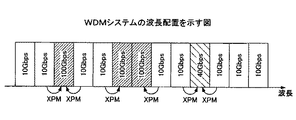
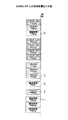
ビットレート10Gbps,40Gbps,100Gbpsの光信号が、図1に示すように波長配置されたWDMシステムでは、ビットレートの大きい40Gbps,100Gbpsの光信号が隣接するビットレートの小さい10Gbpsの光信号からXPMを受け、伝送劣化を引き起こしやすい。 In a WDM system in which optical signals with bit rates of 10 Gbps, 40 Gbps, and 100 Gbps are wavelength-arranged as shown in FIG. 1, an optical signal of 10 Gbps with a small bit rate adjacent to an optical signal with a high bit rate of 40 Gbps or 100 Gbps is used for XPM. It is easy to cause transmission degradation.
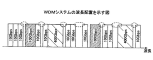
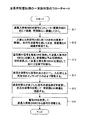
更に、波長の透過帯域幅を可変できるLCOS等のデバイスを使用したグリッドレス(Gridless)のネットワークにおいては、ビットレートによって占有する波長帯域が異なるため、各波長間の間隔はもはや等間隔ではなく、光信号のビットレートや変調方式に依存した、均一ではない波長配置になることが予想される。このようなグリッドレスネットワークにおいて、伝送パスの再構築や、光送受信器の入替えによるビットレートの変更を継続的に行った場合、図2に破線の楕円で示すように、波長配置に隙間ができるおそれがある。 Furthermore, in a gridless network using a device such as LCOS that can change the transmission bandwidth of the wavelength, the wavelength band occupied by the bit rate is different, so that the intervals between the wavelengths are no longer equal, It is expected that the wavelength arrangement is not uniform depending on the bit rate and modulation method of the optical signal. In such a gridless network, when the transmission path is reconstructed or the bit rate is changed by replacing the optical transceiver, a gap is formed in the wavelength arrangement, as shown by the dashed ellipse in FIG. There is a fear.
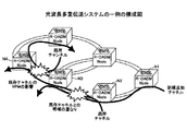
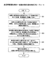
また、図3に示す光波長多重伝送システムにおいて、ノードN1でアッドし、ノードN2,N3を通してノードN4でドロップするチャネルを新規追加しようとした場合、光パスの途中であるノードN2,N3間及びノードN3,N4間で、新規追加チャネルと既存チャネルの一部光信号の帯域が重なるおそれがある。また、光信号の帯域が重ならずに光パスが通ったとしても、XPMの影響による劣化を受けるおそれがある。 Further, in the optical wavelength division multiplexing transmission system shown in FIG. 3, when adding a new channel to be added at the node N1 and dropped at the node N4 through the nodes N2 and N3, between the nodes N2 and N3 in the middle of the optical path and There is a possibility that the bands of the partially added optical signals of the newly added channel and the existing channel overlap between the nodes N3 and N4. Further, even if optical paths pass without overlapping optical signal bands, there is a risk of degradation due to the influence of XPM.
このような新規追加チャネルと既存チャネルの一部光信号の帯域の重なりやXPMによる劣化を低減するためには、波長再配置を行うことが必要になる。波長再配置を行う際には波長入替えが必要になる場合があり、従来は波長入替え時に光信号の瞬断が発生し、この光信号の瞬断時間が長いという問題があった。 In order to reduce the overlap between the bands of some optical signals of the newly added channel and the existing channel and the deterioration due to XPM, it is necessary to perform wavelength rearrangement. When performing the wavelength rearrangement, there is a case where it is necessary to change the wavelength. Conventionally, an instantaneous interruption of the optical signal occurs when the wavelength is changed, and there is a problem that the instantaneous interruption time of the optical signal is long.
開示の波長再配置方法は、波長再配置における光信号の瞬断時間を短縮化することを目的とする。 The disclosed wavelength rearrangement method aims to shorten the instantaneous interruption time of an optical signal in wavelength rearrangement.
開示の一実施形態による波長再配置方法は、光波長多重伝送システムの波長再配置方法において、
第1光送信器で第1波長の光信号に変換される第1チャネルの電気信号を、前記第1光送信器への供給から、前記第1波長とは異なる第2波長の光信号に変換する第2光送信器への供給に切替え、
前記第2光送信器の出力する前記第2波長の光信号を送信し、
第2チャネルの電気信号に基づいて第3光送信器で出力する光信号の波長を前記第1波長及び前記第2波長と異なる第3波長から前記第1波長方向に徐々にずらし前記第1波長にして送信し、
前記第1光送信器が前記第3波長の光信号を出力するよう設定し、
前記第1チャネルの電気信号を前記第2光送信器への供給から前記第1光送信器への供給に電気信号スイッチングで切替え、
前記第1光送信器の出力する前記第3波長の光信号を送信する。
A wavelength rearrangement method according to an embodiment of the disclosure is a wavelength rearrangement method of an optical wavelength division multiplexing transmission system,
The electrical signal of the first channel that is converted to the optical signal of the first wavelength by the first optical transmitter is converted from the supply to the first optical transmitter to the optical signal of the second wavelength different from the first wavelength. Switch to supply to the second optical transmitter,
Transmitting an optical signal of the second wavelength output from the second optical transmitter ;
The wavelength of the optical signal output from the third optical transmitter based on the electric signal of the second channel is gradually shifted from the third wavelength different from the first wavelength and the second wavelength in the first wavelength direction, and the first wavelength. And send
Setting the first optical transmitter to output an optical signal of the third wavelength;
The electrical signal of the first channel is switched from the supply to the second optical transmitter to the supply to the first optical transmitter by electrical signal switching.
The third optical signal output from the first optical transmitter is transmitted .
本実施形態によれば、波長再配置における光信号の瞬断時間を短縮化することができる。 According to this embodiment, the instantaneous interruption time of the optical signal in wavelength rearrangement can be shortened.
以下、図面に基づいて実施形態を説明する。 Embodiments will be described below with reference to the drawings.
<光波長多重伝送システム>
図4は光波長多重伝送システムの一実施形態の構成図を示す。図4において、ノードN1,N2,N3,N5それぞれの間は光ファイバで接続され、ノードN3,N4,N6,N5それぞれの間は光ファイバで接続されてネットワークを構成している。ノードN1〜N6それぞれは、光波長の変更や光パスの再構築が可能なR−OADM(Reconfigurable Optical Add/Drop Multiplexer)で構成されている。各ノードN1〜N6はネットワーク全体を監視制御するNMS(Network Management System)1と接続されている。なお、NMS1は全てのノードN1〜N6と接続されている必要はなく、NMS1は一部のノード(例えばN1)と接続されていれば、ノードN1からネットワークを介して他のノードN2〜N6と接続することができる。
<Optical wavelength multiplex transmission system>
FIG. 4 shows a configuration diagram of an embodiment of an optical wavelength division multiplexing transmission system. In FIG. 4, nodes N1, N2, N3, and N5 are connected by optical fibers, and nodes N3, N4, N6, and N5 are connected by optical fibers to form a network. Each of the nodes N1 to N6 includes an R-OADM (Reconfigurable Optical Add / Drop Multiplexer) that can change an optical wavelength and reconstruct an optical path. Each of the nodes N1 to N6 is connected to an NMS (Network Management System) 1 that monitors and controls the entire network. NMS1 does not need to be connected to all nodes N1 to N6. If NMS1 is connected to some nodes (for example, N1), NMS1 can be connected to other nodes N2 to N6 via the network from node N1. Can be connected.
<ノード装置の第1実施形態>
図5はノード装置の第1実施形態の構成図を示す。このノード装置はR−OADMであり、ノードN1〜N6として使用される。図5において、ポート#1から受信したWDM信号は光送受信部11−1で受信され、ポート#1に対応する多重分離部12−1のスプリッタ13(SPL)でパワー分岐される。分岐された光信号はポート#2〜#8それぞれに対応する送受信部の波長選択スイッチ(WSS:Wavelength Selected Switch)14に供給されると共に、受信用の波長選択スイッチ(WSS)16,17に供給される。同様に、ポート#8から受信したWDM信号は光送受信部11−8で増幅され、ポート#8に対応する多重分離部12−8のスプリッタ13でパワー分岐され、ポート#1〜#7それぞれに対応する送受信部の波長選択スイッチ14に供給されると共に、受信用の波長選択スイッチ18,19に供給される。
<First Embodiment of Node Device>
FIG. 5 shows a configuration diagram of the first embodiment of the node device. This node device is an R-OADM and is used as nodes N1 to N6. In FIG. 5, the WDM signal received from the
波長選択スイッチ16〜19は各波長を選択して波長毎に出力方路をスイッチングし、ナローバンドの光送受信器(NBO:Narrow Band Optics)21a,21b,21c,21d,21e等に供給する。光送受信器21a〜21eは光受信器として用いられ、光信号を電気信号に変換してスイッチファブリック(Switch Fabric)23に供給する。
The wavelength
スイッチファブリック23には光送受信器(NBO)21a〜21e,22a〜22e等と、光送受信器(CLT:Client unit)24a〜24e,25a〜25d等が接続されている。スイッチファブリック23は後述する管理部(MC:Management Complex)30の制御に従ってNBO21a〜21eの出力信号をCLT24a〜24d,NBO22a〜22eのいずれかに供給する。
Connected to the
光送受信器(CLT)24a〜24d,25a〜25d等はワイドバンドの光送受信器である。光送受信器24a〜24dはスイッチファブリック23から供給される電気信号を光信号に変換してクライアントに送信する。また、光送受信器25a〜25dはクライアントから受信したワイドバンドの光信号を電気信号に変換してスイッチファブリック23に供給する。スイッチファブリック23は光送受信器(CLT)25a〜25d等からの電気信号を光送受信器(NBO)22a〜22e等に供給する。
Optical transceivers (CLT) 24a to 24d, 25a to 25d, and the like are wideband optical transceivers. The
光送受信器(NBO)22a〜22eは光送信器として用いられ、スイッチファブリック23からの電気信号を光信号に変換して送信用の波長選択スイッチ31,32,33,34に供給する。波長選択スイッチ31,32で波長多重された光信号は多重分離部12−1の波長選択スイッチ14に供給されて、ポート#2〜#8からの光信号と波長多重される。その後、光送受信部11−1によりポート#1から送信される。波長選択スイッチ33,34で波長多重された光信号は多重分離部12−8の波長選択スイッチ14に供給されて、ポート#1〜#7からの光信号と波長多重される。その後、光送受信部11−8によりポート#8から送信される。
Optical transceivers (NBO) 22a to 22e are used as optical transmitters, convert electrical signals from the
ここで、波長選択スイッチ(WSS)14,16〜19,31〜34、光送受信器(NBO)21a〜21e,22a〜22eそれぞれは全てLCOSやTLD(Tunable Laser)等の波長可変デバイスを使用する。これらの波長可変デバイスは管理部(MC)30からの制御に従って発振又は送受信又は選択する波長を変化させることにより、CDC(Colorless Directionless Contentionless)機能におけるColorless機能を実現している。また、スイッチファブリック23によりDirectionless機能を実現している。なお、Colorlessとは出力光の波長を自由に変更できることを意味し、Directionlessとは出力光の方路を自由に変更できることを意味し、Contentionlessとは出力光において波長が衝突しないことを意味している。
Here, wavelength selective switches (WSS) 14, 16 to 19, 31 to 34, and optical transceivers (NBO) 21a to 21e, 22a to 22e all use wavelength variable devices such as LCOS and TLD (Tunable Laser). . These wavelength tunable devices realize a Colorless function in a CDC (Colorless Directional Contentionless) function by changing a wavelength to be oscillated, transmitted / received, or selected in accordance with control from the management unit (MC) 30. Further, the directionless function is realized by the
なお、波長選択スイッチ(WSS)14,16〜19,31〜34の代りに、光スイッチ(OXC:Optical Cross Connect Switch)と、波長毎に設けられる波長可変デバイスとしてのチューナブルフィルタ(TF:Tunable Filter)を用いても良い。 In place of the wavelength selective switches (WSS) 14, 16 to 19, 31 to 34, an optical switch (OXC: Optical Cross Connect Switch) and a tunable filter (TF: Tunable) as a wavelength tunable device provided for each wavelength. Filter) may be used.
<ガードバンド>
光信号間のXPMの影響をできるだけ抑えつつ、光波長帯域の有効利用を実現するためには、まず、ある最適なネットワークの波長の利用形態を定義し、それに合った光波長や光パスの選択を行う。更に、ネットワーク構築後に光波長の変更や光パスの再構築を行う際には、既存の光信号に影響を及ぼさず、かつ、変更の対象となる光信号についてもサービスを中断することのないインサービスで行う必要がある。
<Guard band>
In order to realize the effective use of the optical wavelength band while suppressing the influence of XPM between optical signals as much as possible, first define the usage form of a certain optimal network wavelength, and select the appropriate optical wavelength and optical path. I do. Furthermore, when the optical wavelength is changed or the optical path is reconstructed after the network is constructed, the existing optical signal is not affected and the service is not interrupted for the optical signal to be changed. Need to do in service.
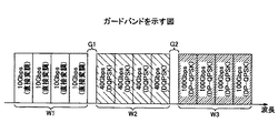
本実施形態では、図6に示すように、WDM伝送で使用する波長帯域をビットレート又は変調方式毎、又は、ビットレート及び変調方式毎に特定化し、特定化された各波長帯域の間に光信号の使用を許可しない帯域(ガードバンド)を設けることで、XPMの影響を回避する。 In this embodiment, as shown in FIG. 6, the wavelength band used in WDM transmission is specified for each bit rate or modulation method, or for each bit rate and modulation method, and light is transmitted between each specified wavelength band. By providing a band (guard band) that does not permit the use of a signal, the influence of XPM is avoided.
図6においては、第1の波長帯域W1にはビットレートが10Gbpsで直接変調された複数の光信号が波長配置されている。第2の波長帯域W2にはビットレートが40GbpsでDQPSK変調された複数の光信号が波長配置されている。また、第3の波長帯域W3にはビットレートが100GbpsでDP−QPSK変調された複数の光信号が波長配置されている。 In FIG. 6, a plurality of optical signals that are directly modulated at a bit rate of 10 Gbps are arranged in the first wavelength band W1. In the second wavelength band W2, a plurality of optical signals DQPSK modulated at a bit rate of 40 Gbps are arranged in wavelength. In the third wavelength band W3, a plurality of optical signals that are DP-QPSK modulated at a bit rate of 100 Gbps are arranged in wavelength.
そして、第1の波長帯域W1と第2の波長帯域W2の間には、特に第2の波長帯域W2の光信号が第1の波長帯域W1の光信号からXPMを受けない程度に十分な帯域幅のガードバンドG1が設けられている。また、第2の波長帯域W2と第3の波長帯域W3の間には、特に第3の波長帯域W3の光信号が第2の波長帯域W2の光信号からXPMを受けない程度に十分な帯域幅のガードバンドG2が設けられている。 The band between the first wavelength band W1 and the second wavelength band W2 is particularly sufficient to prevent the optical signal in the second wavelength band W2 from receiving XPM from the optical signal in the first wavelength band W1. A guard band G1 having a width is provided. Also, a band sufficient between the second wavelength band W2 and the third wavelength band W3, in particular, that the optical signal in the third wavelength band W3 does not receive XPM from the optical signal in the second wavelength band W2. A guard band G2 having a width is provided.
<スイッチファブリックによる波長の再配置>
XPMを避けるため、また、波長帯域の有効利用を行うために波長入替えが必要になる場合がある。この場合、光信号波長の変更を無瞬断で行うためには、使用していない空きの波長入替え用の光送受信器(NBO)を準備し、スイッチファブリック23において電気信号でスイッチングすることで1つの切替波長を波長入替え用の光送受信器(NBO)に回避させ、所望の信号を入替える。
<Relocation of wavelengths by switch fabric>
In order to avoid XPM and to make effective use of the wavelength band, it may be necessary to switch wavelengths. In this case, in order to change the optical signal wavelength without interruption, an unused optical transmitter / receiver (NBO) for exchanging the wavelength is prepared, and the
図7に示す波長配置では、10Gbpsで直接変調の信号(CH1)の波長λ1の隣に40GbpsでDQPSKの信号(CH2)の波長λ2が配置され、波長λ2の隣に10Gbpsで直接変調の信号(CH3)の波長λ3が配置され、波長λ3の隣に40GbpsでDQPSKの信号(CH4)の波長λ4が配置されている。このような波長配置で図4におけるノードN1からノードN2を経てノードN3にパスが設定されているものとして説明する。 In the wavelength arrangement shown in FIG. 7, the wavelength λ2 of the DQPSK signal (CH2) is arranged at 40 Gbps next to the wavelength λ1 of the signal (CH1) directly modulated at 10 Gbps, and the signal directly modulated at 10 Gbps (at 10 Gbps) ( The wavelength λ3 of CH3) is arranged, and the wavelength λ4 of the DQPSK signal (CH4) is arranged at 40 Gbps next to the wavelength λ3. The following description assumes that a path is set from the node N1 to the node N3 through the node N2 in FIG.
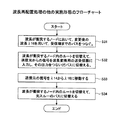
図8に波長再配置処理の一実施形態のフローチャートを示す。図8において、ステップS11でNMS1は波長入替え用NBOをビットレートと変調方式に応じて送信側及び受信側のノードに準備させる。
FIG. 8 shows a flowchart of an embodiment of the wavelength rearrangement process. In FIG. 8, in step S11, the
例えばノードN1では図5における光送受信器(CLT)25bからの信号(CH3)を光送受信器(NBO)22bで受信して波長λ3として波長選択スイッチ31に供給している場合、波長入替え用NBOとして波長λ5の光送受信器(NBO)22cを用意する。また、ノードN3では図5における光送受信器(NBO)21dが波長λ3の信号(CH3)を受信して光送受信器(CLT)24dに供給している場合、波長入替え用NBOとして波長λ5の光送受信器(NBO)21eを用意する。
For example, in the node N1, when the signal (CH3) from the optical transceiver (CLT) 25b in FIG. 5 is received by the optical transceiver (NBO) 22b and supplied to the wavelength
ステップS12でNMS1は入替える波長λ3と同じ光パスを他の波長(例えばλ5)で確保し、波長λ5の光パスに自己生成信号を流しておき、送信側のノードN1と受信側のノードN3との疎通を確認する。
In step S12, the
ステップS13でNMS1からの指示により送信側のノードN1のMC30はスイッチファブリック23にて光送受信器(CLT)25bからの信号(CH3)を光送受信器(NBO)22bへの供給から波長入替え用の光送受信器(NBO)22cへの供給に切替える指示を行う。受信側のノードN3では、波長λ3の入力光が断になった場合に波長λ5の入力光に自動的に切替える設定に予めしておけば、つまり、予め切替時の切替波長として波長入替え用のNBOとして光送受信器(NBO)21eを設定しておけばNMS1からの切替指示(又はOSCによる切替指示)により自動で切替える。これによって、図7の信号(CH3)の波長λ3は波長λ5に無瞬断で切替えられる。
In step S13, the MC 30 of the node N1 on the transmission side uses the
ここで、スイッチファブリック23にて光送受信器(CLT)25bからの信号(CH3)を光送受信器(NBO)22bへの供給から波長入替え用の光送受信器(NBO)22cへの供給に切替える場合、光送受信器(NBO)22b,22cそれぞれはデータバッファを有しており、光送受信器(CLT)25bからデータD1,D2が連続して出力される場合、データD1を光送受信器(NBO)22bに供給してバッファリングした後,データD2を光送受信器(NBO)22cに供給してバッファリングすることができ、光送受信器(NBO)22bがデータD1を含む光信号(λ3)を出力した後、光送受信器(NBO)22cがデータD2を含む光信号(λ5)を出力することで、受信側ではデータD1,D2を連続して得ることができ、無瞬断切替えが可能となる。
Here, the
次に、ステップS14でNMS1からの指示によりノードN1のMC30は波長選択スイッチ31が波長を切替えた光信号(λ3)の出力をオフするよう制御する。そして、MC30は入替える信号(CH2)の波長λ2をインサービスのままで図7における波長λ3の波長まで移動(変換)させる。上記の波長λ2を波長λ3の波長まで移動させる方法については後述する。
Next, in step S14, according to an instruction from the
ステップS15でNMS1からの指示によりノードN1のMC30は波長切替えが完了した信号(CH3)についての波長設定を図7における波長λ2に変更するよう光送受信器(NBO)22bの設定を行う。そして、自己生成信号を流して、受信側との疎通を確認する。
In step S15, in response to an instruction from the
ステップS16でNMS1からの指示により送信側のノードN1のMC30はスイッチファブリック23にて光送受信器(CLT)25bからの信号を元の光送受信器(NBO)22bに供給するよう切替指示を行う。
In step S16, the MC 30 of the transmission-side node N1 instructs the
このようにして、10Gbpsで直接変調の信号(CH3)を波長λ3から波長λ2に入替え、40GbpsでDQPSKの信号(CH2)を波長λ2から波長λ3に入替えることを無瞬断で行うことができる。 In this way, the direct modulation signal (CH3) at 10 Gbps can be switched from the wavelength λ3 to the wavelength λ2, and the DQPSK signal (CH2) at 40 Gbps can be switched from the wavelength λ2 to the wavelength λ3 without interruption. .
ところで、図7の例では40GbpsでDQPSKの信号(CH2)の波長λ2と、10Gbpsで直接変調の信号(CH3)の波長λ3のいずれか一方を波長入替え用の光送受信器(NBO)に回避させることになる。この波長入替え用のNBOを選択する際には、ビットレートの高いNBOと低いNBOいずれかを選択可能である。この場合は、ビットレートの低い信号(CH3)を優先するように、自動的にMC30が切替先を選択する。これは、ビットレートの低い信号の方が波長入替え用のNBOにおけるバッファ容量が少なくて済むためである。 By the way, in the example of FIG. 7, either the wavelength λ2 of the DQPSK signal (CH2) at 40 Gbps or the wavelength λ3 of the signal (CH3) directly modulated at 10 Gbps is caused to be avoided by the wavelength switching optical transceiver (NBO). It will be. When selecting this NBO for exchanging wavelengths, either an NBO with a high bit rate or an NBO with a low bit rate can be selected. In this case, the MC 30 automatically selects the switching destination so as to give priority to the signal (CH3) having a low bit rate. This is because a signal having a lower bit rate requires less buffer capacity in the NBO for exchanging wavelengths.
<波長の再配置の変形例>
図9に示す波長配置では、入替えを行おうとする40GbpsでDQPSKの信号(CH2)の波長λ2と、10Gbpsで直接変調の信号(CH3)の波長λ3との間に、100GbpsでDP−QPSKの信号の波長λ11が配置されている。このような波長配置で図4におけるノードN1からノードN2を経てノードN3にパスが設定されているものとして説明する。このような場合には、波長入替え用のNBOを2つ準備する。
<Modification of wavelength rearrangement>
In the wavelength arrangement shown in FIG. 9, the DP-QPSK signal at 100 Gbps is between the wavelength λ2 of the DQPSK signal (CH2) at 40 Gbps and the wavelength λ3 of the direct modulation signal (CH3) at 10 Gbps. Wavelength [lambda] 11 is arranged. The following description assumes that a path is set from the node N1 to the node N3 through the node N2 in FIG. In such a case, two NBOs for wavelength replacement are prepared.
図10に波長再配置処理の一実施形態の変形例のフローチャートを示す。図10において、ステップS21でNMS1は波長入替え用NBOをビットレートと変調方式に応じて送信側及び受信側のノードに準備させる。
FIG. 10 shows a flowchart of a modification of the embodiment of the wavelength rearrangement process. In FIG. 10, in step S21, the
ステップS22でNMS1は入替える波長λ2,λ3と同じ光パスを他の波長(例えばλ6,λ5)で確保し、波長λ6,λ5の光パスに自己生成信号を流しておき、送信側のノードN1と受信側のノードN3との疎通を確認する。
In step S22, the
ステップS23でNMS1からの指示により送信側のノードN1のMC30はスイッチファブリック23にて光送受信器(CLT)25bからの信号(CH3)を波長入替え用の光送受信器(NBO)22cに供給するよう切替指示を行い、同様にして信号(CH2)を波長入替え用の光送受信器(NBO)に供給するよう切替指示を行う。受信側のノードN3では、予めプロビジョニング時の切替波長として波長入替え用のNBOとして2つの光送受信器(NBO)21e等を設定しておけば自動で切替える。これによって、図9の信号(CH2,CH3)の波長λ2,λ3は波長λ6,λ5に無瞬断で切替えられる。
In step S23, the MC 30 of the node N1 on the transmission side supplies the signal (CH3) from the optical transceiver (CLT) 25b to the optical transceiver (NBO) 22c for wavelength switching in the
次に、ステップS24でNMS1からの指示によりノードN1のMC30は波長選択スイッチ31等が波長を切替えた波長λ2,λ3の出力をオフするよう制御する。そして、NMS1からの指示によりノードN1のMC30は波長切替えが完了した信号(CH2)についての波長設定を図9における波長λ3に変更し、信号(CH3)についての波長設定を波長λ2に変更するよう光送受信器(NBO)22b等の設定を行う。そして、自己生成信号を流して、受信側との疎通を確認する。
Next, in step S24, according to an instruction from the
ステップS25でNMS1からの指示により送信側のノードN1のMC30はスイッチファブリック23にて光送受信器(CLT)25b等からの信号を元の光送受信器(NBO)22b等に供給するよう切替指示を行う。
In step S25, in response to an instruction from the NMS1, the MC 30 of the transmission side node N1 instructs the
このようにして、10Gbpsで直接変調の信号(CH3)を波長λ3から波長λ2に入替え、40GbpsでDQPSKの信号(CH2)を波長λ2から波長λ3への入替えを無瞬断で行うことができる。 In this manner, the direct modulation signal (CH3) at 10 Gbps can be switched from the wavelength λ3 to the wavelength λ2, and the DQPSK signal (CH2) at 40 Gbps can be switched from the wavelength λ2 to the wavelength λ3 without interruption.
ところで、スイッチファブリック23において電気信号でスイッチングする際のバッファ容量に余裕がある場合は、できるだけビットレートの最も高い波長入替え用の光送受信器(NBO)を使用する。図9に示す10Gbps信号用の波長λ5の光送受信器(NBO)と、40Gbps信号用の波長λ6の光送受信器(NBO)の他に、100Gbps信号用の波長λ7の光送受信器(NBO)が波長入替え用のNBOとして使用可能である場合、100Gbps信号用の波長λ7の光送受信器(NBO)を波長入替え用のNBOとして選択する。そして、波長λ2の40GbpsでDQPSKの信号(CH2)と波長λ3の10Gbpsで直接変調の信号(CH3)を100Gbps信号用の波長λ7の光送受信器(NBO)に供給して波長λ7の光信号とすることができる。
By the way, when there is a margin in the buffer capacity when switching with an electrical signal in the
これにより、複数のNBOを準備する必要がなくなり、確保しなければならない帯域を減らすことができる。なお、10Gbps信号用の波長λ5と40Gbps信号用の波長λ6を合わせた波長帯域幅に比して、100Gbps信号用の波長λ7の波長帯域幅が小さくなる。 As a result, it is not necessary to prepare a plurality of NBOs, and the bandwidth that must be secured can be reduced. Note that the wavelength bandwidth of the wavelength λ7 for the 100 Gbps signal is smaller than the wavelength bandwidth of the wavelength λ5 for the 10 Gbps signal and the wavelength λ6 for the 40 Gbps signal.
上記方法により、40GbpsでDQPSKの信号(CH2)と10Gbpsで直接変調の信号(CH3)を100Gbps信号用の波長λ7を用いて伝送する場合、ビットレートが100Gbpsと高くなることにより、ビットレートが40Gbps又は10Gbps等の低い信号が確保できていた伝送性能を満足できなくなるおそれがある。これはビットレートが高くなるほど伝送距離が短くなるという特性があるためである。 When the DQPSK signal (CH2) at 40 Gbps and the direct modulation signal (CH3) at 10 Gbps are transmitted using the wavelength λ7 for the 100 Gbps signal by the above method, the bit rate is increased to 100 Gbps, so that the bit rate is 40 Gbps. Or, there is a possibility that the transmission performance in which a low signal such as 10 Gbps can be secured cannot be satisfied. This is because the transmission distance becomes shorter as the bit rate becomes higher.
このような場合は、NBOの出力としてビットレート可変機能を持つものを使用することで、波長入替え用の波長λ7の光信号を出力するNBOのビットレートを100Gbpsから50Gbpsに可変して信号(CH2,CH3)の伝送性能を向上させることができ、予備のNBOや波長帯域を有効に使用することが可能になる。 In such a case, by using an NBO output that has a variable bit rate function, the bit rate of the NBO that outputs the optical signal having the wavelength λ7 for wavelength switching is changed from 100 Gbps to 50 Gbps, and the signal (CH2 , CH3) transmission performance can be improved, and spare NBO and wavelength bands can be used effectively.
上記実施形態は、ネットワーク側の波長の入替えのみではなく、クライアント側の信号をネットワーク側の信号に束ねる際に、より効率よく、収容性の高い多重化を行うために、一度空きポートの波長に退避させて、波長の再入替えを行う際にも有効な方法となる。例えば10系統の10Gbpsのクライアント信号が10個の光送受信器(CLT)25a等に供給され、スイッチファブリック23で10個の10Gbps信号用の光送受信器(NBO)22aに供給され、10波長で同一パスに伝送されている場合を考える。この場合、スイッチファブリック23において、10個の光送受信器(CLT)25a等を1個の100Gbps信号用の光送受信器(NBO)に供給して100Gbps信号用の波長で伝送することができる。これにより、多くのNBOを準備する必要がなくなり、確保しなければならない帯域を減らすことができる。
In the above embodiment, not only the wavelength on the network side is replaced, but also when the client side signal is bundled with the network side signal, the wavelength of the empty port is once set in order to perform more efficient and high capacity multiplexing. This is also an effective method for saving and performing wavelength re-exchange. For example, 10 systems of 10 Gbps client signals are supplied to 10 optical transceivers (CLT) 25 a and the like, and are supplied to 10 optical transceivers (NBO) 22 a for 10 Gbps signals by the
<ノード装置の第2実施形態>
図11はノード装置の第2実施形態の構成図を示す。このノード装置は設定追従モードに対応した構成のR−OADMであり、ノードN1〜N6として使用される。図11において、ポート#1から受信したWDM信号は光送受信部41−1で受信され、ポート#1に対応する多重分離部42−1のスプリッタ43でパワー分岐され、ポート#2〜#8それぞれに対応する送受信部の波長選択スイッチ(WSS)44に供給されると共に、多重分離部42−1内のスプリッタ45でパワー分岐されて受信用の波長選択スイッチ(WSS)47,48に供給される。
<Second Embodiment of Node Device>
FIG. 11 shows a configuration diagram of a second embodiment of the node device. This node device is an R-OADM having a configuration corresponding to the setting tracking mode, and is used as the nodes N1 to N6. In FIG. 11, the WDM signal received from the
同様に、ポート#8から受信したWDM信号は光送受信部41−8で増幅され、ポート#8に対応する多重分離部42−8のスプリッタ43でパワー分岐され、ポート#1〜#7それぞれに対応する送受信部の波長選択スイッチ44に供給されると共に、多重分離部42−8内のスプリッタ45でパワー分岐されて受信用の波長選択スイッチ(WSS)47,48に供給される。
Similarly, the WDM signal received from the
波長選択スイッチ47の出力する多重光信号はスプリッタ(SPL)49においてパワー分岐されて波長選択スイッチ(WSS)51,52に供給される。波長選択スイッチ51,52は各波長を選択して波長毎に出力方路をスイッチングし、光送受信器であるトランスポンダ(TP)53a〜53d等に供給する。トランスポンダ53a〜53dは光信号を電気信号に変換してフレーミングを行い、この電気信号をワイドバンドの光信号に変換してクライアントに送信する。
The multiplexed optical signal output from the wavelength
同様に、波長選択スイッチ48の出力する多重光信号はスプリッタ54においてパワー分岐されて波長選択スイッチ(WSS)55,56に供給される。波長選択スイッチ55,56は各波長を選択して波長毎に出力方路をスイッチングし、光送受信器であるトランスポンダ(TP)57a〜57d等に供給する。トランスポンダ57a〜57dはナローバンドの光信号を電気信号に変換してフレーミングを行い、この電気信号をワイドバンドの光信号に変換してクライアントに送信する。
Similarly, the multiplexed optical signal output from the wavelength
トランスポンダ(TP)58a〜58d等は光送受信器であり、クライアントから受信したワイドバンドの光信号を電気信号に変換してフレーミングを行い、この電気信号をナローバンドの光信号に変換して波長選択スイッチ(WSS)59,60に供給する。波長選択スイッチ59,60は各波長の光信号を多重し、波長選択スイッチ59,60の出力する光信号はカプラ(CPL)61で合波されて送信用の波長選択スイッチ(WSS)62に供給される。波長選択スイッチ62は各波長を選択して波長毎に出力方路をスイッチングし、多重分離部42−1〜42−8のカプラ(CPL)46に供給する。
Transponders (TP) 58a to 58d and the like are optical transceivers, which convert a wideband optical signal received from a client into an electrical signal, perform framing, convert the electrical signal into a narrowband optical signal, and select a wavelength selection switch. (WSS) 59, 60. The wavelength
同様に、トランスポンダ(TP)64a〜64d等は光送受信器であり、クライアントから受信したワイドバンドの光信号を電気信号に変換してフレーミングを行い、この電気信号をナローバンドの光信号に変換して波長選択スイッチ(WSS)65,66に供給する。波長選択スイッチ65,66は各波長の光信号を多重し、波長選択スイッチ65,66の出力する光信号はカプラ(CPL)67で合波されて送信用の波長選択スイッチ(WSS)68に供給される。波長選択スイッチ68は各波長を選択して波長毎に出力方路をスイッチングし、多重分離部42−1〜42−8のカプラ(CPL)46に供給する。
Similarly, transponders (TP) 64a to 64d are optical transceivers, which convert a wideband optical signal received from a client into an electrical signal, perform framing, and convert the electrical signal into a narrowband optical signal. This is supplied to wavelength selective switches (WSS) 65 and 66. The wavelength
多重分離部42−1〜42−8のカプラ46で合波された光信号は波長選択スイッチ44に供給されて、ポート#1〜#8からの光信号と波長多重される。その後、光送受信部41−1〜41−8それぞれを通してポート#1〜#8から送信される。
The optical signals combined by the
ここで、波長選択スイッチ(WSS)44,47,48,51,52,55,56,59,60,62,65,66,68、トランスポンダ58a〜58d,64a〜64dそれぞれは全てLCOSやTLD等の波長可変デバイスを使用する。また、トランスポンダ53a〜53d,57a〜57dのコヒーレント受信器で用いる局部発振光の生成部も波長可変デバイスを使用する。
Here, wavelength selective switches (WSS) 44, 47, 48, 51, 52, 55, 56, 59, 60, 62, 65, 66, 68,
なお、波長選択スイッチ(WSS)44,47,48,51,52,55,56,59,60,62,65,66,68の代りに、光スイッチ(OXC)と、波長毎に設けられる波長可変デバイスとしてのチューナブルフィルタ(TF)を用いても良い。 Instead of the wavelength selective switch (WSS) 44, 47, 48, 51, 52, 55, 56, 59, 60, 62, 65, 66, 68, an optical switch (OXC) and a wavelength provided for each wavelength. A tunable filter (TF) as a variable device may be used.
これらの波長可変デバイスは管理部(MC)70からの制御に従って発振又は送受信又は選択する波長を変化させることにより、CDC(Colorless Directionless Contentionless)機能におけるColorless機能を実現している。また、各多重分離部内のスプリッタ45の出力信号を受信用の波長選択スイッチ47,48に供給して波長選択し、送信用の波長選択スイッチ62,68で波長選択を行った信号を各多重分離部内のカプラ46に供給することでDirectionless機能を実現している。
These wavelength variable devices realize a Colorless function in a CDC (Colorless Directional Contentionless) function by changing a wavelength to be oscillated or transmitted / received or selected according to control from the management unit (MC) 70. Further, the output signal of the
また、管理部(MC)70はNMS1から波長切替えを行う光信号や切替え後の波長の制御情報を指示される。光送受信部41−1〜41−8には、監視制御情報をネットワークの上流から下流に受け渡すためのOSC(Optical Supervisory Channel)信号を送受信するためのOSC送受信部71−1〜71−8が設けられている。図11でポート#8側に下流のノードが接続され、ポート#1側に上流のノードが接続されているものとした場合、管理部70はNMS1からの制御情報をOSC送受信部71−8に供給し、OSC送受信部71−8は上記制御情報をOSC信号に挿入して下流のノード装置に送信する。また、下流のノード装置ではOSC送受信部71−1でOSC信号から上記制御情報を抽出して管理部70に供給する。
In addition, the management unit (MC) 70 is instructed by the
<変形例>
図12はノード装置の第2実施形態の変形例の構成図を示す。このノード装置は自動追従モードに対応した構成のR−OADMであり、ノードN1〜N6として使用される。図12において図11と異なる構成は、光モニタ(OCM:Optical Channel Monitor)72〜76を設けている点である。光モニタ72は波長選択スイッチ44の後段に設けられ、光モニタ73,74はカプラ46,67の後段に設けられ、光モニタ75,76は波長選択スイッチ47,51の後段に設けられており、各光モニタ72〜76で計測された光信号の中心波長等は管理部(MC)70に供給される。
<Modification>
FIG. 12 shows a configuration diagram of a modification of the second embodiment of the node device. This node device is an R-OADM having a configuration corresponding to the automatic tracking mode, and is used as the nodes N1 to N6. 12 is different from FIG. 11 in that optical monitors (OCM: Optical Channel Monitor) 72 to 76 are provided. The
なお、図12では図示していないが、多重分離部42−1の波長選択スイッチ44、カプラ46、カプラ61、波長選択スイッチ52,48,55,56それぞれの後段に光モニタ(OCM)を設けても良い。
Although not shown in FIG. 12, an optical monitor (OCM) is provided in the subsequent stage of each of the
<インサービスでの信号波長変更>
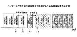
波長再配置処理におけるステップS14で光信号の波長を変更する場合や、ネットワークの構築後にビットレートの変更や光パスの再配置などにより波長帯域にできた隙間を埋めて新たな信号帯域を作り出す場合には、極力、無瞬断で信号波長を切替える。例えば図13では、10Gbpsで直接変調の信号(CH1)の波長λ1から帯域を空けて10Gbpsで直接変調の信号(CH3)の波長λ2が配置され、波長λ2から帯域を空けて40GbpsでDQPSKの信号(CH2)の波長λ3が配置され、波長λ3から帯域を空けて40GbpsでDQPSKの信号(CH4)の波長λ4が配置されている。この場合、波長λ2を波長λ1方向にずらして波長λ1に隣接させ、同様に、波長λ3を波長λ4方向にずらして波長λ4に隣接させ、波長λ2,λ3間の波長帯域を大きく空けることで新たな信号帯域を作り出すことができる。
<In-service signal wavelength change>
When the wavelength of the optical signal is changed in step S14 in the wavelength rearrangement processing, or when a new signal band is created by filling a gap formed in the wavelength band by changing the bit rate or rearranging the optical path after the network is constructed. If possible, switch the signal wavelength without interruption. For example, in FIG. 13, a wavelength λ2 of a signal (CH3) directly modulated at 10 Gbps is allocated from a wavelength λ1 of a signal (CH1) directly modulated at 10 Gbps, and a DQPSK signal is spaced at 40 Gbps from a wavelength λ2. The wavelength λ3 of (CH2) is arranged, and the wavelength λ4 of the DQPSK signal (CH4) is arranged at 40 Gbps with a band from the wavelength λ3. In this case, the wavelength λ2 is shifted in the wavelength λ1 direction so as to be adjacent to the wavelength λ1, and similarly, the wavelength λ3 is shifted in the wavelength λ4 direction so as to be adjacent to the wavelength λ4. A simple signal band.
この場合、波長を切替える又はずらす光信号及び隣接する波長の光信号に瞬断や劣化が起きないようにしながら波長を切替える構成について説明する。 In this case, a configuration will be described in which the wavelength is switched while preventing an instantaneous interruption or deterioration in the optical signal for switching or shifting the wavelength and the optical signal of the adjacent wavelength.
<設定追従モード>
図11において、NMS1では図4に示すネットワークにおける波長配置及びパス設定情報を集約している。NMS1により波長切替を行う光信号に対して切替後の波長である移動先波長を光パスの通る各ノードに設定する。送信側ノードでは、管理部70から例えばトランスポンダ64d,波長選択スイッチ(WSS)66,68,多重分離部42−8の波長選択スイッチ(WSS)44に現在の設定波長と波長変更量を通知して、光信号の劣化(又はFECのエラー訂正数)によるペナルティが発生しない程度に(例えば1GHzずつ)、中心波長あるいは帯域を切替後の波長方向にずらし、ずらした信号波長の情報をノードの管理部70からOSC送受信部71−8に供給し、OSC信号を使用して下流のノードに通知する。
<Setting tracking mode>
In FIG. 11,
下流のノードは、上流から受信したOSC信号の信号波長の情報により、管理部70は波長選択スイッチ(WSS)47,51,例えばトランスポンダ53aに現在の設定波長と波長変更量を通知して、中心波長あるいは帯域をずらして行く。
Based on the signal wavelength information of the OSC signal received from the upstream, the downstream node notifies the wavelength selective switch (WSS) 47, 51, for example, the
更に、トランスポンダとしてビットレート可変送受信器を使用しており、信号のビットレートが変わる場合は、NMS1あるいは管理部70により下流のノードに信号のビットレートを通知し、該当する波長選択スイッチ(WSS)の帯域幅を変更する。
Furthermore, when a bit rate variable transceiver is used as a transponder and the bit rate of the signal changes, the bit rate of the signal is notified to the downstream node by the
<自動追従モード>
図12において、NMS1では図4に示すネットワークにおける波長配置及びパス設定情報を集約している。NMS1により波長切替を行う光信号に対して切替後の波長である移動先波長を光パスの通る各ノードに設定する。送信側ノードでは、管理部70から例えばトランスポンダ64d,波長選択スイッチ(WSS)66,68,多重分離部42−8の波長選択スイッチ(WSS)44に現在の設定波長と波長変更量を通知して、光モニタ(OCM)72,73,74でモニタされた中心波長を監視しながら中心波長あるいは帯域を切替後の波長方向にずらす。
<Automatic tracking mode>
In FIG. 12, the
下流のノードは、光モニタ(OCM)75,76でモニタされた中心波長の情報に応じて管理部70は波長選択スイッチ(WSS)47,51,例えばトランスポンダ53aに現在の設定波長と波長変更量を通知して、中心波長あるいは帯域をずらして行く。
In the downstream node, according to the information on the center wavelength monitored by the optical monitors (OCM) 75 and 76, the
更に、トランスポンダにビットレート可変送受信器を使用しており、信号のビットレートが変わる場合は、光モニタ(OCM)72〜76で該当波長のスペクトルの帯域幅をモニタし、管理部70により自動的に該当する波長選択スイッチ(WSS)の帯域を変更する。
Furthermore, when a variable bit rate transceiver is used for the transponder and the bit rate of the signal changes, the bandwidth of the spectrum of the corresponding wavelength is monitored by the optical monitor (OCM) 72 to 76, and the
<アラーム、モニタリング方式>
ところで、将来的にビットレート増加の可能性がある場合は、ビットレート増加分の帯域をガードバンドとして確保するように、NMS1から、あるいはOSC信号を用いて各ノードに通知する。ネットワーク内のいずれかのノードでガードバンドに含まれる波長を使用しようとした場合は、これを検出したノードからNMS1にアラーム(警報)をあげる。
<Alarm, monitoring method>
By the way, when there is a possibility of an increase in the bit rate in the future, the node is notified from the
また、波長を変更する先の受信側ノードで、移動先波長を他のパスで使用していると、光信号が衝突してしまうため、予め移動先波長をネットワーク全体に通知し、既に移動先波長を使用している区間がある場合はアラームをあげる。なお、このアラームはNMS1で行ってもよい。
In addition, if the destination wavelength of the destination node that changes the wavelength is using the destination wavelength on another path, the optical signal will collide. Raise an alarm if there is a section that uses the wavelength. This alarm may be performed by the
また、各ノードの管理部70は、移動先波長あるいは隣接波長の劣化(又はFECのエラー訂正数)の状況を監視し、移動先波長あるいは隣接波長の劣化(又はFECのエラー訂正数)が所定の閾値を超えてアラームがあがった場合は、波長切替動作を停止する。
In addition, the
<既存信号を通過する(またぐ)波長切替>
図14に示す波長配置において、既存の信号波長λ15を通過する(またぐ)形で波長λ14を波長λ16に切替える場合について考える。例えば図15に示すネットワークにおいて、既存の信号(波長λ15)はノードN2からノードN3を通しノードN4に至るパスである。そして、波長λ14はノードN1からノードN2,N3を通しノードN4に至るパスである。このような場合に光信号の瞬断(50ms以内)が許容される場合は、図10の波長再配置処理を使用する以外にも、以下の方法により、波長変更の際に各ノードに1個の波長変換用の光送受信器(NBO)を準備しておくだけで、光送受信器(NBO)の波長変更速度よりも十分短い瞬断時間での切替えが可能になる。なお、この実施形態では、図5に示すようにスイッチファブリック23を有するノード装置が必要となる。
<Wavelength switching through existing signals>
Consider the case where the wavelength λ14 is switched to the wavelength λ16 in such a manner as to pass through the existing signal wavelength λ15 in the wavelength arrangement shown in FIG. For example, in the network shown in FIG. 15, the existing signal (wavelength λ15) is a path from the node N2 through the node N3 to the node N4. The wavelength λ14 is a path from the node N1 through the nodes N2 and N3 to the node N4. In such a case, when instantaneous interruption (within 50 ms) of the optical signal is allowed, in addition to using the wavelength rearrangement processing of FIG. By simply preparing an optical transmitter / receiver (NBO) for wavelength conversion, it is possible to perform switching in an instantaneous interruption time sufficiently shorter than the wavelength change speed of the optical transmitter / receiver (NBO). In this embodiment, a node device having the
図16に波長再配置処理の他の実施形態のフローチャートを示す。図16おいて、ステップS31では、波長λ14を波長λ16に変更する際に波長λ15と衝突するノードN2において、変更後の波長λ16を用いて受信端のノードN4までのパス(N2,N3,N4)を設定する。 FIG. 16 shows a flowchart of another embodiment of the wavelength rearrangement process. In FIG. 16, in step S31, at the node N2 that collides with the wavelength λ15 when the wavelength λ14 is changed to the wavelength λ16, the path (N2, N3, N4) to the node N4 at the receiving end using the changed wavelength λ16. ) Is set.
ステップS32では、前記衝突するノードN2において、波長λ14の光信号に対するルートを、多重分離部12−1のスプリッタ13から多重分離部12−8の波長選択スイッチ(WSS)14への供給するルートから、多重分離部12−1のスプリッタ13から波長選択スイッチ(WSS)16,17を経て例えば光送受信器(NBO)21bに供給するよう切替える。更に、光送受信器21bで波長λ14の光信号を電気信号に変換しスイッチファブリック23で波長λ16の光信号を生成する例えば光送受信器(NBO)22dに供給する。これにより、波長λ14の光信号は波長λ16に変換され、波長選択スイッチ(WSS)33,14を通り、ステップS31で設定されたパスに切替えて載せる。この際に50ms以内の瞬断が発生する。
In step S32, in the colliding node N2, the route for the optical signal of wavelength λ14 is supplied from the
ステップS33で、送信元のノードN1において、波長λ14の光信号を波長λ16に変更する。この波長変更には前述の設定追従モード又は自動追従モードを用いてノードN2,N3,N4における波長λ14の光信号を波長λ16に変更する。 In step S33, the optical signal having the wavelength λ14 is changed to the wavelength λ16 at the source node N1. For this wavelength change, the optical signal having the wavelength λ14 at the nodes N2, N3, and N4 is changed to the wavelength λ16 by using the setting tracking mode or the automatic tracking mode.
ステップS34で、前記衝突するノードN2において、波長λ16の光信号に対するルートを多重分離部12−1のスプリッタ13から多重分離部12−8の波長選択スイッチ(WSS)14に供給し、波長選択スイッチ(WSS)14では多重分離部12−1のスプリッタ13からの光信号を選択して出力するように切替える。この際に50ms以内の瞬断が発生する。
In step S34, at the colliding node N2, a route for the optical signal having the wavelength λ16 is supplied from the
このようにして、さまざまなビットレートや変調方式が混在する際の、XPMによる伝送品質の劣化を防ぐことが可能になる。また、光信号が瞬断することのないインサービスで波長変更を行うことにより、WDM信号の帯域の有効利用と柔軟なネットワーク設計が可能になる。また、波長変更のための設備を最小限にすることが可能になり、より短い時間での波長変更が可能になる。
(付記1)
光波長多重伝送システムの波長再配置方法において、
第1光送信器で第1波長の光信号に変換される第1チャネルの電気信号を、前記第1光送信器への供給から、前記第1波長とは異なる第2波長の光信号に変換する第2光送信器への供給に切替え、
前記第2光送信器の出力する前記第2波長の光信号を送信する
ことを特徴とする波長再配置方法。
(付記2)
付記1記載の波長再配置方法において、
第2チャネルの電気信号に基づいて第3光送信器で出力する光信号の波長を前記第3波長から前記第1波長方向に徐々にずらし前記第1波長にして送信する
ことを特徴とする波長再配置方法。
(付記3)
付記2記載の波長再配置方法において、
前記第1光送信器が前記第3波長の光信号を出力するよう設定し、
前記第1チャネルの電気信号を前記第2光送信器への供給から前記第1光送信器への供給に電気信号スイッチングで切替え、
前記第1光送信器の出力する前記第3波長の光信号を送信する
ことを特徴とする波長再配置方法。
(付記4)
付記1記載の波長再配置方法において、
第3光送信器で第3波長の光信号に変換される第2チャネルの電気信号を、前記第3光送信器への供給から、前記第1乃至第3波長とは異なる第4波長の光信号に変換する第4光送信器への供給に切替え、
前記第4光送信器の出力する前記第4波長の光信号を送信する
ことを特徴とする波長再配置方法。
(付記5)
付記4記載の波長再配置方法において、
前記第1光送信器が前記第3波長の光信号を出力し、かつ、前記第3光送信器が前記第1波長の光信号を出力するよう設定し、
前記第1チャネルの電気信号を前記第2光送信器への供給から前記第1光送信器への供給に電気信号スイッチングで切替え、かつ、前記第2チャネルの電気信号を前記第4光送信器への供給から前記第3光送信器への供給に電気信号スイッチングで切替え、
前記第1光送信器の出力する前記第3波長の光信号を送信し、前記第3光送信器の出力する前記第1波長の光信号を送信する
ことを特徴とする波長再配置方法。
(付記6)
光波長多重伝送システムの波長再配置方法において、
第1波長の光信号を受信して第1チャネルの電気信号に変換する第1光受信器と、前記第1チャネルの電気信号を前記第1波長とは異なる第2波長の光信号に変換する第1光送信器を用意し、
ネットワークから受信した前記第1波長の光信号を前記第1光受信器に供給するよう波長選択光スイッチングで切替え、
前記第1光受信器で変換した前記第1チャネルの電気信号を前記第1光送信器に供給するよう電気信号スイッチングで切替え、
前記第1光送信器の出力する前記第2波長の光信号を送信し、
前記ネットワークから前記第1チャネルの電気信号を変換した前記第2波長の光信号を受信した後、前記第1光送信器の出力する前記第2波長の光信号を前記ネットワークから受信した前記第2波長の光信号に波長選択光スイッチングで切替えて前記ネットワークに送信する
ことを特徴とする波長再配置方法。
(付記7)
光波長多重伝送システムのノード装置において、
第1チャネルの電気信号を第1波長の光信号に変換する第1光送信器と、
前記第1チャネルの電気信号を前記第1波長とは異なる第2波長の光信号に変換する第2光送信器と、
前記第1チャネルの電気信号を前記第1光送信器への供給から前記第2光送信器への供給に切替える電気信号スイッチング部と、
前記第1光送信器の出力する前記第1波長の光信号又は前記第2光送信器の出力する前記第2波長の光信号を送信する送信部と、
を有することを特徴とするノード装置。
(付記8)
付記7記載のノード装置において、
第2チャネルの電気信号を所定波長の光信号に変換して出力する波長可変素子の第3光送信器を有し、
前記第3光送信器の出力する光信号を第3波長から前記第1波長方向に徐々にずらし前記第1波長にする
ことを特徴とするノード装置。
(付記9)
付記8記載のノード装置において、
前記第1光送信器は、波長可変素子であり、前記第1光送信器が前記第3波長の光信号を出力するよう設定し、
前記電気信号スイッチング部は、前記第1チャネルの電気信号を前記第2光送信器への供給から前記第1光送信器への供給に切替え、
前記送信部は、前記第1光送信器の出力する前記第3波長の光信号を送信する
ことを特徴とするノード装置。
(付記10)
付記7記載のノード装置において、
第2チャネルの電気信号を前記第3波長の光信号に変換する第3光送信器と、
前記第2チャネルの電気信号を前記第1乃至第3波長とは異なる第4波長の光信号に変換する第4光送信器を有し、
前記電気信号スイッチング部は、前記第2チャネルの電気信号を前記第3光送信器への供給から前記第4光送信器への供給に切替え、
前記送信部は、前記第4光送信器の出力する前記第4波長の光信号を送信する
ことを特徴とするノード装置。
(付記11)
付記10記載のノード装置において、
前記第1光送信器と前記第3光送信器は、波長可変素子であり、前記第1光送信器が前記第3波長の光信号を出力し、かつ、前記第3光送信器が前記第1波長の光信号を出力するよう設定し、
前記電気信号スイッチング部は、前記第1チャネルの電気信号を前記第2光送信器への供給から前記第1光送信器への供給に切替え、かつ、前記第2チャネルの電気信号を前記第4光送信器への供給から前記第3光送信器への供給に切替え、
前記送信部は、前記第1光送信器の出力する前記第3波長の光信号を送信し、前記第3光送信器の出力する前記第1波長の光信号を送信する
ことを特徴とするノード装置。
(付記12)
光波長多重伝送システムのノード装置において、
第1波長の光信号を受信して第1チャネルの電気信号に変換する第1光受信器と、
前記第1チャネルの電気信号を前記第1波長とは異なる第2波長の光信号に変換する第1光送信器と、
ネットワークから受信した前記第1波長の光信号を前記第1光受信器への供給に切替える波長選択光スイッチング部と、
前記第1光受信器で変換した前記第1チャネルの電気信号を前記第1光送信器への供給に切替える電気信号スイッチング部と、
前記第1光送信器の出力する前記第2波長の光信号を送信する送信部とを有し、
前記波長選択光スイッチング部は、前記ネットワークから前記第1チャネルの電気信号を変換した前記第2波長の光信号を受信した後、前記第1光送信器の出力する前記第2波長の光信号を前記ネットワークから受信した前記第2波長の光信号に切替えて前記ネットワークに送信する
ことを特徴とするノード装置。
In this way, it is possible to prevent deterioration in transmission quality due to XPM when various bit rates and modulation methods are mixed. In addition, by changing the wavelength in-service where the optical signal is not interrupted, effective use of the bandwidth of the WDM signal and flexible network design are possible. Further, it becomes possible to minimize the equipment for changing the wavelength, and the wavelength can be changed in a shorter time.
(Appendix 1)
In the wavelength relocation method of the optical wavelength division multiplexing system,
The electrical signal of the first channel that is converted to the optical signal of the first wavelength by the first optical transmitter is converted from the supply to the first optical transmitter to the optical signal of the second wavelength different from the first wavelength. Switch to supply to the second optical transmitter,
A wavelength rearrangement method for transmitting an optical signal of the second wavelength output from the second optical transmitter.
(Appendix 2)
In the wavelength relocation method according to
The wavelength is characterized in that the wavelength of the optical signal output from the third optical transmitter based on the electric signal of the second channel is gradually shifted from the third wavelength in the first wavelength direction and transmitted to the first wavelength. Relocation method.
(Appendix 3)
In the wavelength relocation method described in
Setting the first optical transmitter to output an optical signal of the third wavelength;
The electrical signal of the first channel is switched from the supply to the second optical transmitter to the supply to the first optical transmitter by electrical signal switching.
A wavelength rearrangement method, comprising: transmitting an optical signal of the third wavelength output from the first optical transmitter.
(Appendix 4)
In the wavelength relocation method according to
A light of a fourth wavelength different from the first to third wavelengths is supplied from the supply of the second channel electrical signal converted into an optical signal of the third wavelength by the third optical transmitter to the third optical transmitter. Switch to supply to the fourth optical transmitter to convert to signal,
A wavelength rearrangement method comprising transmitting an optical signal having the fourth wavelength output from the fourth optical transmitter.
(Appendix 5)
In the wavelength relocation method described in appendix 4,
The first optical transmitter is configured to output the optical signal of the third wavelength, and the third optical transmitter is configured to output the optical signal of the first wavelength;
The electric signal of the first channel is switched from the supply to the second optical transmitter to the supply to the first optical transmitter by electric signal switching, and the electric signal of the second channel is switched to the fourth optical transmitter. Switching from supply to supply to the third optical transmitter by electrical signal switching,
A wavelength rearrangement method comprising transmitting an optical signal of the third wavelength output from the first optical transmitter and transmitting an optical signal of the first wavelength output from the third optical transmitter.
(Appendix 6)
In the wavelength relocation method of the optical wavelength division multiplexing system,
A first optical receiver that receives an optical signal of a first wavelength and converts it into an electric signal of a first channel, and converts the electric signal of the first channel into an optical signal of a second wavelength different from the first wavelength Prepare the first optical transmitter,
Switched by wavelength selective optical switching to supply the first optical signal received from the network to the first optical receiver,
The electric signal of the first channel converted by the first optical receiver is switched by electric signal switching so as to be supplied to the first optical transmitter.
Transmitting the optical signal of the second wavelength output from the first optical transmitter;
After receiving the optical signal of the second wavelength obtained by converting the electrical signal of the first channel from the network, the second optical signal of the second wavelength output from the first optical transmitter is received from the network. A wavelength rearrangement method comprising: switching to an optical signal having a wavelength by wavelength selective optical switching and transmitting to the network.
(Appendix 7)
In the node equipment of the optical wavelength division multiplexing transmission system,
A first optical transmitter for converting an electric signal of the first channel into an optical signal of a first wavelength;
A second optical transmitter for converting the electric signal of the first channel into an optical signal having a second wavelength different from the first wavelength;
An electrical signal switching unit for switching the electrical signal of the first channel from the supply to the first optical transmitter to the supply to the second optical transmitter;
A transmitter that transmits the optical signal of the first wavelength output from the first optical transmitter or the optical signal of the second wavelength output from the second optical transmitter;
A node device comprising:
(Appendix 8)
In the node device according to
A third optical transmitter of a wavelength tunable element that converts the electric signal of the second channel into an optical signal of a predetermined wavelength and outputs the optical signal;
A node device characterized in that an optical signal output from the third optical transmitter is gradually shifted from a third wavelength in the first wavelength direction to the first wavelength.
(Appendix 9)
In the node device according to
The first optical transmitter is a wavelength variable element, and the first optical transmitter is set to output an optical signal of the third wavelength;
The electrical signal switching unit switches the electrical signal of the first channel from supply to the second optical transmitter to supply to the first optical transmitter,
The node device transmits the optical signal of the third wavelength output from the first optical transmitter.
(Appendix 10)
In the node device according to
A third optical transmitter for converting an electric signal of the second channel into an optical signal of the third wavelength;
A fourth optical transmitter for converting the electric signal of the second channel into an optical signal having a fourth wavelength different from the first to third wavelengths;
The electrical signal switching unit switches the electrical signal of the second channel from supply to the third optical transmitter to supply to the fourth optical transmitter,
The node device transmits the optical signal of the fourth wavelength output from the fourth optical transmitter.
(Appendix 11)
In the node device according to attachment 10,
The first optical transmitter and the third optical transmitter are wavelength tunable elements, the first optical transmitter outputs an optical signal of the third wavelength, and the third optical transmitter is the first optical transmitter. Set to output an optical signal of one wavelength,
The electrical signal switching unit switches the electrical signal of the first channel from the supply to the second optical transmitter to the supply to the first optical transmitter, and the electrical signal of the second channel is changed to the fourth signal. Switching from the supply to the optical transmitter to the supply to the third optical transmitter,
The transmission unit transmits the optical signal of the third wavelength output from the first optical transmitter, and transmits the optical signal of the first wavelength output from the third optical transmitter. apparatus.
(Appendix 12)
In the node equipment of the optical wavelength division multiplexing transmission system,
A first optical receiver that receives an optical signal of a first wavelength and converts it into an electrical signal of a first channel;
A first optical transmitter for converting the electric signal of the first channel into an optical signal having a second wavelength different from the first wavelength;
A wavelength selective light switching unit that switches the optical signal of the first wavelength received from the network to the supply to the first optical receiver;
An electrical signal switching unit that switches the electrical signal of the first channel converted by the first optical receiver to supply to the first optical transmitter;
A transmitter that transmits the optical signal of the second wavelength output from the first optical transmitter;
The wavelength selective optical switching unit receives the optical signal of the second wavelength output from the first optical transmitter after receiving the optical signal of the second wavelength obtained by converting the electrical signal of the first channel from the network. A node device that switches to the optical signal of the second wavelength received from the network and transmits the optical signal to the network.
1 NMS
11−1〜11−8,41−1〜41−8 光送受信部
12−1〜12−8,42−1〜42−8 多重分離部
13,43,45,46,49 スプリッタ
14,16〜19,44,47,48,51,52,55,56,59,60 波長選択スイッチ(NBO)
21a〜21e,22a〜22e 光送受信器(NBO)
23 スイッチファブリック
24a〜24e,25a〜25d(CLT)
30,70 管理部
46,61,67 カプラ
53a〜53d,58a〜58d,57a〜57d,64a〜6d, トランスポンダ
1 NMS
11-1 to 11-8, 41-1 to 41-8 Optical transceivers 12-1 to 12-8, 42-1 to 42-8
21a-21e, 22a-22e Optical transceiver (NBO)
23
30, 70
Claims (5)
第1光送信器で第1波長の光信号に変換される第1チャネルの電気信号を、前記第1光送信器への供給から、前記第1波長とは異なる第2波長の光信号に変換する第2光送信器への供給に切替え、
前記第2光送信器の出力する前記第2波長の光信号を送信し、
第2チャネルの電気信号に基づいて第3光送信器で出力する光信号の波長を前記第1波長及び前記第2波長と異なる第3波長から前記第1波長方向に徐々にずらし前記第1波長にして送信し、
前記第1光送信器が前記第3波長の光信号を出力するよう設定し、
前記第1チャネルの電気信号を前記第2光送信器への供給から前記第1光送信器への供給に電気信号スイッチングで切替え、
前記第1光送信器の出力する前記第3波長の光信号を送信する
ことを特徴とする波長再配置方法。 In the wavelength relocation method of the optical wavelength division multiplexing system,
The electrical signal of the first channel that is converted to the optical signal of the first wavelength by the first optical transmitter is converted from the supply to the first optical transmitter to the optical signal of the second wavelength different from the first wavelength. Switch to supply to the second optical transmitter,
Transmitting an optical signal of the second wavelength output from the second optical transmitter ;
The wavelength of the optical signal output from the third optical transmitter based on the electric signal of the second channel is gradually shifted from the third wavelength different from the first wavelength and the second wavelength in the first wavelength direction, and the first wavelength. And send
Setting the first optical transmitter to output an optical signal of the third wavelength;
The electrical signal of the first channel is switched from the supply to the second optical transmitter to the supply to the first optical transmitter by electrical signal switching.
The wavelength rearrangement method, wherein the optical signal of the third wavelength output from the first optical transmitter is transmitted .
第1光送信器で第1波長の光信号に変換される第1チャネルの電気信号を、前記第1光送信器への供給から、前記第1波長とは異なる第2波長の光信号に変換する第2光送信器への供給に切替え、
前記第2光送信器の出力する前記第2波長の光信号を送信し、
第3光送信器で第3波長の光信号に変換される第2チャネルの電気信号を、前記第3光送信器への供給から、前記第1乃至第3波長のいずれとも異なる第4波長の光信号に変換する第4光送信器への供給に切替え、
前記第4光送信器の出力する前記第4波長の光信号を送信し、
前記第1光送信器が前記第3波長の光信号を出力し、かつ、前記第3光送信器が前記第1波長の光信号を出力するよう設定し、
前記第1チャネルの電気信号を前記第2光送信器への供給から前記第1光送信器への供給に電気信号スイッチングで切替え、かつ、前記第2チャネルの電気信号を前記第4光送信器への供給から前記第3光送信器への供給に電気信号スイッチングで切替え、
前記第1光送信器の出力する前記第3波長の光信号を送信し、前記第3光送信器の出力する前記第1波長の光信号を送信する
ことを特徴とする波長再配置方法。 In the wavelength relocation method of the optical wavelength division multiplexing system,
The electrical signal of the first channel that is converted to the optical signal of the first wavelength by the first optical transmitter is converted from the supply to the first optical transmitter to the optical signal of the second wavelength different from the first wavelength. Switch to supply to the second optical transmitter,
Transmitting an optical signal of the second wavelength output from the second optical transmitter;
A second channel electrical signal converted into an optical signal of the third wavelength by the third optical transmitter is supplied from the third optical transmitter to a fourth wavelength different from any of the first to third wavelengths. Switch to supply to the fourth optical transmitter to convert to optical signal,
Transmitting the optical signal of the fourth wavelength output from the fourth optical transmitter ;
The first optical transmitter is configured to output the optical signal of the third wavelength, and the third optical transmitter is configured to output the optical signal of the first wavelength;
The electric signal of the first channel is switched from the supply to the second optical transmitter to the supply to the first optical transmitter by electric signal switching, and the electric signal of the second channel is switched to the fourth optical transmitter. Switching from supply to supply to the third optical transmitter by electrical signal switching,
The wavelength re- transmission device transmits the optical signal of the third wavelength output from the first optical transmitter, and transmits the optical signal of the first wavelength output from the third optical transmitter. Placement method.
第1波長の光信号を受信して第1チャネルの電気信号に変換する第1光受信器と、前記第1チャネルの電気信号を前記第1波長とは異なる第2波長の光信号に変換する第1光送信器を用意し、
ネットワークから受信した前記第1波長の光信号を前記第1光受信器に供給するよう波長選択光スイッチングで切替え、
前記第1光受信器で変換した前記第1チャネルの電気信号を前記第1光送信器に供給するよう電気信号スイッチングで切替え、
前記第1光送信器の出力する前記第2波長の光信号を送信し、
前記ネットワークから前記第1チャネルの電気信号を変換した前記第2波長の光信号を受信した後、前記第1光送信器の出力する前記第2波長の光信号を前記ネットワークから受信した前記第2波長の光信号に波長選択光スイッチングで切替えて前記ネットワークに送信する
ことを特徴とする波長再配置方法。 In the wavelength relocation method of the optical wavelength division multiplexing system,
A first optical receiver that receives an optical signal of a first wavelength and converts it into an electric signal of a first channel, and converts the electric signal of the first channel into an optical signal of a second wavelength different from the first wavelength Prepare the first optical transmitter,
Switched by wavelength selective optical switching to supply the first optical signal received from the network to the first optical receiver,
The electric signal of the first channel converted by the first optical receiver is switched by electric signal switching so as to be supplied to the first optical transmitter.
Transmitting the optical signal of the second wavelength output from the first optical transmitter;
After receiving the optical signal of the second wavelength obtained by converting the electrical signal of the first channel from the network, the second optical signal of the second wavelength output from the first optical transmitter is received from the network. A wavelength rearrangement method comprising: switching to an optical signal having a wavelength by wavelength selective optical switching and transmitting to the network.
第1チャネルの電気信号を第1波長の光信号に変換する第1光送信器と、
前記第1チャネルの電気信号を前記第1波長とは異なる第2波長の光信号に変換する第2光送信器と、
前記第1チャネルの電気信号を前記第1光送信器への供給から前記第2光送信器への供給に切替える電気信号スイッチング部と、
前記第2光送信器の出力する前記第2波長の光信号を送信する送信部と、
第2チャネルの電気信号を所定波長の光信号に変換して出力する波長可変素子の第3光送信器と、
を有し、
前記第3光送信器の出力する光信号を第3波長から前記第1波長方向に徐々にずらし前記第1波長にし、
前記第1光送信器は、波長可変素子であり、前記第1光送信器が前記第3波長の光信号を出力するよう設定し、
前記電気信号スイッチング部は、前記第1チャネルの電気信号を前記第2光送信器への供給から前記第1光送信器への供給に切替え、
前記送信部は、前記第1光送信器の出力する前記第3波長の光信号を送信する
ことを特徴とするノード装置。 In the node equipment of the optical wavelength division multiplexing transmission system,
A first optical transmitter for converting an electric signal of the first channel into an optical signal of a first wavelength;
A second optical transmitter for converting the electric signal of the first channel into an optical signal having a second wavelength different from the first wavelength;
An electrical signal switching unit for switching the electrical signal of the first channel from the supply to the first optical transmitter to the supply to the second optical transmitter;
A transmitter that transmits the optical signal of the second wavelength output from the second optical transmitter;
A third optical transmitter of a wavelength tunable element that converts the electric signal of the second channel into an optical signal of a predetermined wavelength and outputs the optical signal;
Have
The optical signal output from the third optical transmitter is gradually shifted from the third wavelength in the first wavelength direction to the first wavelength,
The first optical transmitter is a wavelength variable element, and the first optical transmitter is set to output an optical signal of the third wavelength;
The electrical signal switching unit switches the electrical signal of the first channel from supply to the second optical transmitter to supply to the first optical transmitter,
The node device , wherein the transmission unit transmits the optical signal of the third wavelength output from the first optical transmitter .
第1波長の光信号を受信して第1チャネルの電気信号に変換する第1光受信器と、 A first optical receiver that receives an optical signal of a first wavelength and converts it into an electrical signal of a first channel;
前記第1チャネルの電気信号を前記第1波長とは異なる第2波長の光信号に変換する第1光送信器と、 A first optical transmitter for converting the electric signal of the first channel into an optical signal having a second wavelength different from the first wavelength;
ネットワークから受信した前記第1波長の光信号を前記第1光受信器への供給に切替える波長選択光スイッチング部と、 A wavelength selective light switching unit that switches the optical signal of the first wavelength received from the network to the supply to the first optical receiver;
前記第1光受信器で変換した前記第1チャネルの電気信号を前記第1光送信器への供給に切替える電気信号スイッチング部と、 An electrical signal switching unit that switches the electrical signal of the first channel converted by the first optical receiver to supply to the first optical transmitter;
前記第1光送信器の出力する前記第2波長の光信号を送信する送信部とを有し、 A transmitter that transmits the optical signal of the second wavelength output from the first optical transmitter;
前記波長選択光スイッチング部は、前記ネットワークから前記第1チャネルの電気信号を変換した前記第2波長の光信号を受信した後、前記第1光送信器の出力する前記第2波長の光信号を前記ネットワークから受信した前記第2波長の光信号に切替えて前記ネットワークに送信する The wavelength selective optical switching unit receives the optical signal of the second wavelength output from the first optical transmitter after receiving the optical signal of the second wavelength obtained by converting the electrical signal of the first channel from the network. Switch to the optical signal of the second wavelength received from the network and transmit to the network
ことを特徴とするノード装置。A node device characterized by that.
Priority Applications (2)
| Application Number | Priority Date | Filing Date | Title |
|---|---|---|---|
| JP2011117287A JP5776330B2 (en) | 2011-05-25 | 2011-05-25 | Wavelength relocation method and node device |
| US13/436,759 US8818191B2 (en) | 2011-05-25 | 2012-03-30 | Wavelength reallocation method and node device |
Applications Claiming Priority (1)
| Application Number | Priority Date | Filing Date | Title |
|---|---|---|---|
| JP2011117287A JP5776330B2 (en) | 2011-05-25 | 2011-05-25 | Wavelength relocation method and node device |
Publications (2)
| Publication Number | Publication Date |
|---|---|
| JP2012248958A JP2012248958A (en) | 2012-12-13 |
| JP5776330B2 true JP5776330B2 (en) | 2015-09-09 |
Family
ID=47219298
Family Applications (1)
| Application Number | Title | Priority Date | Filing Date |
|---|---|---|---|
| JP2011117287A Expired - Fee Related JP5776330B2 (en) | 2011-05-25 | 2011-05-25 | Wavelength relocation method and node device |
Country Status (2)
| Country | Link |
|---|---|
| US (1) | US8818191B2 (en) |
| JP (1) | JP5776330B2 (en) |
Families Citing this family (31)
| Publication number | Priority date | Publication date | Assignee | Title |
|---|---|---|---|---|
| US9083485B2 (en) * | 2012-04-12 | 2015-07-14 | Fujitsu Limited | Defragmentation of optical networks |
| JP5896022B2 (en) * | 2012-06-07 | 2016-03-30 | 富士通株式会社 | Optical fiber connection state determination method, optical fiber connection state determination optical module, and optical transmission device |
| EP2680606A1 (en) * | 2012-06-29 | 2014-01-01 | British Telecommunications Public Limited Company | Optical signal routing |
| JP6017867B2 (en) * | 2012-07-09 | 2016-11-02 | 日本電信電話株式会社 | Optical communication method, optical transmitter, optical receiver, signal separation circuit, and optical communication system |
| JP2014022865A (en) * | 2012-07-17 | 2014-02-03 | Nec Corp | Optical signal branching device and optical signal insertion device |
| EP2874328A4 (en) * | 2012-08-07 | 2015-10-28 | Huawei Tech Co Ltd | METHOD AND APPARATUS FOR OBTAINING INTERNAL FIBER CONNECTION RELATION IN A RECONFIGURABLE OPTICAL INSERTION-EXTRACTION MULTIPLEXER |
| JP6107166B2 (en) * | 2013-01-24 | 2017-04-05 | 富士通株式会社 | Monitoring device and monitoring method for wavelength tunable optical filter |
| GB201305801D0 (en) | 2013-03-28 | 2013-05-15 | British Telecomm | Optical switch |
| GB201305985D0 (en) | 2013-04-03 | 2013-05-15 | British Telecomm | Optical switch |
| JP6319314B2 (en) * | 2013-08-30 | 2018-05-09 | 日本電気株式会社 | Optical transmitter, optical receiver, optical communication device, optical communication system, and control methods thereof |
| US9225457B2 (en) | 2014-01-10 | 2015-12-29 | Google Inc. | Overlapping spectrum in optical communication |
| US9191141B2 (en) | 2014-01-10 | 2015-11-17 | Google Inc. | Overlapping spectrum in optical communication |
| WO2015129194A1 (en) * | 2014-02-25 | 2015-09-03 | 日本電気株式会社 | Optical-network control device and optical-network control method |
| WO2015162874A1 (en) * | 2014-04-24 | 2015-10-29 | 日本電気株式会社 | Optical node device, optical network control device, and optical network control method |
| WO2015162875A1 (en) * | 2014-04-24 | 2015-10-29 | 日本電気株式会社 | Optical node device, optical network control device, and optical network control method |
| JP2015220590A (en) * | 2014-05-16 | 2015-12-07 | 富士通株式会社 | Optical transmitter, optical receiver, and optical transmission method |
| CN104320356A (en) * | 2014-09-25 | 2015-01-28 | 河北工程大学 | Partition-based spectrum allocation method |
| US9660752B2 (en) * | 2014-12-30 | 2017-05-23 | Infinera Corporation | Wavelength selective switch (WSS) based multiplexing architecture |
| US9559776B2 (en) * | 2015-01-21 | 2017-01-31 | Google Inc. | Locally powered optical communication network |
| JP6320953B2 (en) * | 2015-03-04 | 2018-05-09 | 日本電信電話株式会社 | Optical transmission system and optical transmission method |
| US9749723B2 (en) * | 2015-03-05 | 2017-08-29 | Huawei Technologies Co., Ltd. | System and method for optical network |
| US10721011B2 (en) | 2015-05-20 | 2020-07-21 | II-VI Deleware, Inc. | Method and apparatus for hardware-configured network |
| US9998254B2 (en) | 2015-05-20 | 2018-06-12 | Finisar Corporation | Method and apparatus for hardware configured network |
| US9866346B2 (en) * | 2015-10-27 | 2018-01-09 | Nec Corporation | Redundancy protection for reconfigurable optical add/drop multiplexing (ROADM) branching unit |
| US10298319B2 (en) * | 2015-12-21 | 2019-05-21 | National Institute Of Advanced Industrial Science And Technology | Optical switch, and optical node monitoring system and monitoring method |
| US10848262B2 (en) * | 2016-09-26 | 2020-11-24 | Nec Corporation | Optical path design apparatus and optical path design method |
| US11316593B2 (en) | 2018-01-09 | 2022-04-26 | British Telecommunications Public Limited Company | Optical DWDM data and QKD transmission system |
| JP6691155B2 (en) * | 2018-02-27 | 2020-04-28 | ファナック株式会社 | Optical communication system and optical transmission module |
| CN111431658B (en) | 2019-01-09 | 2022-08-30 | 菲尼萨公司 | Method for tuning an opto-electronic transceiver in an optical network |
| US20250048008A1 (en) * | 2021-12-08 | 2025-02-06 | Nec Corporation | Management apparatus, optical node apparatus, optical network system, control method, and non-transitory computer-readable medium |
| JP7833220B2 (en) * | 2024-02-22 | 2026-03-19 | ジェノプシス テクノロジーズ, インク. | Virtual circuit type optical switching network system and its optical switch |
Family Cites Families (23)
| Publication number | Priority date | Publication date | Assignee | Title |
|---|---|---|---|---|
| JP3117018B2 (en) * | 1990-10-29 | 2000-12-11 | 株式会社日立製作所 | Network equipment |
| JP3396270B2 (en) | 1993-08-10 | 2003-04-14 | 富士通株式会社 | Optical dispersion compensation method |
| US6930824B1 (en) | 1993-08-10 | 2005-08-16 | Fujitsu Limited | Optical amplifier which compensates for dispersion of a WDM optical signal |
| JP3639383B2 (en) * | 1996-04-15 | 2005-04-20 | 富士通株式会社 | Optical transmission system |
| JP3013799B2 (en) * | 1997-01-28 | 2000-02-28 | 日本電気株式会社 | Transmitter and receiver for WDM optical transmission |
| JP3533316B2 (en) * | 1997-08-12 | 2004-05-31 | 日本電信電話株式会社 | WDM transmission apparatus and WDM transmission system |
| JP2000332696A (en) * | 1999-05-17 | 2000-11-30 | Canon Inc | Wavelength control method in communication network, and wavelength division multiplexing communication network |
| JP2001268015A (en) * | 2000-03-16 | 2001-09-28 | Hitachi Ltd | Tunable optical transmitter and optical network |
| JP4598934B2 (en) * | 2000-09-05 | 2010-12-15 | 株式会社日立製作所 | Optical transmission device and optical transmission system |
| JP4115814B2 (en) | 2002-11-26 | 2008-07-09 | 富士通株式会社 | Wavelength arrangement method of signal light, and optical transmission apparatus and wavelength division multiplexing optical transmission system using the method |
| EP1598972B1 (en) * | 2003-02-27 | 2012-08-15 | Nippon Telegraph And Telephone Corporation | Optical communication network system, wavelength routing apparatus, communication node, optical path managing method for use in optical cross connect apparatus, and apparatus for that method |
| WO2004102266A1 (en) | 2003-05-15 | 2004-11-25 | Fujitsu Limited | Optical switch device |
| JP2006042155A (en) * | 2004-07-29 | 2006-02-09 | Fujitsu Ltd | Redundantly configured optical wavelength division multiplexing transmission apparatus and standby optical output wavelength control method |
| US7599624B2 (en) * | 2004-12-15 | 2009-10-06 | Electronics And Telecommunications Research Institute | System and method for switching channels using tunable laser diodes |
| US7430346B2 (en) * | 2005-09-01 | 2008-09-30 | Lucent Technologies Inc. | Non-blocking cyclic AWG-based node architectures |
| CN1968141B (en) * | 2006-08-09 | 2010-05-12 | 华为技术有限公司 | A protection method and device for a WDM transmission system |
| CN100411392C (en) * | 2006-10-27 | 2008-08-13 | 华为技术有限公司 | A method and system for protecting optoelectronic integrated equipment |
| US8744265B2 (en) * | 2007-04-27 | 2014-06-03 | Futurewei Technologies, Inc. | Passive optical network with partially-tuned lasers |
| JP4894659B2 (en) * | 2007-07-19 | 2012-03-14 | Kddi株式会社 | Optical transmission system |
| JP4852491B2 (en) | 2007-07-27 | 2012-01-11 | 日本電信電話株式会社 | Optical cross-connect switch functional unit and optical cross-connect device |
| US8041217B2 (en) * | 2007-11-27 | 2011-10-18 | Fujitsu Limited | System and method for managing wavelength drift in an optical network |
| JP5121687B2 (en) * | 2008-12-16 | 2013-01-16 | 株式会社日立製作所 | Optical branch multiplexing system and optical branch multiplexing apparatus |
| US8718475B2 (en) * | 2010-03-19 | 2014-05-06 | Telcordia Technologies, Inc. | Transponder pool sizing in highly dynamic translucent WDM optical networks |
-
2011
- 2011-05-25 JP JP2011117287A patent/JP5776330B2/en not_active Expired - Fee Related
-
2012
- 2012-03-30 US US13/436,759 patent/US8818191B2/en not_active Expired - Fee Related
Also Published As
| Publication number | Publication date |
|---|---|
| US8818191B2 (en) | 2014-08-26 |
| JP2012248958A (en) | 2012-12-13 |
| US20120301141A1 (en) | 2012-11-29 |
Similar Documents
| Publication | Publication Date | Title |
|---|---|---|
| JP5776330B2 (en) | Wavelength relocation method and node device | |
| US8879915B2 (en) | Optical switching device, optical add device, and optical drop device | |
| US9444572B2 (en) | Transmission device and transmission method | |
| JP6115364B2 (en) | Optical transmission apparatus, optical transmission system, and optical transmission method | |
| JP4843659B2 (en) | Optical transmission network system, optical transmission device, and passband allocation method using them | |
| JP5521168B2 (en) | Optical transmission device and optical transmission system | |
| JP5287993B2 (en) | Optical signal transmitter, optical signal receiver, wavelength division multiplexing optical communication device, and wavelength path system | |
| JP5807338B2 (en) | Optical transmission device and optical filter circuit | |
| JP5002431B2 (en) | Optical transmission system | |
| JP4152932B2 (en) | Optical demultiplexing method, optical multiplexing method, and optical transmission device using the same | |
| JP6390308B2 (en) | Optical transmission apparatus and optical transmission control method | |
| EP3334072B1 (en) | Oadm node in a wdm system and method | |
| KR100875828B1 (en) | Reconfigurable Branch-coupled Multiplexer and Method Using Wavelength-Adjustable Laser | |
| US20150063798A1 (en) | Optical transmission device and monitoring method of optical signal | |
| US7747167B2 (en) | Wavelength service providing apparatus in all-optical network | |
| Ghelfi et al. | Optical cross connects architecture with per-node add&drop functionality | |
| KR20130017821A (en) | Protection recovery and switching apparatus in single-core wdm ring networks | |
| JP2004297558A (en) | Optical wavelength division multiplexing transmission network device, wavelength router, and transmission / reception device | |
| Munoz et al. | Optical transport network of the ADRENALINE testbed: GMPLS metropolitan all-optical tuneable AWG-based R-OADM ring | |
| Woodward et al. | Optical Fiber Telecommunications VIB: Chapter 15. ROADM-Node Architectures for Reconfigurable Photonic Networks | |
| JP2005286570A (en) | Optical wavelength division multiplexing system | |
| WO2022201696A1 (en) | Optical communication device, optical communication method and optical communication system | |
| 蔡岳平 | Optical Network Based on Centralized Multi-Carrier Light Source | |
| KR20080092897A (en) | Reconfigurable Branch-coupled Multiplexer and Method Using Wavelength-Adjustable Laser |
Legal Events
| Date | Code | Title | Description |
|---|---|---|---|
| A621 | Written request for application examination |
Free format text: JAPANESE INTERMEDIATE CODE: A621 Effective date: 20140204 |
|
| A977 | Report on retrieval |
Free format text: JAPANESE INTERMEDIATE CODE: A971007 Effective date: 20141212 |
|
| A131 | Notification of reasons for refusal |
Free format text: JAPANESE INTERMEDIATE CODE: A131 Effective date: 20141224 |
|
| A521 | Request for written amendment filed |
Free format text: JAPANESE INTERMEDIATE CODE: A523 Effective date: 20150216 |
|
| TRDD | Decision of grant or rejection written | ||
| A01 | Written decision to grant a patent or to grant a registration (utility model) |
Free format text: JAPANESE INTERMEDIATE CODE: A01 Effective date: 20150609 |
|
| A61 | First payment of annual fees (during grant procedure) |
Free format text: JAPANESE INTERMEDIATE CODE: A61 Effective date: 20150622 |
|
| R150 | Certificate of patent or registration of utility model |
Ref document number: 5776330 Country of ref document: JP Free format text: JAPANESE INTERMEDIATE CODE: R150 |
|
| LAPS | Cancellation because of no payment of annual fees |