JP5765081B2 - Image sensor, electronic device, manufacturing method, and inspection apparatus - Google Patents
Image sensor, electronic device, manufacturing method, and inspection apparatus Download PDFInfo
- Publication number
- JP5765081B2 JP5765081B2 JP2011137983A JP2011137983A JP5765081B2 JP 5765081 B2 JP5765081 B2 JP 5765081B2 JP 2011137983 A JP2011137983 A JP 2011137983A JP 2011137983 A JP2011137983 A JP 2011137983A JP 5765081 B2 JP5765081 B2 JP 5765081B2
- Authority
- JP
- Japan
- Prior art keywords
- light receiving
- light
- receiving element
- plano
- region
- Prior art date
- Legal status (The legal status is an assumption and is not a legal conclusion. Google has not performed a legal analysis and makes no representation as to the accuracy of the status listed.)
- Expired - Fee Related
Links
- 238000004519 manufacturing process Methods 0.000 title claims description 29
- 238000007689 inspection Methods 0.000 title claims description 14
- 238000006243 chemical reaction Methods 0.000 claims description 45
- 239000000463 material Substances 0.000 claims description 34
- 238000000034 method Methods 0.000 claims description 29
- 238000003384 imaging method Methods 0.000 claims description 27
- 239000002861 polymer material Substances 0.000 claims description 19
- 229920000620 organic polymer Polymers 0.000 claims description 18
- 230000003287 optical effect Effects 0.000 claims description 9
- 238000011161 development Methods 0.000 claims description 4
- 239000011347 resin Substances 0.000 claims description 3
- 229920005989 resin Polymers 0.000 claims description 3
- 230000001678 irradiating effect Effects 0.000 claims description 2
- 238000001514 detection method Methods 0.000 description 13
- 238000012545 processing Methods 0.000 description 12
- 239000000758 substrate Substances 0.000 description 9
- 230000035945 sensitivity Effects 0.000 description 8
- 239000004065 semiconductor Substances 0.000 description 7
- 239000010409 thin film Substances 0.000 description 7
- 230000005540 biological transmission Effects 0.000 description 5
- 230000005284 excitation Effects 0.000 description 4
- 238000002347 injection Methods 0.000 description 4
- 239000007924 injection Substances 0.000 description 4
- 239000007788 liquid Substances 0.000 description 4
- 239000000126 substance Substances 0.000 description 4
- 239000010408 film Substances 0.000 description 3
- 238000010586 diagram Methods 0.000 description 2
- 238000001312 dry etching Methods 0.000 description 2
- 238000005530 etching Methods 0.000 description 2
- 229910052737 gold Inorganic materials 0.000 description 2
- 239000011159 matrix material Substances 0.000 description 2
- 238000012986 modification Methods 0.000 description 2
- 230000004048 modification Effects 0.000 description 2
- 229910052697 platinum Inorganic materials 0.000 description 2
- 238000004458 analytical method Methods 0.000 description 1
- 239000000969 carrier Substances 0.000 description 1
- 239000011248 coating agent Substances 0.000 description 1
- 238000000576 coating method Methods 0.000 description 1
- 230000000295 complement effect Effects 0.000 description 1
- 229910010272 inorganic material Inorganic materials 0.000 description 1
- 239000011147 inorganic material Substances 0.000 description 1
- 238000000691 measurement method Methods 0.000 description 1
- 239000002184 metal Substances 0.000 description 1
- 229910052751 metal Inorganic materials 0.000 description 1
- 239000007769 metal material Substances 0.000 description 1
- 229910044991 metal oxide Inorganic materials 0.000 description 1
- 150000004706 metal oxides Chemical class 0.000 description 1
- 238000001579 optical reflectometry Methods 0.000 description 1
- 238000001139 pH measurement Methods 0.000 description 1
- 230000001681 protective effect Effects 0.000 description 1
- 102000004169 proteins and genes Human genes 0.000 description 1
- 108090000623 proteins and genes Proteins 0.000 description 1
- 239000000243 solution Substances 0.000 description 1
- 238000007740 vapor deposition Methods 0.000 description 1
Images


Classifications
-
- H—ELECTRICITY
- H01—ELECTRIC ELEMENTS
- H01L—SEMICONDUCTOR DEVICES NOT COVERED BY CLASS H10
- H01L31/00—Semiconductor devices sensitive to infrared radiation, light, electromagnetic radiation of shorter wavelength or corpuscular radiation and specially adapted either for the conversion of the energy of such radiation into electrical energy or for the control of electrical energy by such radiation; Processes or apparatus specially adapted for the manufacture or treatment thereof or of parts thereof; Details thereof
- H01L31/02—Details
- H01L31/0232—Optical elements or arrangements associated with the device
- H01L31/02327—Optical elements or arrangements associated with the device the optical elements being integrated or being directly associated to the device, e.g. back reflectors
-
- H—ELECTRICITY
- H01—ELECTRIC ELEMENTS
- H01L—SEMICONDUCTOR DEVICES NOT COVERED BY CLASS H10
- H01L27/00—Devices consisting of a plurality of semiconductor or other solid-state components formed in or on a common substrate
- H01L27/14—Devices consisting of a plurality of semiconductor or other solid-state components formed in or on a common substrate including semiconductor components sensitive to infrared radiation, light, electromagnetic radiation of shorter wavelength or corpuscular radiation and specially adapted either for the conversion of the energy of such radiation into electrical energy or for the control of electrical energy by such radiation
- H01L27/144—Devices controlled by radiation
- H01L27/146—Imager structures
- H01L27/14601—Structural or functional details thereof
- H01L27/14625—Optical elements or arrangements associated with the device
- H01L27/14627—Microlenses
-
- H—ELECTRICITY
- H01—ELECTRIC ELEMENTS
- H01L—SEMICONDUCTOR DEVICES NOT COVERED BY CLASS H10
- H01L27/00—Devices consisting of a plurality of semiconductor or other solid-state components formed in or on a common substrate
- H01L27/14—Devices consisting of a plurality of semiconductor or other solid-state components formed in or on a common substrate including semiconductor components sensitive to infrared radiation, light, electromagnetic radiation of shorter wavelength or corpuscular radiation and specially adapted either for the conversion of the energy of such radiation into electrical energy or for the control of electrical energy by such radiation
- H01L27/144—Devices controlled by radiation
- H01L27/146—Imager structures
- H01L27/14683—Processes or apparatus peculiar to the manufacture or treatment of these devices or parts thereof
- H01L27/14685—Process for coatings or optical elements
Description
本開示は、撮像素子、電子機器、製造方法、および検査装置に関し、特に、検出感度を向上するとともに、低コスト化を実現することができるようにした撮像素子、電子機器、製造方法、および検査装置に関する。 The present disclosure relates to an imaging element, an electronic device, a manufacturing method, and an inspection apparatus, and in particular, an imaging element, an electronic device, a manufacturing method, and an inspection capable of improving detection sensitivity and realizing cost reduction. Relates to the device.
近年、溶液のpH測定、DNAやたんぱく質の解析などを2次元画像として表示する化学センサ、またはバイオセンサの需要が増加している。このような化学センサとしては、例えば、集光した光スポットによる励起電流から半導体素子の表面電位を読みとる表面電位測定法(SPV法)を利用したLight Addressable Potentiometric Sensor(LAPS)がある。 In recent years, there has been an increasing demand for chemical sensors or biosensors that display solution pH measurement, DNA and protein analysis as two-dimensional images. As such a chemical sensor, for example, there is a Light Addressable Potentiometric Sensor (LAPS) using a surface potential measurement method (SPV method) that reads a surface potential of a semiconductor element from an excitation current generated by a condensed light spot.
しかしながら、このような化学センサは、検出画像を2次元マップとして取り込むことができるものの、基板表面から光を入射させるため、透明基板や透明電極が必要となる。また、これらのセンサは、光源と素子がそれぞれ1つであるため、光源をスポット状態にしても発生した励起キャリアが半導体素子の平面方向に拡散して、観察対象となる励起電流の範囲が広がってしまう。このため、このようなセンサは、画像分解能が低かった。 However, although such a chemical sensor can capture a detection image as a two-dimensional map, a transparent substrate or a transparent electrode is required to make light incident from the substrate surface. In addition, since each of these sensors has one light source and one element, excited carriers generated even when the light source is in a spot state are diffused in the plane direction of the semiconductor element, and the range of the excitation current to be observed is expanded. End up. For this reason, such a sensor has low image resolution.
そこで、検出感度が高く、かつ低ノイズ信号が得られ、さらに電荷信号を2次元的データとして出力することが可能なデバイスとしてCCDおよびCMOSイメージセンサなどの固体撮像素子を検出手段に用いた化学センサやバイオセンサが多く提案されている。 Therefore, a chemical sensor using a solid-state imaging device such as a CCD or CMOS image sensor as a detection means as a device that can detect a high-sensitivity and low-noise signal and output a charge signal as two-dimensional data. Many biosensors have been proposed.
しかしながら、上述したセンサにおいては、試料と受光素子との位置合わせに対して高い精度が必要であった。これに対して、ウェルと検出器との位置合わせを行うブロックを具備するものがあるが、このセンサの場合、装置の小型化や簡素化が困難である。 However, in the above-described sensor, high accuracy is required for the alignment between the sample and the light receiving element. On the other hand, some have a block for positioning the well and the detector. However, in the case of this sensor, it is difficult to reduce the size and simplify the device.
また、測定対象の試料を、センサの保護膜あるいは反射防止膜上に直接載せて観察するものもあるが、このようなセンサの場合、粘度の低い試料の測定には不向きであり、また、複数種の試料を同時に測定することが困難である。 In addition, some of the samples to be measured are placed directly on the protective film or antireflection film of the sensor for observation, but such sensors are not suitable for measuring samples with low viscosity. It is difficult to measure seed samples simultaneously.
さらに、受光素子上に形成されるウェルに試料を閉じ込めるものもあるが、このようなセンサの場合、金属ウェル構造を半導体素子上に構築することが必要であり、低コスト化が困難であった。 Furthermore, there are some that confine the sample in a well formed on the light receiving element, but in the case of such a sensor, it is necessary to construct a metal well structure on the semiconductor element, and it is difficult to reduce the cost. .
本開示は、このような状況に鑑みてなされたものであり、検出感度を向上するとともに、低コスト化を実現することができるものである。 The present disclosure has been made in view of such a situation, and can improve the detection sensitivity and reduce the cost.
本開示の第1の側面の撮像素子は、複数の受光素子と、前記受光素子に入射した光を電気信号に変換する光電変換部と、前記受光素子を覆うように形成された平凸レンズ形状の構造体とを備え、前記構造体は、前記平凸レンズ形状の中央部分に、検査対象の試料を注入するための凹部を有し、前記構造体の表面のうち、前記凹部を除いた領域は、光反射材料によって覆われており、前記構造体は、前記受光素子の単一画素、または複数画素毎に形成されている。 Imaging device of the first aspect of the present disclosure includes a plurality of light receiving elements, the photoelectric conversion section for converting into an electric signal the light incident on the light receiving element, a plano-convex lens is formed to cover the light receiving element shape area of a structure, the structure, the central portion of the plano-convex lens shape has a recess for injecting a sample to be tested, of the surface of the structure, except for the recess Is covered with a light reflecting material, and the structure is formed for each single pixel or a plurality of pixels of the light receiving element .
前記構造体は、光透過材料により形成されている。 The structure is made of a light transmissive material.
前記構造体と前記光電変換部との間に、特定波長領域を吸収する、あるいは、特定波長領域を透過する光機能性材料により形成される層をさらに備えることができる。 A layer formed of an optical functional material that absorbs the specific wavelength region or transmits the specific wavelength region may be further provided between the structure and the photoelectric conversion unit.
前記構造体は、特定波長領域を吸収する、あるいは、特定波長領域を透過する光機能性材料により形成される。 The structure is formed of an optical functional material that absorbs a specific wavelength region or transmits a specific wavelength region.
本開示の第2の側面の電子機器は、複数の受光素子と、前記受光素子に入射した光を電気信号に変換する光電変換部と、前記受光素子を覆うように形成された平凸レンズ形状の構造体とからなり、前記構造体は、前記平凸レンズ形状の中央部分に、検査対象の試料を注入するための凹部を有し、前記構造体の表面のうち、前記凹部を除いた領域は、光反射材料によって覆われており、前記構造体は、前記受光素子の単一画素、または複数画素毎に形成されている撮像素子を備える。 Electronic device of the second embodiment of the present disclosure, a plurality of light receiving elements, the photoelectric conversion section for converting into an electric signal the light incident on the light receiving element, a plano-convex lens is formed to cover the light receiving element shape region becomes structures from, the structure, the central portion of the plano-convex lens shape has a recess for injecting a sample to be tested, of the surface of the structure, except for the recess Is covered with a light reflecting material, and the structure includes an image sensor formed for a single pixel or a plurality of pixels of the light receiving element .
本開示の第3の側面の撮像素子の製造方法は、受光素子および光電変換部が形成されたウェハ上に、有機高分子材料層を形成し、前記有機高分子材料層上における前記光電変換部の直上領域の所定の位置に、その中央部以外を遮光するレジスト層を形成し、前記レジスト層の平凸レンズ形状の構造体となる部分以外の領域を露光して、レジスト樹脂を硬化させて、現像処理により硬化された領域以外を除去、露光マスクを反転させた領域を、レジストパターンとして形成し、前記レジストパターンをリフローすることにより、前記受光素子を覆うように形成され、前記中央部分に、検査対象の試料を注入するための凹部を有する前記平凸レンズ形状の構造体を生成し、前記構造体の表面のうち、前記凹部を除いた領域に光反射材料を付加する。 According to a third aspect of the present disclosure, there is provided a method for manufacturing an image pickup device in which an organic polymer material layer is formed on a wafer on which a light receiving element and a photoelectric conversion unit are formed, and the photoelectric conversion unit on the organic polymer material layer is formed. Forming a resist layer that shields light other than its central portion at a predetermined position immediately above the region, exposing a region other than the portion that becomes a plano-convex lens-shaped structure of the resist layer, and curing the resist resin; By removing a region other than the region cured by the development process, forming a region obtained by inverting the exposure mask as a resist pattern, and reflowing the resist pattern, the light receiving element is formed so as to cover the center portion . generates a structure of the plano-convex lens shape having a concave portion for injecting a sample to be tested, of the surface of the structure, adds a light reflecting material in a region except for the recessed portion
本開示の第4の側面の検査装置は、複数の受光素子と、前記受光素子に入射した光を電気信号に変換する光電変換部と、前記受光素子を覆うように形成された平凸レンズ形状の構造体とからなり、前記構造体は、前記平凸レンズ形状の中央部分に凹部を有し、前記構造体の表面のうち、前記凹部を除いた領域は、光反射材料によって覆われており、前記構造体は、前記受光素子の単一画素、または複数画素毎に形成されている撮像素子と、前記凹部に注入された試料に対して光を照射する光源と、前記光源と前記撮像素子とを制御する制御部とを備える。 Inspection apparatus according to a fourth embodiment of the present disclosure, a plurality of light receiving elements, the photoelectric conversion section for converting into an electric signal the light incident on the light receiving element, a plano-convex lens is formed to cover the light receiving element shape It becomes structures from, the structure has a recess in a central portion of the plano-convex lens shape, of the surface of the structure, regions other than the concave portion is covered by the light reflecting material The structure includes an image sensor formed for each pixel or a plurality of pixels of the light receiving element, a light source that irradiates light to the sample injected into the recess, the light source, and the image sensor And a control unit for controlling.
本開示の第1の側面においては、受光素子と、前記受光素子に入射した光を電気信号に変換する光電変換部と、前記受光素子を覆うように形成された平凸レンズ形状の構造体が、前記平凸レンズ形状の中央部分に、検査対象の試料を注入するための凹部を有している。そして、前記構造体の表面のうち、前記凹部を除いた領域は、光反射材料によって覆われており、前記構造体が、前記受光素子の単一画素、または複数画素毎に形成されている。 In the first aspect of the present disclosure, a light receiving element, a photoelectric converter for converting light incident on the light receiving element into an electric signal, structure plano-convex lens shape formed so as to cover the light-receiving element , in the central portion of the plano-convex lens shape, and have a recess for injecting a sample to be examined. And the area | region except the said recessed part is covered with the light reflection material among the surfaces of the said structure, The said structure is formed for every single pixel of the said light receiving element, or several pixels .
本開示の第2の側面においては、複数の受光素子と、前記受光素子に入射した光を電気信号に変換する光電変換部と、前記受光素子を覆うように形成された平凸レンズ形状の構造体とからなり、前記構造体は、前記平凸レンズ形状の中央部分に、検査対象の試料を注入するための凹部を有し、前記構造体の表面のうち、前記凹部を除いた領域は、光反射材料によって覆われており、前記構造体は、前記受光素子の単一画素、または複数画素毎に形成されている撮像素子が備えられる。 In the second aspect of the present disclosure, a plurality of light receiving elements, and a photoelectric conversion unit that converts light into electrical signals incident on the light receiving element, the plano-convex lens shape formed so as to cover the light receiving element structure consists of a body, the structure, the central portion of the plano-convex lens shape has a recess for injecting a sample to be tested, of the surface of the structure, regions other than the recess, The structure is covered with a light reflecting material, and the structure is provided with an image sensor formed for a single pixel or a plurality of pixels of the light receiving element .
本開示の第3の側面においては、受光素子および光電変換部が形成されたウェハ上に、有機高分子材料層が形成され、前記有機高分子材料層上における前記光電変換部の直上領域の所定の位置に、その中央部以外を遮光するレジスト層が形成され、前記レジスト層の平凸レンズ形状の構造体となる部分以外の領域を露光して、レジスト樹脂を硬化させて、現像処理により硬化された領域以外を除去、露光マスクを反転させた領域が、レジストパターンとして形成される。そして、前記レジストパターンをリフローすることにより、前記受光素子を覆うように形成され、前記中央部分に、検査対象の試料を注入するための凹部を有する前記平凸レンズ形状の構造体が生成される。そして、前記構造体の表面のうち、前記凹部を除いた領域に光反射材料が付加される。 In the third aspect of the present disclosure, an organic polymer material layer is formed on a wafer on which a light receiving element and a photoelectric conversion unit are formed, and a predetermined region in the region immediately above the photoelectric conversion unit on the organic polymer material layer is formed. A resist layer that shields light other than the central portion is formed at the position, and the resist layer is exposed by exposing a region other than the portion that becomes the plano-convex lens-shaped structure of the resist layer, and cured by a development process. A region obtained by removing the region other than the exposed region and inverting the exposure mask is formed as a resist pattern. Then, by reflowing the resist pattern is formed so as to cover the light receiving element, the said central portion, the structure of the plano-convex lens shape is generated with a recess for injecting a sample to be examined . Then, a light reflecting material is added to a region of the surface of the structure excluding the concave portion.
本開示の第4の側面においては、複数の受光素子と、前記受光素子に入射した光を電気信号に変換する光電変換部と、前記受光素子を覆うように形成された平凸レンズ形状の構造体とからなり、前記構造体は、前記平凸レンズ形状の中央部分に凹部を有し、前記構造体の表面のうち、前記凹部を除いた領域は、光反射材料によって覆われており、前記受光素子の単一画素、または複数画素毎に形成されている撮像素子の前記凹部に注入された試料に対して光が照射される。そして、前記時構造体を介して、前記受光素子に入射された光が電気信号に変換される。 In a fourth aspect of the present disclosure, a plurality of light receiving elements, and a photoelectric conversion unit that converts light into electrical signals incident on the light receiving element, the plano-convex lens shape formed so as to cover the light receiving element structure consists of a body, wherein the structure has a recess in a central portion of the plano-convex lens shape, of the surface of the structure, regions other than the concave portion is covered by a light reflecting material, the Light is irradiated to the sample injected into the concave portion of the image sensor formed for a single pixel or a plurality of pixels of the light receiving element . Then, the light incident on the light receiving element through the time structure is converted into an electric signal.
本開示の第1および第2の側面によれば、入射された光が変換された電気信号を得ることができる。特に、検出感度を向上することができる。 According to the first and second aspects of the present disclosure, an electrical signal obtained by converting incident light can be obtained. In particular, the detection sensitivity can be improved.
本開示の第3の側面によれば、撮像素子を製造することができる。特に、検出感度を向上させた撮像素子を低コストで製造することができる。 According to the third aspect of the present disclosure, an imaging device can be manufactured. In particular, an image sensor with improved detection sensitivity can be manufactured at low cost.
本開示の第4の側面によれば、入射された光が変換された電気信号を得ることができる。特に、検出感度を向上することができる。 According to the fourth aspect of the present disclosure, an electric signal obtained by converting incident light can be obtained. In particular, the detection sensitivity can be improved.
以下、本開示を実施するための形態(以下実施の形態とする)について説明する。なお、説明は以下の順序で行う。
1.第1の実施の形態(撮像素子)
2.第2の実施の形態(検査装置)
Hereinafter, modes for carrying out the present disclosure (hereinafter referred to as embodiments) will be described. The description will be given in the following order.
1. First embodiment (imaging device)
2. Second embodiment (inspection apparatus)
<1.第1の実施の形態>
[撮像素子の構成例]
図1は、本開示を適用した撮像素子としてのイメージセンサの一実施の形態の構成を模式的に示す断面図である。
<1. First Embodiment>
[Configuration example of image sensor]
FIG. 1 is a cross-sectional view schematically illustrating a configuration of an embodiment of an image sensor as an imaging device to which the present disclosure is applied.
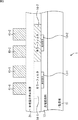
図1に示されるイメージセンサ1は、n型基板11、受光素子(PD:Photo Diode)13−1および13−2を有する光電変換部12、カラーフィルタ14−1および14−2、並びに構造体15−1および15−2などで構成されている。
An
イメージセンサ1においては、光電変換部12の受光素子13−1および13−2上に、波長選択性を有する、カラーフィルタ14−1および14−2がそれぞれ形成されている。さらに、カラーフィルタ14−1および14−2の上部には、中央部分に凹部(窪み)16−1および16−2がそれぞれ形成された平凸形状(レンズ形状)の構造体15−1および15−2がそれぞれ形成されている。また、構造体15−1および15−2の凹部16−1および16−2を除く最上部表面には、光反射性の薄膜17−1および17−2がそれぞれ形成されている。そして、構造体15−1および15−2の凹部16−1および16−2には、図中丸で示されるように、測定対象のゲル状、または液体状の試料21−1および21−2がそれぞれ貯留されている。この丸は、試料が貯留されていることを概念的に示すものである。
In the
なお、以下、特に区別する必要のない場合、受光素子13−1および13−2、カラーフィルタ14−1および14−2、並びに、構造体15−1および15−2は、それぞれ、受光素子13、カラーフィルタ14、並びに構造体15と称する。凹部16−1および16−2、薄膜17−1および17−2、並びに、試料21−1および21−2も、特に区別する必要のない場合、それぞれ、凹部16、薄膜17、並びに、試料21と称する。
In the following description, the light receiving elements 13-1 and 13-2, the color filters 14-1 and 14-2, and the structures 15-1 and 15-2 are respectively the light receiving elements 13 unless otherwise required to be distinguished. ,
また、図1の例においては、受光素子13−1および13−2が2個しか示されていないが、実際には、n型基板11上には、複数の受光素子13がマトリクス状に配設された光電変換部12が構成されている。
In the example of FIG. 1, only two light receiving elements 13-1 and 13-2 are shown, but actually, a plurality of light receiving elements 13 are arranged in a matrix on the n-
n型基板11は、半導体ウェハなどで構成される。光電変換部12は、例えば、CCD(Charge Coupled Device:電荷結合素子)やCMOS(Complementary Metal Oxide Semiconductor:相補性金属酸化膜半導体)などの固体撮像素子により構成される。光電変換部12は、試料21の光現象を検出し、電気信号として出力する。
The n-
カラーフィルタ14は、受光素子13を覆うように、その上部に形成され、特定の波長領域を通過させ、かつ、他の波長領域を吸収、あるいは反射する材料や構造により、波長選択性を有するように形成される。例えば、波長選択性を持たせる方法としては、通常のCCDやCMOSイメージセンサと同様に、一定厚みを有する高分子材料を付加する方法や、無機材料の多層膜を形成して干渉フィルタを構成させる方法などがある。
The
図1の例のカラーフィルタ14−2のハッチは、カラーフィルタ14−1と異なる波長選択性を有していることを示している。このように、カラーフィルタ14は、用途に応じて、画素(受光素子13)毎に異なる波長選択性を持たせる場合もあるが、これに限定されず、例えば、同一の波長選択性を有するフィルタを均一に構成するようにしてもよい。
The hatch of the color filter 14-2 in the example of FIG. 1 indicates that it has a wavelength selectivity different from that of the color filter 14-1. As described above, the
なお、カラーフィルタ14は、試料21に対して光現象を発生させるための励起光の波長が受光素子13や光電変換部12に到達するのを防ぐために設けられる。したがって、例えば、構造体15が波長選択性を有している場合など、励起光を用いることなく光現象が得られる場合には、カラーフィルタ14を省略することも可能である。
The
中央部分に凹部16が形成された平凸形状の構造体15は、光透過材料によって形成されている。構造体15は、カラーフィルタ14の上部、すなわち、光電変換部12の直上領域の所定の位置に、受光素子13を覆うように形成される。この構造体15は、隣接画素との間を区切り、その凹部16に試料21を貯留して光現象の測定を行うために形成される。凹部16を形成することにより、試料21がゲル状、または液体状であっても流れ出したり、隣と混ざることを抑制することができる。なお、試料21は、ゲル状や液体状以外であってもよい。
The plano-
ここで、光現象は、あらゆる方向で観察されるため、受光素子13と反対方向へ出射された光を検出するためには、光を受光素子13方向へと反射させる構造が必要となる。 Here, since the optical phenomenon is observed in all directions, a structure for reflecting the light in the direction of the light receiving element 13 is required to detect the light emitted in the direction opposite to the light receiving element 13.
そのため、構造体15の凹部16の領域を除く、上部表面には、AL、Au、Pt、Crなどの材料からなる光反射性を有する薄膜17が形成されている。これにより、受光素子13が構造体15で起こる光現象を最大限に取り込み、高感度の信号検出を行うことが可能となる。
Therefore, a thin film 17 having light reflectivity made of a material such as AL, Au, Pt, or Cr is formed on the upper surface excluding the region of the
以上のように、イメージセンサ1は、受光素子13並びに光電変換部12が構造体15と一体化して形成されている。これにより、アライメントの処理が不要となる。また、構造体15は、図2を参照して後述するように、ウエハプロセスによって形成することができるので、位置合わせ精度をサブミクロン以内に抑えることが可能になる。
As described above, the
なお、図1の例においては、カラーフィルタ14を、光電変換部12と構造体15の間に設けるようにしたが、カラーフィルタ14を設けることなしに、構造体15自体を、波長選択性を有する材料によって形成してもよい。例えば、構造体15は、特定の波長領域を通過させ、かつ、他の波長領域を吸収、あるいは反射する材料や構造により、波長選択性を有するように形成することもできる。
In the example of FIG. 1, the
次に、図2のフローチャートを参照して、図1のイメージセンサ1の製造方法を説明する。
Next, a method for manufacturing the
ステップS11において、イメージセンサ1の製造装置(以下、製造装置と称する)は、半導体ウェハであるn型基板11を準備する。ステップS12において、製造装置は、図3に示されるように、n型基板11上に、マトリクス状に複数の受光素子13と、光電変換部12とを形成する。
In step S11, the
ステップS13において、製造装置は、受光素子13および光電変換部12の直上領域に、受光素子13を覆うように、波長選択材料からなるカラーフィルタ14のフィルタ層を形成する。
In step S <b> 13, the manufacturing apparatus forms a filter layer of the
なお、上述したステップS11乃至S13における処理は、特に限定されるものではなく、公知の光電変換素子の製造方法などを適用することも可能である。 In addition, the process in step S11 thru | or S13 mentioned above is not specifically limited, It is also possible to apply the manufacturing method of a well-known photoelectric conversion element, etc.
ステップS14において、フィルタ層の上に、有機高分子材料層31を形成する。この有機高分子材料層31が、のちに構造体15となる。
In step S14, the organic
ステップS15において、製造装置は、図3に示されるように、有機高分子材料層31において、カラーフィルタ14の中央部以外を遮光する、すなわち、中央部を露光するレジストパターン41を形成する。レジストパターン41は、受光素子13を覆うように凹部16を有する構造体15が形成されるよう、光電変換部12の直上領域の所定の位置に形成される。
In step S15, as shown in FIG. 3, in the organic
具体的には、製造装置は、有機高分子材料層31の上に、1つのカラーフィルタ14−1の中央部以外を遮光するように、感光性レジスト層を形成する。そして、製造装置は、レジスト層の平凸形状の構造体となる部分以外の領域を露光してレジスト樹脂を硬化させる。現像処理を施すと、硬化された領域以外は除去されて、露光マスクを反転させた領域が、レジストパターン41−1として転写形成される。同様に、1つのカラーフィルタ14−2についても、カラーフィルタ14−2の中央部以外を遮光するレジストパターン41−2が形成される。
Specifically, the manufacturing apparatus forms a photosensitive resist layer on the organic
なお、以下、レジストパターン41−1および41−2を個々に区別する必要がない場合、レジストパターン41と称する。
Hereinafter, the resist patterns 41-1 and 41-2 will be referred to as resist
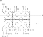
図4は、レジストパターン41が形成されたイメージセンサ1を上から見た上面図である。図4の例のAにおける断面図が、図3に相当する。なお、図4の例においては、カラーフィルタ14が有機高分子材料層31の下層にあるため、カラーフィルタ14を点線で表している。
FIG. 4 is a top view of the
レジストパターン41−1は、カラーフィルタ14−1の中央部以外を遮光するように形成されている。レジストパターン41−2は、カラーフィルタ14−2の中央部以外を遮光するように形成されている。レジストパターン41−3は、カラーフィルタ14−3の中央部以外を遮光するように形成されている。レジストパターン41−(n−1)は、カラーフィルタ14−(n−1)の中央部以外を遮光するように形成されている。レジストパターン41−nは、カラーフィルタ14−nの中央部以外を遮光するように形成されている。レジストパターン41−(n+1)は、カラーフィルタ14−(n+1)の中央部以外を遮光するように形成されている。 The resist pattern 41-1 is formed so as to shield light other than the central portion of the color filter 14-1. The resist pattern 41-2 is formed so as to shield light other than the central portion of the color filter 14-2. The resist pattern 41-3 is formed so as to shield light other than the central portion of the color filter 14-3. The resist pattern 41- (n-1) is formed so as to shield light other than the central portion of the color filter 14- (n-1). The resist pattern 41-n is formed so as to shield light other than the central portion of the color filter 14-n. The resist pattern 41- (n + 1) is formed so as to shield light except for the central portion of the color filter 14- (n + 1).
なお、図4の例においては、カラーフィルタ14およびレジストパターン41が6個しか示されていないが、実際には、複数で構成される。
In the example of FIG. 4, only six
また、図3および図4の例においては、レジストパターン41が中央部を正方形とするように形成されているが、その形は限定されない。また、図3および図4の例においては、レジストパターン41が、カラーフィルタ14の中央部だけでなく、カラーフィルタ14間の境界も除いて形成されているが、これは、次の工程において、有機高分子材料層31があふれてしまうのを防ぐためである。
In the example of FIGS. 3 and 4, the resist
図2に戻って、ステップS16において、製造装置は、レジストパターン41をリフローする。具体的には、製造装置は、レジストパターン41に対して、カラーフィルタ14を熱退色させない範囲の温度を与えることによって、リフロープロセスを行う。リフロープロセスとしては、例えば、特許第3355874号に記載されるオンチップレンズ形成法と同様に、混同ガスを用いたドライエッチングプロセスを施し、有機高分子材料層31を全てエッチバックする方法を用いることができる。
Returning to FIG. 2, in step S <b> 16, the manufacturing apparatus reflows the resist
図5および図6は、構造体15を形成する方法との比較のための、従来のオンチップレンズ形成方法を説明する図である。
5 and 6 are diagrams for explaining a conventional on-chip lens forming method for comparison with the method of forming the
図5に示されるように、従来のオンチップレンズ形成方法において、有機高分子材料層31の上に形成されるレジストパターン51−1は、カラーフィルタ14−1より少し小さめにカラーフィルタ14−1上に形成されていた。同様に、レジストパターン51−2は、カラーフィルタ14−2より少し小さめにカラーフィルタ14−2上に形成されていた。
As shown in FIG. 5, in the conventional on-chip lens forming method, the resist pattern 51-1 formed on the organic
したがって、上述した混同ガスを用いたドライエッチングプロセスを施し、有機高分子材料層31を全てエッチバックする方法により、図6に示されるように、集光に適した平凸形状の、完成度の高いオンチップレンズ61−1および61−2が形成された。
Therefore, by performing a dry etching process using the above-described mixed gas and etching back all the organic
これに対して、イメージセンサ1において、レジストパターン41は、カラーフィルタ14の中央部以外を遮光するように、すなわち、中央部を露光するように形成されている。
On the other hand, in the
したがって、このリフロープロセスにより、図7に示されるように、カラーフィルタ14上に、すなわち、光電変換部12の直上領域の所定の位置に、受光素子13を覆うように、凹部16を有する平凸形状の構造体15が形成される。図7の例においては、カラーフィルタ14−1上には、凹部16−1を有する平凸形状の構造体15−1が形成され、カラーフィルタ14−2上には、凹部16−2を有する平凸形状の構造体15−2が形成される。
Therefore, by this reflow process, as shown in FIG. 7, the plano-convex having the
このように、リフロープロセスを行うことにより、より集光率の高い曲率を持った形状である、平凸形状の構造体15が形成される。
Thus, by performing the reflow process, the plano-
図8は、凹部16を有する平凸形状の構造体15が形成されたイメージセンサ1を上から見た上面図である。図8の例のAにおける断面図が、図7に相当する。
FIG. 8 is a top view of the
凹部16−1を有する平凸形状の構造体15−1は、カラーフィルタ14−1上に形成されている。凹部16−2を有する平凸形状の構造体15−2は、カラーフィルタ14−2上に形成されている。凹部16−3を有する平凸形状の構造体15−3は、カラーフィルタ14−3上に形成されている。凹部16−(n−1)を有する平凸形状の構造体15−(n−1)は、カラーフィルタ14−(n−1)上に形成されている。凹部16−nを有する平凸形状の構造体15−nは、カラーフィルタ14−n上に形成されている。凹部16−(n+1)を有する平凸形状の構造体15−(n+1)は、カラーフィルタ14−(n+1)上に形成されている。 The plano-convex structure 15-1 having the recess 16-1 is formed on the color filter 14-1. A plano-convex structure 15-2 having a recess 16-2 is formed on the color filter 14-2. A plano-convex structure 15-3 having a recess 16-3 is formed on the color filter 14-3. The plano-convex structure 15- (n-1) having the recess 16- (n-1) is formed on the color filter 14- (n-1). A plano-convex structure 15-n having a recess 16-n is formed on the color filter 14-n. The plano-convex structure 15- (n + 1) having the recess 16- (n + 1) is formed on the color filter 14- (n + 1).
なお、図8の例においては、カラーフィルタ14および構造体15が6個しか示されていないが、実際には、複数で構成される。
In the example of FIG. 8, only six
また、図7および図8の例においては、構造体15が模式的に示されているため、構造体15は、カラーフィルタ14の四隅を覆っていないが、実際には、有機高分子材料層31のリフローにより覆うように形成される。
Further, in the examples of FIGS. 7 and 8, since the
さらに、図8の例においては、凹部16が正円で示されているが、凹部16の形状は、楕円でもよいし、円に限らない。すなわち、凹部16の形状は問わない。
Furthermore, in the example of FIG. 8, the
図2に戻って、ステップS17において、製造装置は、構造体15の上表面のうち、中央の凹部16を除いた領域に光反射材料を付加する。
Returning to FIG. 2, in step S <b> 17, the manufacturing apparatus adds a light reflecting material to a region of the upper surface of the
製造装置は、構造体15の上表面のうち、中央の凹部16を除いた領域に対して、蒸着や塗布などのプロセスで光反射性材料を付加し、光反射性の薄膜17を形成する。光反射材料としては、例えば、AL、Au、Pt、またはCrなどの金属材料が用いられる。
The manufacturing apparatus adds a light reflective material to the region of the upper surface of the
これにより、構造体15で起こる光現象のうち、上部方向へ散逸する光を、受光素子13側に反射させて、イメージセンサ1に取り込み、高感度の信号検出を行うことができるようになる。
As a result, of the light phenomenon occurring in the
再度、図2に戻り、ステップS18において、製造装置は、構造体15の形成されたウェハを切断してチップ化する。
Returning to FIG. 2 again, in step S18, the manufacturing apparatus cuts the wafer on which the
以上のように、半導体チップなどの製造技術を応用して、イメージセンサ1が製造されるので、光電変換部12の直上域の所定の位置(すなわち、受光素子13を覆う位置)に、精度よく平凸形状の構造体15を形成することができる。
As described above, since the
また、受光素子13と光電変換部12と凹部16を有する構造体15とが一体で形成されるので、アライメントの手段が不要になる。これにより、装置を小型化および簡素化することができるので、低コストを実現することができる。
In addition, since the light receiving element 13, the
[撮像素子の構成例]
図9は、本開示を適用した撮像素子としてのイメージセンサの他の実施の形態の構成を模式的に示す断面図である。
[Configuration example of image sensor]
FIG. 9 is a cross-sectional view schematically showing a configuration of another embodiment of an image sensor as an imaging device to which the present disclosure is applied.
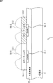
図9に示されるイメージセンサ71は、n型基板11、受光素子81−1乃至84−1、および受光素子81−2乃至84−2を有する光電変換部12、カラーフィルタ14−1および14−2、並びに構造体15−1および15−2などで構成されている。
An
なお、図9は、断面図であるので、受光素子83−1および84−1、並びに、受光素子83−2および84−2の図示はされていないが、図9の例の場合、実際には、4つの受光素子に対して単一の構造体が形成されている。 Since FIG. 9 is a cross-sectional view, the light receiving elements 83-1 and 84-1 and the light receiving elements 83-2 and 84-2 are not shown, but in the case of the example of FIG. A single structure is formed for the four light receiving elements.
すなわち、図1のイメージセンサ1は、1つの受光素子に対して単一の構造体が形成されていた。これに対して、イメージセンサ71においては、複数の受光素子81−1乃至84−1上に、波長選択性を有するカラーフィルタ14−1が形成され、複数の画素に対して単一の構造体15−1が形成されている。また、複数の受光素子81−2乃至84−2上に、波長選択性を有するカラーフィルタ14−2が形成され、複数の画素に対して単一の構造体15−2が形成されている。
That is, in the
そして、図1のイメージセンサ1と同様に、カラーフィルタ14−1および14−2の上部には、中央部分に凹部(窪み)16−1および16−2がそれぞれ形成された平凸形状の構造体15−1および15−2がそれぞれ形成されている。また、構造体15−1および15−2の凹部16−1および16−2を除く最上部表面には、光反射性の薄膜17−1および17−2がそれぞれ形成されている。そして、構造体15−1および15−2の凹部16−1および16−2には、図中丸で示されるように、測定対象のゲル状、または液体状の試料21−1および21−2がそれぞれ貯留されている。
As in the
なお、以下、受光素子81−1乃至84−1、および受光素子81−2乃至84−2を個々に区別しない場合、受光素子81乃至84と称する。 Hereinafter, the light receiving elements 81-1 to 84-1 and the light receiving elements 81-2 to 84-2 will be referred to as the light receiving elements 81 to 84 unless they are individually distinguished.
また、図9の例においては、受光素子81乃至84に対して、単一の構造体15が形成される例を説明したが、受光素子の数は4つに限らず、6つやもっと多く構成するようにしてもよい。
In the example of FIG. 9, the example in which the
このように、1つの試料21−1に対して複数の画素(受光素子81−1乃至84−1)を設置して光現象を検出することで、信号S/N比を高めることが可能になる。また、隣接する試料21−2に対しても、同様に、対応する複数の画素(受光素子81−2乃至84−2)およびカラーフィルタ14−2により光現象が検出される。これにより、画素数が同一の場合には、検出密度が低下するものの、図1のイメージセンサ1と比して、高感度での信号検出が可能になる。
As described above, the signal S / N ratio can be increased by installing a plurality of pixels (light receiving elements 81-1 to 84-1) for one sample 21-1 and detecting a light phenomenon. Become. Similarly, for the adjacent sample 21-2, the light phenomenon is detected by the corresponding pixels (light receiving elements 81-2 to 84-2) and the color filter 14-2. As a result, when the number of pixels is the same, the detection density is lowered, but the signal can be detected with higher sensitivity than the
また、イメージセンサ71も、受光素子81乃至84および光電変換部12が、凹部16を有する構造体15と一体で形成されているため、アライメント作業や手段が不要となる。さらに、イメージセンサ71も、その図示と説明は省略するが、図2を参照して上述したイメージセンサ1の製造方法と同様に製造することが可能であるので、位置合わせ精度をサブミクロン以内に抑えることができる。
Further, since the light receiving elements 81 to 84 and the
以上のように、本開示によれば、受光素子および光電変換部と、凹部を有する構造体とを一体化して形成しているので、装置を小型化、および簡素化することができるとともに、低コストで製造することができる。 As described above, according to the present disclosure, since the light receiving element, the photoelectric conversion unit, and the structure having the recess are integrally formed, the apparatus can be downsized and simplified, and the low Can be manufactured at cost.
また、本開示によれば、受光素子上に設けられた平凸形状の構造体の、凹部以外の最表面に光反射性の薄膜が付加されているので、試料から上部方向(受光素子と反対方向)に出射された光現象を反射し、受光素子側に導くことができる。これにより、信号の検出感度を高めることができる。 In addition, according to the present disclosure, a light-reflective thin film is added to the outermost surface of the plano-convex structure provided on the light receiving element other than the recessed part, so that the sample is directed upward (opposite to the light receiving element). The light phenomenon emitted in the direction) can be reflected and guided to the light receiving element side. Thereby, the detection sensitivity of a signal can be improved.
このように信号の検出感度を高めることにより、検出誤差を小さくし、かつ、少ない試料から確実に化学反応を検出することが可能になる。 By increasing the signal detection sensitivity in this way, it is possible to reduce detection errors and reliably detect chemical reactions from a small number of samples.
<2.第2の実施の形態>
[検査装置の構成例]
図10は、本開示を適用した撮像素子としてのイメージセンサを用いた検査装置の一実施の形態の構成を模式的に示す図である。
<2. Second Embodiment>
[Configuration example of inspection equipment]
Figure 10 is a diagram schematically showing a configuration of an embodiment of an inspection apparatus using an image sensor as an imaging element of the present disclosure.
図10に示される検査装置100は、撮像装置101、光源102、および試料注入部103により構成される。撮像装置101は、図1のイメージセンサ1、制御部111、画像処理部112、メモリ113、表示部114、および送信部115により構成される。
The
イメージセンサ1の受光素子13および光電変換部12は、制御部111の制御のもと、凹部16に試料が貯留された状態の構造体15で起こる光現象を取り込み、電気信号として、画像処理部112に出力する。
Under the control of the control unit 111, the light receiving element 13 and the
制御部111は、撮像装置101の各部を制御するとともに、光源102の発光タイミングを制御し、試料注入部103の試料の注入タイミングを制御する。例えば、制御部111は、イメージセンサ1の撮像タイミングを制御したり、画像処理部112の画像処理を制御したり、送信部115の送信を制御する。
The control unit 111 controls each unit of the
画像処理部112は、制御部111の制御のもと、イメージセンサ1からの電気信号に対応する画像に適した信号処理を行い、処理後の画像やデータを、メモリ113に記録したり、表示部114に表示させる。例えば、画像処理部112は、イメージセンサ1からの電気信号に対応する画像を処理して、配列のデータや反応しているかしていないかのデータを出力する。
The
メモリ113は、画像処理部112により処理された画像やデータを記憶する。表示部114は、画像処理部112により処理された画像やデータを表示する。送信部115は、メモリ113に蓄積された画像やデータを、例えば、USBケーブルなどで接続される装置(図示せぬ)に送信する。
The
光源102は、制御部111からのタイミングで発光する。試料注入部103は、制御部111からの制御に応じて、イメージセンサ1の構造体15が有する凹部16に、検査対象の試料を注入する。
The
以上のように、図10の検査装置100においては、受光素子13並びに光電変換部12が構造体15と一体化して形成されているイメージセンサ1を用いることによって、アライメントの処理や手段が不要となる。この結果、装置の小規模、低コスト化を実現することができる。
As described above, in the
また、位置合わせ精度をサブミクロン以内に抑えることが可能になり、精度のよい検査を行うことができる。 In addition, the alignment accuracy can be suppressed to within submicrons, and a high-precision inspection can be performed.
なお、本開示の実施の形態は、上述した実施の形態に限定されるものではなく、本開示の要旨を逸脱しない範囲において種々の変更が可能である。 The embodiment of the present disclosure is not limited to the above-described embodiment, and various modifications can be made without departing from the gist of the present disclosure.
以上、添付図面を参照しながら本開示の好適な実施形態について詳細に説明したが、本開示はかかる例に限定されない。本開示の属する技術の分野における通常の知識を有する者であれば、特許請求の範囲に記載された技術的思想の範疇内において、各種の変更例または修正例に想到し得ることは明らかであり、これらについても、当然に本開示の技術的範囲に属するものと了解される。 The preferred embodiments of the present disclosure have been described in detail above with reference to the accompanying drawings, but the present disclosure is not limited to such examples. It is obvious that a person having ordinary knowledge in the technical field to which the present disclosure belongs can come up with various changes or modifications within the scope of the technical idea described in the claims. Of course, it is understood that these also belong to the technical scope of the present disclosure.
なお、本技術は以下のような構成も取ることができる。
(1) 複数の受光素子と、
前記受光素子に入射した光を電気信号に変換する光電変換部と、
前記受光素子を覆うように形成された平凸形状の構造体と
を備え、
前記構造体は、前記平凸形状の中央部分に凹部を有し、
前記構造体の表面のうち、前記凹部を除いた領域は、光反射材料によって覆われている
撮像素子。
(2) 前記構造体は、光透過材料により形成されている
前記(1)に記載の撮像素子。
(3) 前記構造体と前記光電変換部との間に、特定波長領域を吸収する、あるいは、特定波長領域を透過する光機能性材料により形成される層
をさらに備える前記(1)または(2)に記載の撮像素子。
(4) 前記構造体は、特定波長領域を吸収する、あるいは、特定波長領域を透過する光機能性材料により形成される
前記(1)に記載の撮像素子。
(5) 前記構造体は、前記受光素子の単一画素、または複数画素毎に形成されている
前記(1)乃至(4)のいずれかに記載の撮像素子。
(6) 複数の受光素子と、
前記受光素子に入射した光を電気信号に変換する光電変換部と、
前記受光素子を覆うように形成された平凸形状の構造体とからなり、
前記構造体は、前記平凸形状の中央部分に凹部を有し、前記構造体の表面のうち、前記凹部を除いた領域は、光反射材料によって覆われている撮像素子
を備える電子機器。
(7) 受光素子および光電変換部が形成されたウェハ上に、有機高分子材料層を形成し、
前記有機高分子材料層上における前記光電変換部の直上領域の所定の位置に、その中央部分以外を遮光するレジストパターンを形成し、
前記レジストパターンをリフローすることにより、前記受光素子を覆うように形成され、前記中央部分に凹部を有する平凸形状の構造体を生成し、
前記構造体の表面のうち、前記凹部を除いた領域に光反射材料を付加する
撮像素子の製造方法。
(8) 複数の受光素子と、前記受光素子に入射した光を電気信号に変換する光電変換部と、前記受光素子を覆うように形成された平凸形状の構造体とからなり、前記構造体は、前記平凸形状の中央部分に凹部を有し、前記構造体の表面のうち、前記凹部を除いた領域は、光反射材料によって覆われている撮像素子と、
前記凹部に充填された試料に対して光を照射する光源と、
前記光源と前記撮像素子とを制御する制御部と
を備える検査装置。
In addition, this technique can also take the following structures.
(1) a plurality of light receiving elements;
A photoelectric conversion unit that converts light incident on the light receiving element into an electrical signal;
A plano-convex structure formed so as to cover the light receiving element,
The structure has a recess in a center portion of the plano-convex shape,
The area | region except the said recessed part among the surfaces of the said structure is covered with the light reflection material.
(2) The imaging device according to (1), wherein the structure is made of a light transmitting material.
(3) The (1) or (2) further comprising a layer formed of an optical functional material that absorbs a specific wavelength region or transmits a specific wavelength region between the structure and the photoelectric conversion unit. ).
(4) The imaging device according to (1), wherein the structure is formed of an optical functional material that absorbs a specific wavelength region or transmits a specific wavelength region.
(5) The imaging device according to any one of (1) to (4), wherein the structure is formed for each single pixel or a plurality of pixels of the light receiving element.
(6) a plurality of light receiving elements;
A photoelectric conversion unit that converts light incident on the light receiving element into an electrical signal;
A plano-convex structure formed so as to cover the light receiving element,
An electronic apparatus comprising: an imaging element in which the structure has a recess in a center portion of the plano-convex shape, and a region of the surface of the structure excluding the recess is covered with a light reflecting material.
(7) An organic polymer material layer is formed on the wafer on which the light receiving element and the photoelectric conversion unit are formed,
On the organic polymer material layer, a resist pattern that shields light other than the central portion is formed at a predetermined position in the region immediately above the photoelectric conversion unit,
By reflowing the resist pattern, it is formed so as to cover the light receiving element, and a plano-convex structure having a concave portion in the central portion is generated,
A method for manufacturing an imaging element, wherein a light reflecting material is added to a region of the surface of the structure body excluding the concave portion.
(8) The structure includes a plurality of light receiving elements, a photoelectric conversion unit that converts light incident on the light receiving elements into an electric signal, and a plano-convex structure formed so as to cover the light receiving elements. Has a concave portion in the center portion of the plano-convex shape, and an image sensor in which the region excluding the concave portion of the surface of the structure is covered with a light reflecting material;
A light source for irradiating light to the sample filled in the recess;
An inspection apparatus comprising: a control unit that controls the light source and the imaging device.
1 イメージセンサ, 11 n型基板, 12 光電変換部, 13−1,13−2,13 受光素子, 14−1,14−2,14 カラーフィルタ, 15−1,15−2,15 構造体, 16−1,16−2,16 凹部, 17−1,17−2,17 薄膜, 21−1,21−2,21 試料, 71 イメージセンサ, 81−1乃至84−1,81−2乃至84−2, 81乃至84 受光素子, 100 検査装置, 101 撮像装置, 111 制御部, 112 画像処理部, 113 メモリ, 114 表示部, 115 送信部
DESCRIPTION OF
Claims (7)
前記受光素子に入射した光を電気信号に変換する光電変換部と、
前記受光素子を覆うように形成された平凸レンズ形状の構造体と
を備え、
前記構造体は、前記平凸レンズ形状の中央部分に、検査対象の試料を注入するための凹部を有し、
前記構造体の表面のうち、前記凹部を除いた領域は、光反射材料によって覆われており、
前記構造体は、前記受光素子の単一画素、または複数画素毎に形成されている
撮像素子。 A plurality of light receiving elements;
A photoelectric conversion unit that converts light incident on the light receiving element into an electrical signal;
And a structure of a plano-convex lens shape formed so as to cover the light receiving element,
Wherein the structure, the central portion of the plano-convex lens shape has a recess for injecting a sample to be inspected,
Of the surface of the structure, the region excluding the recess is covered with a light reflecting material ,
The said structure is an image pick-up element currently formed for every single pixel of the said light receiving element, or several pixels .
請求項1に記載の撮像素子。 The imaging device according to claim 1, wherein the structure is made of a light transmissive material.
をさらに備える請求項2に記載の撮像素子。 The imaging device according to claim 2, further comprising: a layer formed of an optical functional material that absorbs a specific wavelength region or transmits a specific wavelength region between the structure and the photoelectric conversion unit.
請求項1に記載の撮像素子。 The imaging device according to claim 1, wherein the structure is formed of an optical functional material that absorbs a specific wavelength region or transmits a specific wavelength region.
前記受光素子に入射した光を電気信号に変換する光電変換部と、
前記受光素子を覆うように形成された平凸レンズ形状の構造体とからなり、
前記構造体は、前記平凸レンズ形状の中央部分に、検査対象の試料を注入するための凹部を有し、前記構造体の表面のうち、前記凹部を除いた領域は、光反射材料によって覆われており、
前記構造体は、前記受光素子の単一画素、または複数画素毎に形成されている
撮像素子
を備える電子機器。 A plurality of light receiving elements;
A photoelectric conversion unit that converts light incident on the light receiving element into an electrical signal;
Consists of a structure of a plano-convex lens shape formed so as to cover the light receiving element,
Wherein the structure, the central portion of the plano-convex lens shape has a recess for injecting a sample to be tested, of the surface of the structure, regions other than the recess, covered by the light reflecting material We are,
The electronic device including the imaging element, wherein the structure is formed for each single pixel or a plurality of pixels of the light receiving element .
前記有機高分子材料層上における前記光電変換部の直上領域の所定の位置に、その中央部以外を遮光するレジスト層を形成し、
前記レジスト層の平凸レンズ形状の構造体となる部分以外の領域を露光して、レジスト樹脂を硬化させて、現像処理により硬化された領域以外を除去、露光マスクを反転させた領域を、レジストパターンとして形成し、
前記レジストパターンをリフローすることにより、前記受光素子を覆うように形成され、前記中央部分に、検査対象の試料を注入するための凹部を有する前記平凸レンズ形状の構造体を生成し、
前記構造体の表面のうち、前記凹部を除いた領域に光反射材料を付加する
撮像素子の製造方法。 An organic polymer material layer is formed on the wafer on which the light receiving element and the photoelectric conversion unit are formed,
Forming a resist layer that shields light other than the central portion at a predetermined position in the region immediately above the photoelectric conversion portion on the organic polymer material layer,
The resist layer is exposed to a region other than a portion that becomes a plano-convex lens-shaped structure, the resist resin is cured, the region other than the region cured by the development process is removed, and the region where the exposure mask is inverted is a resist pattern. Formed as
Wherein by reflowing the resist pattern is formed so as to cover the light receiving element, the said central portion to generate a structure of the plano-convex lens shape having a concave portion for injecting a sample to be inspected,
A method for manufacturing an imaging element, wherein a light reflecting material is added to a region of the surface of the structure body excluding the concave portion.
撮像素子と、
前記凹部に注入された試料に対して光を照射する光源と、
前記光源と前記撮像素子とを制御する制御部と
を備える検査装置。 Consists of a plurality of light receiving elements, and a photoelectric converter for converting light incident on the light receiving element into an electric signal, and the structure of the plano-convex lens shape formed so as to cover the light receiving element, wherein the structure, having a recess in a central portion of the plano-convex lens shape, of the surface of the structure, regions other than the concave portion is covered by a light reflecting material, the structure, the single light receiving element An image sensor formed for each pixel or each of a plurality of pixels ;
A light source for irradiating light to the sample injected into the recess;
An inspection apparatus comprising: a control unit that controls the light source and the imaging device.
Priority Applications (2)
| Application Number | Priority Date | Filing Date | Title |
|---|---|---|---|
| JP2011137983A JP5765081B2 (en) | 2011-06-22 | 2011-06-22 | Image sensor, electronic device, manufacturing method, and inspection apparatus |
| US13/524,970 US20120326011A1 (en) | 2011-06-22 | 2012-06-15 | Image pickup device, electronic apparatus, manufacturing method, and inspection apparatus |
Applications Claiming Priority (1)
| Application Number | Priority Date | Filing Date | Title |
|---|---|---|---|
| JP2011137983A JP5765081B2 (en) | 2011-06-22 | 2011-06-22 | Image sensor, electronic device, manufacturing method, and inspection apparatus |
Publications (3)
| Publication Number | Publication Date |
|---|---|
| JP2013004938A JP2013004938A (en) | 2013-01-07 |
| JP2013004938A5 JP2013004938A5 (en) | 2014-07-03 |
| JP5765081B2 true JP5765081B2 (en) | 2015-08-19 |
Family
ID=47360945
Family Applications (1)
| Application Number | Title | Priority Date | Filing Date |
|---|---|---|---|
| JP2011137983A Expired - Fee Related JP5765081B2 (en) | 2011-06-22 | 2011-06-22 | Image sensor, electronic device, manufacturing method, and inspection apparatus |
Country Status (2)
| Country | Link |
|---|---|
| US (1) | US20120326011A1 (en) |
| JP (1) | JP5765081B2 (en) |
Families Citing this family (5)
| Publication number | Priority date | Publication date | Assignee | Title |
|---|---|---|---|---|
| JP2015096846A (en) * | 2013-10-10 | 2015-05-21 | シスメックス株式会社 | Test substance detection method, fluorescence detection method, and test substance detector and fluorescence detector used for the detection methods |
| US10044959B2 (en) * | 2015-09-24 | 2018-08-07 | Qualcomm Incorporated | Mask-less phase detection autofocus |
| US11417023B2 (en) * | 2018-10-04 | 2022-08-16 | Sony Corporation | Image processing device, image processing method, and program |
| US10957731B1 (en) * | 2019-10-04 | 2021-03-23 | Visera Technologies Company Limited | Sensor device and method for manufacturing the same |
| US20230104190A1 (en) * | 2021-10-01 | 2023-04-06 | Visera Technologies Company Limited | Image sensor |
Family Cites Families (43)
| Publication number | Priority date | Publication date | Assignee | Title |
|---|---|---|---|---|
| GB8716285D0 (en) * | 1987-07-10 | 1987-08-19 | Medical Res Council | Light collecting device |
| US5018866A (en) * | 1989-09-12 | 1991-05-28 | Packard Instrument Company | Method and apparatus for performing high sensitivity fluorescence measurements |
| US5784507A (en) * | 1991-04-05 | 1998-07-21 | Holm-Kennedy; James W. | Integrated optical wavelength discrimination devices and methods for fabricating same |
| US5159199A (en) * | 1991-08-12 | 1992-10-27 | The United States Of America As Represented By The Administrator Of The National Aeronautics And Space Administration | Integrated filter and detector array for spectral imaging |
| JP3344158B2 (en) * | 1995-05-19 | 2002-11-11 | ソニー株式会社 | Manufacturing method of imaging device |
| US6485690B1 (en) * | 1999-05-27 | 2002-11-26 | Orchid Biosciences, Inc. | Multiple fluid sample processor and system |
| US6656432B1 (en) * | 1999-10-22 | 2003-12-02 | Ngk Insulators, Ltd. | Micropipette and dividedly injectable apparatus |
| AU2001236597A1 (en) * | 2000-01-31 | 2001-08-07 | Board Of Regents, The University Of Texas System | System and method for the analysis of bodily fluids |
| EP2202001A3 (en) * | 2000-02-23 | 2011-05-18 | Zyomyx, Inc. | Microfluidic devices and methods |
| US7998746B2 (en) * | 2000-08-24 | 2011-08-16 | Robert Otillar | Systems and methods for localizing and analyzing samples on a bio-sensor chip |
| JP4534352B2 (en) * | 2000-12-27 | 2010-09-01 | 株式会社ニコン | Organic molecule detecting semiconductor element, organic molecule detecting semiconductor device, and organic molecule measuring method using the same |
| DE10111420A1 (en) * | 2001-03-09 | 2002-09-12 | Gnothis Holding Sa Ecublens | To detect an analyte by fluorescence correlation spectroscopy, a set gap is established between the light focusing unit and the volume of the sample, and the sample carrier is thermally insulated from the light source |
| US6785002B2 (en) * | 2001-03-16 | 2004-08-31 | Optical Coating Laboratory, Inc. | Variable filter-based optical spectrometer |
| US6800849B2 (en) * | 2001-12-19 | 2004-10-05 | Sau Lan Tang Staats | Microfluidic array devices and methods of manufacture and uses thereof |
| FR2846420B1 (en) * | 2002-10-24 | 2006-05-05 | Commissariat Energie Atomique | INTEGRATED LUMINESCENCE READING DEVICE |
| WO2005098379A1 (en) * | 2004-04-08 | 2005-10-20 | Purdue Research Foundation | Multi-spectral detector and analysis system |
| US7291824B2 (en) * | 2005-12-22 | 2007-11-06 | Palo Alto Research Center Incorporated | Photosensing throughout energy range and in subranges |
| US7310153B2 (en) * | 2004-08-23 | 2007-12-18 | Palo Alto Research Center, Incorporated | Using position-sensitive detectors for wavelength determination |
| US7262859B2 (en) * | 2004-10-13 | 2007-08-28 | U.S. Genomics, Inc. | Systems and methods for measurement optimization |
| JP4741855B2 (en) * | 2005-02-18 | 2011-08-10 | カシオ計算機株式会社 | Biopolymer analysis chip, analysis support apparatus, and biopolymer analysis method |
| US7358476B2 (en) * | 2005-12-22 | 2008-04-15 | Palo Alto Research Center Incorporated | Sensing photons from objects in channels |
| US7315667B2 (en) * | 2005-12-22 | 2008-01-01 | Palo Alto Research Center Incorporated | Propagating light to be sensed |
| US8437582B2 (en) * | 2005-12-22 | 2013-05-07 | Palo Alto Research Center Incorporated | Transmitting light with lateral variation |
| EP1882916A1 (en) * | 2006-07-20 | 2008-01-30 | Interuniversitair Microelektronica Centrum | Compact catadioptric spectrometer |
| US8629986B2 (en) * | 2006-08-09 | 2014-01-14 | Biozoom Technologies, Inc. | Optical filter and method for the production of the same, and device for the examination of electromagnetic radiation |
| WO2008063135A1 (en) * | 2006-11-24 | 2008-05-29 | Agency For Science, Technology And Research | Apparatus for processing a sample in a liquid droplet and method of using the same |
| US7718948B2 (en) * | 2006-12-04 | 2010-05-18 | Palo Alto Research Center Incorporated | Monitoring light pulses |
| US7879390B2 (en) * | 2007-05-30 | 2011-02-01 | Palo Alto Research Center Incorporated | Surface energy control methods for color filter printing |
| KR100808114B1 (en) * | 2007-07-18 | 2008-02-29 | (주)실리콘화일 | Diagnosis device and method of manufacturing the diagnosis device |
| JP5433580B2 (en) * | 2007-11-02 | 2014-03-05 | バイオシアス ライフ サイエンシーズ, インコーポレイテッド | Sample injection system |
| US8115920B2 (en) * | 2007-11-14 | 2012-02-14 | 3M Innovative Properties Company | Method of making microarrays |
| US8373860B2 (en) * | 2008-02-01 | 2013-02-12 | Palo Alto Research Center Incorporated | Transmitting/reflecting emanating light with time variation |
| US20090262355A1 (en) * | 2008-03-27 | 2009-10-22 | Plexera, Llc | Surface plasmon resonance system and apparatus for interrogating a microarray |
| KR101065077B1 (en) * | 2008-11-05 | 2011-09-15 | 삼성전자주식회사 | Substrate for detecting samples, Bio-chip employ the same, method of fabricating the substrate for detecting samples, and apparatus for detecting bio-material |
| DK2391451T3 (en) * | 2009-02-02 | 2018-10-15 | Opko Diagnostics Llc | STRUCTURES FOR MANAGING LIGHT INTERACTION WITH MICROFLUIDIC DEVICES |
| US8921280B2 (en) * | 2009-02-11 | 2014-12-30 | Samsung Electronics Co., Ltd. | Integrated bio-chip and method of fabricating the integrated bio-chip |
| JP2011059095A (en) * | 2009-08-12 | 2011-03-24 | Sony Corp | Light detection device |
| JP2011038922A (en) * | 2009-08-12 | 2011-02-24 | Sony Corp | Light detection chip, and light detection device using the same |
| EP2293032A1 (en) * | 2009-09-04 | 2011-03-09 | Radisens Diagnostic Limited | An Integrated Cytometric Sensor System and Method |
| WO2011156713A1 (en) * | 2010-06-11 | 2011-12-15 | Vanderbilt University | Multiplexed interferometric detection system and method |
| US8277659B2 (en) * | 2010-09-23 | 2012-10-02 | Battelle Memorial Institute | Microchip capillary electrophoresis absent electrokinetic injection |
| US9029800B2 (en) * | 2011-08-09 | 2015-05-12 | Palo Alto Research Center Incorporated | Compact analyzer with spatial modulation and multiple intensity modulated excitation sources |
| WO2013159116A1 (en) * | 2012-04-20 | 2013-10-24 | University Of Chicago | Fluidic devices for biospecimen preservation |
-
2011
- 2011-06-22 JP JP2011137983A patent/JP5765081B2/en not_active Expired - Fee Related
-
2012
- 2012-06-15 US US13/524,970 patent/US20120326011A1/en not_active Abandoned
Also Published As
| Publication number | Publication date |
|---|---|
| JP2013004938A (en) | 2013-01-07 |
| US20120326011A1 (en) | 2012-12-27 |
Similar Documents
| Publication | Publication Date | Title |
|---|---|---|
| CN102110704B (en) | The method of imageing sensor, shop drawings image-position sensor and sensor device | |
| JP5195112B2 (en) | Refractive index sensor, refractive index sensor array and biosensor | |
| JP5765081B2 (en) | Image sensor, electronic device, manufacturing method, and inspection apparatus | |
| JP6850332B2 (en) | Imaging system | |
| EP1325776B1 (en) | Semiconductor device for detecting organic molecules and method for measuring organic molecules using the same | |
| KR102023216B1 (en) | Chemical sensor, chemical sensor module, biomolecule detection device and biomolecule detection method | |
| TWI521205B (en) | Chemical detectors, biological molecular detection devices and biological molecular detection methods | |
| JP3579321B2 (en) | Two-dimensional imaging surface plasmon resonance measurement apparatus and measurement method | |
| CN103733341B (en) | Imaging sensor, its manufacture method and check device | |
| TW201239344A (en) | Substrate inspection apparatus and substrate inspection method | |
| CN101680839A (en) | biochip | |
| KR20180058005A (en) | Optical inspection apparatus and method, and method for fabricating semiconductor using the inspection apparatus | |
| JP2013004938A5 (en) | ||
| KR101030303B1 (en) | Method of Testing Array Type Light Source using Image Sensor | |
| JP2003215035A (en) | Refractive index measuring device | |
| JP5991370B2 (en) | Chemical sensor, chemical sensor manufacturing method, chemical substance detection apparatus | |
| JP2004260250A (en) | Image pickup element | |
| JP5274031B2 (en) | Analysis method and analyzer | |
| TW202331227A (en) | Biomolecular image sensor and method thereof for detecting biological molecules | |
| JP6270277B2 (en) | Image sensor, inspection apparatus, and inspection method | |
| KR20070002322A (en) | Apparatus and method for gaining a patterned image | |
| JPS6067845A (en) | Foreign matter inspecting device | |
| JP2009264746A (en) | Defect detection device | |
| JP2008304327A (en) | Light detecting device and specimen imaging method | |
| JP2004053258A (en) | Foreign substance inspection apparatus and method |
Legal Events
| Date | Code | Title | Description |
|---|---|---|---|
| A521 | Request for written amendment filed |
Free format text: JAPANESE INTERMEDIATE CODE: A523 Effective date: 20140516 |
|
| A621 | Written request for application examination |
Free format text: JAPANESE INTERMEDIATE CODE: A621 Effective date: 20140516 |
|
| A977 | Report on retrieval |
Free format text: JAPANESE INTERMEDIATE CODE: A971007 Effective date: 20150227 |
|
| A131 | Notification of reasons for refusal |
Free format text: JAPANESE INTERMEDIATE CODE: A131 Effective date: 20150303 |
|
| A521 | Request for written amendment filed |
Free format text: JAPANESE INTERMEDIATE CODE: A523 Effective date: 20150427 |
|
| TRDD | Decision of grant or rejection written | ||
| A01 | Written decision to grant a patent or to grant a registration (utility model) |
Free format text: JAPANESE INTERMEDIATE CODE: A01 Effective date: 20150519 |
|
| A61 | First payment of annual fees (during grant procedure) |
Free format text: JAPANESE INTERMEDIATE CODE: A61 Effective date: 20150601 |
|
| R151 | Written notification of patent or utility model registration |
Ref document number: 5765081 Country of ref document: JP Free format text: JAPANESE INTERMEDIATE CODE: R151 |
|
| R250 | Receipt of annual fees |
Free format text: JAPANESE INTERMEDIATE CODE: R250 |
|
| R250 | Receipt of annual fees |
Free format text: JAPANESE INTERMEDIATE CODE: R250 |
|
| R250 | Receipt of annual fees |
Free format text: JAPANESE INTERMEDIATE CODE: R250 |
|
| LAPS | Cancellation because of no payment of annual fees |