JP5756594B2 - Image processing apparatus and image processing method - Google Patents
Image processing apparatus and image processing method Download PDFInfo
- Publication number
- JP5756594B2 JP5756594B2 JP2009264631A JP2009264631A JP5756594B2 JP 5756594 B2 JP5756594 B2 JP 5756594B2 JP 2009264631 A JP2009264631 A JP 2009264631A JP 2009264631 A JP2009264631 A JP 2009264631A JP 5756594 B2 JP5756594 B2 JP 5756594B2
- Authority
- JP
- Japan
- Prior art keywords
- image
- image processing
- pixel data
- data
- processing unit
- Prior art date
- Legal status (The legal status is an assumption and is not a legal conclusion. Google has not performed a legal analysis and makes no representation as to the accuracy of the status listed.)
- Expired - Fee Related
Links
Images


Classifications
-
- G—PHYSICS
- G06—COMPUTING; CALCULATING OR COUNTING
- G06F—ELECTRIC DIGITAL DATA PROCESSING
- G06F3/00—Input arrangements for transferring data to be processed into a form capable of being handled by the computer; Output arrangements for transferring data from processing unit to output unit, e.g. interface arrangements
- G06F3/14—Digital output to display device ; Cooperation and interconnection of the display device with other functional units
- G06F3/1423—Digital output to display device ; Cooperation and interconnection of the display device with other functional units controlling a plurality of local displays, e.g. CRT and flat panel display
- G06F3/1446—Digital output to display device ; Cooperation and interconnection of the display device with other functional units controlling a plurality of local displays, e.g. CRT and flat panel display display composed of modules, e.g. video walls
-
- G—PHYSICS
- G09—EDUCATION; CRYPTOGRAPHY; DISPLAY; ADVERTISING; SEALS
- G09G—ARRANGEMENTS OR CIRCUITS FOR CONTROL OF INDICATING DEVICES USING STATIC MEANS TO PRESENT VARIABLE INFORMATION
- G09G2310/00—Command of the display device
- G09G2310/02—Addressing, scanning or driving the display screen or processing steps related thereto
- G09G2310/0232—Special driving of display border areas
-
- G—PHYSICS
- G09—EDUCATION; CRYPTOGRAPHY; DISPLAY; ADVERTISING; SEALS
- G09G—ARRANGEMENTS OR CIRCUITS FOR CONTROL OF INDICATING DEVICES USING STATIC MEANS TO PRESENT VARIABLE INFORMATION
- G09G2340/00—Aspects of display data processing
- G09G2340/04—Changes in size, position or resolution of an image
- G09G2340/0407—Resolution change, inclusive of the use of different resolutions for different screen areas
-
- G—PHYSICS
- G09—EDUCATION; CRYPTOGRAPHY; DISPLAY; ADVERTISING; SEALS
- G09G—ARRANGEMENTS OR CIRCUITS FOR CONTROL OF INDICATING DEVICES USING STATIC MEANS TO PRESENT VARIABLE INFORMATION
- G09G2340/00—Aspects of display data processing
- G09G2340/10—Mixing of images, i.e. displayed pixel being the result of an operation, e.g. adding, on the corresponding input pixels
-
- G—PHYSICS
- G09—EDUCATION; CRYPTOGRAPHY; DISPLAY; ADVERTISING; SEALS
- G09G—ARRANGEMENTS OR CIRCUITS FOR CONTROL OF INDICATING DEVICES USING STATIC MEANS TO PRESENT VARIABLE INFORMATION
- G09G2360/00—Aspects of the architecture of display systems
- G09G2360/06—Use of more than one graphics processor to process data before displaying to one or more screens
-
- G—PHYSICS
- G09—EDUCATION; CRYPTOGRAPHY; DISPLAY; ADVERTISING; SEALS
- G09G—ARRANGEMENTS OR CIRCUITS FOR CONTROL OF INDICATING DEVICES USING STATIC MEANS TO PRESENT VARIABLE INFORMATION
- G09G2360/00—Aspects of the architecture of display systems
- G09G2360/08—Power processing, i.e. workload management for processors involved in display operations, such as CPUs or GPUs
-
- G—PHYSICS
- G09—EDUCATION; CRYPTOGRAPHY; DISPLAY; ADVERTISING; SEALS
- G09G—ARRANGEMENTS OR CIRCUITS FOR CONTROL OF INDICATING DEVICES USING STATIC MEANS TO PRESENT VARIABLE INFORMATION
- G09G2370/00—Aspects of data communication
- G09G2370/20—Details of the management of multiple sources of image data
Description
本発明は画像処理の技術に関する。 The present invention relates to an image processing technique.
近年、プロジェクター、液晶テレビ、プラズマテレビなどの映像表示機器に入力される画像の高解像度化が進んでおり、こうした機器では、画面を構成する多数の画素に対する画像処理を短時間に終了するために、入力された画像データを複数の部分画像データに分割して並列に処理する方法がとられる場合がある。複数の部分画像データに分割されて入力されたデータに対して、複数の画像処理部で処理を施そうとする時、各画像処理部は分割された各画部分像データの周辺領域の画素データ(以下、周辺画素データとも呼ぶ)を参照する、所謂フィルター処理を行う。周辺画素データを参照してフィルター処理を行う技術としては例えば特許文献1が挙げられる。
In recent years, the resolution of images input to video display devices such as projectors, liquid crystal televisions, and plasma televisions has been increasing, and in such devices, in order to complete image processing for a large number of pixels constituting a screen in a short time. The input image data may be divided into a plurality of partial image data and processed in parallel. When data that is divided into a plurality of partial image data and input is processed by a plurality of image processing units, each image processing unit uses pixel data in the peripheral area of each divided image partial image data. A so-called filter process referring to (hereinafter also referred to as peripheral pixel data) is performed. An example of a technique for performing filter processing with reference to peripheral pixel data is
各画像処理部同士で直接に周辺画素データを交換する方法としては、従来、以下の方法が採られてきた。各画像処理部が、隣接する部分画像データの処理を担当する複数の画像処理部と、各々に周辺画素データ交換用のラインで接続されていて、それぞれ直接に通信をして周辺画素データを交換する方法である。この方法では、1つの画像処理部が周囲の他の画像処理部と最大で8個、それぞれ通信をする必要がある。具体的には、1つの部分画像を中心に、上、下、左、右、上右斜め、上左斜め、下左斜め、下右斜めの各方向に隣接する各部分画像データの処理を担当する画像処理部、計8個の画像処理部と、周辺画素データの交換が必要である。よって、トランシーバー数、配線数、デバイスのピン数等の数が多くなってしまう。 Conventionally, the following method has been adopted as a method of directly exchanging peripheral pixel data between image processing units. Each image processing unit is connected to a plurality of image processing units in charge of processing of adjacent partial image data, each with a line for exchanging peripheral pixel data, and each communicates directly to exchange peripheral pixel data It is a method to do. In this method, one image processing unit needs to communicate with a maximum of eight other image processing units in the vicinity. Specifically, it is responsible for processing each partial image data adjacent to each of the upper, lower, left, right, upper right diagonal, upper left diagonal, lower left diagonal, and lower right diagonal, centered on one partial image. It is necessary to exchange peripheral pixel data with a total of eight image processing units. As a result, the number of transceivers, the number of wires, the number of pins of the device, and the like increase.
本発明は、上述の課題の少なくとも一部を解決するためになされたものであり、以下の形態又は適用例として実現することが可能である。
[形態]
複数の画素により構成された画像を表す画像データを処理する画像処理装置であって、 前記画像データに対応した表示画像を水平方向および垂直方向に二次元的に分割した各部分画像に対応して設けられ、該部分画像に対応した画像データを入力し、該部分画像を構成する各画素のデータを、該部分画像の外側の前記部分画像の画素データである周辺画素データを参照して処理する複数の画像処理ユニットと、該画像処理ユニットによって前記画像処理が行われた後の画素のデータを用いて、表示用画像データを出力する画像出力ユニットとを備え、前記複数の画像処理ユニットの各々は、前記画像処理に先立つ2回のタイミングの各々で、前記各画像処理ユニットに水平方向または垂直方向にそれぞれ隣接する画像処理ユニットとの間で、前記周辺画素データのやり取りをし、1回目のタイミングにおいて、該画像処理ユニットに水平方向または垂直方向のいずれか一方に隣接する前記画像処理ユニットと、互いに、前記周辺画素データをやり取りし、前記1回目のタイミングとは別の2回目のタイミングで、該画像処理ユニットに水平方向または垂直方向のいずれか他方に隣接する前記画像処理ユニットと、互いに、前記周辺画素データをやり取りし、前記2回のやり取りにより取得された、当該画像処理ユニットに対応する前記部分画像に対角方向に隣接する対角隣接部分画像の周辺画素データを含んで、前記画像処理を行なう。
SUMMARY An advantage of some aspects of the invention is to solve at least a part of the problems described above, and the invention can be implemented as the following forms or application examples.
[Form]
An image processing apparatus for processing image data representing an image composed of a plurality of pixels, corresponding to each partial image obtained by two-dimensionally dividing a display image corresponding to the image data in a horizontal direction and a vertical direction Input image data corresponding to the partial image, and process the data of each pixel constituting the partial image with reference to peripheral pixel data that is pixel data of the partial image outside the partial image A plurality of image processing units; and an image output unit that outputs display image data using pixel data after the image processing is performed by the image processing unit , and each of the plurality of image processing units . Is between each image processing unit adjacent to each image processing unit in the horizontal direction or the vertical direction at each of the two timings prior to the image processing, The peripheral pixel data is exchanged, and at the first timing, the peripheral pixel data is exchanged with the image processing unit adjacent to the image processing unit in either the horizontal direction or the vertical direction. At the second timing different from the second timing, the neighboring pixel data is exchanged with the image processing unit adjacent to the image processing unit in either the horizontal direction or the vertical direction, and the two times The image processing is performed by including peripheral pixel data of the diagonally adjacent partial image diagonally adjacent to the partial image corresponding to the image processing unit acquired by the exchange.
[適用例1]
複数の画素により構成された画像を表す画像データを処理する画像処理装置であって、前記画像データに対応した表示画像を分割した各部分画像に対応して設けられ、該部分画像に対応した画像データを入力し、該部分画像を構成する各画素のデータを該画素の周辺画素のデータを参照して処理する複数の画像処理ユニットと、該画像処理ユニットによって前記画像処理が行われた後の画素のデータを用いて、表示用画像データを出力する画像出力ユニットとを備え、前記複数の画像処理ユニットには、少なくとも、第1の部分画像について前記画像処理を行う際、当該第1の部分画像と隣り合った他の部分画像を構成する画素のうち、少なくとも前記第1の部分画像に隣接する領域の画素のデータを取得して、前記周辺画素のデータとして、前記画像処理に用いる第1の画像処理ユニットと、前記第1の部分画像とは異なる第2の部分画像について前記画像処理を行うと共に、前記第1の画像処理ユニットが前記周辺画素として扱う画素の少なくとも一部のデータを、前記第1の画像処理ユニットが扱う部分画像に隣り合った部分画像を処理する画像処理ユニットから、前記第1の画像処理ユニットに向けて仲介する第2の画像処理ユニットとが含まれる画像処理装置。
[Application Example 1]
An image processing apparatus for processing image data representing an image composed of a plurality of pixels, provided corresponding to each partial image obtained by dividing a display image corresponding to the image data, and an image corresponding to the partial image A plurality of image processing units that input data and process data of each pixel constituting the partial image with reference to data of peripheral pixels of the pixel, and after the image processing is performed by the image processing unit An image output unit that outputs image data for display using pixel data, and the plurality of image processing units include at least the first portion when performing the image processing on the first partial image. Among the pixels constituting the other partial image adjacent to the image, at least the pixel data of the region adjacent to the first partial image is acquired and used as the peripheral pixel data. The first image processing unit used for the image processing and the second partial image different from the first partial image are subjected to the image processing, and pixels processed by the first image processing unit as the peripheral pixels are processed. A second image processing unit that mediates at least a portion of data from an image processing unit that processes a partial image adjacent to a partial image handled by the first image processing unit toward the first image processing unit; And an image processing apparatus.
この画像処理装置によると、第1の画像処理ユニットが参照する第1の部分画像に隣り合った他の部分画像の周辺画素データを第2の画像処理ユニットが仲介するので、第1の画像処理ユニットは隣り合った他の部分画像から直接に取得することなしに、周辺画素データを取得することができる。
[適用例2]
適用例1記載の画像処理装置であって、前記第2の画像処理ユニットは、当該第2の画像処理ユニットが前記参照のために必要な周辺画素データの取得に併せて、前記第1の画像処理ユニットが前記参照のために必要な前記周辺画素データを仲介する画像処理装置。
この画像処理装置によると、第2の画像処理ユニットは周辺画素データの取得に併せて、第1画像処理ユニットが参照する周辺画素データを仲介するので、取得と仲介とを別々に行う場合と比較して、これらの処理を高速に行うことができる。
According to this image processing apparatus, since the second image processing unit mediates peripheral pixel data of another partial image adjacent to the first partial image referred to by the first image processing unit, the first image processing The unit can acquire peripheral pixel data without directly acquiring from other adjacent partial images.
[Application Example 2]
The image processing apparatus according to Application Example 1, wherein the second image processing unit is configured to acquire the first image together with acquisition of peripheral pixel data necessary for the reference by the second image processing unit. An image processing apparatus in which a processing unit mediates the peripheral pixel data necessary for the reference.
According to this image processing apparatus, since the second image processing unit mediates the peripheral pixel data referred to by the first image processing unit in conjunction with the acquisition of the peripheral pixel data, it is compared with a case where acquisition and mediation are performed separately. Thus, these processes can be performed at high speed.
[適用例3]
適用例2記載の画像処理装置であって、前記各部分画像は、前記画像データに対応した前記表示画像を水平方向および垂直方向に二次元的に分割した画像であり、前記第1の画像処理ユニットが、前記第1の部分画像に対角方向で隣接する対角隣接部分画像の周辺画素データを参照する場合に、前記第2の部分画像は、前記第1の部分画像および前記対角隣接部分画像のうちの一方に水平方向で、他方に垂直方向で隣接して位置し、前記第2の画像処理ユニットは、前記第1の画像処理ユニットが前記参照に必要な前記対角隣接部分画像の周辺画素データを仲介する画像処理装置。
この画像処理装置によると、対角方向に隣接する画像処理ユニット同士が互いに直接に周辺画素データを交換する場合と比べて、各画像処理ユニットが周辺画素データの取得、および仲介をする経路を構造的に簡易化することができる。
[Application Example 3]
The image processing apparatus according to Application Example 2, wherein each partial image is an image obtained by two-dimensionally dividing the display image corresponding to the image data in a horizontal direction and a vertical direction, and the first image processing When the unit refers to peripheral pixel data of a diagonally adjacent partial image that is diagonally adjacent to the first partial image, the second partial image is the first partial image and the diagonally adjacent The second image processing unit is positioned adjacent to one of the partial images in the horizontal direction and the other in the vertical direction, and the second image processing unit includes the diagonally adjacent partial image that the first image processing unit requires for the reference. Image processing apparatus that mediates peripheral pixel data of
According to this image processing apparatus, each image processing unit has a path for acquiring and mediating peripheral pixel data compared to a case where image processing units adjacent in the diagonal direction directly exchange peripheral pixel data with each other. Can be simplified.
[適用例4]
適用例3記載の画像処理装置であって、前記各画像処理ユニットは、時分割された2回のタイミングで前記周辺画素データのやり取りをし、前記2回のタイミングのうち1回目に、該画像処理ユニットに水平方向または垂直方向のいずれか一方に隣接する前記画像処理ユニットと、互いに、前記周辺画素データをやり取りし、前記2回のタイミングの内の2回目に、該画像処理ユニットに水平方向または垂直方向のいずれか他方に隣接する前記画像処理ユニットと、互いに、前記周辺画素データをやり取りする画像処理装置。
この画像処理装置によると、全ての画像処理ユニットが、処理に必要な周辺画素データをやり取りするタイミングを最小限にすることができる。
[Application Example 4]
The image processing apparatus according to Application Example 3, wherein each of the image processing units exchanges the peripheral pixel data at two time-divided timings, and the image is processed at the first of the two timings. The peripheral pixel data is exchanged with the image processing unit adjacent to the processing unit in either the horizontal direction or the vertical direction, and the image processing unit in the horizontal direction at the second of the two timings. Alternatively, an image processing apparatus that exchanges the peripheral pixel data with the image processing unit adjacent to the other in the vertical direction.
According to this image processing apparatus, it is possible to minimize the timing at which all image processing units exchange peripheral pixel data necessary for processing.
[適用例5]
適用例1記載の画像処理装置であって、前記複数の画像処理ユニットは、対応する部分画像に隣接する部分画像にそれぞれ対応する複数の他の画像処理ユニットのうち奇数個の画像処理ユニットから、前記対応する部分画像に隣接する領域の一部の画素のデータを、前記参照用の前記周辺画素データとして取得する画像処理ユニットを0個、若しくは2個含み、前記各画像処理ユニット同士を、該画像処理ユニット同士が互いに直接に前記周辺画素データを取得する経路であるデータ取得経路で結ぶことによって、前記各画像処理ユニットと前記データ取得経路とから構成され、全ての前記画像処理ユニットを1度ずつ通るデータ通信経路が形成される画像処理装置。
[Application Example 5]
The image processing apparatus according to Application Example 1, wherein the plurality of image processing units include an odd number of image processing units among a plurality of other image processing units respectively corresponding to partial images adjacent to a corresponding partial image. The image processing unit includes 0 or 2 image processing units that acquire data of a part of pixels in a region adjacent to the corresponding partial image as the peripheral pixel data for reference, and the image processing units are The image processing units are connected to each other by a data acquisition path that is a path for directly acquiring the peripheral pixel data, and each image processing unit is constituted by the data acquisition path. An image processing apparatus in which a data communication path is formed.
この画像処理装置によると、データ通信経路は、画像処理ユニットを全て通る所謂「一筆書き」の経路構成となっている。従って、そのデータ通信経路の始点と終点とが異なっている一筆書きの経路構成の場合は、各画像処理ユニットは最大で2つの隣接する画像処理ユニットと互いに直接に周辺画素データの取得を行うのみで処理に必要な周辺画素データの取得が可能なデータ取得経路の構成が可能であり、データ通信経路の始点と終点とが同じ、つまり閉路の構成である一筆書きの経路構成の場合は、その経路はループ状となり、その経路構成を最短の経路として構成した場合には、隣接する1つの画像処理ユニットからのみ周辺画素データを取得する処理を繰り返すことで、各画像処理ユニットは処理に必要な周辺画素データを取得することが可能である。 According to this image processing apparatus, the data communication path has a so-called “one-stroke writing” path configuration that passes through all the image processing units. Therefore, in the case of a one-stroke writing path configuration in which the start point and end point of the data communication path are different, each image processing unit only directly acquires peripheral pixel data from two adjacent image processing units. It is possible to configure a data acquisition path that can acquire the peripheral pixel data necessary for processing in the case of a one-stroke path configuration in which the start point and end point of the data communication path are the same, that is, a closed path configuration. When the path is a loop, and the path configuration is configured as the shortest path, each image processing unit is necessary for processing by repeating the process of acquiring peripheral pixel data from only one adjacent image processing unit. It is possible to acquire peripheral pixel data.
[適用例6]
適用例1ないし適用例5のいずれか記載の画像処理装置であって、更に、前記画像データを入力する画像データ入力部と、前記画像データに対応した前記表示画像を前記二次元的に分割して複数の前記部分画像とし、該各部分画像を前記各画像処理ユニットに入力する画像分割部とを備える画像処理装置。
この画像処理装置によると、画像分割部を備えるので、直接に表示画像に対応する画像データを画像処理装置に入力して、画像分割部で部分画像に分割し、各画像処理ユニットによって部分画像を処理することが可能である。
[Application Example 6]
The image processing apparatus according to any one of Application Examples 1 to 5, further comprising: an image data input unit that inputs the image data; and the display image corresponding to the image data that is two-dimensionally divided. An image processing apparatus comprising: an image dividing unit configured to input a plurality of partial images to the respective image processing units.
According to this image processing apparatus, since the image dividing unit is provided, image data corresponding to the display image is directly input to the image processing apparatus, and divided into partial images by the image dividing unit. Can be processed.
[適用例7]
適用例1ないし適用例6のいずれか記載の画像処理装置であって、更に、前記各画像処理ユニットが前記周辺画素データのやり取りをする、時分割された複数のタイミングを制御するタイミング制御部を備える画像処理装置。
この画像処理装置によると、タイミング制御部を備えるので、周辺画素データの取得のタイミングを制御する制御装置を外部に設けることや、タイミングを制御する制御信号を入力することなく、周辺画素データの取得のタイミングを制御することが可能である。
[Application Example 7]
The image processing apparatus according to any one of Application Examples 1 to 6, further comprising: a timing control unit that controls a plurality of time-divided timings in which each of the image processing units exchanges the peripheral pixel data. An image processing apparatus.
According to this image processing apparatus, since the timing control unit is provided, it is possible to acquire peripheral pixel data without providing a control device for controlling the timing of acquiring peripheral pixel data externally or inputting a control signal for controlling timing. It is possible to control the timing.
[適用例8]
複数の画素により構成された画像を表す画像データを、前記画像データに対応した表示画像を分割した各部分画像に対応して設けられ、該部分画像に対応した画像データを入力し、該部分画像を構成する各画素のデータを該画素の周辺画素のデータを参照して処理する複数の画像処理ユニットを用いて処理をする画像処理方法であって、前記複数の画像処理ユニットのうち、第1の画像処理ユニットを用いて、第1の部分画像について前記画像処理を行う際、当該第1の部分画像と隣り合った他の部分画像を構成する画素のうち、少なくとも前記第1の部分画像に隣接する領域の画素のデータを取得して、前記周辺画素のデータとして、前記画像処理に用い、第2の画像処理ユニットを用いて、前記第1の部分画像とは異なる第2の部分画像について前記画像処理を行うと共に、前記第1の画像処理ユニットが前記周辺画素として扱う画素の少なくとも一部のデータを、前記第1の画像処理ユニットが扱う部分画像に隣り合った部分画像を処理する画像処理ユニットから、前記第1の画像処理ユニットに向けて仲介し、前記複数の画像処理ユニットによって前記画像処理が行われた後の画素のデータを用いて、表示用画像データを出力する画像処理方法。
[Application Example 8]
Image data representing an image composed of a plurality of pixels is provided corresponding to each partial image obtained by dividing a display image corresponding to the image data, and image data corresponding to the partial image is input. Is processed using a plurality of image processing units that process the data of each pixel constituting the pixel with reference to the data of peripheral pixels of the pixel, and the first of the plurality of image processing units using the image processing unit, when performing the image processing with the first portion picture image, among the pixels constituting the other partial images adjacent to the said first partial image, at least the first portion A second portion different from the first partial image is obtained by acquiring pixel data of a region adjacent to the image, and using the second image processing unit as the peripheral pixel data for the image processing. image The image processing is performed, and at least a part of the data handled by the first image processing unit as the peripheral pixel is processed as a partial image adjacent to the partial image handled by the first image processing unit. Image processing that mediates from the image processing unit toward the first image processing unit and outputs display image data using pixel data after the image processing is performed by the plurality of image processing units Method.
この画像処理方法によると、第1の画像処理ユニットが参照する第1の部分画像に隣り合った他の部分画像の周辺画素データを第2の画像処理ユニットによって仲介するので、第1の画像処理ユニットは隣り合った他の部分画像から直接に取得することなしに、周辺画素データを取得することができる。 According to this image processing method, since the second image processing unit mediates peripheral pixel data of another partial image adjacent to the first partial image referred to by the first image processing unit, the first image processing The unit can acquire peripheral pixel data without directly acquiring from other adjacent partial images.
本発明の実施の形態を実施例に基づいて説明する。
A.第1実施例:
(A1)画像処理装置の構成:
本実施例では、高解像度の液晶プロジェクターに搭載された画像処理装置を例に挙げて説明を行う。図1は、液晶プロジェクターに搭載された、本発明の第1実施例としての画像処理装置1の構成を示す構成図である。液晶プロジェクターは、映像ストレージSt1〜St9と外部で接続されており、画像処理装置1が備える画像入力部21〜29を介して、画像データを入力する。各映像ストレージSt1〜St9には、図1に示すように、1画面分の画像データであるDIn0を3×3(計9つ)に分割した部分画像である画像ブロックDIn1〜DIn9が記憶されており、各映像ストレージSt1〜St9から、画像処理装置1が備える画像入力部21〜29に、DIn1〜DIn9が入力される。画像ブロックDIn1〜DIn9はデジタルデータとして、各映像ストレージSt1〜St9から画像処理装置1に入力される。各映像ストレージSt1〜St9は、複数のコンピューターからなるPCクラスターにおける、各コンピューターに備えられている。
Embodiments of the present invention will be described based on examples.
A. First embodiment:
(A1) Configuration of image processing apparatus:
In this embodiment, an image processing apparatus mounted on a high-resolution liquid crystal projector will be described as an example. FIG. 1 is a configuration diagram showing a configuration of an
画像処理装置1は、上述した画像入力部21〜29と、画像ブロックDIn1〜9を並列に処理する9つの画像処理部である第1画像処理部31〜第9画像処理部39と、各画像処理部で並列に処理された画像ブロックに対応した画像データDOut1〜9を、1画面の画像データに合成する画像合成部40と、合成された画像データDOut0を、図示しない液晶プロジェクターの液晶パネル駆動部に出力信号として出力する画像出力部50と、タイミング指示部60とを備える。
The
各画像処理部31〜39においては、第1画像処理部31ではDIn1を処理し、第2画像処理部32ではDIn2を処理する、と言ったように、各画像処理部の番号と各画像ブロックの番号とが対応して、各画像ブロックDIn1〜9を処理する。以下では、主として第5画像処理部35の構成について説明する。
In each of the
図2は、第5画像処理部35の内部構成を示すブロック図である。第5画像処理部35は、デジタル信号処理プロセッサー(DSP)としての機能を有するCPU71、動作プログラムなどを記憶したROM73、ワークエリアとして利用されるRAM75、画像データDIn0を分割した画像データ、つまり画像ブロックDIn5より若干大きな記憶容量を有するフレームメモリー80、映像ストレージSt5から画像ブロックDIn5を受け取る入力インタフェース81、画像合成部40に画像データDOut5を出力する出力インタフェース83、タイミング指示部60からのタイミング信号を受け取る指示入力インタフェース85を備える。CPU71は、第5画像処理部35の全体の動作を統御するが、特にフレームメモリー80に高速にアクセスして、所定の画像処理(フィルター処理)を行なうことができる専用のプロセッサーである。なお、CPU71の機能は、FPGA(Field Programmable Array)や、画像処理専用LSIなどを用いて実現してもよい。
FIG. 2 is a block diagram showing an internal configuration of the fifth
次に各画像処理部の機能的な構成について説明する。図3は、第5画像処理部35での処理を模式的に示すブロック図である。第5画像処理部35は、機能的には、分割画像入力部351、データ交換部352、フレームメモリー制御部353、フレームメモリー354、フィルター処理部355、分割画像出力部356を備える。なお、これらの各ブロックの動作は、実際には、CPU71が所定のプログラムを実行することにより実現される。これら各機能部の詳細は後で説明する。
Next, a functional configuration of each image processing unit will be described. FIG. 3 is a block diagram schematically showing processing in the fifth
(A2)画像処理:
次に、画像処理装置1が行う画像処理について説明する。図4は画像処理装置1における画像処理の流れを示すフローチャートである。画像処理は、映像ストレージSt1〜St9(図1参照)から、画像入力部21〜29に、画像ブロックDIn1〜DIn9が入力されることにより開始される。
(A2) Image processing:
Next, image processing performed by the
各画像処理部31〜39には、画像入力部21〜29から分割画像入力部351〜391(図3参照)を介して、それぞれに画像ブロックDIn1〜9が入力される(ステップS120)。各画像処理部のフレームメモリー制御部は、入力された画像ブロックDInをフレームメモリーに記憶する。フレームメモリー制御部は、画像ブロックDInのフレームメモリーへの記憶が完了すると、これをタイミング指示部60に通知する。タイミング指示部60は、各画像処理部31〜39における画像ブロックDInの蓄積の状況を解析し、全画像ブロックDIn1〜9の各画像処理部への入力が完了したと判断した場合(ステップS130:Yes)、各画像処理部のデータ交換部に対してデータ交換の開始を指示する。各データ交換部はタイミング指示部60からデータ交換開始の指示を受信すると、各画像処理部が処理を担当する画像ブロックの処理に必要な周辺画素データを、所定の画像処理部内のデータ交換部と交換をする周辺画素データ交換処理を行う(ステップS140)。周辺画素データ交換処理については、後で詳しく説明する。データ交換は、画像データの受信が順次行なわれていることに鑑み、データ交換可能な画像処理部間でのデータ交換から順次指示するものとしてもよいが、本実施例では、ステップS130で示したように、本発明の理解を容易にするため、データ交換は、第1ないし第9画像処理部31〜39の全てが画像データを受け取った後に行うものとした。
Image blocks DIn1 to 9 are input to the
各画像処理部のデータ交換部によって周辺画素データの交換が終了すると、各フレームメモリー制御部が、フレームメモリーに記憶されている画像ブロックDInと周辺画素データ交換処理によって取得した周辺画素データとを、各フィルター処理部に出力し、各フィルター処理部はそれら2つのデータを用いて、フィルター処理を行う(ステップS150)。フィルター処理部はフィルター処理を終了すると、処理後のデータを各分割画像出力部を介して画像合成部40に出力する。画像合成部40は、各分割画像出力部から受信した画像データDOut1〜9を合成し(ステップS160)、画像データDOut0として画像出力部50に出力する。画像出力部50は入力された画像データDOut0を液晶パネル駆動部に出力信号として出力し(ステップS170)する。このような画像処理を、入力されてくる画像ブロックDIn1〜9に対して繰り返し行い、画像処理装置1は画像処理を行う。
When the exchange of the surrounding pixel data is completed by the data exchange unit of each image processing unit, each frame memory control unit obtains the image block DIn stored in the frame memory and the surrounding pixel data acquired by the surrounding pixel data exchange process. The data is output to each filter processing unit, and each filter processing unit performs filter processing using these two data (step S150). When the filter processing ends, the filter processing unit outputs the processed data to the
(A3)周辺画素データ交換処理:
次に、上述した周辺画素データ交換処理(図4:ステップS140参照)について説明する。まず、周辺画素データについて説明する。図5は、具体例として、第5画像処理部35が画像ブロックDIn5のフィルター処理を行うために必要な周辺画素データを説明する説明図である。フィルター処理部355は、画像ブロックDIn5において処理の対象となる画素(以下、注目画素とも呼ぶ)を中心に、5行×5列のフィルター行列を用い、注目画素の周囲の2画素ずつの画素データを参照しながら注目画素に対してフィルター処理を行う。具体的には、エッジ強調やノイズ除去のためのラプラシアンフィルターやメディアンフィルター、その他、カルマンフィルター等の画像処理用フィルターによってフィルター処理を行う。このようなフィルター処理を行う場合、画像ブロックDIn5の垂直方向に上と下、水平方向に左と右の計4辺(上辺、下辺、左辺、右辺)から内側に2画素ずつの画素が各々注目画素として処理対象となった場合、フィルター処理として参照する画素は画像ブロックDIn5の周囲の画像ブロックである画像ブロックDIn1〜4,6〜9に含まれる画素にまで及ぶ。よって、第5画像処理部35は、画像ブロックDIn5の周囲の画像ブロックDIn1〜4,6〜9から、周辺画素データとして、図5に示す周辺画素データを取得する必要がある。第5画像処理部35のデータ交換部352は、これらの周辺画素データを、周辺画素データ交換処理(図4:ステップS140参照)によって取得する。なお、以後、垂直方向に上方向と下方向とを単に「上、下」と呼び、水平方向に左方向と右方向とを単に「左、右」と呼ぶことがある。
(A3) Peripheral pixel data exchange processing:
Next, the surrounding pixel data exchange process (see FIG. 4: step S140) will be described. First, peripheral pixel data will be described. FIG. 5 is an explanatory diagram illustrating peripheral pixel data necessary for the fifth
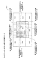
次に、各画像処理部が周辺画素データを交換する経路について説明する。図6は、各画像ブロックDInの周辺画素データの交換経路を模式的に説明する説明図である。実際は、各画像処理部のデータ交換部が互いに接続されており周辺画素データを交換するが、理解を容易にするため、各画像処理部が処理を担当する各画像ブロックDIn1〜9によって周辺画素データの交換経路について模式的に説明する。図6に示した矢印は、各画像処理部間の周辺画素データの交換経路を示しており、一回のデータ交換で双方向のデータ交換が可能である。また本実施例では、周辺画素データの交換は2回のタイミングで行われ、図6においては、1回目のデータ交換で使用する交換経路を実線の矢印で、2回目のデータ交換で使用する交換経路を破線の矢印で示した。 Next, a path through which each image processing unit exchanges peripheral pixel data will be described. FIG. 6 is an explanatory diagram schematically illustrating an exchange path of peripheral pixel data of each image block DIn. Actually, the data exchange units of the image processing units are connected to each other and exchange the peripheral pixel data. However, in order to facilitate understanding, the peripheral pixel data is processed by the image blocks DIn1 to DIn9 that each image processing unit is responsible for processing. The exchange route will be schematically described. The arrows shown in FIG. 6 indicate the exchange path of peripheral pixel data between the image processing units, and bidirectional data exchange is possible with one data exchange. In this embodiment, the neighboring pixel data is exchanged at two timings. In FIG. 6, the exchange path used in the first data exchange is indicated by a solid arrow, and the exchange used in the second data exchange. The route is indicated by a dashed arrow.
図6に示すように、例えば、画像ブロックDIn5(実際は第5画像処理部35)は、画像データDIn0における画像ブロックDInの位置関係として、上下左右に隣接する画像ブロックDIn2,DIn4,DIn6,DIn8の処理を担当する各画像処理部のデータ交換部と接続されている。そして、それらの画像処理部とだけ、周辺画素データ交換を行う。他の各画像処理部も同様に、画像ブロックの位置関係として、その画像処理部に対応する画像ブロックが、上下左右方向に隣接する画像ブロックに対応する画像処理部とだけ接続されており、周辺画素データの交換を行う。従って、例えば、DIn5(第5画像処理部35)のデータ交換部は4つの通信線で接続され、DIn1は2つ、DIn3は3つのデータ交換用の通信線で接続されている。本実施例においては、各画像処理部31〜39のデータ交換部はどれも、4つのデータ交換処理デバイスを備え、図6に示した通信経路の必要数に応じて、データ交換処理デバイスに通信線を接続することで、周辺画素データ交換用の通信経路が構成されている。
As shown in FIG. 6, for example, the image block DIn5 (actually the fifth image processing unit 35) includes, as the positional relationship of the image block DIn in the image data DIn0, the image blocks DIn2, DIn4, DIn6, and DIn8 that are adjacent vertically and horizontally. It is connected to the data exchange unit of each image processing unit in charge of processing. Then, peripheral pixel data exchange is performed only with these image processing units. Similarly, in the other image processing units, the image block corresponding to the image processing unit is connected only to the image processing unit corresponding to the image block adjacent in the vertical and horizontal directions as the positional relationship of the image blocks. Exchange pixel data. Therefore, for example, the data exchange unit of DIn5 (fifth image processing unit 35) is connected by four communication lines, two DIn1 and DIn3 are connected by three data exchange communication lines. In this embodiment, each of the data exchange units of the
次に、各画像処理部間で行う周辺画素データ交換処理の流れについて説明する。図7は周辺画素データ交換処理の流れについて説明したフローチャートである。周辺画素データ交換処理は、画像処理装置1における画像処理(図4参照)のサブルーチン(図4:ステップS140)として行われる。周辺画素データ交換処理が開始されると、最初に画像ブロックDInの位置関係として、上下方向に隣接する画像ブロックDInの画像処理を担当する各画像処理部同士で周辺画素データの交換を行う(ステップS142)。図8は、周辺画素データの交換の様子を示す説明図である。図8(a)は画像ブロックDIn1〜DIn9が各画像処理部に保存されている状態を示している。図8(b)は、ステップS142で説明した、画像ブロックDInの位置関係として、上下方向に隣接する各画像処理部同士で周辺画素データの交換を行っている様子を示す説明図である。図8(b)の点線で囲まれた部分が、上下に互いに隣接する画像ブロックDInの画像処理を担当する各画像処理部間で交換される周辺画素データを示す。図8(b)に示すように、例えば、画像ブロックDIn2の画像処理を担当する第2画像処理部32は、下方向に隣接する画像ブロックDIn5を担当する第5画像処理部35と互いに周辺画素データを交換し、画像ブロックDIn5の画像処理を担当する第5画像処理部35は、上方向および下方向に隣接する、画像ブロックDIn2及び画像ブロックDIn8をそれぞれ担当する第2画像処理部32,第8画像処理部38と互いに周辺画素データを交換する。
Next, a flow of peripheral pixel data exchange processing performed between the image processing units will be described. FIG. 7 is a flowchart for explaining the flow of the peripheral pixel data exchange process. The peripheral pixel data exchange processing is performed as a subroutine (FIG. 4: step S140) of image processing (see FIG. 4) in the
この時、例えば、画像ブロックDIn1は、画像ブロックDIn4が画像処理に必要とする周辺画像データをDIn4に送信するとともに、画像ブロックDIn5が画像処理に必要な周辺画素データのうち、画像ブロックDIn1に含まれる周辺画素データ(図8(b)の横線ハッチング部分)も同時に、画像ブロックDIn4に送信する。画像ブロックDIn4に対応する第4画像処理部34のデータ交換部341は、それらの周辺画素データを取得すると一時的に、第4画像処理部が備えるフレームメモリー344に記憶する。この場合、画像ブロックDIn1が画像ブロックDIn4に送信した周辺画素データのうち、画像ブロックDIn5が処理に必要とする周辺画素データは、画像ブロックDIn4が処理に必要とする周辺画素データの中に含まれる。つまり、説明の便宜上、この二つの周辺画素データは別個のものとして説明したが、実際は、画像ブロックDIn1は画像ブロックDIn4に対して、画像ブロックDIn4が処理に必要な周辺画素データを送信する。 At this time, for example, the image block DIn1 transmits the peripheral image data required for the image processing by the image block DIn4 to the DIn4, and the image block DIn5 is included in the image block DIn1 among the peripheral pixel data required for the image processing. The neighboring pixel data (horizontal line hatched portion in FIG. 8B) is also transmitted to the image block DIn 4 at the same time. The data exchanging unit 341 of the fourth image processing unit 34 corresponding to the image block DIn4 temporarily stores the peripheral pixel data in the frame memory 344 included in the fourth image processing unit. In this case, among the peripheral pixel data transmitted from the image block DIn1 to the image block DIn4, the peripheral pixel data required for the processing by the image block DIn5 is included in the peripheral pixel data required for the processing by the image block DIn4. . That is, for convenience of explanation, the two neighboring pixel data have been described as separate, but actually, the image block DIn1 transmits the neighboring pixel data necessary for the processing to the image block DIn4.
各画像処理部が上下方向の周辺画素データの交換を完了すると、各データ交換部が、これをタイミング指示部60に通知する。タイミング指示部60は、各データ交換部における周辺画素データの交換の状況を解析し、全ての画像処理部において周辺画素データの交換が終了したと判断した場合(ステップS144:Yes)、続いて、画像ブロックDInの位置関係として、左右方向に隣接する画像ブロックDInの画像処理を担当する各画像処理部同士で周辺画素データの交換を行う(ステップS146)。図8(c)は、左右方向に隣接する画像ブロックDInの画像処理を担当する各画像処理部同士で周辺画素データの交換を行っている様子を示す説明図である。図8(c)の斜線のハッチングを施した部分が、図8(b)で説明した、上下方向に隣接する画像ブロック同士での周辺画素データの交換により、各画像ブロックDInが取得した周辺画素データである。また、図8(c)の各画像ブロックDInの点線で囲まれた部分が、左右方向に互いに隣接する画像ブロックDInの画像処理を担当する各画像処理部間で交換される周辺画素データを示す。図8(c)に示すように、例えば、画像ブロックDIn4は、右方向に隣接する画像ブロックDIn5と互いに周辺画素データを交換し、画像ブロックDIn5は、左右方向に隣接する画像ブロックDIn4,画像ブロックDIn6とそれぞれ周辺画素データを交換する。
When each image processing unit completes the exchange of the peripheral pixel data in the vertical direction, each data exchange unit notifies the
この時、画像ブロックDIn4は、画像ブロックDIn5が処理に必要とする画像ブロックDIn4に含まれる周辺画素データを送信するとともに、ステップS142で画像ブロックDIn4が画像ブロックDIn1から取得した周辺画素データのうち、画像ブロックDIn5(第5画像処理部35)が処理に必要とする周辺画素データ(図8(c)参照)も同時に送信する。つまり、画像ブロックDIn4(第4画像処理部34)は、画像ブロックDIn1(第1画像処理部31)から画像ブロックDIn5(第5画像処理部35)に送信される周辺画素データを仲介する。換言すれば、画像ブロックDIn4(第4画像処理部34)は、画像ブロックDIn5(第5画像処理部35)が周辺画素として扱う画素の少なくとも一部のデータを、画像ブロックDIn1(第1画像処理部31)から、画像ブロックDIn5(第5画像処理部35)に向けて仲介する。第4画像処理部34が第1画像処理部31から第5画像処理部35に送信される周辺画素データを仲介することに着目した場合、第5画像処理部35が、特許請求の範囲に記載の「第1の部分画像について画像処理を行う際、当該第1の部分画像と隣り合った他の部分画像を構成する画素のうち、少なくとも第1の部分画像に隣接する領域の画素のデータを取得して、周辺画素のデータとして、画像処理に用いる第1の画像処理ユニット」に相当し、第4画像処理部34が、特許請求の範囲に記載の「第1の部分画像とは異なる第2の部分画像について画像処理を行うと共に、第1の画像処理ユニットが周辺画素として扱う画素の少なくとも一部のデータを、第1の画像処理ユニットが扱う部分画像に隣り合った部分画像を処理する画像処理ユニットから、第1の画像処理ユニットに向けて仲介する第2の画像処理ユニット」に相当する。また、他の画像処理部間においても、同様の方法によって周辺画素データの交換が行われる。例えば、画像ブロックDIn1が処理に必要とする画像ブロックDIn5に含まれる周辺画素データは、ステップS142の処理で画像ブロックDIn2に送信され、ステップS146の処理で画像ブロックDIn2から画像ブロックDIn1に送信される。このようにして、各画像処理部が左右方向の周辺画素データの交換を完了すると、各データ交換部が、これをタイミング指示部60に通知する。タイミング指示部60は、各データ交換部における周辺画素データの交換の状況を解析し、全ての画像処理部において周辺画素データの交換が終了したと判断した場合(ステップS148:Yes)、周辺画素データ交換処理は終了する。図8(d)は、上記図8(b),(c)で説明した周辺画素データ交換処理によって交換された周辺画素データを示す説明図である。斜線のハッチングが施された部分が、周辺画素データ交換処理によって、各画像ブロックDInが取得した周辺画素データである。このように周辺画素データを交換することで、各画像処理部が画像処理に必要な周辺画素データを交換することが可能である。
At this time, the image block DIn4 transmits the peripheral pixel data included in the image block DIn4 required for processing by the image block DIn5, and among the peripheral pixel data acquired by the image block DIn4 from the image block DIn1 in step S142, The peripheral pixel data (see FIG. 8C) required for processing by the image block DIn5 (fifth image processing unit 35) is also transmitted simultaneously. That is, the image block DIn4 (fourth image processing unit 34) mediates peripheral pixel data transmitted from the image block DIn1 (first image processing unit 31) to the image block DIn5 (fifth image processing unit 35). In other words, the image block DIn4 (fourth image processing unit 34) uses at least part of the data handled by the image block DIn5 (fifth image processing unit 35) as peripheral pixels as the image block DIn1 (first image processing unit). From the unit 31) to the image block DIn5 (fifth image processing unit 35). When attention is paid to the fact that the fourth image processing unit 34 mediates peripheral pixel data transmitted from the first
以上説明したように、第1実施例における周辺画素データの交換方法を用いることで、上下方向(図7:ステップS142)と左右方向(図7:ステップS146)の合計2回の周辺画素データの交換で、各画像処理部が画像処理に必要な周辺画素データの交換が可能であり、周辺画素データの交換を高速に行うことが可能である。また、図6からわかるように、各画像処理部は、全ての画像処理部と接続されている必要はなく、画像ブロックDInの位置関係として、上下左右に隣接する画像ブロックDInの画像処理を担当する画像処理部と接続されていればよい。つまり、1つの画像処理部は最大で4つの画像処理部と接続されていればよい。従って、各画像処理部が、隣接する全ての画像処理部と、各々に周辺画素データ交換用のラインで接続されていて、それぞれ直接に通信をして周辺画素データを交換する場合と比べて、画像処理装置の構造上、トランシーバー数、配線数、デバイスのピン数等を減少させることができる。なお、特許請求の範囲との対応関係としては、画像ブロックDIn1〜9が、特許請求の範囲に記載の部分画像に相当し、各画像処理部が、特許請求の範囲に記載の画像処理ユニットに相当し、画像合成部40が、特許請求の範囲に記載の画像出力ユニットに相当する。
As described above, by using the peripheral pixel data exchanging method in the first embodiment, the peripheral pixel data of the vertical direction (FIG. 7: step S142) and the horizontal direction (FIG. 7: step S146) are totaled twice. By exchanging, it is possible for each image processing unit to exchange peripheral pixel data necessary for image processing, and it is possible to exchange peripheral pixel data at high speed. Further, as can be seen from FIG. 6, each image processing unit does not have to be connected to all the image processing units, and is responsible for image processing of the image block DIn that is adjacent vertically and horizontally as the positional relationship of the image block DIn. It is only necessary to be connected to the image processing unit. That is, it is sufficient that one image processing unit is connected to a maximum of four image processing units. Therefore, each image processing unit is connected to all adjacent image processing units by a line for exchanging peripheral pixel data, and compared with a case where each of the image processing units directly communicates and exchanges peripheral pixel data, Due to the structure of the image processing apparatus, the number of transceivers, the number of wires, the number of pins of the device, and the like can be reduced. In addition, as a correspondence relationship with the claims, the image blocks DIn1 to 9 correspond to the partial images described in the claims, and each image processing unit corresponds to the image processing unit described in the claims. The
また、第1実施例では、画像データDIn0を3×3に分割した例で説明したが、より多くの分割数、例えば、4×4や、10×10、16×9などに分割しても、第1実施例と同様の効果を得ることができる。つまり、画像ブロックDInの位置関係として、各画像ブロックDInの処理を担当する各画像処理部が、上下左右に隣接する画像ブロックDInの画像処理を担当する画像処理部と接続されていれば、1つの画像処理部は最大で4つの画像処理部との接続によって、上下方向と左右方向の合計2回の周辺画素データの交換で、各画像処理部が画像処理に必要な周辺画素データの交換が可能であり、周辺画素データの交換を高速に行うことができる。 In the first embodiment, the example in which the image data DIn0 is divided into 3 × 3 has been described. However, the image data DIn0 may be divided into a larger number of divisions, for example, 4 × 4, 10 × 10, 16 × 9, or the like. The same effects as in the first embodiment can be obtained. That is, as the positional relationship of the image block DIn, if each image processing unit in charge of processing of each image block DIn is connected to the image processing unit in charge of image processing of the image block DIn adjacent in the vertical and horizontal directions, 1 By connecting a maximum of four image processing units to a maximum of four image processing units, the peripheral pixel data is exchanged in a total of two times in the vertical and horizontal directions. It is possible to exchange the peripheral pixel data at high speed.
本実施例では、複数の画像処理部のうち、他の画像処理部が処理に必要な周辺画素データを仲介する画像処理部と、仲介しない画像処理部とが存在するが、全ての画像処理部が仲介を行う機能を備え、処理を担当する画像ブロックDInの画像データDIn0における配置関係によって、必要に応じ仲介処理を行うとしてもよい。この場合、複数の画像処理部は、少なくとも、「第1の部分画像について画像処理を行う際、当該第1の部分画像と隣り合った他の部分画像を構成する画素のうち、少なくとも第1の部分画像に隣接する領域の画素のデータを取得して、前記周辺画素のデータとして、画像処理に用いる第1の画像処理ユニット」と、「第1の部分画像とは異なる第2の部分画像について画像処理を行うと共に、第1の画像処理ユニットが周辺画素として扱う画素の少なくとも一部のデータを、第1の画像処理ユニットが扱う部分画像に隣り合った部分画像を処理する画像処理ユニットから、前記第1の画像処理ユニットに向けて仲介する第2の画像処理ユニット」とを含んでいればよい。 In this embodiment, among the plurality of image processing units, there are an image processing unit that mediates peripheral pixel data necessary for processing by other image processing units, and an image processing unit that does not mediate, but all image processing units May have an intermediary function, and an intermediary process may be performed according to the arrangement relationship in the image data DIn0 of the image block DIn in charge of the process. In this case, the plurality of image processing units at least “when performing image processing on the first partial image, at least the first of the pixels constituting the other partial image adjacent to the first partial image. The pixel data of the area adjacent to the partial image is acquired, and as the peripheral pixel data, the “first image processing unit used for image processing” and “the second partial image different from the first partial image” From the image processing unit that performs image processing and processes at least a part of data of pixels handled by the first image processing unit as peripheral pixels, a partial image adjacent to the partial image handled by the first image processing unit, And a second image processing unit that mediates toward the first image processing unit.
B.第2実施例:
次に第2実施例について説明する。第1実施例と第2実施例との違いは、各画像ブロックDInの周辺画素データの交換経路である。またそれに伴って、周辺画素データの交換の流れも第1実施例と第2実施例では異なる。第2実施例における周辺画素データの交換経路は、画像ブロックDInの位置関係において、画像ブロックDIn1〜9間を、1経路で、かつ、同じ経路を2度通ることなく結ぶように交換経路を構成する。換言すれば、画像ブロックDIn1〜9間を、いわゆる「一筆書き(an Eulerian path(閉路の場合)又は a traversable figure(始点と終点が異なる場合))」の要領で経路構成する。その一例を図9に示す。図9(a)は、第2実施例における、各画像ブロックDInの周辺画素データの交換経路の一例を示した説明図である。画像ブロック(実際は画像処理部)同士は、交換経路で結ばれている。この交換経路は、画像ブロック(実際は画像処理部)同士が互いに直接に周辺画素データを取得する経路である。なお、この交換経路が特許請求の範囲に記載のデータ取得経路に相当する。図9(a)に示すように、周辺画素の交換経路は、画像ブロックDIn1〜9間を、1つの経路で、かつ、同じ画像ブロックを2度通ることなく結ぶように構成されている。このような交換経路を用いて、各画像処理部は周辺画素データを交換する。なお、図9(a)に示した矢印は、各画像処理部間の周辺画素データの交換経路を示しており、一回のデータ交換で双方向のデータ交換が可能である。なお、一筆書きが可能である条件として、「頂点から出ている線の数が奇数本である頂点の数が、0個(閉路)か2個(始点と終点が異なる)の場合」に一筆書きが可能である。これを本実施例に置き換えると、「画像処理部に接続されている周辺画素データ交換経路の数が奇数個である画像処理部の数が、0個、若しくは2個の場合」に、このような一筆書きの経路構成が可能である。換言すれば、「各データ交換部のうち、奇数個の他のデータ交換部と直接にデータ交換をするデータ交換部の数が0個または2個の場合」に、一筆書きの経路構成が可能である。このように、各画像処理ユニットとデータ取得経路とから構成され、全ての画像処理ユニットを1度ずつ通る経路が形成される。なお、このような一筆書きが可能な一連の周辺画素データの交換経路が、特許請求の範囲に記載のデータ通信経路に相当する。
B. Second embodiment:
Next, a second embodiment will be described. The difference between the first embodiment and the second embodiment is the exchange path of the peripheral pixel data of each image block DIn. Accordingly, the flow of exchanging peripheral pixel data is also different between the first embodiment and the second embodiment. The peripheral pixel data exchange path in the second embodiment is configured such that the image blocks DIn1 to 9 are connected by one path and without passing through the same path twice in the positional relationship of the image block DIn. To do. In other words, a path is constructed between the image blocks DIn1 to DIn9 in the manner of a so-called “one stroke writing (an Eulerian path (when closed) or a traversable figure (when starting point and ending point are different))”. An example is shown in FIG. FIG. 9A is an explanatory diagram showing an example of an exchange path of peripheral pixel data of each image block DIn in the second embodiment. Image blocks (actually image processing units) are connected by an exchange path. This exchange path is a path through which image blocks (actually image processing units) directly acquire peripheral pixel data. This exchange route corresponds to the data acquisition route described in the claims. As shown in FIG. 9A, the replacement path of the peripheral pixels is configured to connect the image blocks DIn1 to 9 with one path and without passing through the same image block twice. Using such an exchange path, each image processing unit exchanges peripheral pixel data. Note that the arrows shown in FIG. 9A indicate the exchange path of the peripheral pixel data between the image processing units, and bidirectional data exchange is possible with one data exchange. In addition, as a condition that a single stroke can be drawn, one stroke is drawn when “the number of vertices with odd numbers of vertices is 0 (closed) or 2 (start point and end point are different)”. Can be written. When this is replaced with the present embodiment, “when the number of image processing units having an odd number of peripheral pixel data exchange paths connected to the image processing unit is 0 or 2,” A simple one-stroke path configuration is possible. In other words, one-stroke path configuration is possible when “the number of data exchange units that directly exchange data with an odd number of other data exchange units among the data exchange units is 0 or 2”. It is. In this way, each image processing unit and the data acquisition path are configured, and a path that passes through all the image processing units once is formed. Note that such a series of peripheral pixel data exchange paths that allow one-stroke writing correspond to the data communication paths described in the claims.
次に、周辺画素データの交換の方法について説明する。例えば、画像ブロックDIn5の画像処理に必要な、画像ブロックDIn1に含まれる周辺画素データ(図5参照)を交換する場合、DIn1→DIn2→DIn3→DIn6→DIn5の交換経路で、DIn5に周辺画素データが送信される。また、上述したように、データ交換は一回のデータ交換で双方向のデータ交換が可能である。例えば、最も周辺画素データの交換経路として遠いDIn1とDIn4(又は、DIn6とDIn9)とは、5回のタイミングでデータ交換を行うことによって周辺画素データの交換が可能である。 Next, a method for exchanging peripheral pixel data will be described. For example, when the peripheral pixel data (see FIG. 5) included in the image block DIn1 necessary for image processing of the image block DIn5 is exchanged, the peripheral pixel data is transferred to DIn5 through the exchange path of DIn1 → DIn2 → DIn3 → DIn6 → DIn5. Is sent. In addition, as described above, data exchange can be performed bidirectionally with a single data exchange. For example, DIn1 and DIn4 (or DIn6 and DIn9) that are farthest as the peripheral pixel data exchange path can exchange the peripheral pixel data by performing data exchange at five times.
図9(b)は、DIn1とDIn4がデータ交換するために必要なデータ交換のタイミングと、その交換の向きについて説明した説明図である。説明の便宜上、DIn1からDIn4までの周辺画素データの交換経路を直線状に表現した。実線の矢印は、DIn4が必要なDIn1に含まれる周辺画素データを、DIn1から順にDIn2、DIn3、DIn6、DIn5を経由してDIn4に送信されている様子を示している。一方、破線の矢印は、DIn1が必要なDIn4に含まれる周辺画素データを、DIn4から順にDIn5、DIn6、DIn3、DIn2を経由してDIn1に送信されている様子を示している。 FIG. 9B is an explanatory diagram illustrating the timing of data exchange required for data exchange between DIn1 and DIn4 and the direction of the exchange. For convenience of explanation, the exchange path of peripheral pixel data from DIn1 to DIn4 is expressed in a straight line. A solid line arrow indicates that peripheral pixel data included in DIn1 that requires DIn4 is transmitted to DIn4 sequentially from DIn1 via DIn2, DIn3, DIn6, and DIn5. On the other hand, the broken arrow indicates that the peripheral pixel data included in DIn4 that requires DIn1 is transmitted to DIn1 sequentially from DIn4 via DIn5, DIn6, DIn3, and DIn2.
矢印の上に付した数字はデータ交換が行われるタイミングを示している。つまり、1回目のデータ交換のタイミングで、DIn1→DIn2のデータ交換と、DIn4→DIn5のデータ交換が行われる。2回目のデータ交換のタイミングで、DIn2→DIn3のデータ交換と、DIn5→DIn6のデータ交換が行われる。このように周辺画素データの交換を行うことによって、DIn1とDIn4とは5回のデータ交換のタイミングで、周辺画素データの交換を行うことができる。また、この5回のデータ交換のタイミング内で、例えば、DIn2とDIn5や、DIn3とDIn5などが、周辺画素データの交換を、他の画像ブロックDInを経由して行うことが可能である。勿論、直接に周辺画素データを交換するDIn1とDIn2や、DIn5とDIn4などは、この5回のデータ交換のタイミング内で直接に周辺画素データの交換が可能である。 The numbers above the arrows indicate the timing at which data exchange is performed. That is, at the timing of the first data exchange, data exchange of DIn1 → DIn2 and data exchange of DIn4 → DIn5 are performed. At the timing of the second data exchange, data exchange of DIn2-> DIn3 and data exchange of DIn5-> DIn6 are performed. By exchanging the peripheral pixel data in this way, DIn1 and DIn4 can exchange the peripheral pixel data at the timing of data exchange five times. Further, within the timing of the five data exchanges, for example, DIn2 and DIn5, DIn3 and DIn5, and the like can exchange peripheral pixel data via other image blocks DIn. Of course, DIn1 and DIn2 and DIn5 and DIn4 that directly exchange peripheral pixel data can directly exchange the peripheral pixel data within the timing of the five data exchanges.
他の各画像処理部が必要とする周辺画素データについても、同様に、図9(a)に示した交換経路上を介し、他の画像処理部を経由して、その周辺画像データを必要とする画像処理部に送信される。また図9(a)に示した交換経路は、一筆書きで言えば、「始点と終点とが異なる場合」に相当する。この場合、各画像処理部は、双方向に周辺画素データを交換して、各画像処理部が必要な周辺画素データを取得する。なお、交換経路を、一筆書きで言う「閉路」で構成する事も可能であり、この場合は、交換経路はループ状となるので、各画像処理部が交換経路上を一方向のみに周辺画素データを送信し、各画像処理部が処理に必要な周辺画素データが当該画像処理部を通過する際に、その周辺画素データを取得(または参照)するとしてもよい。その具体的な経路については、後の変形例で説明する。 Similarly, the peripheral pixel data required by each of the other image processing units requires the peripheral image data via the other image processing unit via the exchange path shown in FIG. 9A. To the image processing unit. The exchange path shown in FIG. 9A corresponds to “when the start point and the end point are different” in a single stroke. In this case, each image processing unit exchanges peripheral pixel data bidirectionally, and each image processing unit acquires the necessary peripheral pixel data. Note that the exchange path can also be configured as a “closed circuit” in a single stroke. In this case, since the exchange path is a loop, each image processing unit has peripheral pixels in only one direction on the exchange path. The data may be transmitted, and each pixel processing unit may acquire (or refer to) the peripheral pixel data when the peripheral pixel data necessary for processing passes through the image processing unit. The specific route will be described in a later modification.
以上説明したように、第2実施例における周辺画素データの交換方法を用いることで、各画像処理部は、全ての画像処理部と接続されている必要はなく、1つ乃至2つの画像処理部と接続されていればよい。従って、第1実施例と比較してさらに、画像処理装置の構造上、トランシーバー数、配線数、デバイスのピン数等を減少させることができる。 As described above, by using the peripheral pixel data exchange method in the second embodiment, each image processing unit does not have to be connected to all the image processing units, and one or two image processing units. As long as it is connected. Therefore, compared with the first embodiment, the number of transceivers, the number of wires, the number of device pins, and the like can be further reduced due to the structure of the image processing apparatus.
C.変形例:
なお、この発明は上記の実施例や実施形態に限られるものではなく、その要旨を逸脱しない範囲において種々の態様において実施することが可能であり、例えば次のような変形も可能である。
C. Variation:
The present invention is not limited to the above-described examples and embodiments, and can be implemented in various modes without departing from the gist thereof. For example, the following modifications are possible.
(C1)変形例1:
上記実施例では、画像データDIn0を3×3に分割したが、4×4や、4×3など、M×N(M,Nは2以上の正の整数)に分割するとしても同様の効果を得ることができる。分割数を多くした場合、各画像処理部が処理をする画素数が減るので、画像処理の処理速度が、上記実施例と比較してさらに高速となる。
(C1) Modification 1:
In the above embodiment, the image data DIn0 is divided into 3 × 3, but the same effect can be obtained even if the image data is divided into M × N (M and N are positive integers of 2 or more) such as 4 × 4 and 4 × 3. Can be obtained. When the number of divisions is increased, the number of pixels processed by each image processing unit is reduced, so that the processing speed of image processing is further increased compared to the above-described embodiment.
(C2)変形例2:
上記第1実施例では、周辺画素データ交換処理は上下方向(垂直方向)を先に行い、後に左右方向(水平方向)に行ったが、変形例2として、先に左右方向(水平方向)を行い、後に上下方向(垂直方向)を行ってもよい。このようにしても、上記第1実施例と同様の効果を得ることが可能である。
(C2) Modification 2:
In the first embodiment, the peripheral pixel data exchange processing is performed in the up-down direction (vertical direction) first and then in the left-right direction (horizontal direction). However, as Modification 2, the left-right direction (horizontal direction) is first performed. It may be performed later, and the vertical direction (vertical direction) may be performed later. Even if it does in this way, it is possible to acquire the effect similar to the said 1st Example.
(C3)変形例3:
上記実施例2では、図9に示した周辺画素データの交換経路によって周辺画素データを交換したが、これに限ることなく、DIn0を、3×3や、それ以外の分割数に分割することが可能である。例えば図10に示した交換経路を構成して周辺画素データを交換することが可能である。図10(a)および図10(b)に示した交換経路は、各画像ブロックDIn間を、1つの経路で、かつ、同じ経路を2度通ることなく結ぶように構成されている。図10(b)は、上記で説明した「閉路」の経路構成である。このように構成した交換経路によって周辺画素データを交換する場合、上述したように、各データ交換部は、周辺画素データを経路上の一方向のみに送信すればよい。このような経路構成としても、上記第2実施例と同様の効果を得ることが可能である。
(C3) Modification 3:
In the second embodiment, the peripheral pixel data is exchanged by the peripheral pixel data exchange path shown in FIG. 9, but the present invention is not limited to this, and DIn0 may be divided into 3 × 3 or other division numbers. Is possible. For example, it is possible to exchange peripheral pixel data by configuring the exchange path shown in FIG. The exchange paths shown in FIGS. 10A and 10B are configured to connect the image blocks DIn with one path and without passing the same path twice. FIG. 10B shows the “ closed circuit” path configuration described above. When the surrounding pixel data is exchanged by the exchange path configured as described above, as described above, each data exchange unit may transmit the surrounding pixel data only in one direction on the path. Even with such a path configuration, it is possible to obtain the same effect as in the second embodiment.
(C4)変形例4:
上記実施例では、各画像処理部に部分画像データが蓄積された後にタイミング指示部がデータ交換開始の指示を各画像処理部に出力していたが、本変形例では、タイミング指示部60は、各画像処理部31〜39における画像データの蓄積の状況を解析し、第1ないし第9画像処理部31〜39のうち、データ交換が可能になった処理部に対してデータ交換の開始を指示する。このようにデータ交換をすると、上記実施例と比較して、さらにデータ交換を高速に行うことが可能である。
(C4) Modification 4:
In the above embodiment, after the partial image data is accumulated in each image processing unit, the timing instruction unit outputs an instruction to start data exchange to each image processing unit. However, in this modification, the
(C5)変形例5:
上記実施例では、映像ストレージSt1〜St9から、画像ブロックDIn1〜9が画像入力部21〜29を介してプロジェクターに入力されるとしたが、変形例5においては、プロジェクターに画像データDIn0が入力され、画像処理装置1aにおいて画像データDIn0を画像ブロックDIn1〜DIn9に分割する。図11は、変形例5における画像処理装置1aの構成を説明する説明図である。第1実施例と同じ機能を備える機能部には同じ符号を付している。図11に示すように、画像データDIn0を記憶している映像ストレージSt0から画像像入力部20aに画像データDIn0が入力され、画像処理装置1aが備える画像分割部90が画像データDIn0を画像ブロックDIn1〜DIn9に分割し、各画像処理部31〜39に送信する。以降の処理は第1実施例と同様の処理である。このような構成にしても上記実施例と同様の効果が得られる。
(C5) Modification 5:
In the above embodiment, the image blocks DIn1 to 9 are input from the video storages St1 to St9 to the projector via the
(C6)変形例6:
上記実施例では、データ交換部は、他の画像処理部と周辺画素データのやり取りをするデータ交換処理デバイスを複数備えることによって、他の複数の画像処理部とデータの交換を行っていたが、変形例6として、データ交換の方向を切り換える切り換えスイッチSWを備えることにより、データ交換処理デバイスの数を上記実施例より少なくする構成としてもよい。
(C6) Modification 6:
In the above embodiment, the data exchange unit exchanges data with a plurality of other image processing units by providing a plurality of data exchange processing devices that exchange peripheral pixel data with other image processing units. As a sixth modification, a configuration is possible in which the number of data exchange processing devices is smaller than that of the above-described embodiment by providing a changeover switch SW for switching the direction of data exchange.
図12は、変形例6の具体例を説明する説明図である。図12に示すように、画像処理装置は、上記第1実施例と同様に、各画像処理部は、上下左右に隣接している画像処理部と接続されている。さらに、変形例6の特徴として、接続経路上に、必要に応じて、切り換えスイッチSWを備える。図12においては、切り換えスイッチSWは、画像処理部の外部に設ける構成であるが、画像処理部の内部に設ける構成としてもよい。図12の具体例の場合は、各画像処理部間で周辺画素データを互いに交換する場合は、データ交換をするタイミングで、必要に応じて切り換えスイッチSWを切り換えることにより、最大で4つの画像処理部との通信が可能となり、第1実施例と実質的に同等のデータ交換が可能である。このような構成にすることで、画像処理部が4つのデータ交換処理デバイスを備える必要がなく、データ交換処理デバイスの数を減らすことができる。 FIG. 12 is an explanatory diagram illustrating a specific example of the sixth modification. As shown in FIG. 12, in the image processing apparatus, as in the first embodiment, each image processing unit is connected to adjacent image processing units in the vertical and horizontal directions. Furthermore, as a feature of the modification 6, a changeover switch SW is provided on the connection path as necessary. In FIG. 12, the selector switch SW is provided outside the image processing unit, but may be provided inside the image processing unit. In the case of the specific example of FIG. 12, when exchanging neighboring pixel data between the image processing units, a maximum of four image processes can be performed by switching the changeover switch SW as necessary at the time of data exchange. Communication is possible, and data exchange substantially equivalent to that of the first embodiment is possible. With this configuration, it is not necessary for the image processing unit to include four data exchange processing devices, and the number of data exchange processing devices can be reduced.
また、各画像処理部との接続経路を第2実施例と同様に所謂一筆書きの構成とし、2つ以上の画像処理部とデータ交換を行う画像処理部が、切り換えスイッチSWを備え、必要に応じて、データ交換のタイミングで切り換えスイッチSWを切り換えるとしてもよい。このようにすることで、データ交換処理デバイスの数を上記第2実施例と比べて減らすことが可能である。 In addition, the connection path to each image processing unit is a so-called one-stroke writing configuration as in the second embodiment, and the image processing unit that exchanges data with two or more image processing units includes a changeover switch SW and is necessary. Accordingly, the selector switch SW may be switched at the data exchange timing. In this way, the number of data exchange processing devices can be reduced as compared with the second embodiment.
1…画像処理装置
10…画像入力部
20…画像分割部
31〜39…第1〜第9画像処理部
40…画像合成部
50…画像出力部
60…タイミング指示部
71…CPU
80…フレームメモリー
81…入力インタフェース
83…出力インタフェース
85…指示入力インタフェース
341…データ交換部
344…フレームメモリー
351…分割画像入力部
352…データ交換部
353…フレームメモリー制御部
354…フレームメモリー
355…フィルター処理部
356…分割画像出力部
DIn0…画像データ
DIn1〜9…画像ブロック
DOut0…画像データ
St1〜St9…映像ストレージ
SW…切り換えスイッチ
PC1〜PC9…コンピューター
DESCRIPTION OF
DESCRIPTION OF
Claims (4)
前記画像データに対応した表示画像を水平方向および垂直方向に二次元的に分割した各部分画像に対応して設けられ、該部分画像に対応した画像データを入力し、該部分画像を構成する各画素のデータを、該部分画像の外側の前記部分画像の画素データである周辺画素データを参照して処理する複数の画像処理ユニットと、
該画像処理ユニットによって前記画像処理が行われた後の画素のデータを用いて、表示用画像データを出力する画像出力ユニットと
を備え、
前記複数の画像処理ユニットの各々は、
前記画像処理に先立つ2回のタイミングの各々で、前記各画像処理ユニットに水平方向または垂直方向にそれぞれ隣接する画像処理ユニットとの間で、前記周辺画素データのやり取りをし、
1回目のタイミングにおいて、該画像処理ユニットに水平方向または垂直方向のいずれか一方に隣接する前記画像処理ユニットと、互いに、前記周辺画素データをやり取りし、
前記1回目のタイミングとは別の2回目のタイミングで、該画像処理ユニットに水平方向または垂直方向のいずれか他方に隣接する前記画像処理ユニットと、互いに、前記周辺画素データをやり取りし、
前記2回のやり取りにより取得された、当該画像処理ユニットに対応する前記部分画像に対角方向に隣接する対角隣接部分画像の周辺画素データを含んで、前記画像処理を行なう
画像処理装置。 An image processing apparatus that processes image data representing an image composed of a plurality of pixels,
The display image corresponding to the image data is provided corresponding to each partial image obtained by two-dimensionally dividing the display image in the horizontal direction and the vertical direction, and the image data corresponding to the partial image is input to configure each partial image. A plurality of image processing units that process pixel data with reference to peripheral pixel data that is pixel data of the partial image outside the partial image ;
An image output unit that outputs image data for display using pixel data after the image processing is performed by the image processing unit;
Each of the plurality of image processing units is
At each of the two timings prior to the image processing, the peripheral pixel data is exchanged with the image processing units respectively adjacent to the image processing units in the horizontal direction or the vertical direction,
At the first timing, the peripheral pixel data is exchanged with the image processing unit adjacent to the image processing unit in either the horizontal direction or the vertical direction,
The peripheral pixel data is exchanged with the image processing unit adjacent to the image processing unit in either the horizontal direction or the vertical direction at a second timing different from the first timing,
An image processing apparatus that performs the image processing including peripheral pixel data of a diagonally adjacent partial image that is acquired by the two-time exchange and that is adjacent to the partial image corresponding to the image processing unit in a diagonal direction .
前記画像データを入力する画像データ入力部と、
前記画像データに対応した前記表示画像を二次元的に分割して複数の前記部分画像とし、該各部分画像を前記各画像処理ユニットに入力する画像分割部と
を備える画像処理装置。 The image processing apparatus according to claim 1, further comprising:
An image data input unit for inputting the image data;
An image processing apparatus comprising: an image dividing unit configured to two-dimensionally divide the display image corresponding to the image data into a plurality of partial images and input the partial images to the image processing units.
前記各画像処理ユニットが前記周辺画素データのやり取りをする、時分割された複数のタイミングを制御するタイミング制御部を備える画像処理装置。 The image processing apparatus according to claim 1 , further comprising:
An image processing apparatus comprising: a timing control unit that controls a plurality of time-divided timings at which the image processing units exchange the peripheral pixel data.
前記複数の画像処理ユニットの各々は、
前記画像処理に先立つ2回のタイミングの各々で、前記各画像処理ユニットに水平方向または垂直方向にそれぞれ隣接する画像処理ユニットとの間で、前記周辺画素データのやり取りをし、
1回目のタイミングにおいて、該画像処理ユニットに水平方向または垂直方向のいずれか一方に隣接する前記画像処理ユニットと、互いに、前記周辺画素データをやり取りし、
前記1回目のタイミングとは別の2回目のタイミングで、該画像処理ユニットに水平方向または垂直方向のいずれか他方に隣接する前記画像処理ユニットと、互いに、前記周辺画素データをやり取りし、
前記2回のやり取りにより取得された、当該画像処理ユニットに対応する前記部分画像に対角方向に隣接する対角隣接部分画像の周辺画素データを含んで、前記画像処理を行なう
画像処理方法。 Image data representing an image composed of a plurality of pixels is provided corresponding to each partial image obtained by two-dimensionally dividing the display image corresponding to the image data in the horizontal direction and the vertical direction. A plurality of image processing units that input the processed image data and process the data of each pixel constituting the partial image with reference to peripheral pixel data that is pixel data of the partial image outside the partial image An image processing method for processing,
Each of the plurality of image processing units is
At each of the two timings prior to the image processing, the peripheral pixel data is exchanged with the image processing units respectively adjacent to the image processing units in the horizontal direction or the vertical direction,
At the first timing, the peripheral pixel data is exchanged with the image processing unit adjacent to the image processing unit in either the horizontal direction or the vertical direction,
The peripheral pixel data is exchanged with the image processing unit adjacent to the image processing unit in either the horizontal direction or the vertical direction at a second timing different from the first timing,
An image processing method for performing the image processing including peripheral pixel data of a diagonally adjacent partial image diagonally adjacent to the partial image corresponding to the image processing unit acquired by the two exchanges .
Priority Applications (2)
| Application Number | Priority Date | Filing Date | Title |
|---|---|---|---|
| JP2009264631A JP5756594B2 (en) | 2009-11-20 | 2009-11-20 | Image processing apparatus and image processing method |
| US12/902,644 US8446418B2 (en) | 2009-11-20 | 2010-10-12 | Image processing apparatus and image processing method |
Applications Claiming Priority (1)
| Application Number | Priority Date | Filing Date | Title |
|---|---|---|---|
| JP2009264631A JP5756594B2 (en) | 2009-11-20 | 2009-11-20 | Image processing apparatus and image processing method |
Publications (3)
| Publication Number | Publication Date |
|---|---|
| JP2011108135A JP2011108135A (en) | 2011-06-02 |
| JP2011108135A5 JP2011108135A5 (en) | 2013-01-10 |
| JP5756594B2 true JP5756594B2 (en) | 2015-07-29 |
Family
ID=44061760
Family Applications (1)
| Application Number | Title | Priority Date | Filing Date |
|---|---|---|---|
| JP2009264631A Expired - Fee Related JP5756594B2 (en) | 2009-11-20 | 2009-11-20 | Image processing apparatus and image processing method |
Country Status (2)
| Country | Link |
|---|---|
| US (1) | US8446418B2 (en) |
| JP (1) | JP5756594B2 (en) |
Families Citing this family (5)
| Publication number | Priority date | Publication date | Assignee | Title |
|---|---|---|---|---|
| JP5939572B2 (en) * | 2012-07-11 | 2016-06-22 | 国立大学法人東京農工大学 | Data processing device |
| US10019775B2 (en) | 2015-04-30 | 2018-07-10 | Honeywell International Inc. | Method and system for scalable, radiation-tolerant, space-rated, high integrity graphics processing unit |
| JP2017191145A (en) * | 2016-04-11 | 2017-10-19 | キヤノン株式会社 | Image processing apparatus, image processing method, and program |
| JPWO2019111815A1 (en) * | 2017-12-06 | 2020-12-17 | シャープ株式会社 | Video processing equipment and display equipment |
| CN109064987A (en) * | 2018-08-31 | 2018-12-21 | 深圳市华星光电技术有限公司 | Liquid crystal display panel and liquid crystal display device with the liquid crystal display panel |
Family Cites Families (3)
| Publication number | Priority date | Publication date | Assignee | Title |
|---|---|---|---|---|
| JPH0740252B2 (en) * | 1986-03-08 | 1995-05-01 | 株式会社日立製作所 | Multi-processor system |
| US6731338B1 (en) * | 2000-01-10 | 2004-05-04 | Canon Kabushiki Kaisha | Reducing discontinuities in segmented SSAs |
| JP2006005524A (en) | 2004-06-16 | 2006-01-05 | Ricoh Co Ltd | Image processor and display |
-
2009
- 2009-11-20 JP JP2009264631A patent/JP5756594B2/en not_active Expired - Fee Related
-
2010
- 2010-10-12 US US12/902,644 patent/US8446418B2/en not_active Expired - Fee Related
Also Published As
| Publication number | Publication date |
|---|---|
| US20110122143A1 (en) | 2011-05-26 |
| US8446418B2 (en) | 2013-05-21 |
| JP2011108135A (en) | 2011-06-02 |
Similar Documents
| Publication | Publication Date | Title |
|---|---|---|
| JP5756594B2 (en) | Image processing apparatus and image processing method | |
| JP4219887B2 (en) | Image processing apparatus and image processing method | |
| JP5604894B2 (en) | Image processing apparatus, image processing method, and computer program | |
| US8305495B2 (en) | Video processing device, video display device, and video processing method | |
| JP5494013B2 (en) | Image processing apparatus, projection display apparatus, video display system, image processing method, computer program | |
| US7834914B2 (en) | Image pickup apparatus and signal processor | |
| JP6494294B2 (en) | Image processing apparatus and imaging system | |
| WO2017149591A1 (en) | Image processing device | |
| US10803589B2 (en) | Image processing device | |
| US20150381852A1 (en) | Data processing apparatus, data processing method, and storage medium | |
| JP4991907B2 (en) | Image processing apparatus and method for controlling image processing apparatus | |
| EP3232401A1 (en) | Image processing apparatus, image processing method, and program | |
| JP2015222932A (en) | Apparatus and method for image processing | |
| JP5533330B2 (en) | Data processing device | |
| JP6239843B2 (en) | Image processing apparatus and control method thereof | |
| JP2011108135A5 (en) | ||
| JP6338772B2 (en) | Image processing apparatus and image processing system | |
| JP6041630B2 (en) | Image processing device | |
| CN109391788A (en) | System for handling picture signal | |
| JP2013098966A (en) | Video processing system, video processing method, and computer program | |
| JP6723113B2 (en) | Image processing device | |
| JP2007243819A (en) | Image processing apparatus | |
| JP2008005230A (en) | Circuit for processing video signal, video display device and method for processing video signal | |
| JP2015089066A (en) | Image display device, control method of the same and program | |
| JP2017220821A (en) | Image processing device |
Legal Events
| Date | Code | Title | Description |
|---|---|---|---|
| A521 | Request for written amendment filed |
Free format text: JAPANESE INTERMEDIATE CODE: A523 Effective date: 20121116 |
|
| A621 | Written request for application examination |
Free format text: JAPANESE INTERMEDIATE CODE: A621 Effective date: 20121116 |
|
| A977 | Report on retrieval |
Free format text: JAPANESE INTERMEDIATE CODE: A971007 Effective date: 20130905 |
|
| A131 | Notification of reasons for refusal |
Free format text: JAPANESE INTERMEDIATE CODE: A131 Effective date: 20130917 |
|
| A521 | Request for written amendment filed |
Free format text: JAPANESE INTERMEDIATE CODE: A523 Effective date: 20131115 |
|
| A02 | Decision of refusal |
Free format text: JAPANESE INTERMEDIATE CODE: A02 Effective date: 20140121 |
|
| A521 | Request for written amendment filed |
Free format text: JAPANESE INTERMEDIATE CODE: A523 Effective date: 20140421 |
|
| A911 | Transfer to examiner for re-examination before appeal (zenchi) |
Free format text: JAPANESE INTERMEDIATE CODE: A911 Effective date: 20140430 |
|
| A912 | Re-examination (zenchi) completed and case transferred to appeal board |
Free format text: JAPANESE INTERMEDIATE CODE: A912 Effective date: 20140620 |
|
| A521 | Request for written amendment filed |
Free format text: JAPANESE INTERMEDIATE CODE: A523 Effective date: 20150320 |
|
| A61 | First payment of annual fees (during grant procedure) |
Free format text: JAPANESE INTERMEDIATE CODE: A61 Effective date: 20150601 |
|
| R150 | Certificate of patent or registration of utility model |
Ref document number: 5756594 Country of ref document: JP Free format text: JAPANESE INTERMEDIATE CODE: R150 |
|
| S531 | Written request for registration of change of domicile |
Free format text: JAPANESE INTERMEDIATE CODE: R313531 |
|
| R350 | Written notification of registration of transfer |
Free format text: JAPANESE INTERMEDIATE CODE: R350 |
|
| LAPS | Cancellation because of no payment of annual fees |