JP5725890B2 - Electrophotographic equipment - Google Patents
Electrophotographic equipment Download PDFInfo
- Publication number
- JP5725890B2 JP5725890B2 JP2011023858A JP2011023858A JP5725890B2 JP 5725890 B2 JP5725890 B2 JP 5725890B2 JP 2011023858 A JP2011023858 A JP 2011023858A JP 2011023858 A JP2011023858 A JP 2011023858A JP 5725890 B2 JP5725890 B2 JP 5725890B2
- Authority
- JP
- Japan
- Prior art keywords
- group
- electrophotographic
- photosensitive member
- layer
- compound
- Prior art date
- Legal status (The legal status is an assumption and is not a legal conclusion. Google has not performed a legal analysis and makes no representation as to the accuracy of the status listed.)
- Active
Links
Images


Description
本発明は、電子写真感光体を有する電子写真装置に関する。 The present invention relates to an electrophotographic apparatus having an electrophotographic photosensitive member.
電子写真装置に搭載される電子写真感光体として、有機光導電性物質を含有する電子写真感光体(有機電子写真感光体)がある。電子写真プロセスにおいて、電子写真感光体には、帯電手段、露光手段、クリーニング手段、除電手段などのプロセスが関与している。
帯電手段に関しては、放電を伴う帯電、摩擦帯電、注入帯電などの方式があるが、放電を伴う帯電方式は帯電の均一性に優れており、広く利用されている。しかしながら、放電を伴う帯電は、活性ガス(窒素酸化物、オゾン)を発生して、電子写真感光体表面に付着し、電子写真感光体を劣化させることにより、黒帯と呼ばれる画像欠陥が発生する。黒帯とは、出力画像に黒帯様の濃度差が生じる現象のことであり、メモリー現象による画像欠陥の1つである。この黒帯は、反転現像方式において、電子写真プロセス終了後に電子写真装置を数時間休止すると、その間、電子写真感光体のうち帯電器と対向する部分が変質し、再度、画像形成時に、出力画像の帯電器の位置に相当する部分が周囲と比べて濃くなる現象である。
As an electrophotographic photosensitive member mounted on an electrophotographic apparatus, there is an electrophotographic photosensitive member (organic electrophotographic photosensitive member) containing an organic photoconductive substance. In the electrophotographic process, processes such as a charging unit, an exposing unit, a cleaning unit, and a discharging unit are involved in the electrophotographic photosensitive member.
As charging means, there are methods such as charging with discharge, frictional charging, and injection charging. The charging method with discharge is excellent in uniformity of charging and is widely used. However, charging with discharge generates active gas (nitrogen oxide, ozone), adheres to the surface of the electrophotographic photosensitive member, and deteriorates the electrophotographic photosensitive member, thereby generating an image defect called a black belt. . The black belt is a phenomenon in which an output image has a black belt-like density difference, and is one of image defects due to a memory phenomenon. This black belt is a reversal development method. When the electrophotographic apparatus is stopped for several hours after completion of the electrophotographic process, the portion of the electrophotographic photosensitive member facing the charger changes in quality and the output image is again formed during image formation. This is a phenomenon in which the portion corresponding to the position of the charger becomes darker than the surrounding area.
特に、近年、電子写真プロセスが高速化し、帯電器の出力を向上させて帯電手段の時間を短縮させることに伴って、活性ガスの発生が増加するため、黒帯を改善することが求められている。 In particular, in recent years, the generation of active gas has increased as the speed of the electrophotographic process has increased, the output of the charger has been improved, and the time of the charging means has been shortened. Yes.
黒帯の改善に関して、感光層に添加剤を含有させることが提案されている。特許文献1、2には、電子写真感光体の感光層、表面層に複数の添加剤を含有させて、活性ガスによる黒帯の発生を抑制させる電子写真感光体が提案されている。特許文献3には、電子写真感光体の表面層にピリジン構造を有する添加剤を含有させて、黒帯の発生を抑制させる電子写真感光体が提案されている。また、引用文献4では、尿素誘導体を感光層に含有させることで、活性ガスによる電子写真感光体の劣化を抑制することが提案されている。
In order to improve the black belt, it has been proposed to add an additive to the photosensitive layer.
しかしながら、添加剤を含有させた電子写真感光体では、添加剤により電荷がトラップされやすいため、露光部と非露光部の濃度差(露光部と非露光部の画像濃度差)が生じやすい。引用文献1から3の電子写真感光体では、帯電器の出力を向上させた電子写真装置を用いると、黒帯の改善と露光部と非露光部の濃度差の抑制との両立が十分にできなかった。引用文献4の電子写真感光体は、黒帯の発生が抑制されている。しかしながら、本発明者らが検討を進めた結果、露光部と非露光部の濃度差の抑制については、より改善できる余地があることが分かった。
本発明の目的は、放電を伴う帯電方式によって電子写真感光体を帯電させる帯電手段を有する電子写真装置において、黒帯の改善と露光部と非露光部の濃度差の抑制とを両立した電子写真感光体を有する電子写真装置を提供することにある。
However, in an electrophotographic photosensitive member containing an additive, charges are easily trapped by the additive, so that a density difference between the exposed area and the non-exposed area (image density difference between the exposed area and the non-exposed area) is likely to occur. In the electrophotographic photoconductors of
An object of the present invention is an electrophotographic apparatus having a charging means for charging an electrophotographic photosensitive member by a charging method with discharge, which is compatible with improvement of a black belt and suppression of a density difference between an exposed area and an unexposed area. An object of the present invention is to provide an electrophotographic apparatus having a photoreceptor.
本発明は、放電を伴う帯電方式によって電子写真感光体を帯電させる帯電手段を有する電子写真装置において、該電子写真装置に用いられる電子写真感光体が、支持体、支持体上に形成された電荷発生層、該電荷発生層上に形成された電荷輸送層を有し、電荷発生層と電荷発生層よりも電子写真感光体表面側に位置する層のうち、少なくとも1層以上の層に、下記式(1)で示される構造を有する化合物を含有することを特徴とする電子写真装置に関する。(但し、該電子写真装置が、該電子写真感光体の表面とクリーニングブレードとが当接する部位に個数平均粒径30〜500nmの塩基性粒子を供給する手段をさらに有する場合、及び、該電子写真装置の現像手段が、個数平均粒径30〜500nmの塩基性粒子を含有する現像剤を有する場合、を除く。) The present invention relates to an electrophotographic apparatus having a charging means for charging an electrophotographic photosensitive member by a charging method with discharge, wherein the electrophotographic photosensitive member used in the electrophotographic apparatus includes a support and a charge formed on the support. The generation layer has a charge transport layer formed on the charge generation layer, and the charge generation layer and at least one of the layers located on the surface side of the electrophotographic photoreceptor relative to the charge generation layer have the following: The present invention relates to an electrophotographic apparatus comprising a compound having a structure represented by formula (1). (However, when the electrophotographic apparatus further includes means for supplying basic particles having a number average particle size of 30 to 500 nm to a portion where the surface of the electrophotographic photosensitive member is in contact with the cleaning blade, and (Except when the developing means of the apparatus has a developer containing basic particles having a number average particle diameter of 30 to 500 nm.)
式(1)中、Xは、酸素原子、または硫黄原子を示す。R1およびR2は、それぞれ独立に、炭素数が1から3のアルキル基を示す。Ar1およびAr2は、それぞれ独立に、置換もしくは無置換のアリール基を示す。ただし、該アリール基が有してもよい置換基は、カルボキシル基、シアノ基、置換もしくは無置換のアミノ基、水酸基、置換もしくは無置換のアルコキシ基、置換もしくは無置換のアルキル基、ニトロ基、または、ハロゲン原子である。 In formula (1), X represents an oxygen atom or a sulfur atom. R 1 and R 2 each independently represents an alkyl group having 1 to 3 carbon atoms. Ar 1 and Ar 2 each independently represent a substituted or unsubstituted aryl group. However, the substituent that the aryl group may have includes a carboxyl group, a cyano group, a substituted or unsubstituted amino group, a hydroxyl group, a substituted or unsubstituted alkoxy group, a substituted or unsubstituted alkyl group, a nitro group, Or it is a halogen atom.
本発明によれば、放電を伴う帯電方式によって電子写真感光体を帯電させる帯電手段を有する電子写真装置において、黒帯の改善と露光部と非露光部の濃度差の抑制とを両立した電子写真感光体を有する電子写真装置を提供できる。 According to the present invention, in an electrophotographic apparatus having a charging means for charging an electrophotographic photosensitive member by a charging method that accompanies discharge, an electrophotographic process that achieves both improvement of a black belt and suppression of a density difference between an exposed area and an unexposed area. An electrophotographic apparatus having a photoreceptor can be provided.
本発明の電子写真装置は、上述の通り、放電を伴う帯電方式によって電子写真感光体を帯電させる帯電手段を有する電子写真装置において、該電子写真装置に用いられる電子写真感光体が、支持体、支持体上に形成された電荷発生層、該電荷発生層上に形成された電荷輸送層を有し、電荷発生層と電荷発生層よりも電子写真感光体表面側に位置する層のうち、少なくとも1層以上の層に、式(1)で示される構造を有する化合物を含有する。これにより、黒帯の改善と露光部と非露光部の濃度差の抑制とを両立することができる。 As described above, the electrophotographic apparatus of the present invention is an electrophotographic apparatus having a charging means for charging the electrophotographic photosensitive member by a charging method with discharge, wherein the electrophotographic photosensitive member used in the electrophotographic apparatus is a support, A charge generation layer formed on the support, a charge transport layer formed on the charge generation layer, and at least of the charge generation layer and the layer located on the surface of the electrophotographic photoreceptor from the charge generation layer, One or more layers contain a compound having a structure represented by the formula (1). Thereby, it is possible to achieve both improvement of the black belt and suppression of the density difference between the exposed portion and the non-exposed portion.
本発明者らは、本発明の電子写真装置が、黒帯の改善と露光部と非露光部の濃度差とを両立することができる理由を以下のように推測している。
本発明において、黒帯は、電子写真感光体の帯電器の位置に対向していた部分の光感度が高くなっていることが原因であると考えられる。これは、発生する窒素酸化物などの活性ガスが電荷発生層に作用して、光感度を上昇させてしまうことが原因であると推測している。
本発明において、式(1)で示される構造を有する化合物は、活性ガスに起因する化合物を包接して包接化合物を形成して、黒帯を改善していると推測している。また、式(1)で示される構造を有する化合物が分解して発生するアンモニアは、活性ガスのよって生成される窒素酸化物を水と窒素に還元することが知られている。これらの理由により、本発明の添加剤が、黒帯の改善について優れた効果を奏することができると推測している。
本発明において、露光部と非露光部の濃度差とは、例えば、反転現像方式の電子写真装置において、画像1枚の中で光が照射されていない部分と光が照射された部分(露光部)で次回転目にハーフトーン画像になる画像形成を行った場合、露光部と非露光部の画像濃度差が発生する現象のことである。これは、次回転目の帯電手段において、露光部と非露光部との帯電電位が均一にならないことが原因であると考えられる。
The inventors presume the reason why the electrophotographic apparatus of the present invention can achieve both the improvement of the black belt and the density difference between the exposed portion and the non-exposed portion as follows.
In the present invention, the black belt is considered to be caused by the high photosensitivity of the portion of the electrophotographic photosensitive member facing the charger. This is presumed to be caused by the fact that the active gas such as nitrogen oxide generated acts on the charge generation layer to increase the photosensitivity.
In the present invention, it is presumed that the compound having the structure represented by the formula (1) improves the black band by inclusion of the compound derived from the active gas to form an inclusion compound. Further, it is known that ammonia generated by decomposition of a compound having a structure represented by the formula (1) reduces nitrogen oxides generated by the active gas to water and nitrogen. For these reasons, it is presumed that the additive of the present invention can exert an excellent effect on the improvement of the black belt.
In the present invention, the density difference between the exposed portion and the non-exposed portion is, for example, in a reversal development type electrophotographic apparatus, a portion that is not irradiated with light and a portion that is irradiated with light (exposure portion) in one image. ) Is a phenomenon in which a difference in image density occurs between the exposed portion and the non-exposed portion when image formation that becomes a halftone image is performed at the next rotation. This is considered to be caused by the fact that the charging potential of the exposed portion and the non-exposed portion is not uniform in the charging means at the next rotation.
この原因の一つとして、電子写真感光体に活性ガスを抑制させる添加剤により、電荷の移動速度が低下することが挙げられる。電荷の移動速度が低下すると除電に時間を要する。非露光部は除電が十分ではないまま次の帯電が行われるため、帯電電位が低下する。一方で露光部は十分に除電されてから次の帯電が行われるため所定の帯電電位となる。その結果、帯電電位が均一にならず、次の画像形成時において露光部と非露光部の画像濃度差が発生する。 One reason for this is that the charge transfer rate is lowered by the additive that suppresses the active gas in the electrophotographic photosensitive member. If the charge transfer rate decreases, it takes time to remove the charge. Since the next charging is performed in the non-exposed portion without sufficient charge removal, the charging potential is lowered. On the other hand, since the next charging is performed after the exposure portion has been sufficiently discharged, it has a predetermined charging potential. As a result, the charged potential is not uniform, and an image density difference between the exposed portion and the non-exposed portion occurs during the next image formation.
式(1)で示される構造を有する化合物は、(商品名:CS Chem 3D Ultra CambridgeSoft製)のMOPACによる半経験的量子力学計算により構造解析をおこなったところ、式(1)中のアリール基(Ar1およびAr2)同士の距離が縮まる(アリール基同士が向かい合う構造をとる)。一方で、R1、R2、Ar1、Ar2の配置が式(1)と異なる化合物は、アリール基同士が向かい合わない。 When the compound having the structure represented by the formula (1) was subjected to structural analysis by semi-empirical quantum mechanical calculation by MOPAC (trade name: manufactured by CS Chem 3D Ultra CambridgeSoft), an aryl group in the formula (1) ( Ar 1 and Ar 2 ) are reduced in distance (a structure in which aryl groups face each other). On the other hand, in the compound in which the arrangement of R 1 , R 2 , Ar 1 , Ar 2 is different from the formula (1), the aryl groups do not face each other.
電子写真感光体(有機電子写真感光体)の電荷移動は、電荷輸送物質間のホッピングによって電荷移動が起こるため、電荷輸送物質間の距離が重要となる。電子写真感光体用塗布液に添加剤を加える場合、析出が起こらないように添加剤の種類や添加量を選択し、相溶性についての検討がなされる。従来用いられている添加剤を含有させた感光層中には、析出が起こらないまでも、添加剤の分子の微小な集合体が存在することにより、電荷輸送物質間距離が広がって電荷のホッピングが阻害されると考えられる。しかしながら、本発明の式(1)で示される構造を有する化合物は、アリール基同士が向かい合うことで、電子写真感光体用塗布液に対して相溶性が良くなり、分子の微小な集合体が形成されない。これにより、電荷の移動速度の低下を抑制でき、露光部と非露光部の濃度差が改善すると推測している。 In the charge transfer of the electrophotographic photoreceptor (organic electrophotographic photoreceptor), the distance between the charge transport materials is important because the charge transport occurs by hopping between the charge transport materials. When an additive is added to the electrophotographic photosensitive member coating solution, the type and amount of the additive are selected so that precipitation does not occur, and the compatibility is studied. In a photosensitive layer containing a conventionally used additive, even if precipitation does not occur, the presence of minute aggregates of additive molecules increases the distance between charge transport materials and charges hopping. Is thought to be inhibited. However, in the compound having the structure represented by the formula (1) of the present invention, the aryl groups face each other, so that the compatibility with the coating solution for an electrophotographic photosensitive member is improved, and a fine molecular assembly is formed. Not. As a result, it is assumed that the decrease in the movement speed of the charge can be suppressed and the density difference between the exposed part and the non-exposed part is improved.
一方、特開昭63−097959号公報に開示されている尿素化合物のうち、アリール基を有しているものは、窒素原子に水素原子が結合した構造である。そのため、アリール基同士が向かい合うことがなく、電子写真感光体用塗布液に対する相溶性の向上がみられないと推測している。したがって、電荷の移動速度の低下の抑制が不十分であり、露光部と非露光部の濃度差の抑制が十分ではないと考えられる。 On the other hand, among the urea compounds disclosed in JP-A-63-097959, those having an aryl group have a structure in which a hydrogen atom is bonded to a nitrogen atom. Therefore, it is presumed that the aryl groups do not face each other, and no improvement in compatibility with the electrophotographic photoreceptor coating solution is observed. Therefore, it is considered that the reduction of the charge transfer speed is insufficient, and the density difference between the exposed part and the non-exposed part is not sufficiently suppressed.
本発明に用いられる電子写真感光体は、支持体、該支持体上に形成された電荷発生層、該電荷発生層上に形成された電荷輸送層を有する。
本発明においては、支持体の傷や突起などを被覆したり、干渉縞(モアレ)を抑制したりすることなどを目的として、支持体上に導電性微粒子を含有する導電層を設けてもよい。また、本発明の電子写真感光体では、支持体または導電層と、電荷発生層との間には、電気的ブロッキング機能を有させることなどを目的として、中間層を設けてもよい。また、電荷発生層、電荷輸送層を積層構造としてもよい。
The electrophotographic photosensitive member used in the present invention has a support, a charge generation layer formed on the support, and a charge transport layer formed on the charge generation layer.
In the present invention, a conductive layer containing conductive fine particles may be provided on the support for the purpose of covering scratches or protrusions of the support or suppressing interference fringes (moire). . In the electrophotographic photoreceptor of the present invention, an intermediate layer may be provided between the support or conductive layer and the charge generation layer for the purpose of providing an electrical blocking function. The charge generation layer and the charge transport layer may have a laminated structure.
図1(図1の(a)、(b))は本発明に用いられる電子写真感光体の層構成の一例を示す図である。図1中、101は支持体であり、102は中間層であり、103は電荷発生層であり、104は電荷輸送層であり、105は保護層である。また、本発明に用いられる電子写真感光体は、図1の(a)、または(b)のいずれの層構成であってもよい。また、保護層105は、電荷輸送能を有していてもよい。
FIG. 1 (FIGS. 1A and 1B) is a view showing an example of the layer structure of the electrophotographic photosensitive member used in the present invention. In FIG. 1, 101 is a support, 102 is an intermediate layer, 103 is a charge generation layer, 104 is a charge transport layer, and 105 is a protective layer. In addition, the electrophotographic photosensitive member used in the present invention may have any layer configuration shown in FIG. 1 (a) or (b). Further, the
本発明の電子写真装置に用いられる電子写真感光体は、支持体、支持体上に形成された電荷発生層、電荷発生層上に形成された電荷輸送層を有し、電荷発生層と電荷発生層よりも電子写真感光体表面側に位置する層のうち、少なくとも1層以上の層に、式(1)で示される構造を有する化合物を含有する電子写真感光体である。電荷発生層よりも電子写真感光体表面側に位置する層としては、電荷輸送層、保護層が挙げられる。 The electrophotographic photosensitive member used in the electrophotographic apparatus of the present invention has a support, a charge generation layer formed on the support, and a charge transport layer formed on the charge generation layer. Among the layers located on the surface side of the electrophotographic photoreceptor from the layer, at least one layer is an electrophotographic photoreceptor containing a compound having a structure represented by the formula (1). Examples of the layer positioned closer to the surface of the electrophotographic photoreceptor than the charge generation layer include a charge transport layer and a protective layer.
さらに、本発明の電子写真装置に用いられる電子写真感光体は、電荷輸送層上に形成された保護層を有し、電荷輸送層および保護層の少なくとも一方の層に式(1)で示される構造を有する化合物を含有する電子写真感光体であることが好ましい。黒帯は、活性ガスが電荷発生層側へと移動し、電荷発生層に到達して電荷発生層を変質させてしまう現象と考えられる。このため、式(1)で示される構造を有する化合物を、電荷輸送層および保護層の少なくとも一方の層に含有させることが好ましい。 Furthermore, the electrophotographic photosensitive member used in the electrophotographic apparatus of the present invention has a protective layer formed on the charge transport layer, and at least one of the charge transport layer and the protective layer is represented by the formula (1). An electrophotographic photoreceptor containing a compound having a structure is preferable. The black belt is considered to be a phenomenon in which the active gas moves toward the charge generation layer, reaches the charge generation layer, and alters the charge generation layer. For this reason, it is preferable to contain the compound which has a structure shown by Formula (1) in at least one layer of a charge transport layer and a protective layer.
次に、式(1)で示される構造を有する化合物について説明する。 Next, the compound having the structure represented by the formula (1) will be described.
式(1)中、Xは酸素原子または硫黄原子を示す。R1およびR2は、それぞれ独立に、炭素数が1から3のアルキル基を示す。炭素数が1から3のアルキル基としては、メチル基、エチル基、プロピル基(n−プロピル基、イソプロピル基)が挙げられる。Ar1およびAr2は、それぞれ独立に、置換もしくは無置換のアリール基を示す。置換もしくは無置換のアリール基としては、フェニル基、ビフェニル基、多環芳香族炭化水素基が挙げられる。多環芳香族炭化水素基としては、ナフチル基、フルオレン基、9,9−ジメチルフルオレン基などが挙げられる。また、置換もしくは無置換のアリール基が有してもよい置換基は、カルボキシル基、シアノ基、置換もしくは無置換のアミノ基、水酸基、置換もしくは無置換のアルコキシ基、置換もしくは無置換のアルキル基、ニトロ基、または、ハロゲン原子である。置換のアミノ基(置換基を有するアミノ基)としては、例えば、ジメチルアミノ基、ジエチルアミノ基などが挙げられる。置換もしくは無置換のアルコキシ基としては、例えば、メトキシ基、エトキシ基などが挙げられる。置換もしくは無置換のアルキル基としては、例えば、メチル基、エチル基、プロピル基(n−プロピル基、イソプロピル基)、トリフルオロメチル基などが挙げられる。ハロゲン原子としては、例えば、フッ素原子、塩素原子、臭素原子などが挙げられる。 In formula (1), X represents an oxygen atom or a sulfur atom. R 1 and R 2 each independently represents an alkyl group having 1 to 3 carbon atoms. Examples of the alkyl group having 1 to 3 carbon atoms include a methyl group, an ethyl group, and a propyl group (n-propyl group, isopropyl group). Ar 1 and Ar 2 each independently represent a substituted or unsubstituted aryl group. Examples of the substituted or unsubstituted aryl group include a phenyl group, a biphenyl group, and a polycyclic aromatic hydrocarbon group. Examples of the polycyclic aromatic hydrocarbon group include a naphthyl group, a fluorene group, and a 9,9-dimethylfluorene group. Further, the substituent which the substituted or unsubstituted aryl group may have is a carboxyl group, a cyano group, a substituted or unsubstituted amino group, a hydroxyl group, a substituted or unsubstituted alkoxy group, a substituted or unsubstituted alkyl group. , A nitro group, or a halogen atom. Examples of the substituted amino group (amino group having a substituent) include a dimethylamino group and a diethylamino group. Examples of the substituted or unsubstituted alkoxy group include a methoxy group and an ethoxy group. Examples of the substituted or unsubstituted alkyl group include a methyl group, an ethyl group, a propyl group (n-propyl group, isopropyl group), a trifluoromethyl group, and the like. Examples of the halogen atom include a fluorine atom, a chlorine atom, and a bromine atom.
また、分子中のアリール基同士が向かい合う配置をとりやすいという点から、上記一般式(1)で示される構造を有する化合物は、上記式(1)中のR1およびR2が同一の基であり、かつ、Ar1およびAr2が同一の基である、対称形の構造であることが好ましい。
また、本発明において、上記式(1)で示される構造を有する化合物を含有する層は、式(1)で示される構造を有する化合物を、その層の全質量に対して1質量%以上20質量%以下含有することが好ましい。含有量が少なすぎると、露光部と非露光部の濃度差の抑制効果が十分ではない場合がある。また、含有量が多すぎると、上記式(1)で示される構造を有する化合物が析出しやすくなる場合がある。
Moreover, from the point that it is easy to take the arrangement where the aryl groups in the molecule face each other, R 1 and R 2 in the above formula (1) are the same groups in the compound having the structure represented by the above general formula (1). And preferably a symmetrical structure in which Ar 1 and Ar 2 are the same group.
In the present invention, the layer containing the compound having the structure represented by the formula (1) contains 1% by mass or more of the compound having the structure represented by the formula (1) based on the total mass of the layer. It is preferable to contain it by mass% or less. When there is too little content, the suppression effect of the density | concentration difference of an exposed part and a non-exposed part may not be enough. Moreover, when there is too much content, the compound which has a structure shown by the said Formula (1) may become easy to precipitate.
上記式(1)で示される構造を有する化合物は、1種のみを含有させてもよく、2種以上を含有させてもよい。
上記式(1)で示される構造を有する化合物は、例えば、下記文献に記載されている合成方法を用いて合成することができる。
・Photochem.Photobiol.Sci.,2002,1,30−37
・Transactions of the Faraday Society,34,1938,783−786
・Tetrahedron Letters 39(1998)6267−6270
・Bulletin of the chemical society of japan,vol.47(4),1974,935−937。
The compound which has a structure shown by the said Formula (1) may contain only 1 type, and may contain 2 or more types.
The compound having the structure represented by the above formula (1) can be synthesized, for example, using a synthesis method described in the following literature.
-Photochem. Photobiol. Sci. , 2002, 1, 30-37
・ Transactions of the Faraday Society, 34, 1938, 783-786
Tetrahedron Letters 39 (1998) 6267-6270
Bulletin of the chemical society of Japan, vol. 47 (4), 1974, 935-937.
以下に、上記式(1)で示される構造を有する化合物の具体例(例示化合物)を挙げるが、本発明はこれらに限定されるわけではない。 Although the specific example (exemplary compound) of the compound which has a structure shown by the said Formula (1) below is given, this invention is not necessarily limited to these.
上記化合物の中でも、上記構造式(U−1)、(U−2)、(U−3)、(U−4)、(U−10)、(U−19)、(U−24)、(U−25)、および(U−26)で示される化合物がより好ましい。以下、上記構造式(U−1)〜(U−48)を、例示化合物(U−1)〜(U−48)ともいう。
次に、本発明に用いられる電子写真感光体の構成について説明する。
Among the compounds, the structural formulas (U-1), (U-2), (U-3), (U-4), (U-10), (U-19), (U-24), The compounds represented by (U-25) and (U-26) are more preferred. Hereinafter, the structural formulas (U-1) to (U-48) are also referred to as exemplary compounds (U-1) to (U-48).
Next, the configuration of the electrophotographic photosensitive member used in the present invention will be described.
〔支持体〕
本発明の電子写真感光体に用いられる支持体としては、導電性を有するもの(導電性支持体)が好ましく、鉄、銅、金、アルミニウム、ニッケル、ステンレスなどの金属または合金が挙げられる。また、ポリエステル、ポリカーボネートの絶縁支持体上にアルミニウム、銀、金などの金属あるいは、酸化インジウム、酸化スズなどの導電材料の薄膜を形成したものが挙げられる。カーボンブラック、酸化スズ粒子、酸化チタン粒子、銀粒子のような導電性粒子を樹脂などに含浸した支持体や、導電性結着樹脂を有するプラスチックを用いることもできる。導電性支持体の形状としては、円筒状、ベルト状が挙げられるが、円筒状が好ましい。
[Support]
The support used in the electrophotographic photosensitive member of the present invention is preferably one having conductivity (conductive support), and examples thereof include metals or alloys such as iron, copper, gold, aluminum, nickel, and stainless steel. Further, there may be mentioned those obtained by forming a thin film of a metal such as aluminum, silver or gold or a conductive material such as indium oxide or tin oxide on an insulating support of polyester or polycarbonate. A support in which conductive particles such as carbon black, tin oxide particles, titanium oxide particles, and silver particles are impregnated in a resin, or a plastic having a conductive binder resin can also be used. Examples of the shape of the conductive support include a cylindrical shape and a belt shape, and a cylindrical shape is preferable.
また、干渉縞を抑制するために支持体はその表面を適度に荒らしておくことが好ましい。具体的には、切削処理、粗面化処理、アルマイト処理を行った支持体を用いることが好ましい。
本発明の電子写真感光体において、支持体上に導電性粒子と樹脂を有する導電層を設けてもよい。導電性粒子および樹脂を有する導電層を支持体上に形成する方法では、導電層中に導電性粒子を含む粉体が含有される。導電性粒子としては、カーボンブラック、アセチレンブラック、アルミニウム、亜鉛、銅、クロム、ニッケル、銀、などの金属や合金の粉体や、酸化スズ、ITOなどの金属酸化物粉体が挙げられる。
導電層に用いられる樹脂としては、アクリル樹脂、アルキッド樹脂、エポキシ樹脂、フェノール樹脂、ブチラール樹脂、ポリアセタール、ポリウレタン、ポリエステル、ポリカーボネート、メラミン樹脂などが挙げられる。
導電層用塗布液に用いられる溶剤としては、エーテル系溶剤、アルコール系溶剤、ケトン系溶剤および芳香族炭化水素溶剤が挙げられる。導電層の膜厚は、0.2μm以上40μm以下であることが好ましく、5μm以上40μm以下であることがより好ましい。
本発明の電子写真感光体では、支持体または導電層と、電荷発生層との間に中間層を設けてもよい。
In order to suppress interference fringes, it is preferable that the surface of the support is moderately roughened. Specifically, it is preferable to use a support that has been subjected to cutting treatment, roughening treatment, and alumite treatment.
In the electrophotographic photosensitive member of the present invention, a conductive layer having conductive particles and a resin may be provided on the support. In the method of forming a conductive layer having conductive particles and a resin on a support, a powder containing conductive particles is contained in the conductive layer. Examples of the conductive particles include powders of metals and alloys such as carbon black, acetylene black, aluminum, zinc, copper, chromium, nickel and silver, and metal oxide powders such as tin oxide and ITO.
Examples of the resin used for the conductive layer include acrylic resin, alkyd resin, epoxy resin, phenol resin, butyral resin, polyacetal, polyurethane, polyester, polycarbonate, and melamine resin.
Examples of the solvent used for the conductive layer coating solution include ether solvents, alcohol solvents, ketone solvents, and aromatic hydrocarbon solvents. The thickness of the conductive layer is preferably 0.2 μm or more and 40 μm or less, and more preferably 5 μm or more and 40 μm or less.
In the electrophotographic photosensitive member of the present invention, an intermediate layer may be provided between the support or conductive layer and the charge generation layer.
中間層は、樹脂を含有する中間層用塗布液を支持体上、または導電層上に塗布し、これを乾燥または硬化させることによって形成することができる。
中間層に用いられる樹脂としては、ポリアクリル酸類、ポリビニルアルコール、エチルセルロース、ポリアミド、ポリアミドイミド、ポリアミド酸、メラミン樹脂、エポキシ樹脂、ポリウレタンなどが挙げられる。また、中間層に上述の導電性粒子を含有させることもできる。中間層の膜厚は、0.05μm以上40μm以下であることが好ましく、0.1μm以上30μm以下であることがより好ましい。また、中間層には、半導電性粒子、電子輸送物質、あるいは電子受容性物質を含有させてもよい。
The intermediate layer can be formed by applying a coating liquid for intermediate layer containing a resin on a support or a conductive layer, and drying or curing it.
Examples of the resin used for the intermediate layer include polyacrylic acids, polyvinyl alcohol, ethyl cellulose, polyamide, polyamideimide, polyamic acid, melamine resin, epoxy resin, and polyurethane. Moreover, the above-mentioned electroconductive particle can also be contained in an intermediate | middle layer. The thickness of the intermediate layer is preferably 0.05 μm or more and 40 μm or less, and more preferably 0.1 μm or more and 30 μm or less. Further, the intermediate layer may contain semiconductive particles, an electron transporting material, or an electron accepting material.
〔電荷発生層〕
本発明の電子写真感光体において、支持体、導電層または中間層上には、電荷発生層が設けられる。電荷発生層は、電荷発生物質を樹脂および溶剤とともに分散して得られる電荷発生層用塗布液を塗布し、これを乾燥させることによって形成することができる。また、電荷発生層は、電荷発生物質の蒸着膜としてもよい。
本発明の電子写真感光体に用いられる電荷発生物質としては、アゾ顔料、フタロシアニン顔料、インジコ顔料、ペリレン顔料が挙げられる。これら電荷発生物質は1種のみ用いてもよく、2種以上用いてもよい。これらの中でも、特に、ガリウムフタロシアニンが優れた電荷発生効率を示す。さらに、電位特性(感度や環境変動)の観点から、CuKα特性X線回折におけるブラッグ角(2θ±0.2°)の7.4°および28.2°に強いピークを有する結晶形のヒドロキシガリウムフタロシアニン結晶がより好ましい。
電荷発生層に用いられる樹脂としては、ポリビニルブチラール、ポリアリレート、ポリカーボネート、ポリエステル、ポリ酢酸ビニル、アクリル樹脂、セルロース系樹脂、ウレタン樹脂などが挙げられる。これらの樹脂は、単独、混合または共重合体として1種または2種以上用いることができる。
電荷発生層用塗布液に用いられる溶剤は、アルコール系溶剤、スルホキシド系溶剤、テトン系溶剤、エーテル系溶剤、エステル系溶剤、または芳香族炭化水素溶剤などが挙げられる。
電荷発生層の膜厚は、0.05μm以上5μm以下であることが好ましい。また、電荷発生層には、増感剤、レベリング剤、分散剤、酸化防止剤、紫外線吸収剤、可塑剤、電子輸送物質などを含有させてもよい。
(Charge generation layer)
In the electrophotographic photoreceptor of the present invention, a charge generation layer is provided on the support, the conductive layer or the intermediate layer. The charge generation layer can be formed by applying a charge generation layer coating solution obtained by dispersing a charge generation material together with a resin and a solvent and drying the coating solution. The charge generation layer may be a vapor generation film of a charge generation material.
Examples of the charge generating material used in the electrophotographic photoreceptor of the present invention include azo pigments, phthalocyanine pigments, indigo pigments, and perylene pigments. These charge generation materials may be used alone or in combination of two or more. Among these, gallium phthalocyanine exhibits excellent charge generation efficiency. Furthermore, from the viewpoint of potential characteristics (sensitivity and environmental fluctuation), crystalline hydroxygallium having strong peaks at 7.4 ° and 28.2 ° of the Bragg angle (2θ ± 0.2 °) in CuKα characteristic X-ray diffraction A phthalocyanine crystal is more preferable.
Examples of the resin used for the charge generation layer include polyvinyl butyral, polyarylate, polycarbonate, polyester, polyvinyl acetate, acrylic resin, cellulose resin, and urethane resin. These resins can be used alone or in combination of two or more as a mixture or a copolymer.
Examples of the solvent used in the charge generation layer coating solution include alcohol solvents, sulfoxide solvents, Teton solvents, ether solvents, ester solvents, and aromatic hydrocarbon solvents.
The thickness of the charge generation layer is preferably 0.05 μm or more and 5 μm or less. The charge generation layer may contain a sensitizer, a leveling agent, a dispersant, an antioxidant, an ultraviolet absorber, a plasticizer, an electron transport material, and the like.
〔電荷輸送層〕
本発明の電子写真感光体において、電荷発生層上には、電荷輸送層が設けられる。電荷輸送層は、電荷輸送物質を樹脂および溶剤とともに分散して得られる電荷輸送層用塗布液を塗布し、これを乾燥させることによって形成することができる。電荷輸送層は、機能分離した2層以上の電荷輸送層として設けることもできる。
本発明の電子写真感光体に用いられる電荷輸送物質としては、トリアリールアミン化合物、ヒドラゾン化合物、スチルベン化合物、ピラゾリン化合物、オキサゾール化合物、チアゾール化合物、トリアリルメタン化合物などが挙げられる。これらの電荷輸送材料は1種のみ用いてもよく、2種以上を組み合わせて用いてもよい。
電荷輸送層に用いられる樹脂としては、ポリビニルブチラール、ポリアリレート、ポリカーボネート、ポリエステル、ポリスチレンなどが挙げられる。また、これらの樹脂の主鎖や側鎖に、電荷輸送機能を有する骨格を導入し、高分子電荷輸送物質とした化合物を用いることもできる。
電荷輸送層用塗布液に用いられる溶剤は、アルコール系溶剤、スルホキシド系溶剤、テトン系溶剤、エーテル系溶剤、エステル系溶剤、または芳香族炭化水素溶剤などが挙げられる。
電荷輸送層の膜厚は、5μm以上40μm以下であることが好ましい。電荷輸送層には、フッ素原子含有微粒子やシリコーン含有樹脂などを含有させてもよい。また、前記樹脂により構成される微粒子、金属酸化物微粒子や無機微粒子を含有してもよい。また、レベリング剤、分散剤、酸化防止剤、紫外線吸収剤、可塑剤などを必要に応じて含有させてもよい。
(Charge transport layer)
In the electrophotographic photoreceptor of the present invention, a charge transport layer is provided on the charge generation layer. The charge transport layer can be formed by applying a charge transport layer coating solution obtained by dispersing a charge transport material together with a resin and a solvent, and drying it. The charge transport layer can also be provided as two or more charge transport layers that are functionally separated.
Examples of the charge transport material used in the electrophotographic photoreceptor of the present invention include a triarylamine compound, a hydrazone compound, a stilbene compound, a pyrazoline compound, an oxazole compound, a thiazole compound, and a triallylmethane compound. These charge transport materials may be used alone or in combination of two or more.
Examples of the resin used for the charge transport layer include polyvinyl butyral, polyarylate, polycarbonate, polyester, and polystyrene. Further, a compound having a charge transport function introduced into the main chain or side chain of these resins to form a polymer charge transport material can also be used.
Examples of the solvent used for the charge transport layer coating solution include alcohol solvents, sulfoxide solvents, Teton solvents, ether solvents, ester solvents, and aromatic hydrocarbon solvents.
The thickness of the charge transport layer is preferably 5 μm or more and 40 μm or less. The charge transport layer may contain fluorine atom-containing fine particles or silicone-containing resin. Moreover, you may contain the microparticles | fine-particles comprised by the said resin, a metal oxide microparticle, and an inorganic microparticle. Moreover, you may contain a leveling agent, a dispersing agent, antioxidant, a ultraviolet absorber, a plasticizer, etc. as needed.
本発明の電子写真感光体おける電荷輸送層上には必要に応じて保護層を設けてもよい。保護層は、樹脂および必要に応じて電荷輸送物質を溶剤に溶解させて得られる保護層用塗布液を塗布し、これを乾燥させることによって形成することができる。
保護層に用いられる樹脂としては、電子写真感光体の機械的強度の観点から。上述の電荷輸送層に用いられる樹脂の中でも、分子量の大きい樹脂、主鎖にアリール基を有する樹脂、硬化性樹脂を用いることが好ましい。硬化性樹脂は、重合あるいは架橋性のモノマーやオリゴマーから構成されるのが一般的である。硬化性樹脂のモノマーあるいはオリゴマーとしては、アクリロイルオキシ基又はスチレン基などの連鎖重合性官能基を有するモノマーやオリゴマー、水酸基又はイソシアネート基を有する逐次重合性官能基を有するモノマーやオリゴマーが挙げられる。硬化手段としては、熱、光、放射線(電子線など)を用いることができる。
保護層に用いられる電荷輸送物質としては、上述の電荷輸送層に用いられる電荷輸送物質と同様のものを用いることができる。また、保護層に用いられる樹脂が電荷輸送性能を保持する骨格を有していてもよい。硬化性樹脂を用いる場合は、電荷輸送性能を保持する骨格を有するモノマーやオリゴマーを用いる。
保護層用塗布液に用いられる溶剤としては、アルコール系溶剤、スルホキシド系溶剤、テトン系溶剤、エーテル系溶剤、エステル系溶剤、または芳香族炭化水素溶剤などが挙げられる。
保護層には、耐摩擦性、機械的強度の改良を目的として、フッ素原子含有微粒子や金属酸化物微粒子を含有させてもよい。具体的には、テトラフルオロエチレン樹脂粒子などのフッ素原子含有樹脂粒子、シリカ、アルミナ、酸化錫などの金属酸化物粒子などが挙げられる。また、レベリング剤、分散剤、酸化防止剤、紫外線吸収剤、可塑剤などを含有させてもよい。
保護層の膜厚は、0.5μm以上20μm以下であることが好ましい。
A protective layer may be provided as necessary on the charge transport layer in the electrophotographic photoreceptor of the present invention. The protective layer can be formed by applying a protective layer coating solution obtained by dissolving a resin and, if necessary, a charge transport material in a solvent, and drying the coating solution.
The resin used for the protective layer is from the viewpoint of the mechanical strength of the electrophotographic photosensitive member. Among the resins used for the above-described charge transport layer, it is preferable to use a resin having a large molecular weight, a resin having an aryl group in the main chain, or a curable resin. The curable resin is generally composed of a polymerized or crosslinkable monomer or oligomer. Examples of the curable resin monomer or oligomer include a monomer or oligomer having a chain polymerizable functional group such as an acryloyloxy group or a styrene group, and a monomer or oligomer having a sequentially polymerizable functional group having a hydroxyl group or an isocyanate group. As the curing means, heat, light, radiation (such as an electron beam) can be used.
As the charge transport material used in the protective layer, the same charge transport materials as those used in the charge transport layer described above can be used. Moreover, the resin used for the protective layer may have a skeleton that retains charge transport performance. When a curable resin is used, a monomer or oligomer having a skeleton that retains charge transport performance is used.
Examples of the solvent used in the protective layer coating solution include alcohol solvents, sulfoxide solvents, Teton solvents, ether solvents, ester solvents, and aromatic hydrocarbon solvents.
The protective layer may contain fluorine atom-containing fine particles or metal oxide fine particles for the purpose of improving friction resistance and mechanical strength. Specific examples include fluorine atom-containing resin particles such as tetrafluoroethylene resin particles, metal oxide particles such as silica, alumina, and tin oxide. Moreover, you may contain a leveling agent, a dispersing agent, antioxidant, a ultraviolet absorber, a plasticizer, etc.
The thickness of the protective layer is preferably 0.5 μm or more and 20 μm or less.
上記各層の塗布液を塗布する際には、浸漬塗布法(浸漬コーティング法)、スプレーコーティング法、スピンナーコーティング法、ビードコーティング法、ブレードコーティング法、ビームコーティング法などの塗布方法を用いることができる。 When applying the coating liquid for each of the above layers, a coating method such as a dip coating method (dip coating method), a spray coating method, a spinner coating method, a bead coating method, a blade coating method, or a beam coating method can be used.
図2に、本発明の電子写真装置の概略構成の一例を示す。
図2において、1はドラム状の電子写真感光体であり、軸2を中心に矢印方向に所定の周速度(プロセススピード)をもって回転駆動される。電子写真感光体1は、回転過程において、帯電手段(帯電器・一次帯電手段)3によりその周面に負の所定電位の均一帯電を受ける。本発明における帯電手段は放電を伴う帯電方式であり、図2においては、例としてコロトロンを図示した。次いで、スリット露光やレーザービーム走査露光などの露光手段(不図示)から出力される、目的の画像情報の時系列電気デジタル画像信号に対応して強度変調された露光光4を受ける。こうして電子写真感光体1の表面には、目的の画像情報に対応した静電潜像が順次形成されていく。
FIG. 2 shows an example of a schematic configuration of the electrophotographic apparatus of the present invention.
In FIG. 2,
形成された静電潜像は、次いで現像手段5内に収容されたトナーで反転現像によりトナー像として顕画化される。電子写真感光体1の表面に形成担持されているトナー像は、一次転写手段6により中間転写体7に順次転写されていく。このとき、一次転写手段6には、バイアス電源(不図示)からトナーの保有電荷とは逆極性のバイアス電圧が印加される。中間転写体7に転写されたトナー像は、二次転写手段8により転写材9に順次転写されていく。このとき、二次転写手段8には、バイアス電源(不図示)からトナーの保持電荷とは逆極性のバイアスが印加される。また、転写手段は、中間転写体および二次転写手段を有する中間転写方式を用いず、電子写真感光体1から直接転写材9にトナー像を転写する方式であってもよい。
The formed electrostatic latent image is then visualized as a toner image by reversal development with toner stored in the developing
トナー像の転写を受けた転写材9は、定着手段(不図示)へ搬送されて、トナー像の定着処理を受けることにより画像形成物(プリント、コピー)として電子写真装置外へプリントアウトされる。
トナー像転写後の電子写真感光体1の表面は、クリーニング手段10によって転写残トナーなどの付着物の除去を受けて清浄面化される。次に、前露光手段11からの前露光光12により除電処理された後、繰り返し画像形成に使用される。
The transfer material 9 that has received the transfer of the toner image is conveyed to a fixing means (not shown), and is subjected to a fixing process of the toner image to be printed out as an image formed product (print, copy) outside the electrophotographic apparatus. .
The surface of the electrophotographic
本発明においては、電子写真感光体1、帯電手段3、現像手段5、転写手段6およびクリーニング手段10などの構成要素のうち、複数のものを容器に納めてプロセスカートリッジとしてもよい。また、そのプロセスカートリッジを複写機やレーザービームプリンターなどの電子写真装置本体に対して着脱自在に装着する構成であってもよい。
In the present invention, a plurality of components such as the electrophotographic
以下に、実施例および比較例を挙げて本発明をさらに詳細に説明する。なお、実施例中の「部」は「質量部」を意味する。 Hereinafter, the present invention will be described in more detail with reference to Examples and Comparative Examples. In the examples, “part” means “part by mass”.
〈実施例1〉
長さ370mm、直径84mmのアルミニウムシリンダー(JIS A3003)に、切削加工を行い、これを支持体とした。次に、SnO2コート処理硫酸バリウム粒子(商品名:パストランLRS、三井金属鉱業(株)製)57部、レゾール型フェノール樹脂(商品名:フェノライト J−325、大日本インキ化学工業(株)製、固形分60%のメタノール溶液)21部、2−メトキシ−1−プロパノール19部の混合溶剤を8時間ボールミルで分散させて分散液を得た。この分散液に、シリコーン樹脂(商品名:トスパール120、東芝シリコーン(株)製)1.48部、2−メトキシ−1−プロパノール1.48部、シリコーンオイル(商品名:SH28PA、東レシリコーン(株)製)0.008部を混合し導電層用塗布液を調製した。この導電層用塗布液を上記アルミニウムシリンダー上に浸漬塗布し、これを150℃で30分間加熱硬化させて、膜厚が15μmの導電層を形成した。
<Example 1>
An aluminum cylinder (JIS A3003) having a length of 370 mm and a diameter of 84 mm was cut and used as a support. Next, 57 parts of SnO 2 coated barium sulfate particles (trade name: Pastoran LRS, manufactured by Mitsui Mining & Smelting Co., Ltd.), resol type phenol resin (trade name: Phenolite J-325, Dainippon Ink & Chemicals, Inc.) A mixed solvent of 21 parts and 19 parts of 2-methoxy-1-propanol was dispersed with a ball mill for 8 hours to obtain a dispersion. To this dispersion, 1.48 parts of silicone resin (trade name: Tospearl 120, manufactured by Toshiba Silicone Co., Ltd.), 1.48 parts of 2-methoxy-1-propanol, silicone oil (trade name: SH28PA, Toray Silicone Co., Ltd.) ) Made) 0.008 part was mixed to prepare a coating solution for a conductive layer. This conductive layer coating solution was dip-coated on the aluminum cylinder, and this was heat-cured at 150 ° C. for 30 minutes to form a conductive layer having a thickness of 15 μm.
次に、メトキシメチル化6ナイロン樹脂(商品名:トレジンEF−30T、ナガセケムテックス(株)製)40部を、メタノール400部及びn−ブタノール200部の混合溶剤に溶解させて、中間層用塗布液を調製した。この中間層用塗布液を上記導電層上に浸漬塗布し、これを100℃で30分間加熱乾燥させて、膜厚が0.4μmの中間層を形成した。 Next, 40 parts of methoxymethylated 6 nylon resin (trade name: Toresin EF-30T, manufactured by Nagase ChemteX Corp.) is dissolved in a mixed solvent of 400 parts of methanol and 200 parts of n-butanol for use in an intermediate layer. A coating solution was prepared. This intermediate layer coating solution was dip-coated on the conductive layer, and this was heated and dried at 100 ° C. for 30 minutes to form an intermediate layer having a thickness of 0.4 μm.
次に、CuKα特性X線回折におけるブラッグ角(2θ±0.2°)の7.4°および28.2°に強いピークを有する結晶形のヒドロキシガリウムフタロシアニン結晶(電荷発生物質)11部を用意した。それに、ポリビニルブチラール(商品名:エスレックBX−1、積水化学工業(株)製)5部およびシクロヘキサノン130部を混合し、直径1mmのガラスビーズを用いたサンドミル装置で、18℃の冷却水で冷却しながら2時間分散処理した。分散処理後、酢酸エチル300部およびシクロヘキサノン160部を加えて、電荷発生層用塗布液を調製した。この電荷発生層用塗布液を上記中間層上に浸漬塗布し、これを110℃で10分間乾燥させて、膜厚が0.18μmの電荷発生層を形成した。 Next, 11 parts of a crystalline hydroxygallium phthalocyanine crystal (charge generation material) having strong peaks at 7.4 ° and 28.2 ° of the Bragg angle (2θ ± 0.2 °) in CuKα characteristic X-ray diffraction are prepared. did. It was mixed with 5 parts of polyvinyl butyral (trade name: ESREC BX-1, manufactured by Sekisui Chemical Co., Ltd.) and 130 parts of cyclohexanone, and cooled with cooling water at 18 ° C. in a sand mill using glass beads having a diameter of 1 mm. The mixture was dispersed for 2 hours. After the dispersion treatment, 300 parts of ethyl acetate and 160 parts of cyclohexanone were added to prepare a coating solution for charge generation layer. This charge generation layer coating solution was dip-coated on the intermediate layer and dried at 110 ° C. for 10 minutes to form a charge generation layer having a thickness of 0.18 μm.
次に、下記構造式(2)で示される化合物(電荷輸送物質)5部、下記構造式(3)で示される化合物(電荷輸送物質)5部、および、ポリカーボネート樹脂(商品名:ユーピロンZ400、三菱ガス化学(株)製)10部を、モノクロロベンゼン70部およびジメトキシメタン30部の混合溶剤に溶解させて、電荷輸送層用塗布液を調製した。この電荷輸送層用塗布液を上記電荷発生層上に浸漬塗布し、100℃で30分間乾燥させて、膜厚が17μmの電荷輸送層を形成した。 Next, 5 parts of a compound (charge transport material) represented by the following structural formula (2), 5 parts of a compound (charge transport material) represented by the following structural formula (3), and a polycarbonate resin (trade name: Iupilon Z400, 10 parts of Mitsubishi Gas Chemical Co., Ltd.) was dissolved in a mixed solvent of 70 parts of monochlorobenzene and 30 parts of dimethoxymethane to prepare a coating solution for charge transport layer. The charge transport layer coating solution was dip coated on the charge generation layer and dried at 100 ° C. for 30 minutes to form a charge transport layer having a thickness of 17 μm.
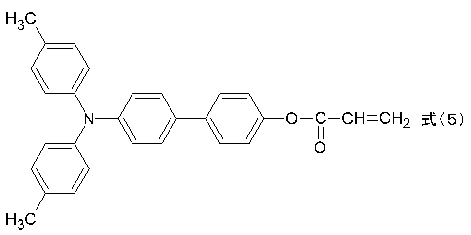
下記構造式(4)で示される化合物48.5部および例示化合物(U−1)(東京化成工業(株)製、GC純度>97%)1.5部を、n−プロパノール25部に溶解させ、さらに1,1,2,2,3,3,4−ヘプタフルオロシクロペンタン(商品名:ゼオローラH、日本ゼオン(株)製)25部を加えて、保護層用塗布液を調製した。この保護層用塗布液を上記電荷輸送層上に浸漬塗布して、これを50℃で5分間加熱処理した。その後、窒素雰囲気下にて、加速電圧150kV、吸収線量15000Gyの条件で1.5秒間電子線を照射した。さらに、窒素雰囲気下にて、130℃で90秒間加熱処理を行った。電子線の照射から30秒間の加熱処理までの酸素濃度は19ppmであった。次に、大気中において、100℃で20分間加熱処理を行い、膜厚が5μmである保護層を形成した。 48.5 parts of the compound represented by the following structural formula (4) and 1.5 parts of exemplified compound (U-1) (manufactured by Tokyo Chemical Industry Co., Ltd., GC purity> 97%) are dissolved in 25 parts of n-propanol. Further, 25 parts of 1,1,2,2,3,3,4-heptafluorocyclopentane (trade name: Zeolora H, manufactured by Nippon Zeon Co., Ltd.) was added to prepare a coating solution for a protective layer. This protective layer coating solution was dip coated on the charge transport layer, and this was heat-treated at 50 ° C. for 5 minutes. Thereafter, an electron beam was irradiated for 1.5 seconds under conditions of an acceleration voltage of 150 kV and an absorbed dose of 15000 Gy in a nitrogen atmosphere. Further, heat treatment was performed at 130 ° C. for 90 seconds in a nitrogen atmosphere. The oxygen concentration from the electron beam irradiation to the heat treatment for 30 seconds was 19 ppm. Next, heat treatment was performed at 100 ° C. for 20 minutes in the air to form a protective layer having a thickness of 5 μm.
このようにして、導電層、中間層、電荷発生層、電荷輸送層および保護層を有する電子写真感光体を製造した。 Thus, an electrophotographic photosensitive member having a conductive layer, an intermediate layer, a charge generation layer, a charge transport layer, and a protective layer was produced.
(比較例1)
実施例1において、例示化合物(U−1)を用いなかった以外は、実施例1と同様にして電子写真感光体を製造した。
(Comparative Example 1)
In Example 1, an electrophotographic photosensitive member was produced in the same manner as in Example 1 except that the exemplified compound (U-1) was not used.
(実施例2)
実施例1において、電荷輸送層用塗布液を、上記構造式(2)で示される化合物4.85部、上記構造式(3)で示される化合物4.85部、および、ポリカーボネート樹脂9.7部、例示化合物(U−1)0.6部を、モノクロロベンゼン70部およびジメトキシメタン30部の混合溶剤に溶解させて得られた電荷輸送層用塗布液に変更し、さらに比較例1で用いた保護層用塗布液に変更した以外は、実施例1と同様にして電子写真感光体を製造した。
(Example 2)
In Example 1, the charge transport layer coating solution was prepared by using 4.85 parts of the compound represented by the structural formula (2), 4.85 parts of the compound represented by the structural formula (3), and 9.7% of the polycarbonate resin. Parts of the compound (U-1) 0.6 parts in a mixed solvent of 70 parts of monochlorobenzene and 30 parts of dimethoxymethane, and then used in Comparative Example 1. An electrophotographic photosensitive member was produced in the same manner as in Example 1 except that the protective layer coating solution was changed.
(実施例3)
実施例1において、電荷輸送層用塗布液を、実施例2で用いた電荷輸送層用塗布液に変更した以外は、実施例1と同様にして電子写真感光体を製造した。
(Example 3)
An electrophotographic photosensitive member was produced in the same manner as in Example 1 except that the charge transport layer coating solution in Example 1 was changed to the charge transport layer coating solution used in Example 2.
(実施例4)
実施例1において、実施例1で用いた電荷発生層用塗布液に、さらに例示化合物(U−1)0.5部を加えて得られた電荷発生層用塗布液に変更した以外は、実施例1と同様にして電子写真感光体を製造した。
Example 4
In Example 1, except that the charge generation layer coating solution obtained in Example 1 was added to the charge generation layer coating solution obtained by adding 0.5 parts of the exemplified compound (U-1) to the charge generation layer coating solution used in Example 1. An electrophotographic photoreceptor was produced in the same manner as in Example 1.
(実施例5)
実施例1において、保護層を設けず、さらに電荷輸送層を以下の電荷輸送層に変更した以外は、実施例1と同様にして電子写真感光体を製造した。上記構造式(2)で示される化合物4.85部、上記構造式(3)で示される化合物4.85部、および、特許文献2003−195537号公報の実施例2に開示されているポリアリレート樹脂9.7部、例示化合物(U−1)0.6部を、モノクロロベンゼン57部およびジメトキシメタン30部の混合溶剤に溶解させて電荷輸送層用塗布液を得た。この電荷輸送層用塗布液を電荷発生層上に浸漬塗布し、60分間120℃で乾燥させることによって、膜厚が23μmの電荷輸送層を形成した。
(Example 5)
In Example 1, an electrophotographic photosensitive member was produced in the same manner as in Example 1 except that the protective layer was not provided and the charge transport layer was changed to the following charge transport layer. 4.85 parts of the compound represented by the structural formula (2), 4.85 parts of the compound represented by the structural formula (3), and polyarylate disclosed in Example 2 of Patent Document 2003-195537. 9.7 parts of resin and 0.6 part of exemplary compound (U-1) were dissolved in a mixed solvent of 57 parts of monochlorobenzene and 30 parts of dimethoxymethane to obtain a coating solution for charge transport layer. The charge transport layer coating solution was dip-coated on the charge generation layer and dried at 120 ° C. for 60 minutes to form a charge transport layer having a thickness of 23 μm.
(比較例2)
実施例5において、例示化合物(U−1)を用いなかった以外は、実施例5と同様にして電子写真感光体を製造した。
(Comparative Example 2)
In Example 5, an electrophotographic photosensitive member was produced in the same manner as in Example 5 except that the exemplified compound (U-1) was not used.
(実施例6)
実施例1において、保護層用塗布液を、上記構造式(4)で示される化合物を49.5部、例示化合物(U−1)を0.5部に変更して保護層用塗布液を調製した以外は、実施例1と同様にして電子写真感光体を製造した。
(Example 6)
In Example 1, the protective layer coating solution was changed to 49.5 parts of the compound represented by the above structural formula (4) and 0.5 parts of the exemplified compound (U-1). An electrophotographic photosensitive member was produced in the same manner as in Example 1 except that it was prepared.
(実施例7)
実施例1において、保護層用塗布液を、上記構造式(4)で示される化合物を47部、例示化合物(U−1)を3部に変更して保護層用塗布液を調製した以外は、実施例1と同様にして電子写真感光体を製造した。
(Example 7)
In Example 1, except that the protective layer coating liquid was prepared by changing the compound represented by the structural formula (4) to 47 parts and the exemplified compound (U-1) to 3 parts, and preparing a protective layer coating liquid. In the same manner as in Example 1, an electrophotographic photoreceptor was produced.
(実施例8)
実施例1において、保護層用塗布液を、上記構造式(4)で示される化合物を40部、例示化合物(U−1)を5部に変更して保護層用塗布液を調製した以外は、実施例1と同様にして電子写真感光体を製造した。
(Example 8)
In Example 1, except that the protective layer coating liquid was prepared by changing the compound represented by the structural formula (4) to 40 parts and the exemplified compound (U-1) to 5 parts. In the same manner as in Example 1, an electrophotographic photoreceptor was produced.
(実施例9)
実施例1において、保護層用塗布液を、上記構造式(4)で示される化合物を48.5部、例示化合物(U−1)を1.5部、およびポリテトラフルオロエチレン粒子(商品名:ルブロンL2、ダイキン(株)製)13部を、n−プロパノール25部および1,1,2,2,3,3,4−ヘプタフルオロシクロペンタン(商品名:ゼオローラH、日本ゼオン(株)製)25部の混合溶剤に加え、これを超高圧分散機で分散処理することによって得られた保護層用塗布液に変更した以外は、実施例1と同様にして電子写真感光体を製造した。
Example 9
In Example 1, 48.5 parts of the compound represented by the structural formula (4), 1.5 parts of the exemplary compound (U-1), and polytetrafluoroethylene particles (trade name) : Lubron L2, Daikin Co., Ltd. 13 parts, n-propanol 25 parts and 1,1,2,2,3,3,4-heptafluorocyclopentane (trade names: Zeolora H, Nippon Zeon Co., Ltd.) Manufactured) An electrophotographic photosensitive member was produced in the same manner as in Example 1 except that in addition to 25 parts of the mixed solvent, this was changed to a protective layer coating solution obtained by dispersing with an ultra-high pressure disperser. .
(比較例3)
実施例9において、例示化合物(U−1)を用いなかった以外は、実施例9と同様にして電子写真感光体を製造した。
(Comparative Example 3)
In Example 9, an electrophotographic photosensitive member was produced in the same manner as in Example 9 except that the exemplified compound (U-1) was not used.
(実施例10)
実施例1において、保護層用塗布液を、ジペンタエリスリトールヘキサアクリレート(商品名:DPHA、ダイセル・サイテック(株)製)(重合性官能基であるアクリル基を6つ有し、電荷輸送構造をもたない化合物)24.5部、下記構造式(5)で示される化合物24部、1−ヒドロキシ−シクロヘキシル−フェニル−ケトン(商品名:イルガキュア184、チバ・スペシャルティ・ケミカルズ製)(光重合開始剤)2.5部および例示化合物(U−1)1.5部をn−プロパノール25部に溶解させ、さらに1,1,2,2,3,3,4−ヘプタフルオロシクロペンタン25部を加えたものに変更した。そして、この保護層用塗布液を電荷輸送層上に浸漬塗布して、これを50℃で5分間加熱処理し、その後、メタルハライドランプを用いて、照射強度:500mW/cm2の条件で20秒間光照射し、130℃で30分間加熱処理を行い、膜厚が4.8μmの保護層を形成した。これ以外は、実施例1と同様にして電子写真感光体を製造した。
(Example 10)
In Example 1, the protective layer coating solution was dipentaerythritol hexaacrylate (trade name: DPHA, manufactured by Daicel-Cytec Co., Ltd.) (having six acrylic groups as polymerizable functional groups, and having a charge transport structure. No compound) 24.5 parts, 24 parts of the compound represented by the following structural formula (5), 1-hydroxy-cyclohexyl-phenyl-ketone (trade name: Irgacure 184, manufactured by Ciba Specialty Chemicals) (photopolymerization started) Agent) 2.5 parts and exemplary compound (U-1) 1.5 parts are dissolved in 25 parts of n-propanol, and 25 parts of 1,1,2,2,3,3,4-heptafluorocyclopentane is further added. Changed to what was added. Then, this protective layer coating solution is applied onto the charge transport layer by dip coating, followed by heat treatment at 50 ° C. for 5 minutes, and then using a metal halide lamp for 20 seconds under the condition of irradiation intensity: 500 mW / cm 2. The film was irradiated with light and subjected to heat treatment at 130 ° C. for 30 minutes to form a protective layer having a thickness of 4.8 μm. Except for this, an electrophotographic photoreceptor was produced in the same manner as in Example 1.
(比較例4)
実施例10において、例示化合物(U−1)を用いなかった以外は、実施例10と同様にして電子写真感光体を製造した。
(Comparative Example 4)
In Example 10, an electrophotographic photosensitive member was produced in the same manner as in Example 10 except that the exemplified compound (U-1) was not used.
(実施例11)
実施例1において、例示化合物(U−1)を例示化合物(U−25)に変更して保護層用塗布液を調製した以外は、実施例1と同様にして電子写真感光体を製造した。
(Example 11)
In Example 1, an electrophotographic photosensitive member was produced in the same manner as in Example 1 except that the exemplified compound (U-1) was changed to the exemplified compound (U-25) to prepare a protective layer coating solution.
(実施例12)
実施例1において、例示化合物(U−1)を例示化合物(U−2)に変更して保護層用塗布液を調製した以外は、実施例1と同様にして電子写真感光体を製造した。
(Example 12)
In Example 1, an electrophotographic photosensitive member was produced in the same manner as in Example 1, except that the exemplified compound (U-1) was changed to the exemplified compound (U-2) to prepare a protective layer coating solution.
(実施例13)
実施例1において、例示化合物(U−1)を例示化合物(U−26)に変更して保護層用塗布液を調製した以外は、実施例1と同様にして電子写真感光体を製造した。
(Example 13)
In Example 1, an electrophotographic photoreceptor was produced in the same manner as in Example 1 except that the exemplified compound (U-1) was changed to the exemplified compound (U-26) to prepare a protective layer coating solution.
(実施例14)
実施例1において、例示化合物(U−1)を例示化合物(U−3)に変更して保護層用塗布液を調製した以外は、実施例1と同様にして電子写真感光体を製造した。
(Example 14)
In Example 1, an electrophotographic photosensitive member was produced in the same manner as in Example 1, except that the exemplified compound (U-1) was changed to the exemplified compound (U-3) to prepare a protective layer coating solution.
(実施例15)
実施例1において、例示化合物(U−1)を例示化合物(U−4)に変更して保護層用塗布液を調製した以外は、実施例1と同様にして電子写真感光体を製造した。
(Example 15)
In Example 1, an electrophotographic photoreceptor was produced in the same manner as in Example 1 except that the exemplified compound (U-1) was changed to the exemplified compound (U-4) to prepare a protective layer coating solution.
(実施例16)
実施例1において、例示化合物(U−1)を例示化合物(U−10)に変更して保護層用塗布液を調製した以外は、実施例1と同様にして電子写真感光体を製造した。
(Example 16)
In Example 1, an electrophotographic photosensitive member was produced in the same manner as in Example 1 except that the exemplified compound (U-1) was changed to the exemplified compound (U-10) to prepare a coating solution for a protective layer.
(実施例17)
実施例1において、例示化合物(U−1)を例示化合物(U−19)に変更して保護層用塗布液を調製した以外は、実施例1と同様にして電子写真感光体を製造した。
(Example 17)
In Example 1, an electrophotographic photoreceptor was produced in the same manner as in Example 1 except that the exemplified compound (U-1) was changed to the exemplified compound (U-19) to prepare a protective layer coating solution.
(実施例18)
実施例1において、例示化合物(U−1)を例示化合物(U−24)に変更して保護層用塗布液を調製した以外は、実施例1と同様にして電子写真感光体を製造した。
(Example 18)
In Example 1, an electrophotographic photoreceptor was produced in the same manner as in Example 1 except that the exemplified compound (U-1) was changed to the exemplified compound (U-24) to prepare a protective layer coating solution.
(比較例5)
実施例1において、保護層用塗布液を、上記構造式(4)で示される化合物48.5部、ヒンダードアミン系酸化防止剤(商品名:TINUVIN622LD、チバ・ジャパン社製)0.75部、下記構造式(6)の化合物0.75部を、n−プロパノール25部に溶解させ、さらに1,1,2,2,3,3,4−ヘプタフルオロシクロペンタン25部を加えて得られた保護層用塗布液に変更した以外は、実施例1と同様にして電子写真感光体を製造した。
(Comparative Example 5)
In Example 1, 48.5 parts of the compound represented by the structural formula (4), 0.75 parts of a hindered amine antioxidant (trade name: TINUVIN622LD, manufactured by Ciba Japan), Protection obtained by dissolving 0.75 part of the compound of structural formula (6) in 25 parts of n-propanol and adding 25 parts of 1,1,2,2,3,4,4-heptafluorocyclopentane. An electrophotographic photoreceptor was produced in the same manner as in Example 1 except that the layer coating solution was changed.
(比較例6)
実施例1において、保護層用塗布液を、上記構造式(4)で示される化合物48.5部、下記構造式(7)のヒンダードアミン系酸化防止剤(商品名:サノールLS440、三共ライフテック株式会社製)1.5部を、n−プロパノール25部に溶解させ、さらに1,1,2,2,3,3,4−ヘプタフルオロシクロペンタン25部を加えて得られた保護層用塗布液に変更した以外は、実施例1と同様にして電子写真感光体を製造した。
(Comparative Example 6)
In Example 1, 48.5 parts of the compound represented by the above structural formula (4), a hindered amine antioxidant of the following structural formula (7) (trade name: Sanol LS440, Sankyo Lifetech Co., Ltd.) 1.5 parts of (manufactured by company) was dissolved in 25 parts of n-propanol, and further 25 parts of 1,1,2,2,3,3,4-heptafluorocyclopentane was added to obtain a coating solution for protective layer An electrophotographic photosensitive member was produced in the same manner as in Example 1 except that the above was changed.
(比較例7)
実施例1において、保護層用塗布液を、上記構造式(4)で示される化合物48.5部、下記構造式(8)のキノキサリン1.5部を、n−プロパノール25部に溶解させ、さらに1,1,2,2,3,3,4−ヘプタフルオロシクロペンタン25部を加えて得られた保護層用塗布液に変更した以外は、実施例1と同様にして電子写真感光体を製造した。
(Comparative Example 7)
In Example 1, 48.5 parts of the compound represented by the structural formula (4) and 1.5 parts of quinoxaline of the following structural formula (8) were dissolved in 25 parts of n-propanol. Further, an electrophotographic photosensitive member was prepared in the same manner as in Example 1 except that the protective layer coating solution was obtained by adding 25 parts of 1,1,2,2,3,3,4-heptafluorocyclopentane. Manufactured.
(比較例8)
実施例1において、保護層用塗布液を、上記構造式(4)で示される化合物48.5部、下記構造式(9)のヒンダードフェノール化合物1部(式(9)のRは、下記式(10)で示される構造を示す)、ジオクタデシル3,3′−チオジプロピオネート0.7重量部、トリス(2,4−ジ−Tert−ブチルフェニル)ホスファイト0.7重量部、1,3−ジ(4−ピリジル)プロパン0.1重量部を、n−プロパノール25部に溶解させ、さらに1,1,2,2,3,3,4−ヘプタフルオロシクロペンタン(商品名:ゼオローラH、日本ゼオン(株)製)25部を加えて得られた保護層用塗布液に変更した以外は、実施例1と同様にして電子写真感光体を製造した。
(Comparative Example 8)
In Example 1, 48.5 parts of the compound represented by the structural formula (4), 1 part of a hindered phenol compound of the following structural formula (9) (R in the formula (9) is the following: (Showing the structure represented by formula (10)), 0.7 parts by weight of dioctadecyl 3,3′-thiodipropionate, 0.7 parts by weight of tris (2,4-di-tert-butylphenyl) phosphite, 0.1 part by weight of 1,3-di (4-pyridyl) propane is dissolved in 25 parts of n-propanol, and 1,1,2,2,3,3,4-heptafluorocyclopentane (trade name: An electrophotographic photosensitive member was produced in the same manner as in Example 1 except that 25 parts of Zeorolla H (manufactured by Nippon Zeon Co., Ltd.) were added and the coating solution was changed to a protective layer coating solution.
(比較例9)
実施例1において、保護層用塗布液を、上記構造式(4)で示される化合物48.5部、下記構造式(10)で示される化合物1.5部を、n−プロパノール25部に溶解させ、さらに1,1,2,2,3,3,4−ヘプタフルオロシクロペンタン25部を加えて得られた保護層用塗布液に変更した以外は、実施例1と同様にして電子写真感光体を製造した。
(Comparative Example 9)
In Example 1, 48.5 parts of the compound represented by the structural formula (4) and 1.5 parts of the compound represented by the following structural formula (10) were dissolved in 25 parts of n-propanol. In addition, the electrophotographic photosensitive film was obtained in the same manner as in Example 1 except that the coating liquid for protective layer was changed to 25 by adding 25 parts of 1,1,2,2,3,3,4-heptafluorocyclopentane. The body was manufactured.
(比較例10〜17)
実施例1において、例示化合物(U−1)を、表1に示すように下記構造式(11)〜構造式(18)で示される化合物に変更して保護層用塗布液を調製した以外は、実施例1と同様にして電子写真感光体を製造した。
(Comparative Examples 10-17)
In Example 1, Exemplified Compound (U-1) was changed to the compounds represented by Structural Formula (11) to Structural Formula (18) as shown in Table 1 to prepare a coating solution for protective layer. In the same manner as in Example 1, an electrophotographic photoreceptor was produced.
(実施例19)
実施例1において、保護層用塗布液を、上記構造式(4)で示される化合物48.5部、例示化合物(U−1)1.5部、上記ポリテトラフルオロエチレン粒子13部、および下記式(A1)で示される繰り返し構造単位および下記式(A2)で示される繰り返し構造単位を有する樹脂(重量平均分子量130,000、(A1)/(A2)=1/1)1.5部を、n−プロパノール25部および1,1,2,2,3,3,4−ヘプタフルオロシクロペンタン25部の混合溶剤に加え、これを超高圧分散機で分散処理することによって得られた保護層用塗布液に変更した以外は、実施例1と同様にして電子写真感光体を製造した。
(Example 19)
In Example 1, the coating solution for the protective layer was prepared by using 48.5 parts of the compound represented by the structural formula (4), 1.5 parts of the exemplary compound (U-1), 13 parts of the polytetrafluoroethylene particles, and 1.5 parts of resin having a repeating structural unit represented by the formula (A1) and a repeating structural unit represented by the following formula (A2) (weight average molecular weight 130,000, (A1) / (A2) = 1/1) , 25 parts of n-propanol and 25 parts of 1,1,2,2,3,3,4-heptafluorocyclopentane, and a protective layer obtained by dispersing this with an ultrahigh pressure disperser An electrophotographic photosensitive member was produced in the same manner as in Example 1 except that the coating solution was changed to a coating solution for coating.
(比較例18)
実施例19において、例示化合物(U−1)を用いなかった以外は、実施例19と同様にして電子写真感光体を製造した。
(Comparative Example 18)
In Example 19, an electrophotographic photosensitive member was produced in the same manner as in Example 19 except that the exemplified compound (U-1) was not used.
(評価)
実施例1〜19および比較例1〜18の電子写真感光体の評価方法については、以下の通りである。
(Evaluation)
About the evaluation method of the electrophotographic photoreceptor of Examples 1-19 and Comparative Examples 1-18, it is as follows.
(黒帯の評価)
黒帯の評価を次のようにして行った。評価装置としては、キヤノン(株)製の複写機 imagePRESS C1+(コロナ帯電方式)を用いた。印字比率5%の画像において、A4サイズの普通紙にて10万枚通紙使用した。この複写機から帯電器を取り出した。
(Evaluation of black belt)
The black belt was evaluated as follows. As an evaluation apparatus, a copy machine imagePRESS C1 + (corona charging method) manufactured by Canon Inc. was used. In an image with a printing ratio of 5%, 100,000 sheets of A4 size plain paper were used. The charger was taken out from the copying machine.
もう1台別の複写機(imagePRESS C1+)を準備し、帯電器を上記の10万枚使用済みの帯電器と交換し、製造した電子写真感光体を装着した。温度23℃、湿度5%RHの環境下にて、印字比率5%の画像を、A4サイズの普通紙にて5000枚通紙使用した後、複写機への給電を停止し、15時間休止させた。15時間後に再び複写機に給電を開始し、A3サイズの普通紙、シアン単色にて、1ドット桂馬パターンのハーフトーン画像の出力を行った。ハーフトーンの濃度は、分光濃度計X−rite504(X−rite社製)にて0.85となるように光量を設定した。このハーフトーン画像について、X−Riteにて帯電器に対向していた部分と、帯電器に対向していない部分の濃度を測定した。その濃度の差を表2に示す。本発明において、濃度の差が0.1未満であれば、本発明の効果が得られていると判断した。一方、0.1以上は本発明の効果が得られていないと判断した。
Another copy machine (imagePRESS C1 +) was prepared, the charger was replaced with the above-mentioned 100,000 used charger, and the manufactured electrophotographic photosensitive member was mounted. After using 5000 sheets of A4 size plain paper for images with a printing ratio of 5% in an environment of temperature 23 ° C and
(露光部と非露光部の濃度差の評価)
露光部と非露光部の濃度差の評価を次のようにして行った。評価装置としては、キヤノン(株)の複写機 imagePRESS C1+を用いた。製造した電子写真感光体を複写機に装着した。温度23℃、湿度5%RHの環境下で、A3サイズの普通紙、シアン単色にて、2つある除電光のうち、クリーニング前露光を発光させずに、露光部と非露光部の濃度差評価用画像(図3に示すように、画像の先頭部に、白地(白画像)中に四角のベタ画像を出した後、1ドット桂馬パターンのハーフトーンを組み合わせた画像を作製。露光部と非露光部の濃度差が発生する場合、ハーフトーン部分のベタ画像からドラム1周分後に相当する部分に、ベタ画像のパターンに相当する濃度の薄い部分が生じる。)で出力した。ハーフトーンの濃度は、X−Riteにて0.85となるように光量を設定した。得られた画像のハーフトーン部分のうち、ドラム1周前が白ベタ部、黒ベタ部であった部分の濃度をX−riteで測定した。露光部と非露光部の濃度差を表2に示す。本発明において、露光部と非露光部の濃度差が−0.1よりも大きく0.0以下であれば、本発明の効果が得られていると判断した。一方、−0.1以下は本発明の効果が得られていないと判断した。
(Evaluation of density difference between exposed and unexposed areas)
The density difference between the exposed area and the non-exposed area was evaluated as follows. As an evaluation apparatus, a copy machine imagePRESS C1 + manufactured by Canon Inc. was used. The produced electrophotographic photosensitive member was mounted on a copying machine. Under the environment of temperature 23 ° C and
101 支持体
102 中間層
103 電荷発生層
104 電荷輸送層
105 保護層
1 電子写真感光体
2 軸
3 帯電手段
4 露光光
5 現像手段
6 一次転写手段
7 中間転写体
8 二次転写手段
9 転写材
10 クリーニング手段
11 前露光手段
12 前露光光
DESCRIPTION OF
Claims (4)
該電子写真装置に用いられる電子写真感光体が、支持体、支持体上に形成された電荷発生層、該電荷発生層上に形成された電荷輸送層を有し、
該電荷発生層と該電荷発生層よりも電子写真感光体表面側に位置する層のうち、少なくとも1層以上の層に、下記式(1)で示される構造を有する化合物を含有することを特徴とする電子写真装置。
(但し、
該電子写真装置がクリーニングブレードを有し、かつ、該電子写真装置が該電子写真感光体の表面と該クリーニングブレードとが当接する部位に個数平均粒径30〜500nmの塩基性粒子を供給する手段をさらに有する場合、及び、
該電子写真装置が現像手段を有し、かつ、該現像手段が個数平均粒径30〜500nmの塩基性粒子を含有する現像剤を有する場合、
を除く。)
(式(1)中、Xは、酸素原子、または硫黄原子を示す。R1およびR2は、それぞれ独立に、炭素数が1から3のアルキル基を示す。Ar1およびAr2は、それぞれ独立に、置換もしくは無置換のアリール基を示す。ただし、該アリール基が有してもよい置換基は、カルボキシル基、シアノ基、置換もしくは無置換のアミノ基、水酸基、置換もしくは無置換のアルコキシ基、置換もしくは無置換のアルキル基、ニトロ基、または、ハロゲン原子である。) In an electrophotographic apparatus having a charging means for charging an electrophotographic photosensitive member by a charging method involving discharge,
The electrophotographic photosensitive member used in the electrophotographic apparatus has a support, a charge generation layer formed on the support, a charge transport layer formed on the charge generation layer,
Among the charge generation layer and the layer located on the surface side of the electrophotographic photoreceptor from the charge generation layer, at least one layer contains a compound having a structure represented by the following formula (1) An electrophotographic apparatus.
(However,
The electrophotographic apparatus has a cleaning blade, and the electrophotographic apparatus supplies basic particles having a number average particle size of 30 to 500 nm to a portion where the surface of the electrophotographic photosensitive member is in contact with the cleaning blade. And
When the electrophotographic apparatus has a developing means, and the developing means has a developer containing basic particles having a number average particle size of 30 to 500 nm,
except for. )
(In formula (1), X represents an oxygen atom or a sulfur atom. R 1 and R 2 each independently represents an alkyl group having 1 to 3 carbon atoms. Ar 1 and Ar 2 are each represented by Independently, it represents a substituted or unsubstituted aryl group, provided that the aryl group may have a carboxyl group, a cyano group, a substituted or unsubstituted amino group, a hydroxyl group, a substituted or unsubstituted alkoxy group. Group, substituted or unsubstituted alkyl group, nitro group, or halogen atom.)
前記電荷輸送層、および該保護層の少なくとも一方の層が前記式(1)で示される構造を有する化合物を含有する請求項1に記載の電子写真装置。 The electrophotographic photoreceptor has a protective layer formed on the charge transport layer,
The electrophotographic apparatus according to claim 1, wherein at least one of the charge transport layer and the protective layer contains a compound having a structure represented by the formula (1).
Priority Applications (1)
| Application Number | Priority Date | Filing Date | Title |
|---|---|---|---|
| JP2011023858A JP5725890B2 (en) | 2011-02-07 | 2011-02-07 | Electrophotographic equipment |
Applications Claiming Priority (1)
| Application Number | Priority Date | Filing Date | Title |
|---|---|---|---|
| JP2011023858A JP5725890B2 (en) | 2011-02-07 | 2011-02-07 | Electrophotographic equipment |
Publications (3)
| Publication Number | Publication Date |
|---|---|
| JP2012163758A JP2012163758A (en) | 2012-08-30 |
| JP2012163758A5 JP2012163758A5 (en) | 2014-03-27 |
| JP5725890B2 true JP5725890B2 (en) | 2015-05-27 |
Family
ID=46843197
Family Applications (1)
| Application Number | Title | Priority Date | Filing Date |
|---|---|---|---|
| JP2011023858A Active JP5725890B2 (en) | 2011-02-07 | 2011-02-07 | Electrophotographic equipment |
Country Status (1)
| Country | Link |
|---|---|
| JP (1) | JP5725890B2 (en) |
Families Citing this family (3)
| Publication number | Priority date | Publication date | Assignee | Title |
|---|---|---|---|---|
| JP6242152B2 (en) * | 2012-11-19 | 2017-12-06 | キヤノン株式会社 | Electrophotographic photosensitive member, method for manufacturing electrophotographic photosensitive member, process cartridge, and electrophotographic apparatus |
| JP6242151B2 (en) * | 2012-11-19 | 2017-12-06 | キヤノン株式会社 | Electrophotographic photosensitive member, method for manufacturing electrophotographic photosensitive member, process cartridge, and electrophotographic apparatus |
| JP6815758B2 (en) | 2016-06-15 | 2021-01-20 | キヤノン株式会社 | Electrophotographic photosensitive member, manufacturing method of electrophotographic photosensitive member, electrophotographic apparatus and process cartridge having the electrophotographic photosensitive member. |
Family Cites Families (8)
| Publication number | Priority date | Publication date | Assignee | Title |
|---|---|---|---|---|
| JPS5865438A (en) * | 1981-10-15 | 1983-04-19 | Fuji Photo Film Co Ltd | Photoconductive conposition and electrophotographic sensitive material using it |
| JPS5865439A (en) * | 1981-10-15 | 1983-04-19 | Fuji Photo Film Co Ltd | Photoconductive composition and electrophotographic sensitive material using it |
| JPS6397959A (en) * | 1986-10-14 | 1988-04-28 | Konica Corp | Electrophotographic sensitive body |
| JP2687235B2 (en) * | 1989-03-03 | 1997-12-08 | 富士写真フイルム株式会社 | Electrophotographic photoreceptor |
| JPH04100052A (en) * | 1990-08-20 | 1992-04-02 | Dainippon Ink & Chem Inc | Electrophotographic printing plate |
| JPH07128891A (en) * | 1993-09-07 | 1995-05-19 | Nippon Paint Co Ltd | Photosensitive resin composition for printing and resin plate for printing |
| JPH07140693A (en) * | 1993-11-18 | 1995-06-02 | Ricoh Co Ltd | Electrophotographic photoreceptor |
| JP5258410B2 (en) * | 2008-06-20 | 2013-08-07 | キヤノン株式会社 | Electrophotographic photosensitive member, process cartridge, and electrophotographic apparatus |
-
2011
- 2011-02-07 JP JP2011023858A patent/JP5725890B2/en active Active
Also Published As
| Publication number | Publication date |
|---|---|
| JP2012163758A (en) | 2012-08-30 |
Similar Documents
| Publication | Publication Date | Title |
|---|---|---|
| KR101548788B1 (en) | Electrophotographic photosensitive member, process cartridge, and electrophotographic apparatus | |
| JP6429498B2 (en) | Electrophotographic photosensitive member, method for manufacturing electrophotographic photosensitive member, process cartridge, and electrophotographic apparatus | |
| JP2019035804A (en) | Electrophotographic photosensitive member, production method of electrophotographic photosensitive member, process cartridge, and electrophotographic apparatus | |
| JP5680015B2 (en) | Electrophotographic photosensitive member, process cartridge, and electrophotographic apparatus | |
| JP5857827B2 (en) | Electrophotographic photosensitive member, process cartridge, and image forming apparatus | |
| EP2600200A1 (en) | Electrophotographic photosensitive member, method of producing electrophotographic photosensitive member, process cartridge, and electrophotographic apparatus | |
| JP3384231B2 (en) | Electrophotographic photosensitive member and image forming apparatus using the same | |
| JP5725890B2 (en) | Electrophotographic equipment | |
| JP2005062301A (en) | Electrophotographic photoreceptor | |
| JP2005062300A (en) | Electrophotographic photoreceptor, process cartridge, and electrophotographic apparatus | |
| JP6071733B2 (en) | Electrophotographic photosensitive member, method for manufacturing electrophotographic photosensitive member, process cartridge, and electrophotographic apparatus | |
| JP6226714B2 (en) | Electrophotographic photosensitive member, method for manufacturing electrophotographic photosensitive member, process cartridge, and electrophotographic apparatus | |
| JP2007147824A (en) | Electrophotographic photoreceptor and image forming apparatus | |
| JP2003186222A (en) | Electrophotographic photoreceptor, and process cartridge and electrophotographic device having the electrophotographic photoreceptor | |
| JP6327981B2 (en) | Electrophotographic photosensitive member, process cartridge, and electrophotographic apparatus | |
| JP2007163578A (en) | Electrophotographic photoreceptor, process cartridge and electrophotographic apparatus | |
| JP2005202022A (en) | Electrophotographic photoreceptor and image forming apparatus provided with the same | |
| US8859172B2 (en) | Electrophotographic photosensitive member, method of producing electrophotographic photosensitive member, process cartridge, and electrophotographic apparatus | |
| JP2015184342A (en) | Electrophotographic device and process cartridge | |
| JP6391400B2 (en) | Electrophotographic photosensitive member, method for manufacturing electrophotographic photosensitive member, process cartridge, and electrophotographic apparatus | |
| JP5625602B2 (en) | Electrophotographic photosensitive member, and electrophotographic forming method, electrophotographic forming apparatus and process cartridge using the same | |
| JP5718413B2 (en) | Electrophotographic photosensitive member and image forming apparatus using the same | |
| JP3367318B2 (en) | Electrophotographic photosensitive member and image forming apparatus using the same | |
| JP2018017887A (en) | Electrophotographic photoreceptor, method for manufacturing electrophotographic photoreceptor, process cartridge, electrophotographic device and method for extracting filling member | |
| JP2005055729A (en) | Electrophotographic photoreceptor, method for manufacturing the same, process cartridge and electrophotographic apparatus |
Legal Events
| Date | Code | Title | Description |
|---|---|---|---|
| A521 | Written amendment |
Free format text: JAPANESE INTERMEDIATE CODE: A523 Effective date: 20140205 |
|
| A621 | Written request for application examination |
Free format text: JAPANESE INTERMEDIATE CODE: A621 Effective date: 20140205 |
|
| A977 | Report on retrieval |
Free format text: JAPANESE INTERMEDIATE CODE: A971007 Effective date: 20141021 |
|
| A131 | Notification of reasons for refusal |
Free format text: JAPANESE INTERMEDIATE CODE: A132 Effective date: 20141028 |
|
| A521 | Written amendment |
Free format text: JAPANESE INTERMEDIATE CODE: A523 Effective date: 20150105 |
|
| TRDD | Decision of grant or rejection written | ||
| A01 | Written decision to grant a patent or to grant a registration (utility model) |
Free format text: JAPANESE INTERMEDIATE CODE: A01 Effective date: 20150303 |
|
| A61 | First payment of annual fees (during grant procedure) |
Free format text: JAPANESE INTERMEDIATE CODE: A61 Effective date: 20150331 |
|
| R151 | Written notification of patent or utility model registration |
Ref document number: 5725890 Country of ref document: JP Free format text: JAPANESE INTERMEDIATE CODE: R151 |