JP5716601B2 - Insulation resistance drop detector - Google Patents
Insulation resistance drop detector Download PDFInfo
- Publication number
- JP5716601B2 JP5716601B2 JP2011169280A JP2011169280A JP5716601B2 JP 5716601 B2 JP5716601 B2 JP 5716601B2 JP 2011169280 A JP2011169280 A JP 2011169280A JP 2011169280 A JP2011169280 A JP 2011169280A JP 5716601 B2 JP5716601 B2 JP 5716601B2
- Authority
- JP
- Japan
- Prior art keywords
- voltage
- insulation resistance
- resistance
- circuit
- amplitude
- Prior art date
- Legal status (The legal status is an assumption and is not a legal conclusion. Google has not performed a legal analysis and makes no representation as to the accuracy of the status listed.)
- Active
Links
Images


Classifications
-
- H—ELECTRICITY
- H02—GENERATION; CONVERSION OR DISTRIBUTION OF ELECTRIC POWER
- H02H—EMERGENCY PROTECTIVE CIRCUIT ARRANGEMENTS
- H02H3/00—Emergency protective circuit arrangements for automatic disconnection directly responsive to an undesired change from normal electric working condition with or without subsequent reconnection ; integrated protection
- H02H3/16—Emergency protective circuit arrangements for automatic disconnection directly responsive to an undesired change from normal electric working condition with or without subsequent reconnection ; integrated protection responsive to fault current to earth, frame or mass
- H02H3/17—Emergency protective circuit arrangements for automatic disconnection directly responsive to an undesired change from normal electric working condition with or without subsequent reconnection ; integrated protection responsive to fault current to earth, frame or mass by means of an auxiliary voltage injected into the installation to be protected
-
- H—ELECTRICITY
- H02—GENERATION; CONVERSION OR DISTRIBUTION OF ELECTRIC POWER
- H02H—EMERGENCY PROTECTIVE CIRCUIT ARRANGEMENTS
- H02H3/00—Emergency protective circuit arrangements for automatic disconnection directly responsive to an undesired change from normal electric working condition with or without subsequent reconnection ; integrated protection
- H02H3/02—Details
- H02H3/04—Details with warning or supervision in addition to disconnection, e.g. for indicating that protective apparatus has functioned
- H02H3/044—Checking correct functioning of protective arrangements, e.g. by simulating a fault
Landscapes
- Engineering & Computer Science (AREA)
- Power Engineering (AREA)
- Testing Of Short-Circuits, Discontinuities, Leakage, Or Incorrect Line Connections (AREA)
- Emergency Protection Circuit Devices (AREA)
- Electric Propulsion And Braking For Vehicles (AREA)
Description
この発明は、絶縁抵抗低下検出装置に関し、特に、蓄電装置と蓄電装置の電圧を変換する電圧コンバータとを備えた電源装置の絶縁抵抗の低下を検出する絶縁抵抗低下検出装置に関する。 The present invention relates to an insulation resistance decrease detection device, and more particularly to an insulation resistance decrease detection device that detects a decrease in insulation resistance of a power supply device including a power storage device and a voltage converter that converts the voltage of the power storage device.
高電圧を使用する装置では、動作中の絶縁抵抗を正確に検出することが漏電防止に重要である。このような高電圧を使用する装置は、電源装置の絶縁抵抗を正確に検出する検出装置を備えている。たとえば、ハイブリッドカーや電気自動車等の電動車両では、モータを駆動する電源装置の絶縁抵抗を正確に検出する検出装置を備えている。 In a device that uses a high voltage, it is important to accurately detect the insulation resistance during operation to prevent leakage. A device using such a high voltage includes a detection device that accurately detects the insulation resistance of the power supply device. For example, an electric vehicle such as a hybrid car or an electric vehicle includes a detection device that accurately detects an insulation resistance of a power supply device that drives a motor.
特開2004−354247号公報(特許文献1)は、擬似漏電状態を作り、擬似漏電状態で漏電が検出されないと検出異常であると判断することで、漏電検出器の自己診断を行なう技術が開示されている。 Japanese Patent Application Laid-Open No. 2004-354247 (Patent Document 1) discloses a technique for performing a self-diagnosis of a leakage detector by creating a pseudo-leakage state and determining that a leakage is not detected in the pseudo-leakage state when the leakage is not detected. Has been.
上記特開2004−354247号公報に記載された技術では、自己診断時にしか使用しない擬似漏電状態を作るための専用回路が必要であり、コストおよび回路実装面積の点で不利である。 The technique described in Japanese Patent Application Laid-Open No. 2004-354247 requires a dedicated circuit for creating a pseudo-leakage state that is used only during self-diagnosis, which is disadvantageous in terms of cost and circuit mounting area.
この発明の目的は、コストおよび回路実装面積が改善された自己診断可能な絶縁抵抗低下検出装置を提供することである。 An object of the present invention is to provide a self-diagnosis insulation resistance drop detecting device with improved cost and circuit mounting area.
この発明は、要約すると、蓄電装置と蓄電装置の電圧を変換する電圧コンバータとを備えた電源装置の絶縁抵抗の低下を検出する絶縁抵抗低下検出装置であって、筐体と蓄電装置によって電源が供給される部分との間の絶縁抵抗を検出する抵抗検出部と、抵抗検出部の自己診断のための制御を行なう制御装置とを備える。制御装置は、自己診断を実行する際に電圧コンバータに対して電圧変動を発生させ、電圧変動の有無に対する抵抗検出部の検出結果の変化に基づいて抵抗検出部の自己診断を実行する。 In summary, the present invention provides an insulation resistance lowering detection device that detects a decrease in insulation resistance of a power supply device that includes a power storage device and a voltage converter that converts the voltage of the power storage device. A resistance detection unit that detects an insulation resistance between the supplied portion and a control device that performs control for self-diagnosis of the resistance detection unit. When executing the self-diagnosis, the control device generates a voltage fluctuation in the voltage converter, and executes the self-diagnosis of the resistance detection unit based on the change in the detection result of the resistance detection unit with respect to the presence or absence of the voltage fluctuation.
好ましくは、制御装置は、電圧コンバータの出力電圧に電圧変動として蓄電装置の電圧よりも高い電圧を中心とする所定振幅、所定周期の正弦波が発生するように、電圧コンバータを制御する。 Preferably, the control device controls the voltage converter such that a sine wave having a predetermined amplitude and a predetermined cycle centered on a voltage higher than the voltage of the power storage device is generated as a voltage fluctuation in the output voltage of the voltage converter.
より好ましくは、抵抗検出部は、絶縁抵抗に一方端が接続されるカップリングコンデンサと、カップリングコンデンサの他方端に検出抵抗を介して接続される発振回路と、カップリングコンデンサの他方端の電圧波形の振幅に基づいて絶縁抵抗の低下の有無を判定する判定回路とを含む。 More preferably, the resistance detection unit includes a coupling capacitor having one end connected to the insulation resistor, an oscillation circuit connected to the other end of the coupling capacitor via the detection resistor, and a voltage at the other end of the coupling capacitor. And a determination circuit that determines the presence or absence of a decrease in insulation resistance based on the amplitude of the waveform.
さらに好ましくは、正弦波の振幅は、発振回路の出力する信号の振幅よりも大きい。
さらに好ましくは、判定回路は、発振回路の出力信号を通過させるバンドパスフィルタを含む。制御装置は、電圧コンバータに対してバンドパスフィルタの通過帯域の周波数に対応する電圧変動を電圧コンバータに対して発生させる。
More preferably, the amplitude of the sine wave is larger than the amplitude of the signal output from the oscillation circuit.
More preferably, the determination circuit includes a band pass filter that passes the output signal of the oscillation circuit. The control device causes the voltage converter to generate a voltage fluctuation corresponding to the frequency of the pass band of the bandpass filter.
好ましくは、蓄電装置および電圧コンバータは車両に搭載される。筐体は車両のボディである。 Preferably, the power storage device and the voltage converter are mounted on a vehicle. The housing is the vehicle body.
本発明によれば、擬似漏電状態を作るための専用の回路を必要としないので、コストを低減させ、回路実装面積を小さくすることが可能となる。 According to the present invention, since a dedicated circuit for creating a pseudo-leakage state is not required, the cost can be reduced and the circuit mounting area can be reduced.
本発明の実施の形態について図面を参照しながら詳細に説明する。なお、図中同一または相当部分には同一符号を付してその説明は繰返さない。 Embodiments of the present invention will be described in detail with reference to the drawings. In the drawings, the same or corresponding parts are denoted by the same reference numerals and description thereof will not be repeated.
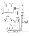
図1は、本実施の形態による車両の構成を示す回路図である。図1に示す車両100は、高圧バッテリを搭載するものであれば、電気自動車でもハイブリッド自動車でも燃料電池自動車でもよい。
FIG. 1 is a circuit diagram showing a configuration of a vehicle according to the present embodiment. The
図1を参照して、車両100は、共に直流電源の一種である高圧バッテリB1と、システムメインリレーSR1,SR2と、電圧センサ10,13,16と、電圧コンバータ11と、正極母線PLと、負極母線NLと、コンデンサ12,14と、電流センサ17と、インバータ20と、モータジェネレータMG1,MG2と、制御装置30と、絶縁抵抗検出部70とを含む。
Referring to FIG. 1,
電圧コンバータ11は、リアクトルL1と、IGBT素子Q1,Q2と、ダイオードD1,D2とを含む。リアクトルL1は、その一方端が高圧バッテリB1の正極に接続され、他方端がIGBT素子Q1のエミッタとIGBT素子Q2のコレクタの接続ノードに接続される。
IGBT素子Q1,Q2は、正極母線PLと負極母線NLとの間に直列に接続される。IGBT素子Q1は、コレクタが正極母線PLに接続され、エミッタがIGBT素子Q2のコレクタに接続される。IGBT素子Q2は、エミッタが負極母線NLに接続される。 IGBT elements Q1, Q2 are connected in series between positive electrode bus PL and negative electrode bus NL. IGBT element Q1 has a collector connected to positive electrode bus PL and an emitter connected to the collector of IGBT element Q2. IGBT element Q2 has an emitter connected to negative electrode bus NL.
また、各IGBT素子Q1,Q2のコレクタ−エミッタ間には、エミッタ側からコレクタ側へ電流を流すダイオードD1,D2がそれぞれ接続されている。 Further, diodes D1 and D2 for passing a current from the emitter side to the collector side are connected between the collector and emitter of the IGBT elements Q1 and Q2, respectively.
モータジェネレータMG1,MG2は、3相の永久磁石モータであり、U,V,W相コイルを含む。インバータ20は、モータジェネレータMG1,MG2を駆動する。
Motor generators MG1 and MG2 are three-phase permanent magnet motors, and include U, V, and W phase coils.
絶縁抵抗検出部70は、カップリングコンデンサ15と、発振回路40と、抵抗50と、インピーダンス判定回路60とを含む。カップリングコンデンサ15は、高圧バッテリB1の負極端子とノードN1との間に接続される。抵抗50は、ノードN1と発振回路40との間に接続される。
高圧バッテリB1は、ニッケル水素電池あるいはリチウムイオン電池等の二次電池または電気二重層コンデンサ等の蓄電素子を含んで構成することができる。そして、高圧バッテリB1は、直流電圧VBをシステムメインリレーSR1,SR2を介して電圧コンバータ11へ供給する。
The high voltage battery B1 can include a secondary battery such as a nickel metal hydride battery or a lithium ion battery, or a power storage element such as an electric double layer capacitor. High voltage battery B1 supplies DC voltage VB to
システムメインリレーSR1,SR2は、制御装置30からの信号SEによってオン/オフされる。より具体的には、システムメインリレーSR1,SR2は、制御装置30からのH(論理ハイ)レベルの信号SEによりオンされ、制御装置30からのL(論理ロー)レベルの信号SEによりオフされる。
System main relays SR1 and SR2 are turned on / off by signal SE from
電圧センサ10は、高圧バッテリB1から出力される直流電圧VBを検出し、直流電圧VBの検出値を制御装置30へ出力する。
電圧センサ13は、電圧コンバータ11の高圧バッテリB1側の入力に与えられる直流電圧VLを検出し、直流電圧VLの検出値を制御装置30へ出力する。
電流センサ17は、高圧バッテリB1に入出力する直流電流BCRTを検出し、直流電流BCRTの検出値を制御装置30へ出力する。
電圧コンバータ11は、制御装置30からの信号PWMUに基づいて、高圧バッテリB1からの直流電圧VHを昇圧してコンデンサ12に供給する。また、電圧コンバータ11は、制御装置30からの信号PWMDまたはPWMLに基づいて、インバータ20から供給された直流電圧を降圧して高圧バッテリB1へ供給する。
The
コンデンサ12は、電圧コンバータ11から供給された直流電圧を平滑化してインバータ20に供給する。コンデンサ14は、電圧コンバータ11の高圧バッテリB1側の入力に与えられる直流電圧VLを平滑化する。
電圧センサ16は、コンデンサ12の両端の電圧VHを検出し、その検出した電圧VHを制御装置30へ出力する。
The
インバータ20は、制御装置30からの信号PWMIに基づいて、コンデンサ12を介して電圧コンバータ11から供給された直流電圧を交流電圧に変換してモータジェネレータMG1およびMG2を駆動する。また、インバータ20は、制御装置30からの信号PWMCに基づいて、モータジェネレータMG1およびMG2が発電した交流電圧を直流電圧に変換し、その変換した直流電圧をコンデンサ12を介して電圧コンバータ11へ供給する。
制御装置30は、電圧センサ10からの直流電圧VB、電圧センサ16からの電圧VH、車両100の外部に設けられたECU(Electrical Control Unit)からのモータ回転数MRNおよびトルク指令値TRに基づいて、信号PWMUまたは信号PWMDを生成し、その生成した信号PWMUまたは信号PWMDを電圧コンバータ11へ出力する。
さらに、制御装置30は、電圧センサ16からの電圧VH、図示しない電流センサで検出されたモータ電流値および外部ECUからのトルク指令値TRに基づいて、信号PWMIまたは信号PWMCを生成し、その生成した信号PWMIまたは信号PWMCをインバータ20へ出力する。
Further,
発振回路40は、所定周波数の交流信号Eoを発振し、その発振した交流信号Eoを抵抗50を介してノードN1へ出力する。インピーダンス判定回路60は、ノードN1から交流信号Eを受け、その受けた交流信号Eの波高値を検出する。
The
高圧システムからの漏電経路は、抵抗成分Riで示すような、高圧バッテリB1や負極母線NLのような直流部からシャーシグラウンドGND(ボデーGNDとも称する)への漏電経路が考えられる。 The leakage path from the high voltage system may be a leakage path from a direct current section such as the high voltage battery B1 or the negative electrode bus NL to the chassis ground GND (also referred to as body GND) as indicated by the resistance component Ri.
直流部については、車両が起動されると、システムメインリレーSR1,SR2を導通させる前に絶縁劣化の有無を判定し、さらにシステムメインリレーSR1,SR2を導通させた後にも負極母線NLの絶縁劣化の有無を繰り返し判定している。 As for the direct current section, when the vehicle is started, it is determined whether or not insulation deterioration has occurred before the system main relays SR1 and SR2 are turned on. Further, even after the system main relays SR1 and SR2 are turned on, the insulation deterioration of the negative electrode bus NL is determined. The presence or absence of is repeatedly determined.
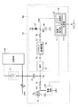
図2は、図1の絶縁抵抗検出部70のより詳細な構成を示した回路図である。
図2を参照して、回路系200は図1に示す車両システムの高圧回路系を1つの機能ブロックにより示したものである。また、図2に示す接地ノードは車両においてはボデーアース(車体)に対応する。
FIG. 2 is a circuit diagram showing a more detailed configuration of the
Referring to FIG. 2, a
絶縁抵抗検出部70は、信号発生部である発振回路40と、絶縁劣化検出用の抵抗50と、カップリングコンデンサ15と、インピーダンス判定回路60とを含む。インピーダンス判定回路60は、バンドパスフィルタ(BPF)84と、オフセット回路および増幅回路からなる回路ブロック85と、過電圧保護用ダイオード87と、抵抗86と、コンデンサ88と、制御回路110とを含む。
発振回路40は、ノードNAに所定周波数(所定周期Tp)で変化するパルス信号SIGを印加する。抵抗50は、ノードNAおよびノードN1の間に接続される。カップリングコンデンサ15は、絶縁劣化検出対象となる高圧バッテリB1とノードN1との間に接続される。バンドパスフィルタ84は、ノードN1に入力端子が接続され、ノードN2に出力端子が接続される。バンドパスフィルタ84の通過帯域周波数は、パルス信号SIGの周波数に合わせて設計される。
The
回路ブロック85は、ノードN2とノードN3との間に接続される。回路ブロック85は、バンドパスフィルタ84を通過したパルス信号のうち、絶縁抵抗検出時に設定されるしきい値電圧付近の電圧変化を増幅する。過電圧保護用ダイオード87は、電源ノードにカソードが接続され、ノードNBにアノードが接続されて、サージ電圧(高電圧,負電圧)を除去する。抵抗86はノードN3とノードNBとの間に接続される。コンデンサ88はノードNBと接地ノードとの間に接続される。抵抗86およびコンデンサ88は、回路ブロック85から出力される信号のノイズを除去するフィルタとして機能する。
The
制御回路110は、発振回路40を制御する。また制御回路110は、ノードNBの電圧を検出して、検出電圧Vrefに基づいて絶縁抵抗Riの低下を検出する。制御回路110は、発振指令部111と、A/D変換部112と、判定部113とを含む。
The
発振指令部111は、発振回路40に対してパルス信号SIGを発生するよう指示を与えるとともに、パルス信号SIGのデューティ比を変更するよう指示する。A/D変換部112は所定のサンプリング周期Tsにより検出したノードNBの電圧(検出電圧)をA/D変換する。サンプリング周期Tsはパルス信号SIGの周期Tpよりも十分短いのでノードNBの最大電圧(ピーク電圧Vp)および最小電圧を検出できる。判定部113は、A/D変換部112から取得したピーク電圧Vpの値と、しきい値とを比較する。これにより、制御回路110は、絶縁抵抗Riの低下の有無を検出する。
The oscillation command unit 111 instructs the
次に、絶縁抵抗Riの低下を検出する動作について説明する。発振回路40によって発生されたパルス信号SIGは、抵抗50、カップリングコンデンサ15、絶縁抵抗Ri、およびバンドパスフィルタ84を含んで構成された直列回路に印加される。これにより、抵抗50およびカップリングコンデンサ15の接続点に相当するノードN1には、絶縁抵抗Riおよび抵抗50(抵抗値Rd)の分圧比:Ri/(Rd+Ri)とパルス信号SIGの振幅(電源電圧である電圧+B)との積に関連する値を波高値とするパルス電圧が発生する。なお電圧+Bは、たとえば補機バッテリの電圧としてもよいが、これに限定されるものではない。
Next, an operation for detecting a decrease in the insulation resistance Ri will be described. The pulse signal SIG generated by the
ノードN1に発生したパルス電圧は、バンドパスフィルタ84によってパルス信号SIGの周波数以外の成分が減衰される。バンドパスフィルタ84を通過したパルス信号SIGのうち、しきい値電圧付近の電圧変化のみが回路ブロック85によって増幅される。回路ブロック85から出力される信号はノードNBに伝達される。ノードN3からノードNBに信号が伝達されるに際して、過電圧保護用ダイオード87によりサージ電圧が除去されるとともに、抵抗86およびコンデンサ88によってノイズが除去される。
In the pulse voltage generated at the node N1, components other than the frequency of the pulse signal SIG are attenuated by the band-
絶縁抵抗Riが正常である時には、Ri>>Rdである。Riが高くなるに従って、ピーク電圧Vpは電圧+Bにほぼ等しくなる。一方、絶縁抵抗Riの低下時には、分圧比:Ri/(Rd+Ri)が低下するので、ピーク電圧Vpが低下する。ピーク電圧Vpの低下を検出することにより、絶縁劣化の発生を検出することができる。そして、検出抵抗値Rdは固定値であるので、ピーク電圧Vpを観測すれば、絶縁抵抗Riの値を算出することも可能である。 When the insulation resistance Ri is normal, Ri >> Rd. As Ri increases, the peak voltage Vp becomes substantially equal to the voltage + B. On the other hand, when the insulation resistance Ri is lowered, the voltage division ratio: Ri / (Rd + Ri) is lowered, so that the peak voltage Vp is lowered. By detecting a decrease in the peak voltage Vp, the occurrence of insulation deterioration can be detected. Since the detection resistance value Rd is a fixed value, the value of the insulation resistance Ri can be calculated by observing the peak voltage Vp.
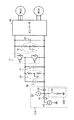
図3は、高圧系の絶縁抵抗の低下を検出する簡易モデルを示した回路図である。
図3を参照して、絶縁抵抗低下検出器201は、アース203を基準電位として振幅V0で発振波形を出力する発振電源204と、発振電源204から一方端に発振信号を受ける検出抵抗206と、検出抵抗206の他方端に一方電極が接続されたカップリングコンデンサ210とを含む。
FIG. 3 is a circuit diagram showing a simple model for detecting a decrease in insulation resistance of a high voltage system.
Referring to FIG. 3, an insulation
高圧簡易モデル202は、カップリングコンデンサ210の他方電極とアース216との間に並列に接続された高圧絶縁抵抗212およびコモンモードコンデンサ214を含む。
High-voltage
高電圧バッテリや駆動回路は、高圧簡易モデル202のように表すことができる。高圧簡易モデル202のインピーダンスが大きい場合には、検出抵抗206(抵抗値Rd)にはほとんど電流が流れない。したがって電圧検出器208が検出する電圧波形は発振電源204の信号振幅電圧V0と同じ振幅となる(Vd=V0)。
The high voltage battery and the drive circuit can be expressed as a high voltage
高圧簡易モデル202のインピーダンスが小さいときには、検出抵抗206に電流が流れるため、その分振幅が電圧ドロップした波形が電圧検出器208によって計測でき、これによって異常が判定できる。
When the impedance of the high-voltage
図4は、検討例である車両の構成を示す回路図である。
図4に示した車両は、図1に示した車両100の構成において、絶縁抵抗検出部70に代えて絶縁抵抗検出部70Aを含む。他の部分の構成は、図1に示した車両100と基本的には同様であるので説明は繰返さない。なお、電圧センサ13,16は、絶縁抵抗に着目して簡略化した等価回路で示すと図4に示すように正負極母線間に直列接続された抵抗で表現され、それらの抵抗の接続点は車両のボデーに結合されている。図1に示した車両100の電圧センサ13,16にもこの等価回路は共通する。電圧センサ13,16には、差動式電圧検出回路が使用されており、正極母線と負極母線の中間がボデーGNDの電位となる。
FIG. 4 is a circuit diagram illustrating a configuration of a vehicle which is an example of examination.
The vehicle shown in FIG. 4 includes an insulation
絶縁抵抗検出部70Aは、カップリングコンデンサ15と、発振回路40と、抵抗50と、インピーダンス判定回路60とを含む。カップリングコンデンサ15は、高圧バッテリB1の負極端子とノードN1との間に接続される。抵抗50は、ノードN1と発振回路40との間に接続される。
絶縁抵抗検出部70Aは、さらに、自己診断用の専用回路300を含む。専用回路300は、ノードN1とボデーGNDとの間に直列に接続されたスイッチと抵抗とを含む。
この検討例では、車両起動後(IGON後)経過時間が5〜40秒の時に専用回路300内部のスイッチを導通させて、ノードN1が擬似的に絶縁低下した状態を作る。この状態では、インピーダンス判定回路60に入力される検出信号が絶縁低下時と同じ状態となる。
In this examination example, when the elapsed time after starting the vehicle (after IGON) is 5 to 40 seconds, the switch in the
この状態でインピーダンス判定回路60が絶縁低下時と同じ検出結果を示せば、絶縁抵抗検出部70Aが正常であると自己診断される。一方、この状態でインピーダンス判定回路60が絶縁正常時と同じ検出結果を示せば、絶縁抵抗検出部70Aが異常であると自己診断される。
In this state, if the
しかし、このような自己診断用の専用回路300を搭載するのは、部品点数増加の点からコスト増を招く。また実装面積増加から装置の大きさが大きくなる。
However, mounting such a
したがって、図1に示した本実施の形態の車両では、絶縁抵抗検出部70にこのような自己診断用の専用回路300は搭載していない。その代わりに、自己診断時に電圧コンバータ11の出力する直流電圧VHを意図的に変動させることによってノードN1の電圧を絶縁低下時と同様に変化させる。
Therefore, in the vehicle of the present embodiment shown in FIG. 1, such a
図5は、図1の制御装置30が実行する自己診断に関する処理を説明するためのフローチャートである。
FIG. 5 is a flowchart for explaining processing relating to self-diagnosis executed by the
図1、図5を参照して、まず処理が開始されるとステップS1において、漏電検出器(絶縁抵抗検出部70)の自己診断実施が許可されているか否かが判断される。たとえば、車両起動信号IGONが入力されてから5秒以上経過かつ40秒以内であるときに、自己診断を許可するようにすることができる。なお、この許可条件は自己診断に都合の良いタイミングであれば、これに限定されずどのようなタイミングでも良い。たとえば、車両停止信号が入力された場合に自己診断を行なってから車両のシステムを停止させるようにしても良い。 Referring to FIGS. 1 and 5, when the process is started, it is determined in step S1 whether or not self-diagnosis of the leakage detector (insulation resistance detector 70) is permitted. For example, the self-diagnosis can be permitted when 5 seconds or more have passed since the vehicle activation signal IGON was input and within 40 seconds. The permission condition is not limited to this as long as it is convenient for self-diagnosis, and any timing may be used. For example, the vehicle system may be stopped after a self-diagnosis is performed when a vehicle stop signal is input.
ステップS1において、自己診断実施が許可されていない場合には、ステップS1に処理が戻る一方で、自己診断実施が許可されていた場合には、ステップS2に処理が進む。 If the execution of self-diagnosis is not permitted in step S1, the process returns to step S1. If the execution of self-diagnosis is permitted, the process proceeds to step S2.
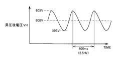
ステップS2では、制御装置30は、電圧コンバータ11に昇圧後電圧(直流電圧VH)を電池電圧VBよりも高い電圧(たとえばVB+10V)を中心にして所定振幅(例えば10V)かつ所定周波数(たとえば2.5Hz)の正弦波となるように昇圧制御を実施する。
In step S2,
図6は、図5のステップS2の処理が実行された結果の直流電圧VHの変動の一例の様子を示した図である。 FIG. 6 is a diagram showing an example of the variation of the DC voltage VH as a result of the execution of the process of step S2 of FIG.
図6を参照して、直流電圧VHは、たとえば600Vを中心として振幅10V(595V〜605V)の範囲で変動する。変動の周期はたとえば400ms(2.5Hz)である。 Referring to FIG. 6, DC voltage VH varies within a range of amplitude 10 V (595 V to 605 V), for example, centering on 600 V. The fluctuation period is, for example, 400 ms (2.5 Hz).
このように昇圧後の直流電圧VHが変動すると、負極母線NLとボデーGNDとの間の電圧(以下、電圧VNと称する)も同じ周期で変動する。電圧VNは、図1、図4からもわかるように、絶縁抵抗検出部70のノードN1の電圧の基準となる電圧でもある。したがって、電圧VNの変動はそのままノードN1の電圧の変動につながる。
When the boosted DC voltage VH varies in this way, the voltage between the negative bus NL and the body GND (hereinafter referred to as voltage VN) also varies in the same cycle. As can be seen from FIGS. 1 and 4, the voltage VN is also a voltage serving as a reference for the voltage at the node N <b> 1 of the
したがって、昇圧後の直流電圧VHを変動させることにより、ノードN1の電圧も通常時とは異なる値に制御することが可能である。ただし、図2に示したようにノードN1の電圧はバンドパスフィルタ84を通過させてから制御回路110に入力されるので、直流電圧VHの変動周波数も、バンドパスフィルタ84を通過する周波数とすることが必要である。すなわち、発振回路40の周波数と同じまたは近い周波数で、直流電圧VHが変動するように、電圧コンバータ11を制御する。
Therefore, by changing the boosted DC voltage VH, the voltage at the node N1 can also be controlled to a value different from the normal value. However, as shown in FIG. 2, since the voltage at the node N1 is input to the
再び、図5を参照して、ステップS2の処理が終了すると続いてステップS3に処理が進む。ステップS3では、漏電の検出信号が異常値を所定時間継続して示したか否かが判断される。ここでの異常値とは、電圧コンバータ11の出力を変動させることによって擬似漏電を発生させているにもかかわらず、絶縁低下に相当する変化がノードN1の電圧に見られないことを示す。
Referring to FIG. 5 again, when the process of step S2 is completed, the process proceeds to step S3. In step S3, it is determined whether or not the leakage detection signal continuously indicates an abnormal value for a predetermined time. Here, the abnormal value indicates that a change corresponding to a decrease in insulation is not observed in the voltage at the node N1 even though pseudo leakage is generated by changing the output of the
図4に示した検討例ではノードN1を擬似的に絶縁低下した状態を作ったので、ノードN1の電圧が絶縁低下時と同様に低い値を出力していることを確認すればよい。しかし図1の構成において電圧コンバータ11を用いて電圧VHを変動させる場合には、ノードN1の電圧が絶縁低下時とまったく同様に変化するとは限らない。たとえば発振回路40の周波数と電圧VHの変動周波数に少し差があった場合などは、ノードN1の電圧の振幅も変動する。したがって、ステップS3では、ノードN1の電圧の振幅が電圧VHを変動させたことに対応して変化した場合には正常とし再びステップS1に処理が戻る一方で、電圧VHを変動させても対応する変化がノードN1の電圧の振幅に現れない場合には異常とする。そしてその異常な状態が所定時間継続した場合にはステップS4に処理が進み、自己診断の結果として絶縁抵抗検出部70の異常を確定させる。
In the examination example shown in FIG. 4, since the state in which the node N1 is artificially reduced in insulation is created, it is only necessary to confirm that the voltage at the node N1 outputs a low value as in the case of the insulation reduction. However, when the
最後に、再び図1等を参照して、本実施の形態について総括する。本実施の形態に係る装置は、高圧バッテリB1と高圧バッテリB1の電圧を変換する電圧コンバータ11とを備えた電源装置の絶縁抵抗Riの低下を検出する絶縁抵抗低下検出装置である。絶縁抵抗低下検出装置は、車両の筐体と高圧バッテリB1によって電源が供給される部分との間の絶縁抵抗Riを検出する絶縁抵抗検出部70と、絶縁抵抗検出部70の自己診断のための制御を行なう制御装置30とを備える。制御装置30は、自己診断を実行する際に電圧コンバータ11に対して電圧変動を発生させ、電圧変動の有無に対する絶縁抵抗検出部70の検出結果の変化に基づいて絶縁抵抗検出部70の自己診断を実行する。
Finally, referring to FIG. 1 again, the present embodiment will be summarized. The apparatus according to the present embodiment is an insulation resistance decrease detection device that detects a decrease in insulation resistance Ri of a power supply device including a high voltage battery B1 and a
好ましくは、制御装置30は、電圧コンバータ11の出力電圧に電圧変動として、たとえば図6に示すように、高圧バッテリB1の電圧よりも高い電圧を中心とする所定振幅、所定周期の正弦波が発生するように、電圧コンバータ11を制御する。なお、波形は正弦波でなくても、パルス状の変動が発生する波形であれば矩形波など他の波形であっても良い。
Preferably,
より好ましくは、図2に示すように、絶縁抵抗検出部70は、絶縁抵抗Riに一方端が接続されるカップリングコンデンサ15と、カップリングコンデンサ15の他方端に検出抵抗を介して接続される発振回路40と、カップリングコンデンサ15の他方端の電圧波形の振幅に基づいて絶縁抵抗Riの低下の有無を判定するインピーダンス判定回路60とを含む。
More preferably, as shown in FIG. 2, the
さらに好ましくは、正弦波の振幅は、発振回路40の出力する信号の振幅よりも大きい。すなわち、パルス信号SIGの振幅よりも電圧VHの振幅を大きくすることが好ましい。
More preferably, the amplitude of the sine wave is larger than the amplitude of the signal output from the
さらに好ましくは、図2に示すように、インピーダンス判定回路60は、発振回路40の出力信号を通過させるバンドパスフィルタ84を含む。制御装置30は、電圧コンバータ11に対してバンドパスフィルタ84の通過帯域の周波数に対応する電圧変動を電圧コンバータ11に対して発生させる。
More preferably, as shown in FIG. 2, the
好ましくは、高圧バッテリB1および電圧コンバータ11は車両に搭載される。筐体は車両のボデーである。
Preferably, high voltage battery B1 and
今回開示された実施の形態はすべての点で例示であって制限的なものではないと考えられるべきである。本発明の範囲は上記した説明ではなくて特許請求の範囲によって示され、特許請求の範囲と均等の意味および範囲内でのすべての変更が含まれることが意図される。 The embodiment disclosed this time should be considered as illustrative in all points and not restrictive. The scope of the present invention is defined by the terms of the claims, rather than the description above, and is intended to include any modifications within the scope and meaning equivalent to the terms of the claims.
10,13,16 電圧センサ、11 電圧コンバータ、12,14,88 コンデンサ、15,210 カップリングコンデンサ、17 電流センサ、20 インバータ、30 制御装置、40 発振回路、50,86 抵抗、60 インピーダンス判定回路、70,70A 絶縁抵抗検出部、84 バンドパスフィルタ、85 回路ブロック、87 過電圧保護用ダイオード、100 車両、110 制御回路、111 発振指令部、112 変換部、113 判定部、200 回路系、201 絶縁抵抗低下検出器、202 高圧簡易モデル、203,216 アース、204 発振電源、206 検出抵抗、208 電圧検出器、212 高圧絶縁抵抗、214 コモンモードコンデンサ、300 専用回路、B1 高圧バッテリ、D1,D2 ダイオード、L1 リアクトル、MG1,MG1,MG2 モータジェネレータ、NL 負極母線、PL 正極母線、Q1,Q2,Q1,Q2 IGBT素子、Ri 絶縁抵抗、SR1,SR2 システムメインリレー。
10, 13, 16 Voltage sensor, 11 Voltage converter, 12, 14, 88 Capacitor, 15, 210 Coupling capacitor, 17 Current sensor, 20 Inverter, 30 Control device, 40 Oscillation circuit, 50, 86 Resistance, 60
Claims (5)
筐体と前記蓄電装置によって電源が供給される部分との間の絶縁抵抗を検出する抵抗検出部と、
前記抵抗検出部の自己診断のための制御を行なう制御装置とを備え、
前記制御装置は、前記自己診断を実行する際に前記蓄電装置の電圧よりも高い電圧を振幅の中心とする正弦波が電圧変動として発生するように前記電圧コンバータを制御し、前記電圧変動の有無に対する前記抵抗検出部の検出結果の変化に基づいて前記抵抗検出部の自己診断を実行する、絶縁抵抗低下検出装置。 An insulation resistance lowering detection device that detects a decrease in insulation resistance of a power supply device including a power storage device and a voltage converter that converts a voltage of the power storage device,
A resistance detector that detects an insulation resistance between a housing and a portion to which power is supplied by the power storage device;
A control device that performs control for self-diagnosis of the resistance detection unit,
The control device controls the voltage converter so that a sine wave centered at an amplitude higher than the voltage of the power storage device is generated as a voltage fluctuation when the self-diagnosis is executed, and the presence or absence of the voltage fluctuation An insulation resistance lowering detection device that performs a self-diagnosis of the resistance detection unit based on a change in a detection result of the resistance detection unit with respect to the above.
前記絶縁抵抗に一方端が接続されるカップリングコンデンサと、
前記カップリングコンデンサの他方端に検出抵抗を介して接続される発振回路と、
前記カップリングコンデンサの他方端の電圧波形の振幅に基づいて前記絶縁抵抗の低下の有無を判定する判定回路とを含む、請求項1に記載の絶縁抵抗低下検出装置。 The resistance detector
A coupling capacitor having one end connected to the insulation resistance;
An oscillation circuit connected to the other end of the coupling capacitor via a detection resistor;
The insulation resistance reduction detecting device according to claim 1 , further comprising: a determination circuit that determines whether or not the insulation resistance has decreased based on an amplitude of a voltage waveform at the other end of the coupling capacitor.
前記発振回路の出力信号を通過させるバンドパスフィルタを含み、
前記制御装置は、前記電圧コンバータに対して前記バンドパスフィルタの通過帯域の周波数に対応する電圧変動を前記電圧コンバータに対して発生させる、請求項2または3に記載の絶縁抵抗低下検出装置。 The determination circuit includes:
Including a bandpass filter that passes the output signal of the oscillation circuit;
4. The insulation resistance lowering detection device according to claim 2 , wherein the control device causes the voltage converter to generate a voltage fluctuation corresponding to a frequency of a pass band of the bandpass filter with respect to the voltage converter. 5.
前記筐体は車両のボディである、請求項1〜4のいずれか1項に記載の絶縁抵抗低下検出装置。 The power storage device and the voltage converter are mounted on a vehicle,
The housing is a body of the vehicle, the insulation resistance drop detecting device according to any one of claims 1-4.
Priority Applications (1)
| Application Number | Priority Date | Filing Date | Title |
|---|---|---|---|
| JP2011169280A JP5716601B2 (en) | 2011-08-02 | 2011-08-02 | Insulation resistance drop detector |
Applications Claiming Priority (1)
| Application Number | Priority Date | Filing Date | Title |
|---|---|---|---|
| JP2011169280A JP5716601B2 (en) | 2011-08-02 | 2011-08-02 | Insulation resistance drop detector |
Publications (2)
| Publication Number | Publication Date |
|---|---|
| JP2013032977A JP2013032977A (en) | 2013-02-14 |
| JP5716601B2 true JP5716601B2 (en) | 2015-05-13 |
Family
ID=47788973
Family Applications (1)
| Application Number | Title | Priority Date | Filing Date |
|---|---|---|---|
| JP2011169280A Active JP5716601B2 (en) | 2011-08-02 | 2011-08-02 | Insulation resistance drop detector |
Country Status (1)
| Country | Link |
|---|---|
| JP (1) | JP5716601B2 (en) |
Cited By (1)
| Publication number | Priority date | Publication date | Assignee | Title |
|---|---|---|---|---|
| US12036875B2 (en) | 2019-10-31 | 2024-07-16 | Lg Energy Solution, Ltd. | Electric leakage detection apparatus, electric leakage detection method and electric vehicle |
Families Citing this family (7)
| Publication number | Priority date | Publication date | Assignee | Title |
|---|---|---|---|---|
| CN107076792A (en) * | 2014-10-31 | 2017-08-18 | 松下知识产权经营株式会社 | Anomaly detection device |
| KR102348303B1 (en) | 2015-06-19 | 2022-01-06 | 삼성전자주식회사 | Apparatus and method for detecting leakage of current in battery module |
| JP6324570B1 (en) * | 2017-03-13 | 2018-05-16 | 三菱電機株式会社 | Electric vehicle control device and leakage detection state determination method |
| DE102018205165A1 (en) * | 2018-04-06 | 2019-10-10 | Audi Ag | HV system for a fuel cell vehicle |
| CN109471041B (en) * | 2019-01-08 | 2024-06-11 | 常州是为电子有限公司 | On-line monitoring device and method for insulation impedance of power battery |
| WO2021106285A1 (en) * | 2019-11-26 | 2021-06-03 | 三洋電機株式会社 | Earth leakage detecting device, and vehicular power supply system |
| DE102020120433B3 (en) * | 2020-08-03 | 2021-10-28 | Bender Gmbh & Co. Kg | Sensor for an on-board electrical system |
Family Cites Families (1)
| Publication number | Priority date | Publication date | Assignee | Title |
|---|---|---|---|---|
| WO2008016179A1 (en) * | 2006-08-04 | 2008-02-07 | Toyota Jidosha Kabushiki Kaisha | Insulation resistance determining system, insulation resistance determining apparatus and insulation resistance determining method |
-
2011
- 2011-08-02 JP JP2011169280A patent/JP5716601B2/en active Active
Cited By (1)
| Publication number | Priority date | Publication date | Assignee | Title |
|---|---|---|---|---|
| US12036875B2 (en) | 2019-10-31 | 2024-07-16 | Lg Energy Solution, Ltd. | Electric leakage detection apparatus, electric leakage detection method and electric vehicle |
Also Published As
| Publication number | Publication date |
|---|---|
| JP2013032977A (en) | 2013-02-14 |
Similar Documents
| Publication | Publication Date | Title |
|---|---|---|
| JP5716601B2 (en) | Insulation resistance drop detector | |
| JP5713030B2 (en) | Electric vehicle and method for determining insulation state of electric vehicle | |
| US9350179B2 (en) | Charging device | |
| US9255957B2 (en) | Earth fault detection circuit and power source device | |
| JP5541743B2 (en) | Contactor welding detector | |
| WO2007026603A1 (en) | Insulation resistance degradation detector and failure self-diagnostic method for insulation resistance degradation detector | |
| CN102645606B (en) | Electric leakage detection apparatus | |
| US20070188948A1 (en) | Grounding detector | |
| JP2014155329A (en) | Insulation resistance deterioration detection device, vehicle equipped with the same, and insulation resistance deterioration detection method | |
| JP6285572B2 (en) | Power converter | |
| JPH0870503A (en) | Ground fault detection circuit for electric vehicles | |
| WO2008111593A1 (en) | Input/output control device for secondary battery, and vehicle | |
| JPWO2011040128A1 (en) | Ground fault detection circuit and power supply device | |
| JP2009042080A (en) | Voltage detector | |
| JP2015080991A (en) | Power supply current monitoring device | |
| JP6247154B2 (en) | Ground fault detection device for vehicles | |
| JP2010197093A (en) | State determination device | |
| JP2006246564A (en) | Fault diagnosis device and vehicle | |
| JP2010166671A (en) | Vehicle fault detecting device | |
| JP2013017321A (en) | Vehicle power supply device | |
| JP2016208580A (en) | Relay welding judgment device | |
| JP4314896B2 (en) | LOAD DRIVE DEVICE, AUTOMOBILE MOUNTED WITH THE LOAD DRIVE DEVICE, AND COMPUTER-READABLE RECORDING MEDIUM RECORDING PROGRAM FOR CAUSING COMPUTER TO EXECUTE CONTROL IN EARTH | |
| JP5772650B2 (en) | vehicle | |
| JP4133601B2 (en) | Motor drive device | |
| JP5418393B2 (en) | Vehicle drive device and vehicle including the same |
Legal Events
| Date | Code | Title | Description |
|---|---|---|---|
| A621 | Written request for application examination |
Free format text: JAPANESE INTERMEDIATE CODE: A621 Effective date: 20140117 |
|
| A977 | Report on retrieval |
Free format text: JAPANESE INTERMEDIATE CODE: A971007 Effective date: 20140807 |
|
| A131 | Notification of reasons for refusal |
Free format text: JAPANESE INTERMEDIATE CODE: A131 Effective date: 20140819 |
|
| A521 | Request for written amendment filed |
Free format text: JAPANESE INTERMEDIATE CODE: A523 Effective date: 20141016 |
|
| TRDD | Decision of grant or rejection written | ||
| A01 | Written decision to grant a patent or to grant a registration (utility model) |
Free format text: JAPANESE INTERMEDIATE CODE: A01 Effective date: 20150217 |
|
| A61 | First payment of annual fees (during grant procedure) |
Free format text: JAPANESE INTERMEDIATE CODE: A61 Effective date: 20150302 |
|
| R151 | Written notification of patent or utility model registration |
Ref document number: 5716601 Country of ref document: JP Free format text: JAPANESE INTERMEDIATE CODE: R151 |