JP5702775B2 - Method and apparatus for forming a beam - Google Patents
Method and apparatus for forming a beam Download PDFInfo
- Publication number
- JP5702775B2 JP5702775B2 JP2012517981A JP2012517981A JP5702775B2 JP 5702775 B2 JP5702775 B2 JP 5702775B2 JP 2012517981 A JP2012517981 A JP 2012517981A JP 2012517981 A JP2012517981 A JP 2012517981A JP 5702775 B2 JP5702775 B2 JP 5702775B2
- Authority
- JP
- Japan
- Prior art keywords
- signal
- reference signal
- phase
- elements
- state
- Prior art date
- Legal status (The legal status is an assumption and is not a legal conclusion. Google has not performed a legal analysis and makes no representation as to the accuracy of the status listed.)
- Active
Links
- 238000000034 method Methods 0.000 title claims description 26
- 230000010354 integration Effects 0.000 claims description 61
- 230000001360 synchronised effect Effects 0.000 claims description 6
- 238000012986 modification Methods 0.000 claims description 5
- 230000004048 modification Effects 0.000 claims description 5
- 230000008878 coupling Effects 0.000 claims description 4
- 238000010168 coupling process Methods 0.000 claims description 4
- 238000005859 coupling reaction Methods 0.000 claims description 4
- 230000001934 delay Effects 0.000 claims description 3
- 230000003111 delayed effect Effects 0.000 claims description 2
- 238000003491 array Methods 0.000 description 7
- 238000010586 diagram Methods 0.000 description 7
- 230000001186 cumulative effect Effects 0.000 description 6
- 230000005540 biological transmission Effects 0.000 description 5
- 230000000694 effects Effects 0.000 description 5
- 238000012545 processing Methods 0.000 description 5
- 238000009825 accumulation Methods 0.000 description 4
- 230000000875 corresponding effect Effects 0.000 description 4
- 238000005259 measurement Methods 0.000 description 3
- 238000000926 separation method Methods 0.000 description 3
- 230000008859 change Effects 0.000 description 2
- 238000012937 correction Methods 0.000 description 2
- 230000002596 correlated effect Effects 0.000 description 2
- 238000003780 insertion Methods 0.000 description 2
- 230000037431 insertion Effects 0.000 description 2
- 238000013507 mapping Methods 0.000 description 2
- 230000008569 process Effects 0.000 description 2
- 230000009471 action Effects 0.000 description 1
- 230000002238 attenuated effect Effects 0.000 description 1
- 230000015572 biosynthetic process Effects 0.000 description 1
- 238000004364 calculation method Methods 0.000 description 1
- 230000001427 coherent effect Effects 0.000 description 1
- 230000001276 controlling effect Effects 0.000 description 1
- 238000005516 engineering process Methods 0.000 description 1
- 238000009434 installation Methods 0.000 description 1
- 238000005305 interferometry Methods 0.000 description 1
- 230000007774 longterm Effects 0.000 description 1
- 239000000203 mixture Substances 0.000 description 1
- 230000005404 monopole Effects 0.000 description 1
- 238000005191 phase separation Methods 0.000 description 1
- 230000036962 time dependent Effects 0.000 description 1
Images


Classifications
-
- G—PHYSICS
- G01—MEASURING; TESTING
- G01S—RADIO DIRECTION-FINDING; RADIO NAVIGATION; DETERMINING DISTANCE OR VELOCITY BY USE OF RADIO WAVES; LOCATING OR PRESENCE-DETECTING BY USE OF THE REFLECTION OR RERADIATION OF RADIO WAVES; ANALOGOUS ARRANGEMENTS USING OTHER WAVES
- G01S19/00—Satellite radio beacon positioning systems; Determining position, velocity or attitude using signals transmitted by such systems
- G01S19/01—Satellite radio beacon positioning systems transmitting time-stamped messages, e.g. GPS [Global Positioning System], GLONASS [Global Orbiting Navigation Satellite System] or GALILEO
- G01S19/13—Receivers
- G01S19/22—Multipath-related issues
-
- G—PHYSICS
- G01—MEASURING; TESTING
- G01S—RADIO DIRECTION-FINDING; RADIO NAVIGATION; DETERMINING DISTANCE OR VELOCITY BY USE OF RADIO WAVES; LOCATING OR PRESENCE-DETECTING BY USE OF THE REFLECTION OR RERADIATION OF RADIO WAVES; ANALOGOUS ARRANGEMENTS USING OTHER WAVES
- G01S19/00—Satellite radio beacon positioning systems; Determining position, velocity or attitude using signals transmitted by such systems
- G01S19/01—Satellite radio beacon positioning systems transmitting time-stamped messages, e.g. GPS [Global Positioning System], GLONASS [Global Orbiting Navigation Satellite System] or GALILEO
- G01S19/13—Receivers
- G01S19/35—Constructional details or hardware or software details of the signal processing chain
- G01S19/36—Constructional details or hardware or software details of the signal processing chain relating to the receiver frond end
-
- H—ELECTRICITY
- H01—ELECTRIC ELEMENTS
- H01Q—ANTENNAS, i.e. RADIO AERIALS
- H01Q1/00—Details of, or arrangements associated with, antennas
- H01Q1/48—Earthing means; Earth screens; Counterpoises
-
- H—ELECTRICITY
- H01—ELECTRIC ELEMENTS
- H01Q—ANTENNAS, i.e. RADIO AERIALS
- H01Q21/00—Antenna arrays or systems
-
- H—ELECTRICITY
- H01—ELECTRIC ELEMENTS
- H01Q—ANTENNAS, i.e. RADIO AERIALS
- H01Q25/00—Antennas or antenna systems providing at least two radiating patterns
-
- H—ELECTRICITY
- H01—ELECTRIC ELEMENTS
- H01Q—ANTENNAS, i.e. RADIO AERIALS
- H01Q3/00—Arrangements for changing or varying the orientation or the shape of the directional pattern of the waves radiated from an antenna or antenna system
- H01Q3/26—Arrangements for changing or varying the orientation or the shape of the directional pattern of the waves radiated from an antenna or antenna system varying the relative phase or relative amplitude of energisation between two or more active radiating elements; varying the distribution of energy across a radiating aperture
- H01Q3/30—Arrangements for changing or varying the orientation or the shape of the directional pattern of the waves radiated from an antenna or antenna system varying the relative phase or relative amplitude of energisation between two or more active radiating elements; varying the distribution of energy across a radiating aperture varying the relative phase between the radiating elements of an array
- H01Q3/34—Arrangements for changing or varying the orientation or the shape of the directional pattern of the waves radiated from an antenna or antenna system varying the relative phase or relative amplitude of energisation between two or more active radiating elements; varying the distribution of energy across a radiating aperture varying the relative phase between the radiating elements of an array by electrical means
- H01Q3/36—Arrangements for changing or varying the orientation or the shape of the directional pattern of the waves radiated from an antenna or antenna system varying the relative phase or relative amplitude of energisation between two or more active radiating elements; varying the distribution of energy across a radiating aperture varying the relative phase between the radiating elements of an array by electrical means with variable phase-shifters
-
- H—ELECTRICITY
- H01—ELECTRIC ELEMENTS
- H01Q—ANTENNAS, i.e. RADIO AERIALS
- H01Q3/00—Arrangements for changing or varying the orientation or the shape of the directional pattern of the waves radiated from an antenna or antenna system
- H01Q3/26—Arrangements for changing or varying the orientation or the shape of the directional pattern of the waves radiated from an antenna or antenna system varying the relative phase or relative amplitude of energisation between two or more active radiating elements; varying the distribution of energy across a radiating aperture
- H01Q3/30—Arrangements for changing or varying the orientation or the shape of the directional pattern of the waves radiated from an antenna or antenna system varying the relative phase or relative amplitude of energisation between two or more active radiating elements; varying the distribution of energy across a radiating aperture varying the relative phase between the radiating elements of an array
- H01Q3/34—Arrangements for changing or varying the orientation or the shape of the directional pattern of the waves radiated from an antenna or antenna system varying the relative phase or relative amplitude of energisation between two or more active radiating elements; varying the distribution of energy across a radiating aperture varying the relative phase between the radiating elements of an array by electrical means
- H01Q3/42—Arrangements for changing or varying the orientation or the shape of the directional pattern of the waves radiated from an antenna or antenna system varying the relative phase or relative amplitude of energisation between two or more active radiating elements; varying the distribution of energy across a radiating aperture varying the relative phase between the radiating elements of an array by electrical means using frequency-mixing
-
- H—ELECTRICITY
- H01—ELECTRIC ELEMENTS
- H01Q—ANTENNAS, i.e. RADIO AERIALS
- H01Q9/00—Electrically-short antennas having dimensions not more than twice the operating wavelength and consisting of conductive active radiating elements
- H01Q9/04—Resonant antennas
- H01Q9/30—Resonant antennas with feed to end of elongated active element, e.g. unipole
- H01Q9/42—Resonant antennas with feed to end of elongated active element, e.g. unipole with folded element, the folded parts being spaced apart a small fraction of the operating wavelength
-
- H—ELECTRICITY
- H04—ELECTRIC COMMUNICATION TECHNIQUE
- H04B—TRANSMISSION
- H04B7/00—Radio transmission systems, i.e. using radiation field
- H04B7/02—Diversity systems; Multi-antenna system, i.e. transmission or reception using multiple antennas
- H04B7/04—Diversity systems; Multi-antenna system, i.e. transmission or reception using multiple antennas using two or more spaced independent antennas
- H04B7/08—Diversity systems; Multi-antenna system, i.e. transmission or reception using multiple antennas using two or more spaced independent antennas at the receiving station
Description
本発明は、一般的に、位置決めシステムに関し、特に、位置決め信号を受信するためのサブシステムに関する。 The present invention relates generally to positioning systems, and more particularly to a subsystem for receiving positioning signals.
本発明は、多経路環境で位置決め信号を受信するためのビームを形成するために主に開発され、本出願に関連して以下に説明する。しかし、本発明は、この特定の使用分野に制限されないことは認められるであろう。 The present invention was developed primarily to form a beam for receiving positioning signals in a multipath environment and will be described below in connection with the present application. However, it will be appreciated that the invention is not limited to this particular field of use.
本明細書全体を通した従来技術のいずれの説明も、これらの従来技術が広く公知であるか又は当分野における共通の一般的な知識の一部を形成することの承認として決して考えるべきではない。 Any discussion of prior art throughout this specification should in no way be considered as an admission that these prior art are widely known or form part of common general knowledge in the field. .
当業技術で公知のように、位置決め技術は、一般的に、信号ソースから受信側デバイスまで信号が行き来するのにかかる時間を測定することによって機能する。殆どの従来技術の用途では、この測定は、信号が送信された時間と、同じ信号を受信した時間とを比較することによって行われる。GPSのような一般的な位置決めシステムは、3つ又はそれよりも多くのこのような信号を使用し、三辺測量を使用して物体の位置を計算する。測定計算が時間依存であるので、ソース及び受信機の時計が適正に同期することを保証するために、第4の信号が一般的に必要とされる。 As is known in the art, positioning techniques generally function by measuring the time it takes for a signal to travel from a signal source to a receiving device. In most prior art applications, this measurement is made by comparing the time the signal was transmitted with the time the same signal was received. A typical positioning system, such as GPS, uses three or more such signals and calculates the position of the object using triangulation. Since the measurement calculation is time dependent, a fourth signal is generally required to ensure that the source and receiver clocks are properly synchronized.
多経路とは、位置決め信号が壁及び家具のような他の物体から反射される現象を指している。これは、特に、室内のような閉鎖された環境でよく見られるが、都市のような建物密集地域では大きな問題でもある。簡単に言えば、反射された信号は、ソースから受信機まで行き来するのに長い時間を消費し、従って、測定の精度に影響を与える。また、受信機は、同じソースから発生して異なるタイミング情報を有する矛盾する信号を見る。一部の最新の受信機は、位置判断に使用する最も適切な信号を判断する試みで選択アルゴリズムを使用する。しかし、受信機は、一般的に、いずれの高い精度に対しても正しい位置決め信号から多経路信号を区別することができない。 Multipath refers to the phenomenon in which positioning signals are reflected from other objects such as walls and furniture. This is particularly common in closed environments such as indoors, but it is also a major problem in densely populated areas such as cities. In simple terms, the reflected signal takes a long time to travel from source to receiver and thus affects the accuracy of the measurement. The receiver also sees conflicting signals originating from the same source and having different timing information. Some modern receivers use a selection algorithm in an attempt to determine the most appropriate signal to use for position determination. However, the receiver generally cannot distinguish the multipath signal from the correct positioning signal for any high accuracy.
同じく当業技術で公知であるのは、ビームを誘導するために個々に制御することができるいくつかのアンテナ素子から構成される位相配列である。一般的な位相配列では、各素子で受信した信号は、個々に位相及び利得操作され、必要なビームの方向に依存して正確な操作が要求される。得られた各素子からの位相及び利得操作された信号は、次に、ビームの望ましい方向を取得するために合計される。 Also known in the art are phased arrays made up of several antenna elements that can be individually controlled to guide the beam. In a typical phase arrangement, the signals received at each element are individually phase and gain manipulated and require precise manipulation depending on the required beam direction. The resulting phase and gain manipulated signals from each element are then summed to obtain the desired direction of the beam.
今日、使用されている位相配列アンテナには以下の3つの主な形式がある。
a)固定ビーム形成、
b)連続ビーム形成、及び
c)同時ビーム形成。
There are three main types of phased array antennas used today:
a) fixed beam formation,
b) continuous beamforming, and c) simultaneous beamforming.
固定ビーム形成アンテナ配列は、素子間の固定位相関係を有し、単一の方向にそのビームを誘導することができるのみである。ビームの方向が固定されているので、このタイプのアンテナは、GPS用途における衛星のような位置決めシステムの移動信号ソースを追跡するために個々に使用することができない。固定ビーム形成アンテナは、ビームを送信ソースに向けるために何らかの機械的手段と共に使用する必要がある。機械的機器の長期使用に関連付けられる信頼性の問題を除いて、この機械的な動きは、ビームが指す方向によって調整する必要がある。これは、潜在的な誤差の付加的な原因を加える。 A fixed beamforming antenna array has a fixed phase relationship between the elements and can only guide the beam in a single direction. Because the beam direction is fixed, this type of antenna cannot be used individually to track the movement signal source of positioning systems such as satellites in GPS applications. Fixed beamforming antennas need to be used with some mechanical means to direct the beam to the transmission source. With the exception of reliability issues associated with long-term use of mechanical equipment, this mechanical movement needs to be adjusted according to the direction the beam is pointing. This adds an additional source of potential error.
連続ビーム形成位相配列アンテナは、各素子に取り付けられた個別の位相及び利得回路を使用し、複数の方向に連続的にビームを形成する。個別の回路が、各素子を個別に制御すべきであるので必要とされる。従って、各素子は、移相器、可変利得増幅器、及び関連の制御信号のような一連のその独自の電子機器へのアクセスを持たなくてはならない。必要な個別の回路の全てに対して生じる付加的なコスト、及び必要な精度によってこの回路を制御する際にもたらされる問題以外に、この方法は、一度に単一のビームを向けることができるだけであるので、位置決めシステムで使用される時に大幅に制約される。上述のように、GPSのような位置決めシステムは、少なくとも3つの信号の追跡を必要とし、最も正確な結果を得るためには、これらの信号を同時に追跡する必要がある。連続ビーム形成位相配列は、従って、同時に1つよりも多い信号を追跡することができないので、位置決めシステムにおける使用には適していない。 Continuous beamforming phased array antennas use separate phase and gain circuits attached to each element to form beams continuously in multiple directions. A separate circuit is required because each element should be controlled individually. Therefore, each element must have access to a series of its own electronics such as phase shifters, variable gain amplifiers, and associated control signals. Apart from the additional costs incurred for all the necessary individual circuits and the problems introduced in controlling this circuit with the required accuracy, this method can only aim a single beam at a time. As such, it is significantly constrained when used in a positioning system. As mentioned above, positioning systems such as GPS require tracking at least three signals, and these signals need to be tracked simultaneously to obtain the most accurate results. Continuous beamforming phase arrays are therefore not suitable for use in positioning systems because they cannot track more than one signal at the same time.
同時ビーム形成位相配列アンテナも広く使用されている。従来の同時ビーム形成アンテナは、複数の方向に同時にビームを形成する複雑な回路を備えた素子の大きな配列を使用する。これらの配列は、各素子に対するRFフロントエンド及びアナログ−デジタル変換器、及び素子信号の全てを互いに結合するためのベースバンドのデジタル論理の非常に複雑な配列を必要とする。このような配列のサイズ、電力消費、及びコストは、例えば軍事用途における典型的に数百の素子を使用する非常に大きな設置にその使用を制限している。これらのシステムのサイズ、複雑さ、電力消費、及びコストは、位置決めシステムでのこれらのシステムの使用を不適切なものにしているのは明らかである。 Simultaneous beamforming phased array antennas are also widely used. Conventional simultaneous beamforming antennas use a large array of elements with complex circuitry that simultaneously forms beams in multiple directions. These arrangements require a very complex arrangement of RF front ends and analog-to-digital converters for each element and baseband digital logic to combine all of the element signals together. The size, power consumption, and cost of such an array limit its use to very large installations that typically use hundreds of elements in military applications, for example. Clearly, the size, complexity, power consumption, and cost of these systems make them unsuitable for use in positioning systems.
更に、干渉技術を使用する位置決めシステムでは、従来の同時ビーム形成アンテナ配列の大規模な並行処理によってもたらされるいずれのラインバイアス又はグループ遅延も許容できない。これらの誤差の全ては、センチメートル位置決め精度を達成するためには、システムから推定して較正すべきである。これは、これらのバイアスが回路温度、電圧、及び構成要素の公差と共に変化することになるので、重要な問題である。ここでもまた、これは、従来の同時ビーム形成アンテナ配列を高精度位置決めシステムでの使用に不適切なものにする。 Further, positioning systems that use interferometry techniques cannot tolerate any line bias or group delay caused by massive parallel processing of conventional simultaneous beamforming antenna arrays. All of these errors should be estimated and calibrated from the system to achieve centimeter positioning accuracy. This is an important issue because these biases will vary with circuit temperature, voltage, and component tolerances. Again, this makes conventional simultaneous beamforming antenna arrays unsuitable for use in high precision positioning systems.
従来技術の欠点の少なくとも1つを克服又は改善するか、又は有用な代替物を提供することが本発明の目的である。 It is an object of the present invention to overcome or ameliorate at least one of the disadvantages of the prior art or to provide a useful alternative.
複数のビームを同時に作成することが、本発明の更に別の目的である。 It is yet another object of the present invention to create multiple beams simultaneously.
複数のビームを同時に形成するために単一のRFフロントエンドを使用することが、本発明の更に別の目的である。 It is yet another object of the present invention to use a single RF front end to form multiple beams simultaneously.
比較的大きな数の素子(一般的に32より多い素子)を使用して比較的狭いビームを形成し、一方で電子的な複雑さを最小にすることが、本発明の更に別の目的である。 It is yet another object of the present invention to use a relatively large number of elements (generally more than 32 elements) to form a relatively narrow beam while minimizing electronic complexity. .
電力消費、コスト、及び複雑さを低減するために標準的な位置決め受信機構成要素/論理ブロックを再使用することが、本発明の更に別の目的である。 It is yet another object of the present invention to reuse standard positioning receiver components / logic blocks to reduce power consumption, cost, and complexity.
位置決めシステムに対して比較的大きな数の素子(一般的には32より多くの素子)を使用して異なる方向に複数のビームを同時に形成し、一方で複雑な回路及び較正に対する必要性を不要にする方法を提供することが、本発明の更に別の目的である。 Use a relatively large number of elements for the positioning system (typically more than 32 elements) to simultaneously form multiple beams in different directions while eliminating the need for complex circuitry and calibration It is yet another object of the present invention to provide a method for doing so.
本発明の態様により、アンテナ配列のビームを形成するためのデバイスを提供し、デバイスは、複数の空間的に分散された素子を有するアンテナ配列と、第1及び第2の状態の間で素子を選択的に切り換えるためのプロセッサであって、第1の状態では、素子が着信信号を受信するように構成されるプロセッサと、アンテナ配列と作動的に関連付けられ、かつ基準信号を生成し、混合信号を生成するために着信信号を修正された基準信号と混合し、かつ累積信号を生成するために所定の期間にわたって混合信号を合計するためにプロセッサと作動的に関連付けられた受信機であって、基準信号が、累積信号がアンテナ配列のビームの方向及び大きさを示すことができるように受信信号と混合される前に修正される受信機とを含む。 According to an aspect of the present invention, a device for forming a beam of an antenna array is provided, the device comprising an antenna array having a plurality of spatially distributed elements and an element between a first and second state. A processor for selectively switching, in a first state, a processor in which an element is configured to receive an incoming signal, an operative association with an antenna array and generating a reference signal, and a mixed signal A receiver operatively associated with the processor to mix the incoming signal with a modified reference signal to generate and sum the mixed signal over a predetermined period of time to generate a cumulative signal; The reference signal includes a receiver that is modified before being mixed with the received signal so that the accumulated signal can indicate the beam direction and magnitude of the antenna array.
好ましくは、受信機は、相関器を有する少なくとも1つの受信チャンネルを含み、アンテナ配列との作動的関連付けは、相関器によって提供される。アンテナ配列と相関器間の作動的関連付けは、第1の状態に切り換えられる素子に実質的に同期して基準信号の位相及び/又は利得を選択的に操作することによって提供されることが好ましい。位相及び/又は利得の操作は、基準信号に位相及び/又は利得オフセットをそれぞれ適用することによって達成されるのが好ましく、位相及び/又は利得オフセットの値は、第1の状態に切り換えられる素子の1つに基づいて判断される。 Preferably, the receiver includes at least one receive channel having a correlator, and the operative association with the antenna array is provided by the correlator. The operative association between the antenna array and the correlator is preferably provided by selectively manipulating the phase and / or gain of the reference signal substantially in synchronism with the element switched to the first state. The phase and / or gain manipulation is preferably accomplished by applying a phase and / or gain offset, respectively, to the reference signal, the phase and / or gain offset values of the element being switched to the first state. Judgment based on one.
好ましくは、相関器は、搬送波数値制御発振器(NCO)を含み、基準信号は、搬送波NCOにおいて合成される。 Preferably, the correlator includes a carrier numerically controlled oscillator (NCO) and the reference signal is synthesized at the carrier NCO.
位相及び/又は利得オフセットの値は、一実施形態では、リアルタイムでプロセッサによって判断される。代替的に、位相及び/又は利得オフセットの値は、プロセッサによってアクセス可能なデータベースに記憶された所定の値を検索することによって判断される。 The value of the phase and / or gain offset is determined by the processor in real time, in one embodiment. Alternatively, the phase and / or gain offset values are determined by searching a predetermined value stored in a database accessible by the processor.
第1の状態では、素子がアクティブであり、第2の状態では、素子が非アクティブであることが好ましい。素子は、所定のシーケンスで第1及び第2の状態間で切り換えられることが好ましい。所定のシーケンスは、1つ又はそれよりも多くの素子が第1の状態に切り換えられることを選択的に排除することが好ましい。 In the first state, the element is preferably active, and in the second state, the element is preferably inactive. The elements are preferably switched between the first and second states in a predetermined sequence. The predetermined sequence preferably selectively excludes that one or more elements are switched to the first state.
アンテナ配列の構成は、積分期間の持続時間全体にわたって1つ又はそれよりも多くの素子を第2の状態に切り換えることによって動的に調節可能であることが好ましい。 The configuration of the antenna array is preferably dynamically adjustable by switching one or more elements to the second state over the entire duration of the integration period.
素子は、小積分期間にわたって第1の状態に切り換えられるのが好ましく、小積分期間は、所定の積分期間よりも短い。 The element is preferably switched to the first state over the small integration period, which is shorter than the predetermined integration period.
所定の積分期間は、複数のビーム形成スロット(B−スロット)を含むことが好ましい。素子は、Bスロットの持続時間全体にわたって第1の状態に切り換えられることが好ましい。 The predetermined integration period preferably includes a plurality of beam forming slots (B-slots). The element is preferably switched to the first state for the entire duration of the B slot.
一実施形態では、各Bスロットは、着信信号を記憶するためにそれぞれの累積器にアクセスするように構成され、各それぞれの累積器は、混合信号を生成するために修正された基準信号と混合される。 In one embodiment, each B slot is configured to access a respective accumulator to store the incoming signal, and each respective accumulator is mixed with a reference signal modified to produce a mixed signal. Is done.
積分期間内の各Bスロットは、1つ又はそれよりも多くの素子が第1の状態に切り換えられることを選択的に排除されるように動的に調節可能であることが好ましい。 Each B slot within the integration period is preferably dynamically adjustable so that one or more elements are selectively excluded from being switched to the first state.
素子は、デバイスが1つ又はそれよりも多くの次元でビームを形成することができるように、3次元構成で空間的に分散されることが好ましい。 The elements are preferably spatially distributed in a three-dimensional configuration so that the device can form a beam in one or more dimensions.
各受信機は、複数の受信チャンネルを含み、各受信チャンネルは、少なくとも1つのビームを形成するように適応可能であることが好ましい。 Each receiver preferably includes a plurality of receive channels, each receive channel being adaptable to form at least one beam.
第2の状態に切り換えられた素子は、相互結合の影響が改善されるように、非共振性であるように構成されることが好ましい。 The element switched to the second state is preferably configured to be non-resonant so that the effect of mutual coupling is improved.
伝播遅延は、着信信号の受信と着信信号の混合との間に発生し、伝播遅延は、好ましくは、基準信号の修正の遅延によって対処される。 Propagation delay occurs between receipt of the incoming signal and a mixture of incoming signals, and the propagation delay is preferably addressed by a delay in modifying the reference signal.
本発明の態様により、アンテナ配列のビームを形成する方法を提供し、本方法は、a)第2の状態から、素子が着信信号をサンプリングするように構成される第1の状態に空間的に分散されたアンテナ配列の素子を選択的に切り換える段階と、b)第1の状態に切り換えられた素子で着信信号を受信する段階と、c)相関器において着信信号との相関のための基準信号を生成する段階と、d)第1の状態に切り換えられる素子に実質的に同期して、修正された基準信号を生成するために基準信号に所定のオフセットを適用する段階と、e)混合信号を作成するために着信信号を修正された基準信号と混合する段階と、f)アンテナ配列のビームの方向及び大きさを示すことができる累積信号を作成するために積分期間にわたって混合信号を累積する段階とを含む。 According to an aspect of the present invention, there is provided a method of forming a beam of an antenna array, the method spatially from a) a second state to a first state where the elements are configured to sample incoming signals Selectively switching elements of the distributed antenna array; b) receiving an incoming signal at the element switched to the first state; and c) a reference signal for correlation with the incoming signal at the correlator. D) applying a predetermined offset to the reference signal to generate a modified reference signal substantially synchronously with the element switched to the first state; and e) a mixed signal F) mixing the incoming signal with a modified reference signal to create a signal, and f) accumulating the mixed signal over an integration period to create a cumulative signal that can indicate the beam direction and magnitude of the antenna array. To and a stage.
ここで、本発明の好ましい実施形態を一例として添付の図面を参照して以下に説明する。 A preferred embodiment of the present invention will now be described by way of example with reference to the accompanying drawings.
システムの概要
本発明により、着信位置決め信号の方向にアンテナ配列のビームを形成するためのデバイス及び方法を提供する。位置決め信号のソースの方向が事前に判断されているので、アンテナ配列のビームは、着信位置決め信号の方向に形成され、その着信位置決め信号の利得を最大にし、同時に他の方向からの信号を減衰し、それによって多経路のあらゆる好ましくない影響も軽減する。
System Overview The present invention provides a device and method for forming a beam of antenna arrays in the direction of an incoming positioning signal. Since the direction of the positioning signal source is pre-determined, the antenna array beam is formed in the direction of the incoming positioning signal, maximizing the gain of that incoming positioning signal and simultaneously attenuating signals from other directions. , Thereby reducing any undesirable effects of multipath.
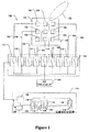
図1を参照すると、アンテナ配列におけるビームを形成するためのデバイス102は、複数の空間的に分散された素子106を有するアンテナ配列104を含む。プロセッサ108は、スイッチ110を通じて所定のパターンで第1及び第2の状態間で素子106を選択的に切り換えるためにアンテナ配列104に結合され、第1の状態では、素子は、着信位置決め信号を受信するように構成され、第2の状態では、素子は、着信位置決め信号を受信しないように構成される。
Referring to FIG. 1, a
位置決め受信機は、アンテナ配列及び基準信号を生成するためのプロセッサと作動的に関連付けられており、そのそれぞれの第1の状態に切り換えられる各素子と実質的に同期して基準信号の位相及び/又は利得を選択的に操作することによって提供される。これは、修正された基準信号を作成し、これは、次に、受信した位置決め信号と混合されて混合信号を作成する。この混合信号は、次に、累積信号がアンテナ配列のビームの方向及び大きさを示すことができるように所定の積分期間にわたって累積される。 The positioning receiver is operatively associated with an antenna array and a processor for generating a reference signal, the reference signal phase and / or substantially synchronized with each element switched to its respective first state. Or provided by selectively manipulating the gain. This creates a modified reference signal, which is then mixed with the received positioning signal to create a mixed signal. This mixed signal is then accumulated over a predetermined integration period so that the accumulated signal can indicate the beam direction and magnitude of the antenna array.
一実施形態では、個別の構成要素/論理ブロックが、混合器、発振器、及び累積器を利用する回路で使用され、次の処理のために位置決め受信機に渡す前に必要な累積信号を生成する。 In one embodiment, separate components / logic blocks are used in circuits utilizing mixers, oscillators, and accumulators to generate the necessary accumulated signals before passing them to the positioning receiver for further processing. .
しかし、好ましい実施形態は、図4に示すように、本発明のビーム形成方法を標準的な位置決め受信機に組み込むことである。これは、本発明によるビーム形成のための必要な回路の殆どが、既に標準的な位置決め受信機アーキテクチャの一部であり、同時ビームの形成を可能にするための軽微な修正を必要とするのみであるからである。当業者が理解するように、相関器において実施されるこの必要な回路は、混合器、発振器、及び累積器を含む。相関器のこれらの構成要素は、個別の構成要素の代わりに利用することができる。これは、コスト及び電力節約の恩典、並びに受信機デバイスの小型化、統合、及び可搬性における付加的な恩典を提供する。 However, the preferred embodiment is to incorporate the beamforming method of the present invention into a standard positioning receiver, as shown in FIG. This is because most of the necessary circuitry for beamforming according to the present invention is already part of the standard positioning receiver architecture and only requires minor modifications to allow simultaneous beamforming. Because. As those skilled in the art will appreciate, this necessary circuit implemented in the correlator includes a mixer, an oscillator, and an accumulator. These components of the correlator can be used instead of individual components. This provides cost and power saving benefits, as well as additional benefits in receiver device miniaturization, integration, and portability.
図1を再度参照すると、位置決めシステムで使用される位置決め受信機114が、好ましい実施形態に従って示されている。位置決め受信機114は、アンテナ配列104及びプロセッサ118に作動的に関連付けられた少なくとも1つの相関器118を有する少なくとも1つの受信チャンネル116を含む既存の構成要素を使用する。各相関器118は、基準信号を生成するための搬送波数値制御発振器(NCO)を組み込んでいる。この基準信号は、その第1の状態に切り換えられる各素子と実質的に同期してプロセッサ108によって修正されたその位相及び/又は利得を有することができ、従って、修正された基準信号を作成する。受信した位置決め信号は、続いて、混合信号を作成するために、この修正された基準信号と混合される。次に、この混合信号は、標準的な相関器処理により符号NCO基準信号と混合され、続いて累積信号を作成するために所定の積分期間にわたって累積される。得られる累積信号は、従って、アンテナ配列104からの相関器118内で形成されたビーム122の方向及び大きさを示すことができる。各々の所定の積分期間の終わりに、相関器ロックループが、位相及び/又は利得操作によって摂動を受けない通常の相関器作動に従って作動する。
Referring again to FIG. 1, a
基準信号の修正
基準信号が搬送波NCOによって合成された後、基準信号は、第1の状態に切り換えられる素子に実質的に同期して基準信号の位相及び/又は利得を選択的に操作することによって修正される。特に、位相及び/又は利得の操作は、位相及び/又は利得オフセットを基準信号に適用することによって達成され、ここで位相及び/又は利得オフセットの値は、第1の状態に切り換えられるそれぞれの素子及びビームが形成される必要な方向に基づいて判断される。
After the modified reference signal of the reference signal is synthesized by the carrier NCO, the reference signal is selectively manipulated in phase and / or gain of the reference signal substantially in synchronism with the element switched to the first state. Will be corrected. In particular, phase and / or gain manipulation is achieved by applying a phase and / or gain offset to the reference signal, where the value of the phase and / or gain offset is each element switched to the first state. And based on the required direction in which the beam is formed.
アンテナ配列104は、相関器回路内のそれぞれの位相及び/又は利得オフセットの挿入を通じて相関器118に作動的に関連付けられる。相関器の作動及び位相及び利得オフセットの挿入は、図4に関して以下に更に詳しく説明する。
The
実施形態では、位相及び/又は利得オフセットの値は、プロセッサによってアクセス可能なデータベース120に記憶されている所定の値を検索することによって判断される。以下の例示的な実施例に示されている表のようなオフセット表が、データベース120に記憶され、プロセッサ108によって選択的にアクセス可能である。所定のオフセット値の記憶されたデータベースが好ましい方法であるが、他の実施形態では、位相及び/又は利得オフセットは、プロセッサ108によってリアルタイムで計算されることが当業者によって理解されるであろう。
In an embodiment, the phase and / or gain offset values are determined by searching predetermined values stored in a
アンテナ素子
図1に示す実施形態では、パッチ素子が3x3配列で示されている。しかし、他の実施形態では、単極、双極、又は他の適切なアンテナ素子が利用されることは当業者によって理解されるであろう。本明細書における開示は、多次元を有するアンテナ配列で配置されるアンテナ素子に等しく適用されることが更に理解されるであろう。実際に、多くの実用的な応用において、アンテナ素子は、3次元形状で空間的に分散される。
Antenna Elements In the embodiment shown in FIG. 1, the patch elements are shown in a 3 × 3 array. However, it will be appreciated by those skilled in the art that in other embodiments, monopolar, bipolar, or other suitable antenna elements are utilized. It will be further understood that the disclosure herein applies equally to antenna elements arranged in an antenna array having multiple dimensions. Indeed, in many practical applications, antenna elements are spatially distributed in a three-dimensional shape.
この明細書及び特許請求の範囲全体を通して、「第1の」状態は、素子がアクティブであることを示し、「第2の」状態は、素子が非アクティブであることを示している。非アクティブ状態の実際の実施では、共振又は相互結合の影響を軽減するために素子を非共振性にすることに重点を置くことにより、使用される素子のタイプに依存して変化する。例えば、1/4λ単極素子は、パッチ素子が第2の状態で接地に切り換えられている間は第2の状態で開に切り換えられる。一部の実施形態では、スイッチはまた、第2の状態における50Ωのような抵抗への接続を提供する。無効負荷のような他の条件に切り換えることも第2の状態で可能であることが当業者によって理解されるであろう。 Throughout this specification and claims, a “first” state indicates that the device is active, and a “second” state indicates that the device is inactive. The actual implementation of the inactive state will vary depending on the type of element used by focusing on making the element non-resonant in order to mitigate the effects of resonance or mutual coupling. For example, a 1 / 4λ monopole element is switched open in the second state while the patch element is switched to ground in the second state. In some embodiments, the switch also provides a connection to a resistor, such as 50Ω, in the second state. It will be appreciated by those skilled in the art that switching to other conditions, such as a reactive load, is also possible in the second state.
ビーム形成スロット
好ましい実施形態では、一度に1つの素子106だけが、所定の積分期間中に第1の状態にあり、一方で全ての他の素子が第2の状態にある。すなわち、形成された各ビームに対して、1つの素子106だけが、積分期間内のいずれの瞬間にも着信信号を受信することができる。各素子106は、所定の積分期間よりも短いいわゆる小積分期間にわたって第1の状態に切り換えられる。一実施形態では、これらの小積分期間は、「ビーム形成スロット」(Bスロット)として公知である。
Beamforming Slot In the preferred embodiment, only one
Bスロットと積分期間の関係は、図2に詳しく示されている。図2の実施例では、Bスロット202は、各々が長さ1μsであり、積分期間はNμs長である。本質的に、積分期間の長さは、いずれかの等しい長さのBスロットに単純に分割される。Bスロットは、従って、単に、第1の状態に切り換えられる関連の素子が着信位置決め信号を受信する期間である。
The relationship between the B slot and the integration period is shown in detail in FIG. In the embodiment of FIG. 2, each
一実施形態では、素子106は、Bスロットに動的に割り当てられる。以下に説明するブライトサイド走査モード作動のようなある一定の用途では、アンテナ配列における素子の部分集合だけがビームを形成するのに必要とされる。これは、信号がこれらの素子から受信されず、従って、累積されないように、積分期間の持続時間全体にわたって第2の状態に切り換えられたままにするように不要な素子を設定することによって達成することができる。代替的に、Bスロットの長さは、延長することができ、それによって素子の部分集合のみがBスロットを割り当てられ、従って、素子のその部分集合から受信した信号だけが累積される。
In one embodiment,
しかし、別の実施形態では、必要なBスロットの最小数は、アンテナ配列104において空間的に分散されている素子106の数に対応する。例えば、アンテナ配列が2つの素子だけを含む実施では、必要なBスロットの最小数は2である。各素子106は、その割り当てられたBスロットの持続時間全体にわたって第1の状態に切り換えられる。
However, in another embodiment, the minimum number of required B slots corresponds to the number of
更に別の実施形態では、10の素子が、アンテナ配列で空間的に分散され、10のBスロットが各素子に対して1つ提供される。標準的なGPS受信機の一般的な積分期間である1000μsの積分期間を使用して、素子は、所定の方式(連続的に又は疑似ランダムに)で各々100μsの期間にわたって第1の状態に切り換えられる。第1の素子が第1の状態に切り換えられた時に、プロセッサはまた、位置決め受信機によって必要な配列内の第1の素子の位置及びビームの方向に対応する基準信号に適用する必要がある位相及び/又は利得オフセットを判断し、かつオフセットを第1の割り当てられたBスロットの持続時間全体にわたって基準信号に適用する。次の100μsBスロットでは、第1の素子及び他の素子の全てがその第2の状態に切り換えられている間、第2の素子が第1の状態に切り換えられる。また、プロセッサは、位置決め受信機によって必要な配列内の第2の素子の位置及びビームの方向に対応する位相及び/又は利得オフセットを判断し、第2のBスロットの持続時間全体にわたって対してその位相及び/又は利得オフセットを適用する。連続的なスイッチング方式を使用するこの実施例では、他の素子が、その積分期間内に次のBスロットに対してその第2の状態などに切り換えられる間、第3の素子は、第3のBスロットで第1の状態に切り換えられる。1000μs積分期間の終了時に、全ての10の100μsBスロットが、必要な位相及び/又は利得オフセットによって累積されることになり、位置決め受信機によって必要なビームを生成する。 In yet another embodiment, 10 elements are spatially distributed in the antenna array and 10 B slots are provided, one for each element. Using an integration period of 1000 μs, which is a typical integration period of a standard GPS receiver, the element switches to a first state over a period of 100 μs each in a predetermined manner (continuously or pseudo-randomly). It is done. When the first element is switched to the first state, the processor also needs to be applied by the positioning receiver to a reference signal corresponding to the position of the first element and the beam direction in the required array. And / or determining a gain offset and applying the offset to the reference signal for the entire duration of the first assigned B slot. In the next 100 μs B slot, the second element is switched to the first state while all of the first element and all other elements are switched to its second state. The processor also determines the phase and / or gain offset corresponding to the position of the second element and the beam direction in the array required by the positioning receiver and for that over the entire duration of the second B slot. Apply phase and / or gain offset. In this embodiment using a continuous switching scheme, the third element is the third element while the other element is switched to its second state, etc. for the next B slot within its integration period. It is switched to the first state at the B slot. At the end of the 1000 μs integration period, all ten 100 μs B slots will be accumulated with the required phase and / or gain offset to produce the required beam by the positioning receiver.
アンテナ配列104における個々の素子106は、第1の状態に切り換えられた時だけ受信機にアクセス可能である。形成されるビームの方向が推測的に既知であるので、素子は、必要な方向にビームを形成するために、基準信号の位相及び/又は利得の適切な操作に実質的に同期して第1の状態に切り換えなくてはならないことになる。また、割り当てられたBスロットの全ての恩典を得るために、割り当てられたBスロットの全てを通して位相及び/又は利得操作を基準信号に適用しなくてはならないことになる。
ビーム形成方法
本明細書に開示するデバイスを使用してビームを形成するための以下の段階は、図3の流れ図に示されている。用いられる段階の説明を以下に提供する。
a)段階301で、アンテナ配列に空間的に分散された素子の1つが選択され、第1Bスロットで第1の状態に切り換えられる。
b)段階302で、段階301で第1の状態に切り換えられた素子が着信信号を受信する。
c)段階304で、着信信号は、アンテナ配列のRFフロントエンドでサンプリングされる。
d)段階308で、内部基準信号が、着信信号と混合するために相関器において生成される。
e)段階310で、所定のオフセットが、段階302と実質的に同期して基準信号に適用され、修正された基準信号を作成する。
f)段階312で、修正された基準信号が、受信した信号と混合され、混合信号を作成する。
g)段階314で、混合信号が、累積信号を作成するために累積器に累積される。
h)段階306で、選択された素子が、第2の状態に切り換えられ、次の素子が、次のBスロットで第1の状態に切り換えられ、処理は、再度段階301から開始される。
i)段階316で、積分期間の終わりにBスロット全てを一緒に累積した後、ビームが、Bスロット信号全ての値に基づいて累積器で形成される。
j)段階318で、搬送波及び符号ロックループが、累積されたBスロット信号を使用して更新される。
Beam Forming Method The following steps for forming a beam using the devices disclosed herein are illustrated in the flow diagram of FIG. A description of the steps used is provided below.
a) In
b) In
c) At
d) At
e) At
f) At
g) At
h) In step 306, the selected element is switched to the second state, the next element is switched to the first state in the next B slot, and the process begins again at
i) In
j) At
相関器の作動
GPS位置受信機は、一般的に、内部で生成された基準信号と着信位置決め信号を相関付けるために、相関器と呼ぶ論理ブロックを使用する。図4を参照すると、相関器118では、着信位置決め信号が、2つの内部で生成された基準信号と混合される。第1の基準信号は、搬送波NCO408によって生成された搬送波基準信号である。搬送波基準信号を着信位置決め信号と混合することで、搬送波基準信号と着信信号間の位相及び周波数の差を表す誤差信号を生成する。第2の基準信号は、この実施形態では符号NCO416によって生成された符号基準信号である。着信位置決め信号が搬送波基準信号と混合された状態で、着信位置決め信号は、符号基準信号と混合され、符号基準信号と着信位置決め信号間の時間遅延を表す誤差信号を生成する。
Correlator Operation GPS position receivers typically use a logic block called a correlator to correlate internally generated reference signals with incoming positioning signals. Referring to FIG. 4, in
簡単にするために、図4は、位置決め受信機の単一の受信チャンネルだけを示している。しかし、当業者は、最新の受信機が、1つよりも多い相関器を各チャンネルが一般的に含む単一の受信チャンネルよりも多い受信チャンネルを一般的に含むことを理解するであろう。 For simplicity, FIG. 4 shows only a single receive channel of the positioning receiver. However, those skilled in the art will appreciate that modern receivers typically include more than one receive channel, each channel typically including more than one correlator.
図4では、着信位置決め信号が、入力402で受信され、混合器404及び406で着信信号を基準搬送波信号と混合することにより搬送波成分を剥ぎ取り、同相(I)及び4相(Q)サンプルデータを生成する。基準搬送波信号は、搬送波NCO408及び離散正弦及び余弦マッピング関数410及び412それぞれで合成される。この剥ぎ取り処理は、図のようにI及びQ信号を生成する。作動において、搬送波NCOは、搬送波ロックループ414によって制御される。搬送波ロックループの目的は、基準信号と着信位置信号間の位相誤差をゼロに又はできるだけゼロの近くに維持することである。位相誤差がゼロである時に、信号は、「位相ロック」であるといわれ、I信号は、Q信号が実質的にゼロである間は最大である。この作動はまた、「位相ロックループ」(PLL)作動と呼ばれる。
In FIG. 4, an incoming positioning signal is received at
次に、I及びQ信号は、この実施形態では符号NCO416で合成される基準符号信号に相関付けられる。簡単にするために、1つの基準符号信号だけがこの実施形態では合成される。しかし、当業者は、殆どの位置決め受信機で、1つよりも多い符号基準信号が合成されることを理解するであろう。例えば、1つの用途では、早期、プロンプト、及び後の信号である3つの符号基準信号は、I及びQ信号によってそれぞれ合成され、別々に相関付けられる。
The I and Q signals are then correlated to a reference code signal synthesized in this embodiment at
相関器118は、内部で合成された符号基準信号を混合器418及び420において着信I及びQ信号と混合する。作動において、符号NCO416は、符号ロックループ426によって制御される。符号ロックループの目的は、内部で生成された符号基準信号と着信符号位置決め信号間の時間誤差をゼロに又はできるだけゼロの近くに維持することである。時間誤差がゼロである時に、信号は「符号ロック」されていると呼ぶ。この作動はまた、「遅延ロックループ」(DLL)作動と呼ばれる。
すなわち、符号ロックループ426の作動は、搬送波ロックループ414に類似している。基準信号符号位相が着信位置決め信号符号位相に完全に整合している時に、最大相関が達成される。
That is, the operation of the
次に、得られる混合信号は、積分期間にわたって累積器422及び424で積分され、ループ作動を追跡するためのプロセッサによって引き続きアクセスされるIp及びQp信号を提供する。
The resulting mixed signal is then integrated by
積分期間は、受信した信号が累積される時間の長さを示し、従来、衛星の疑似ランダム符号ノイズ長又はその倍数に基づいて判断される。GPSでは、この符号期間は1msであり、従って、受信機における積分期間も、1ms又はそれよりも長く設定される場合が多い。 The integration period indicates the length of time in which the received signal is accumulated, and is conventionally determined based on the pseudo-random code noise length of the satellite or a multiple thereof. In GPS, this code period is 1 ms, so the integration period at the receiver is often set to 1 ms or longer.
位相及び/又は利得オフセット
好ましい実施形態では、着信位置決め信号の位相及び/又は利得を操作するための位相及び/又は利得オフセットは、搬送波基準信号が搬送波NCO408によって合成された後でかつ合成された搬送波基準信号が着信位置決め信号の搬送波成分と混合される前にポイント428で挿入され、搬送波ロックループ414を完了する。この好ましい実施形態では、位相オフセットは、基準信号と合計され、利得オフセットは、基準信号によって乗算される。着信位置決め信号の操作は、相関器の積分期間内に合成された搬送波基準信号を修正することによって達成され、従って、搬送波NCO408又は搬送波ロックループ414の通常の作動に干渉しない。次に、修正された基準信号は、通常の方法で着信位置決め信号と混合され、混合信号は、累積信号を作成するために積分期間にわたって累積器で積分される。
Phase and / or Gain Offset In a preferred embodiment, the phase and / or gain offset for manipulating the phase and / or gain of the incoming positioning signal is determined after the carrier reference signal is synthesized by the
当業者によって公知の通り、波形の積分は、単に、所定の期間、この場合は積分期間にわたるその波形のサンプルの合計である。従って、得られる混合信号の積分(着信信号と基準信号を混合して得られる)は、単に、上述の一実施形態では1msの積分期間である期間にわたるその信号のサンプルの合計である。 As known by those skilled in the art, the integration of a waveform is simply the sum of the samples of that waveform over a predetermined period, in this case the integration period. Thus, the resulting integral of the mixed signal (obtained by mixing the incoming signal and the reference signal) is simply the sum of the samples of that signal over a period that in one embodiment is a 1 ms integration period.
一実施形態では、着信位置決め信号は、RFフロントエンドを通じて75MHzの速度でサンプリングされ、次に、サンプルは、同じく75MHzで合成された修正された基準信号と混合される。この結果、積分期間が10のBスロットから構成される1msである仮定のシステムでは、各Bスロットは、持続時間が100μsであり、従って、着信位置決め信号の7,500サンプルを含む。これらの7,500サンプルの各々の1つは、修正された基準信号と連続的に混合され、混合信号を形成する。修正された基準信号は、基準信号に適用される位相及び/又は利得オフセットに基づいており、基準信号は、相関器の搬送波NCOによって生成される。特に、第1の状態にあるアンテナ素子に同期化されている着信位置決め信号の7,500サンプルの各ブロックに対して、基準信号は、位相及び/又は利得オフセットを搬送波NCOの出力に適用することによって修正される。次に、この修正された出力は、着信位置決め信号サンプルによって乗算される(混合される)。次に、これらの混合信号は、通常の相関器作動に従って符号NCO混合器を通過し、次に、累積信号を形成するために累積器で合計される。従って、1msの全積分期間にわたって、75,000サンプルが、各々7,500の修正サンプルの10Bスロットブロックを組み込んで累積器で合計されて記憶される。換言すると、これらの10のBスロットは、7,500修正サンプルを含み、その各々は、累積処理で互いに合計され、従って、積分期間の終わりの75,000累積サンプルは、必要なビームを表している。 In one embodiment, the incoming positioning signal is sampled at a rate of 75 MHz through the RF front end, and then the sample is mixed with a modified reference signal that is also synthesized at 75 MHz. As a result, in the hypothetical system where the integration period is 1 ms consisting of 10 B slots, each B slot is 100 μs in duration and thus contains 7,500 samples of the incoming positioning signal. One of each of these 7,500 samples is continuously mixed with the modified reference signal to form a mixed signal. The modified reference signal is based on the phase and / or gain offset applied to the reference signal, which is generated by the correlator carrier NCO. In particular, for each block of 7,500 samples of the incoming positioning signal that is synchronized to the antenna element in the first state, the reference signal applies a phase and / or gain offset to the output of the carrier NCO. Is fixed by. This modified output is then multiplied (mixed) by the incoming positioning signal samples. These mixed signals are then passed through a sign NCO mixer according to normal correlator operation and then summed in the accumulator to form a cumulative signal. Thus, over the entire integration period of 1 ms, 75,000 samples are summed and stored in an accumulator incorporating 10B slot blocks of 7,500 modified samples each. In other words, these 10 B slots contain 7,500 modified samples, each of which is summed together in the accumulation process, so the 75,000 accumulated samples at the end of the integration period represent the required beam. Yes.
位相及び/又は利得操作が基準信号に適切に適用され、それぞれの素子から受信した信号と混合された状態で、次に、得られる混合信号は、累積器で結合され(合計処理)、相関器において必要なビームを形成する累積信号を作成する。この累積信号は、次に、上述の通常のPLL作動により相関器において処理される。搬送波NCO408によって合成された搬送波基準信号は、積分期間中は変化しないが、各積分期間の最後に搬送波ロックループ414によってのみ更新される。従って、積分期間内の基準信号の修正は、PLL又はDLLによって検出することができない。PLL及びDLLは、起こっている操作に気付かず、通常通りに作動する。
With the phase and / or gain operations appropriately applied to the reference signal and mixed with the signals received from the respective elements, the resulting mixed signals are then combined in an accumulator (summing) and a correlator. A cumulative signal is formed that forms the required beam at. This accumulated signal is then processed in the correlator by the normal PLL operation described above. The carrier reference signal synthesized by the
説明する実施形態を通して、従来の相関器の使用は、相関器チャンネル当たりの固有のビームの方向及び幅を制御するように適応可能であり、それによって複数の同時ビームを形成することができる。形成することができるビームの数は、利用可能な相関器チャンネルの数に等しい。これは、相関器が信号を混合及び積分するための論理を既に収容するためであり、これらは、単に、相関付けること以外の使用に適応されている。 Throughout the described embodiments, the use of conventional correlators can be adapted to control the direction and width of the unique beam per correlator channel, thereby forming multiple simultaneous beams. The number of beams that can be formed is equal to the number of available correlator channels. This is because the correlator already contains the logic to mix and integrate the signals, which are adapted for use other than simply correlating.
上述の実施形態は、相関器回路においてポイント428で利得及び位相の両方にオフセットを適用するが、他の実施形態では、利得オフセットを適用するための付加的な乗算器が、回路の他の部分に提供される。例えば、乗算器は、搬送波NCO混合器と符号NCO混合器間の同相及び4相経路に追加することができ、利得操作を提供する。同様に、位相オフセットはまた、相関器回路の他の部分で適用することができる。例えば、位相オフセットは、符号NCOの出力に追加することができる。
While the above embodiments apply an offset to both gain and phase at
好ましい実施形態では、あらゆる所定の方向にビームを形成するための位相及び/又は利得オフセットが事前に判断されており、データベース120に記憶され、プロセッサ108によってアクセス可能である。オフセットデータのフォーマットは、オフセット表のような多くの形式を取ることができる。プロセッサ108は、要求されたビームの方向を判断し、必要な方向にビームを形成するために積分期間にわたって各Bスロットにおける各素子に対する正確な位相及び/又は利得オフセットを得るためにデータベース120にアクセスし、ポイント428で必要なオフセットを挿入し、それによってビーム(図1の122)が、適切な着信位置決め信号の方向に形成される。説明するように、位相及び/又は利得オフセットを取得及び挿入する段階は、位相及び/又は利得が積分期間にわたって正確に操作されるように、第1の状態へのそれぞれの素子の切り換えに実質的に同期すべきである。
In the preferred embodiment, the phase and / or gain offset for forming the beam in any given direction is pre-determined and stored in the
一実施形態では、アンテナ配列は、128の素子を有する。従って、各方向は、オフセット表で128の位相及び128の利得エントリを有する。例えば、ビームを北に向ける必要がある場合、プロセッサは、北への表エントリをルックアップし、積分期間にわたるその方向への128位相及び128利得エントリの各々を段階的に通過し、ビームを北に向ける。この実施形態では、各方向が128位相及び128利得エントリを有する2048方向にビームを向けることができる。勿論、他の実施形態では、より多くの方向が実行される。この理由のために、処理のオーバヘッドを軽くするために、位相及び/又は利得オフセット値を表形式で提供することが好ましい。 In one embodiment, the antenna array has 128 elements. Thus, each direction has 128 phases and 128 gain entries in the offset table. For example, if the beam needs to be directed north, the processor looks up the table entry to north, stepping through each of 128 phase and 128 gain entries in that direction over the integration period, Turn to. In this embodiment, the beam can be directed in 2048 directions, each direction having 128 phases and 128 gain entries. Of course, in other embodiments, more directions are performed. For this reason, it is preferable to provide the phase and / or gain offset values in tabular form to reduce processing overhead.
上述の段落に示す実施形態は、これが必要な処理機能を最小限にするので好ましい。しかし、当業者は、特にマイクロプロセッサ技術における最近の進歩を考えると、オフセットが要求されるのでかつその時に、位相及び/又は利得オフセットを計算するようにプロセッサ108を構成することができることを理解するであろう。
The embodiment shown in the above paragraph is preferred because it minimizes the required processing functions. However, those skilled in the art will appreciate that the
本発明の物理的な実施では、各素子は、それぞれのスイッチに送信回線124によって接続され、それぞれのスイッチは、次に、少なくとも1つの相関器にダウンコンバートされかつ送信されることになる単一のRFフロントエンド126にフィードする。好ましい実施形態では、素子とスイッチを相互結合する送信回線は、等しい長さであり、受信した信号がアンテナ配列フィードシステムを通じて位相干渉性であるようにすることに注意すべきである。しかし、他の実施形態では、送信回線の長さの違いは、位相及び/又は利得オフセットを適用する時に考慮に入れられて補正される。
In the physical implementation of the present invention, each element is connected to a respective switch by a
アンテナ配列104と受信チャンネル116間の相互結合、並びにRFフロントエンド126、相関器118に含まれる電子機器、及び実際のスイッチ110自体は、必ず遅延を引き起こすことになる。一実施形態では、この遅延は、約950nsであると測定されるが、勿論、当業者は、遅延の長さが、選択されたハードウエアに依存して変わることを理解するであろう。従って、相関器における位相及び/又は利得操作の作動は、この遅延を考慮に入れなくてはならないので、第1の状態への素子の切り換えと同時に実行することはできない。すなわち、相関器における位相及び/又は利得の操作は、この実施形態では950nsまで遅らせなくてはならない。
The mutual coupling between the
他の実施形態では、各アンテナ配列は、100μsの領域の積分期間に60を超える素子を収容する。このような実施形態では、Bスロットの期間は、僅かに1μs又は2μsの領域である。従って、実質的に1μsである950nsの遅延は重大であり、考慮に入れなくてはならない。 In other embodiments, each antenna array accommodates more than 60 elements in the 100 μs region integration period. In such an embodiment, the duration of the B slot is only 1 μs or 2 μs. Therefore, the 950 ns delay, which is substantially 1 μs, is significant and must be taken into account.
アンテナ配列が収容する素子の数は、狭いビームを形成するための1つの基準である。他の等しく重要な基準は、オフセット表の分解能及び素子の物理的間隔を含む。各方向に対して、各素子は、位相及び/又は利得に対する関連付けられたオフセットを持たなくてはならない。例えば、60素子を有する実施形態では、ビームが形成される各方向に対する表エントリは、記録された60利得オフセット及び60位相オフセットを持たなくてはならない。 The number of elements accommodated by the antenna array is one criterion for forming a narrow beam. Other equally important criteria include offset table resolution and element physical spacing. For each direction, each element must have an associated offset to phase and / or gain. For example, in an embodiment with 60 elements, the table entry for each direction in which the beam is formed must have a recorded 60 gain offset and 60 phase offset.
素子の物理的分離も、素子間の位相差を作成するのに重要である。実質的に、素子の物理的分離により、本質的に異なる位相を有する位置決め信号を受信することができる。素子間の2分の1波長分離は、最小格子ローブを有する最大の位相整合を提供する。例えば、上述のように修正された基準信号と混合することによるこれらの位相の操作により、ビームを必要な方向に形成することができる。 The physical separation of the elements is also important for creating the phase difference between the elements. In effect, positioning signals having essentially different phases can be received due to the physical separation of the elements. Half-wave separation between elements provides maximum phase matching with minimum grating lobes. For example, by manipulating these phases by mixing with a reference signal modified as described above, the beam can be formed in the required direction.
特に好ましい実施形態では、素子106は、デバイスが2つよりも多い次元でビームを形成することができるように、2つよりも多い次元の構成で空間的に分散される。大体において、ビームを形成することができる方向は、使用される素子に依存する。例えば、パッチ素子から構成される平面配列は、半球状にビームを形成することができ、単極から構成される平面配列は、平面でビームを形成することができることになる。
In a particularly preferred embodiment, the
ブライトサイド走査モード対全走査モード
以上の説明から、パッチ素子から構成される少なくとも2つの平面配列は、半球状ビームを接合して球状にビームを形成するように配置することができることになる。従って、この構成では、あらゆる方向にビームを形成することができる。
From the above description of the bright side scanning mode versus the full scanning mode, at least two planar arrays composed of patch elements can be arranged so as to form a spherical beam by joining hemispherical beams. Therefore, with this configuration, a beam can be formed in any direction.
全走査モードでは、全ての素子が、積分期間内に少なくとも一度第1及び第2の状態間で切り換えられる。すなわち、配列の素子の全てが、各積分期間内で少なくとも一度着信信号を受信する。全走査モードは、どのくらいの数の相関器チャンネルが利用可能であるかに依存して、多くの異なる方向に同時にビームを形成することができる全体的な柔軟性を提供する。 In full scan mode, all elements are switched between the first and second states at least once during the integration period. That is, all of the elements in the array receive an incoming signal at least once within each integration period. The full scan mode provides the overall flexibility to be able to form beams in many different directions simultaneously, depending on how many correlator channels are available.
しかし、信号が「ブライトサイド」と呼ぶ3次元アンテナ配列の1つの側だけに照射した時に、「ダークサイド」と呼ぶアンテナ配列の他方の側から受信した情報は、潜在的に小さな値になる。この状況は、送信機が地平線に一般的に分散されている地上位置決めシステムで頻繁に発生する。この場合、ダークサイド素子は、ブランクにされており(すなわち、これらの素子における利得はゼロに設定される)、ブライトサイド素子だけが使用される。これは、配列の相関負荷サイクルを50%だけ効率的に低減し、アンテナ配列の相関利得の半分が浪費されることを意味する。比較的小さなエリアに跨がる位置決めシステムでは、送信された信号の信号電力が比較的高いので、アンテナからの相関利得のこの損失は許容できる。従って、最適な柔軟性のために最大相関利得を交換取引することが許容可能である小さなエリアのシステムでは、全走査モードが好ましい。 However, when the signal illuminates only one side of the three-dimensional antenna array called “bright side”, the information received from the other side of the antenna array called “dark side” is potentially a small value. This situation frequently occurs in ground positioning systems where transmitters are generally distributed over the horizon. In this case, the dark side elements are blanked (ie, the gain in these elements is set to zero) and only the bright side elements are used. This effectively reduces the correlation duty cycle of the array by 50%, and half of the correlation gain of the antenna array is wasted. In a positioning system that spans a relatively small area, this loss of correlation gain from the antenna is acceptable because the signal power of the transmitted signal is relatively high. Therefore, full scan mode is preferred in small area systems where it is acceptable to trade the maximum correlation gain for optimal flexibility.
しかし、信号がより遠くの距離にわたって送信される大きな地理的エリアでは、相関利得は、益々重要になる。このような場合、アンテナの相関利得を増すための1つの方法は、ブライトサイド走査モードで作動することである。このモードでは、ブライトサイドにおける素子は、動的に一緒にグループ分けされ、そのそれぞれのBスロット持続時間が増え、それによってブライトサイド素子だけが、積分期間内に累積される。これは、相関負荷サイクルにおける増加、及び従って相関利得における全体的な増加をもたらす。 However, in large geographic areas where signals are transmitted over longer distances, correlation gain becomes increasingly important. In such cases, one way to increase the correlation gain of the antenna is to operate in a bright side scan mode. In this mode, the elements on the bright side are dynamically grouped together, increasing their respective B slot durations, so that only the bright side elements are accumulated within the integration period. This results in an increase in the correlation duty cycle and thus an overall increase in correlation gain.
例示的な実施形態
例示的な目的のために、ここで、本発明を最も単純なアンテナ配列、すなわち、図5a及び5bに示すように2つの素子だけを有する配列を使用して以下に説明する。しかし、当業者は、本明細書の教示を付加的な発明的機能なしに多次元形状で空間的に分散された多くの素子を有するアンテナ配列に適応させることができるであろう。
Exemplary Embodiments For exemplary purposes, the present invention will now be described below using the simplest antenna array, ie, an array having only two elements as shown in FIGS. 5a and 5b. . However, those skilled in the art will be able to adapt the teachings herein to antenna arrays having many elements spatially distributed in a multidimensional shape without additional inventive features.
この例示的な実施形態では、素子502及び504は、1/4波長単極である。2つの素子は、互いに空間的に離れて1/2波長で配置され、信号は、各素子で受信される。2つの素子が互いに合計された時に、素子の2次元上面図から見て8の字のビームパターンが図5aに示すように形成されるように、素子のそれぞれの全方向利得パターンが結合される。この構成では、素子502及び504のブロードサイド方向からの着信位置決め信号は、同相であり、従って、増幅され、一方、素子のエンド−ファイヤ方向からの信号は、位相不一致であり、従って、相殺される。
In this exemplary embodiment,
位相操作
本発明では、最大利得が図5bに示すようにエンド−ファイヤ方向に向くように、90°だけ8の字を回転させることができる。これは、位置受信機の積分期間内に素子502及び素子504の位相及び/又は利得操作することによって達成される。素子502及び素子504の各々は、スイッチに接続され、それによってあらゆる素子を第1及び第2の状態間で切り換えることができ、信号の合計が行われる積分期間は、2つのBスロットに分けられる。
Phase Manipulation In the present invention, the figure 8 can be rotated by 90 ° so that the maximum gain is in the end-fire direction as shown in FIG. 5b. This is accomplished by manipulating the phase and / or gain of
素子502及び504間の位相分離が既知であるので、エンド−ファイヤ方向からの着信波が、破壊的ではなく構成的に合計されるように、素子の1つの位相を操作することができる。この場合、素子は1/2波長離れているので、素子504で必要な位相操作は180°である。各方向に対して必要な位相操作は、オフセット表を構成するために同様に計算される。単純にするために、利得オフセットは1に設定され、ビームを向けることができる方向は、ブロードサイド方向又はエンド−ファイヤ方向のいずれかに制限される。これらの制限を組み込む実施例のオフセット表を以下に示している。
Since the phase separation between
(表)

エンド−ファイヤ方向にビームを形成するために、素子502及び504は、位置受信機の積分期間内で所定のBスロットシーケンスで第1の状態に切り換えられる。第1Bスロットでは、素子502は、第1の状態に切り換えられ、位相オフセットは、累積器で累積される間は0°に維持され、この素子が既に0°であるので操作は必要ない。第2のBスロットでは、着信信号の位相は、素子504で構成的に合計されることが望ましい。素子504は、素子502に対して180°の受信位相を有するので、180°の位相オフセットを累積器で累積される間に素子504に適用しなくてはならず、それによって素子504からの受信した信号は、素子502に干渉する位相になる。2つのBスロットは、従って、累積処理で互いに合計され、積分期間の終わりの累積された値は、エンド−ファイヤビームを表している。
To form a beam in the end-fire direction,
本発明では8の字のビームがオフセット表の複雑さに依存していずれの方向にも形成することができることが、当業者によって理解されるであろう。 It will be appreciated by those skilled in the art that the figure 8 beam can be formed in either direction depending on the complexity of the offset table.
この単純な実施例における両方の素子に対しては、1の利得オフセット(1の利得)が着信位置決め信号と乗算され、従って、形成されたビームを修正しない。 For both elements in this simple embodiment, a gain offset of 1 (gain of 1) is multiplied with the incoming positioning signal and thus does not modify the formed beam.
上述のように、位相操作は、第1の状態への素子の切り換えに実質的に同期して適用すべきであり、そうでなければ、ビームの利得パターンは、正確に形成されない。 As mentioned above, the phase manipulation should be applied substantially synchronously with the switching of the element to the first state, otherwise the beam gain pattern will not be accurately formed.
本発明の実施形態によると、例えば、PRN1からの位置決め信号が、送信を開始する。位置決め受信機でのPRN1の取得後に、位置決め受信機相関器内の搬送波NCOは、位置決め信号に実質的に類似した基準信号を合成する。
According to the embodiment of the present invention, for example, a positioning signal from the
位置決め受信機は、PRN1がエンド−ファイヤ方向であると判断し、従って、その方向のビームを形成する決定が為される。プロセッサは、オフセット表をルックアップし、素子502に対応する積分期間中の第1Bスロットに対して必要なオフセットがないと判断する。同様に、プロセッサは、180°又は1/2λのオフセットが、素子504に対応する第2のBスロット中に必要であると判断する。修正された基準信号を作成するために搬送波NCOに各オフセットを適用した後、着信位置決め信号及び修正された基準信号は、相関器の通常の作動により、混合器で混合され累積器で累積される。すなわち、図1、3、及び5に関して、素子502及び504で受信した着信位置決め信号は、スイッチを通じてRFフロントエンド126にフィードされ、続いてアナログ−デジタル変換器でダウンコンバートされてサンプリングされる。次に、受信した信号は、少なくとも1つの相関器118に送られる。
The positioning receiver determines that PRN1 is in the end-fire direction and therefore a decision is made to form a beam in that direction. The processor looks up the offset table and determines that there is no required offset for the first B slot during the integration period corresponding to
受信した位置決め信号は、受信した位置決め信号を搬送波NCO408及び離散正弦及び余弦マッピング関数410及び412によって合成された搬送波基準信号と混合することにより、その同相及び4相成分に分けられる。しかし、修正された基準信号が、受信した位置決め信号と混合される前に、プロセッサは、PRN1がエンド−ファイヤ方向であると判断する。素子502が第1の状態に切り換えられている第1Bスロットに対して、プロセッサは、搬送波NCOに対するオフセットが必要であるか否かを判断するために表を検査する。この場合、オフセットは必要なく、基準信号への修正も必要ない。従って、累積が通常の相関器作動に従って進行することが許可される。すなわち、修正されていない基準信号が、混合器404及び406で受信した位置決め信号と混合され、混合信号を作成し、次に、符号基準信号と混合され、続いて累積器422及び424で累積される。
The received positioning signal is divided into its in-phase and four-phase components by mixing the received positioning signal with the carrier reference signal synthesized by
第2のBスロットに対して、プロセッサは、搬送波NCOへのオフセットが必要か否かを判断するために表を検査する。この場合、180°の位相オフセットが必要である。オフセットは、第2のBスロットが始まり、素子504が第1の状態に切り換えられる時に、現在の搬送波基準信号位相値に適用されて修正された基準信号を作成する。位相オフセットは、Bスロットの持続時間全体を通して搬送波NCO値に継続して適用される。修正された基準信号は、受信した位置決め信号と混合され、混合信号を作成し、次に、符号基準信号と混合され、続いて累積器422及び424で第1Bスロットの値と共に累積され、累積信号を作成する。2つのBスロットは、従って、累積処理で互いに合計され、積分期間の終わりの累積された値は、従って、エンド−ファイヤビームを表している。
For the second B slot, the processor checks the table to determine if an offset to the carrier NCO is required. In this case, a 180 ° phase offset is required. The offset is applied to the current carrier reference signal phase value to create a modified reference signal when the second B slot begins and
搬送波NCO408によって合成された搬送波基準信号は、積分期間中は変化しないが、積分期間の終わりに搬送波ロックループ414によって更新されるだけであることに注意されたい。
Note that the carrier reference signal synthesized by the
本明細書に説明する実施形態では、累積信号は、積分期間の持続時間全体にわたって累積器で作成される。しかし、他の実施形態では、各Bスロットは、その独自の個々の累積器で累積され、累積器の最小数は、必要なBスロットの最小数に対応する。これらの実施形態では、累積信号は、個々の累積器における信号を結合することから得られる。 In the embodiments described herein, the accumulated signal is generated in an accumulator over the entire duration of the integration period. However, in other embodiments, each B slot is accumulated with its own individual accumulator, and the minimum number of accumulators corresponds to the minimum number of B slots required. In these embodiments, the accumulated signal is obtained from combining the signals at the individual accumulators.
説明した実施形態では、1つの素子だけが、積分期間内のいずれの瞬間にも第1の状態にあることができる。従って、素子504が第1の状態に切り換えられた時に、素子502は、同時に第2の状態に切り換えられる。
In the described embodiment, only one element can be in the first state at any instant in the integration period. Thus, when
符号ロックループ426を行き来した後、混合された信号は、累積器422及び424で積分され、累積信号を作成する。信号への操作が連続して行われるので、混合信号の積分は、実際には、積分期間にわたる無限数の修正された信号の合計である。従って、累積信号は、必要な方向に形成された新しいビームを表している。
After traversing the
上述のように、アンテナ配列104及びスイッチング回路(スイッチ110)は、受信機の位置を判断するために必要なPVT解決法を実行する位置決め受信機114に結合される。着信位置決め信号の方向がいずれの所定の時間に対しても既知であるので、各相関器チャンネルで形成されるビームをそれらの既知の方向に対して向けて着信信号の利得を最大にし、一方、他の方向からの信号を減衰し、従って、多経路の影響を軽減することができる。
As described above, the
本発明を特定的な実施例に関して説明してきたが、本発明は、多くの他の形式で具現化することができることは当業者によって認められるであろう Although the present invention has been described in terms of particular embodiments, it will be appreciated by those skilled in the art that the present invention may be embodied in many other forms.
以下の特許請求の範囲及び本明細書の説明では、用語「comprising」、「comprised of」、又は「which comprises」のいずれも、その他を除外せずに少なくともそれに続く要素/特徴を含むことを意味する未決用語である。従って、特許請求の範囲で使用される「comprising」という用語は、その後に挙げる手段又は要素又は段階に制限するように解釈すべきではない。例えば、A及びBを含むデバイスの表現の範囲は、要素A及びBだけから構成されるデバイスに制限すべきではない。本明細書で使用される用語「including」、「which includes」、又は「that includes」のいずれも、同じくその他を除外せずにその語に続く要素/特徴を少なくとも含むことを意味する未決用語である。従って、「including」は、「comprising」と同義であり、かつ同じことを意味する。 In the claims below and in the description herein, any of the terms “comprising”, “comprised of”, or “who complies” means that at least the following elements / features are included without excluding others. It is a pending term. Accordingly, the term “comprising” as used in the claims should not be construed as limited to the means or elements or steps listed thereafter. For example, the scope of the representation of a device that includes A and B should not be limited to devices that consist only of elements A and B. Any of the terms “including”, “why includes”, or “that includes” as used herein is a pending term that is meant to include at least the elements / features that follow the word without excluding others. is there. Accordingly, “including” is synonymous with “comprising” and means the same thing.
301 アンテナ配列に空間的に分散された素子の1つが選択され、第1Bスロットで第1の状態に切り換えられる段階
302 段階301で第1の状態に切り換えられた素子が着信信号を受信する段階
304 着信信号が、アンテナ配列のRFフロントエンドでサンプリングされる段階
308 内部基準信号が、着信信号と混合するために相関器において生成される段階
301 One of the elements spatially distributed in the antenna array is selected and switched to the first state in the
Claims (21)
複数の空間的に分散された素子を有するアンテナ配列と、
第1及び第2の状態の間で前記素子を選択的に切り換えるためのプロセッサであって、該第1の状態では、該素子が着信信号を受信するように構成され、該第2の状態では着信信号を受信しないように構成される前記プロセッサと、
前記アンテナ配列及び前記プロセッサと作動的に関連付けられた受信器であって、前記受信器は、基準信号を生成し、前記第1の状態に切り替えられている前記素子に実質的に同期して前記基準信号を修正し、混合信号を生成するために前記着信信号を前記修正された基準信号と混合し、かつ累積信号を生成するために積分期間にわたって該混合信号を合計し、該累積信号が該アンテナ配列の前記ビームの方向及び大きさを示すことができるように構成された受信機と、
を含むことを特徴とするデバイス。 A device for forming a beam of an antenna array,
An antenna array having a plurality of spatially dispersed elements;
A processor for selectively switching the element between first and second states, wherein the element is configured to receive an incoming signal in the first state, and in the second state, The processor configured to not receive an incoming signal;
A receiver operatively associated with the antenna array and the processor, wherein the receiver generates a reference signal and is substantially synchronized with the element being switched to the first state. Modifying the reference signal, mixing the incoming signal with the modified reference signal to generate a mixed signal, and summing the mixed signal over an integration period to generate an accumulated signal, the accumulated signal being A receiver configured to be able to indicate the direction and size of the beam of the antenna array;
A device comprising:
ことを特徴とする請求項1に記載のデバイス。 The receiver includes at least one receive channel having a correlator configured to generate the reference signal;
The device according to claim 1.
前記位相及び/又は利得オフセットの値が、前記第1の状態に切り換えられる前記素子の1つに基づいて判断される、
ことを特徴とする請求項3に記載のデバイス。 The manipulation of the phase and / or gain comprises applying a phase and / or gain offset to the reference signal;
A value of the phase and / or gain offset is determined based on one of the elements switched to the first state;
The device according to claim 3.
各受信チャンネルが、少なくとも1つのビームを形成するように適応可能である、
ことを特徴とする請求項1又は2に記載のデバイス。 The receiver includes a plurality of receiving channels;
Each receive channel is adaptable to form at least one beam;
The device according to claim 1 or 2, characterized in that
a)空間的に分散されたアンテナ配列の素子を、該素子が着信信号を受信しないように構成される第2の状態から該素子が着信信号を受信するように構成される第1の状態に選択的に切り換える段階と、
b)前記第1の状態に切り換えられた前記素子を通じて前記着信信号を受信する段階と、
c)基準信号を生成する段階と、
d)前記第1の状態に切り換えられている前記素子に実質的に同期して前記基準信号を修正する段階と、
e)前記着信信号を前記修正された基準信号と混合して混合信号を作成する段階と、
f)積分期間にわたって前記混合信号を累積し、前記アンテナ配列のビームの方向及び大きさを示す累積信号を作成する段階と、
を含むことを特徴とする方法。 A method of forming an antenna array beam comprising:
a) The elements of the spatially distributed antenna arrangement are changed from a second state in which the elements are configured not to receive incoming signals to a first state in which the elements are configured to receive incoming signals. Selectively switching, and
b) receiving the incoming signal through the element switched to the first state;
c) generating a reference signal;
d) modifying the reference signal substantially synchronously with the element being switched to the first state;
e) mixing the incoming signal with the modified reference signal to create a mixed signal;
f) accumulating the mixed signal over an integration period to create an accumulated signal indicative of the beam direction and magnitude of the antenna array;
A method comprising the steps of:
ことを特徴とする請求項12に記載の方法。 The reference signal is generated by a correlator;
The method according to claim 12.
前記位相及び/又は利得オフセットの値が、前記第1の状態に切り換えられる前記素子の1つに基づいて判断される、
ことを特徴とする請求項14に記載の方法。 It said selective operation of said phase and / or gain of the reference signal includes the application to the reference signal position phase and / or gain offset,
A value of the phase and / or gain offset is determined based on one of the elements switched to the first state;
15. The method of claim 14, wherein:
前記受信機が、複数の受信チャンネルを含み、
前記方法は、各受信チャンネルが、少なくとも1つのビームを形成するように適応させるステップを更に含む、
ことを特徴とする請求項12又は13に記載の方法。 The method is performed by a receiver in operative association with the antenna array;
The receiver includes a plurality of receiving channels;
The method further includes adapting each receive channel to form at least one beam;
14. A method according to claim 12 or 13, characterized in that
Applications Claiming Priority (3)
| Application Number | Priority Date | Filing Date | Title |
|---|---|---|---|
| AU2009903063 | 2009-07-01 | ||
| AU2009903063A AU2009903063A0 (en) | 2009-07-01 | Method and Apparatus for Forming a Gain Pattern | |
| PCT/AU2010/000839 WO2011000049A1 (en) | 2009-07-01 | 2010-07-01 | Method and apparatus for forming a beam |
Related Child Applications (1)
| Application Number | Title | Priority Date | Filing Date |
|---|---|---|---|
| JP2015032134A Division JP5980358B2 (en) | 2009-07-01 | 2015-02-20 | Method and apparatus for forming a beam |
Publications (3)
| Publication Number | Publication Date |
|---|---|
| JP2012531597A JP2012531597A (en) | 2012-12-10 |
| JP2012531597A5 JP2012531597A5 (en) | 2013-08-15 |
| JP5702775B2 true JP5702775B2 (en) | 2015-04-15 |
Family
ID=43410374
Family Applications (2)
| Application Number | Title | Priority Date | Filing Date |
|---|---|---|---|
| JP2012517981A Active JP5702775B2 (en) | 2009-07-01 | 2010-07-01 | Method and apparatus for forming a beam |
| JP2015032134A Active JP5980358B2 (en) | 2009-07-01 | 2015-02-20 | Method and apparatus for forming a beam |
Family Applications After (1)
| Application Number | Title | Priority Date | Filing Date |
|---|---|---|---|
| JP2015032134A Active JP5980358B2 (en) | 2009-07-01 | 2015-02-20 | Method and apparatus for forming a beam |
Country Status (9)
| Country | Link |
|---|---|
| US (3) | US8934844B2 (en) |
| EP (1) | EP2449627B1 (en) |
| JP (2) | JP5702775B2 (en) |
| KR (1) | KR101709804B1 (en) |
| CN (1) | CN102474006B (en) |
| ES (1) | ES2654641T3 (en) |
| IL (2) | IL216478A (en) |
| SG (1) | SG176616A1 (en) |
| WO (1) | WO2011000049A1 (en) |
Cited By (1)
| Publication number | Priority date | Publication date | Assignee | Title |
|---|---|---|---|---|
| JP2015127712A (en) * | 2009-07-01 | 2015-07-09 | ロケイタ コーポレイション プロプライエタリー リミテッド | Method and apparatus for forming beam |
Families Citing this family (12)
| Publication number | Priority date | Publication date | Assignee | Title |
|---|---|---|---|---|
| US9640865B2 (en) | 2010-10-21 | 2017-05-02 | Locata Corporation Pty Ltd | Method and apparatus for forming a remote beam |
| JP2014505726A (en) | 2011-02-15 | 2014-03-06 | イーライ リリー アンド カンパニー | Method for inhibiting pain in dogs using a transdermal solution of fentanyl |
| FR2988483B1 (en) * | 2012-03-22 | 2014-03-07 | Thales Sa | DEVICE FOR RECEIVING MULTI-ANTENNA RADIO NAVIGATION SIGNALS |
| US11125888B2 (en) * | 2016-06-06 | 2021-09-21 | Brian G. Agee | Multi-subband methods for reduced complexity, wideband blind resilient detection and geo-observable estimation of global navigation satellite signals |
| US10775510B2 (en) | 2016-06-06 | 2020-09-15 | Brian G. Agee | Blind despreading of civil GNSS signals for resilient PNT applications |
| JP7179768B2 (en) * | 2017-05-12 | 2022-11-29 | ロケイタ コーポレイション プロプライエタリー リミテッド | Method and apparatus for characterizing user platform environment |
| KR102105449B1 (en) * | 2017-09-11 | 2020-05-29 | 한국과학기술원 | Beam-forming circuit for 5g mobile communication and radar |
| CN111869004B (en) * | 2018-03-22 | 2022-04-19 | 康普技术有限责任公司 | Base station antenna supporting high Effective Isotropic Radiated Power (EIRP) with high boresight coverage using linear superposition of amplitude and phase weighting |
| CN108511909B (en) * | 2018-05-08 | 2020-08-07 | 鹰视云(深圳)科技有限公司 | Array arrangement method of spherical phased array antenna |
| WO2020027391A1 (en) * | 2018-08-03 | 2020-02-06 | 경상대학교 산학협력단 | Array antenna apparatus having wide elevation |
| KR102019432B1 (en) * | 2018-08-03 | 2019-09-06 | 경상대학교 산학협력단 | Array antenna apparatus for wide elevation |
| KR102019434B1 (en) * | 2018-09-06 | 2019-09-06 | 경상대학교 산학협력단 | Array antenna arranged in horizontal direction along y-axis for wide elevation |
Family Cites Families (24)
| Publication number | Priority date | Publication date | Assignee | Title |
|---|---|---|---|---|
| FR1344349A (en) * | 1962-10-02 | 1963-11-29 | Csf | Electronic scanning curtain antenna |
| US5103232A (en) | 1991-04-18 | 1992-04-07 | Raytheon Company | Phase quantization error decorrelator for phased array antenna |
| US5268695A (en) | 1992-10-06 | 1993-12-07 | Trimble Navigation Limited | Differential phase measurement through antenna multiplexing |
| US6289004B1 (en) * | 1998-03-12 | 2001-09-11 | Interdigital Technology Corporation | Adaptive cancellation of fixed interferers |
| US6411612B1 (en) * | 1998-05-19 | 2002-06-25 | Harris Communication | Selective modification of antenna directivity pattern to adaptively cancel co-channel interference in TDMA cellular communication system |
| US6304216B1 (en) * | 1999-03-30 | 2001-10-16 | Conexant Systems, Inc. | Signal detector employing correlation analysis of non-uniform and disjoint sample segments |
| US6005515A (en) * | 1999-04-09 | 1999-12-21 | Trw Inc. | Multiple scanning beam direct radiating array and method for its use |
| JP3597101B2 (en) | 2000-02-21 | 2004-12-02 | 埼玉日本電気株式会社 | Receiver circuit and adaptive array antenna system |
| US6928275B1 (en) * | 2000-05-08 | 2005-08-09 | Qualcomm Incorporated | Method and apparatus for compensating local oscillator frequency error |
| JP4028178B2 (en) | 2001-02-09 | 2007-12-26 | 株式会社東芝 | Mobile antenna device |
| DE10125474A1 (en) * | 2001-05-25 | 2002-12-12 | Walter Doell | Device and method for receiving signals emitted by satellites |
| JP2003023383A (en) | 2001-07-06 | 2003-01-24 | Mitsubishi Heavy Ind Ltd | Variable beam antenna system |
| EP1442498B1 (en) | 2001-11-09 | 2006-08-09 | EMS Technologies, Inc. | Beamformer for multi-beam receive antenna |
| US6828935B1 (en) | 2002-07-19 | 2004-12-07 | The United States Of America As Represented By The Administrator Of The National Aeronautics And Space Administration | Digitally synthesized phased antenna for multibeam global positioning |
| US6870503B2 (en) * | 2002-11-19 | 2005-03-22 | Farrokh Mohamadi | Beam-forming antenna system |
| JP3858873B2 (en) | 2002-12-02 | 2006-12-20 | 株式会社村田製作所 | Antenna device, radio device and radar |
| JP2004317524A (en) * | 2004-07-30 | 2004-11-11 | Fujitsu Ltd | Radar system |
| US7460615B2 (en) | 2005-04-12 | 2008-12-02 | Novatel, Inc. | Spatial and time multiplexing of multi-band signals |
| JP2006345426A (en) * | 2005-06-10 | 2006-12-21 | Matsushita Electric Ind Co Ltd | Receiving device, receiving method, and program |
| JP4646220B2 (en) * | 2005-07-14 | 2011-03-09 | 古河電気工業株式会社 | Modulator, communication device and short-range radar |
| PL1991881T3 (en) * | 2006-03-09 | 2017-12-29 | European Space Agency | A receiver and transmitter for use in a satellite navigation system |
| JP4138825B2 (en) * | 2006-07-26 | 2008-08-27 | 株式会社東芝 | Weight calculation method, weight calculation device, adaptive array antenna, and radar device |
| US7786933B2 (en) | 2007-05-21 | 2010-08-31 | Spatial Digital Systems, Inc. | Digital beam-forming apparatus and technique for a multi-beam global positioning system (GPS) receiver |
| US8934844B2 (en) * | 2009-07-01 | 2015-01-13 | Locata Corporation Pty Ltd | Method and apparatus for forming a beam |
-
2010
- 2010-07-01 US US13/377,808 patent/US8934844B2/en active Active
- 2010-07-01 JP JP2012517981A patent/JP5702775B2/en active Active
- 2010-07-01 WO PCT/AU2010/000839 patent/WO2011000049A1/en active Application Filing
- 2010-07-01 EP EP10793437.4A patent/EP2449627B1/en active Active
- 2010-07-01 SG SG2011088309A patent/SG176616A1/en unknown
- 2010-07-01 CN CN201080028927.6A patent/CN102474006B/en active Active
- 2010-07-01 ES ES10793437.4T patent/ES2654641T3/en active Active
- 2010-07-01 KR KR1020117029544A patent/KR101709804B1/en active IP Right Grant
-
2011
- 2011-11-20 IL IL216478A patent/IL216478A/en active IP Right Grant
-
2014
- 2014-12-01 US US14/557,412 patent/US9444539B2/en active Active
-
2015
- 2015-02-20 JP JP2015032134A patent/JP5980358B2/en active Active
-
2016
- 2016-04-07 IL IL244992A patent/IL244992A/en active IP Right Grant
- 2016-08-02 US US15/226,903 patent/US9739887B2/en active Active
Cited By (1)
| Publication number | Priority date | Publication date | Assignee | Title |
|---|---|---|---|---|
| JP2015127712A (en) * | 2009-07-01 | 2015-07-09 | ロケイタ コーポレイション プロプライエタリー リミテッド | Method and apparatus for forming beam |
Also Published As
| Publication number | Publication date |
|---|---|
| US20170068000A1 (en) | 2017-03-09 |
| IL216478A (en) | 2016-04-21 |
| IL244992A0 (en) | 2016-05-31 |
| SG176616A1 (en) | 2012-01-30 |
| JP5980358B2 (en) | 2016-08-31 |
| CN102474006B (en) | 2014-10-01 |
| IL244992A (en) | 2017-03-30 |
| ES2654641T3 (en) | 2018-02-14 |
| EP2449627B1 (en) | 2017-10-04 |
| EP2449627A1 (en) | 2012-05-09 |
| IL216478A0 (en) | 2012-01-31 |
| WO2011000049A1 (en) | 2011-01-06 |
| CN102474006A (en) | 2012-05-23 |
| US9444539B2 (en) | 2016-09-13 |
| US20150341104A1 (en) | 2015-11-26 |
| KR101709804B1 (en) | 2017-02-23 |
| KR20120027327A (en) | 2012-03-21 |
| EP2449627A4 (en) | 2013-01-16 |
| US8934844B2 (en) | 2015-01-13 |
| JP2015127712A (en) | 2015-07-09 |
| JP2012531597A (en) | 2012-12-10 |
| US20120108193A1 (en) | 2012-05-03 |
| US9739887B2 (en) | 2017-08-22 |
Similar Documents
| Publication | Publication Date | Title |
|---|---|---|
| JP5980358B2 (en) | Method and apparatus for forming a beam | |
| US10608337B2 (en) | Method and apparatus for forming a remote beam | |
| Ganis et al. | A Portable 3-D Imaging FMCW MIMO Radar Demonstrator With a $24\times 24$ Antenna Array for Medium-Range Applications | |
| EP2535738B1 (en) | Improved antenna beam forming for tracking a transmitter signal | |
| Zhang et al. | Single RF channel digital beamforming multibeam antenna array based on time sequence phase weighting | |
| EP2911323A1 (en) | Method and apparatus for self-calibrating antenna arrays | |
| CN109061685A (en) | Satellite navigation receiver anti-interference method and system based on switching antenna array | |
| KR101971685B1 (en) | Self-Calibration Apparatus of Beam Forming GPS Anti-Jamming System and Method Thereof | |
| JP2010112749A (en) | Radar apparatus | |
| AU2010203327C1 (en) | Method and apparatus for forming a beam | |
| Vatutin | Synchronous Addition of Antenna Signals with a Shift of Sampling Pulses in Idealized Mode of Spacecraft Tracking by Target Designations | |
| Kamoda et al. | Experimental verification of novel method to reduce quantization lobes for phased array radar | |
| Vu et al. | A DSP-based direction finder | |
| Lu et al. | Multi-beam radar search improvement via digital signal re-steering | |
| Johansson et al. | EISCAT_3D: EISCAT 3D Radar Receiver/Antenna Subsystem Report |
Legal Events
| Date | Code | Title | Description |
|---|---|---|---|
| A521 | Request for written amendment filed |
Free format text: JAPANESE INTERMEDIATE CODE: A523 Effective date: 20130701 |
|
| A621 | Written request for application examination |
Free format text: JAPANESE INTERMEDIATE CODE: A621 Effective date: 20130701 |
|
| A131 | Notification of reasons for refusal |
Free format text: JAPANESE INTERMEDIATE CODE: A131 Effective date: 20140820 |
|
| A521 | Request for written amendment filed |
Free format text: JAPANESE INTERMEDIATE CODE: A523 Effective date: 20141119 |
|
| TRDD | Decision of grant or rejection written | ||
| A01 | Written decision to grant a patent or to grant a registration (utility model) |
Free format text: JAPANESE INTERMEDIATE CODE: A01 Effective date: 20150121 |
|
| A61 | First payment of annual fees (during grant procedure) |
Free format text: JAPANESE INTERMEDIATE CODE: A61 Effective date: 20150220 |
|
| R150 | Certificate of patent or registration of utility model |
Ref document number: 5702775 Country of ref document: JP Free format text: JAPANESE INTERMEDIATE CODE: R150 |
|
| R250 | Receipt of annual fees |
Free format text: JAPANESE INTERMEDIATE CODE: R250 |
|
| R250 | Receipt of annual fees |
Free format text: JAPANESE INTERMEDIATE CODE: R250 |
|
| R250 | Receipt of annual fees |
Free format text: JAPANESE INTERMEDIATE CODE: R250 |
|
| R250 | Receipt of annual fees |
Free format text: JAPANESE INTERMEDIATE CODE: R250 |
|
| R250 | Receipt of annual fees |
Free format text: JAPANESE INTERMEDIATE CODE: R250 |
|
| R250 | Receipt of annual fees |
Free format text: JAPANESE INTERMEDIATE CODE: R250 |
|
| R250 | Receipt of annual fees |
Free format text: JAPANESE INTERMEDIATE CODE: R250 |