JP5698236B2 - Coupled inductor with improved leakage inductance control - Google Patents
Coupled inductor with improved leakage inductance control Download PDFInfo
- Publication number
- JP5698236B2 JP5698236B2 JP2012524784A JP2012524784A JP5698236B2 JP 5698236 B2 JP5698236 B2 JP 5698236B2 JP 2012524784 A JP2012524784 A JP 2012524784A JP 2012524784 A JP2012524784 A JP 2012524784A JP 5698236 B2 JP5698236 B2 JP 5698236B2
- Authority
- JP
- Japan
- Prior art keywords
- magnetic element
- coupled inductor
- magnetic
- winding
- elements
- Prior art date
- Legal status (The legal status is an assumption and is not a legal conclusion. Google has not performed a legal analysis and makes no representation as to the accuracy of the status listed.)
- Active
Links
- 238000004804 winding Methods 0.000 claims description 165
- 230000004907 flux Effects 0.000 claims description 23
- 239000000696 magnetic material Substances 0.000 claims description 21
- 239000000463 material Substances 0.000 claims description 17
- 125000006850 spacer group Chemical group 0.000 claims description 15
- 239000000853 adhesive Substances 0.000 claims description 11
- 230000001070 adhesive effect Effects 0.000 claims description 11
- 230000035699 permeability Effects 0.000 claims description 9
- 238000000926 separation method Methods 0.000 claims description 7
- 230000008878 coupling Effects 0.000 claims description 6
- 238000010168 coupling process Methods 0.000 claims description 6
- 238000005859 coupling reaction Methods 0.000 claims description 6
- 230000027311 M phase Effects 0.000 claims description 5
- 239000002356 single layer Substances 0.000 claims description 4
- 239000011162 core material Substances 0.000 description 41
- 239000011800 void material Substances 0.000 description 6
- 230000008901 benefit Effects 0.000 description 5
- 230000005669 field effect Effects 0.000 description 4
- 238000000034 method Methods 0.000 description 4
- 238000004519 manufacturing process Methods 0.000 description 3
- 230000009467 reduction Effects 0.000 description 3
- 239000004065 semiconductor Substances 0.000 description 3
- 239000004593 Epoxy Substances 0.000 description 2
- 239000002184 metal Substances 0.000 description 2
- 229910052751 metal Inorganic materials 0.000 description 2
- 239000012256 powdered iron Substances 0.000 description 2
- 230000004044 response Effects 0.000 description 2
- 230000001052 transient effect Effects 0.000 description 2
- 229910000859 α-Fe Inorganic materials 0.000 description 2
- RYGMFSIKBFXOCR-UHFFFAOYSA-N Copper Chemical compound [Cu] RYGMFSIKBFXOCR-UHFFFAOYSA-N 0.000 description 1
- XUIMIQQOPSSXEZ-UHFFFAOYSA-N Silicon Chemical compound [Si] XUIMIQQOPSSXEZ-UHFFFAOYSA-N 0.000 description 1
- 239000003990 capacitor Substances 0.000 description 1
- 230000008859 change Effects 0.000 description 1
- 239000002131 composite material Substances 0.000 description 1
- 239000004020 conductor Substances 0.000 description 1
- 229910052802 copper Inorganic materials 0.000 description 1
- 239000010949 copper Substances 0.000 description 1
- 238000004146 energy storage Methods 0.000 description 1
- 229910044991 metal oxide Inorganic materials 0.000 description 1
- 150000004706 metal oxides Chemical class 0.000 description 1
- 229910052710 silicon Inorganic materials 0.000 description 1
- 239000010703 silicon Substances 0.000 description 1
Images


Classifications
-
- H—ELECTRICITY
- H01—ELECTRIC ELEMENTS
- H01F—MAGNETS; INDUCTANCES; TRANSFORMERS; SELECTION OF MATERIALS FOR THEIR MAGNETIC PROPERTIES
- H01F3/00—Cores, Yokes, or armatures
- H01F3/10—Composite arrangements of magnetic circuits
-
- H—ELECTRICITY
- H01—ELECTRIC ELEMENTS
- H01F—MAGNETS; INDUCTANCES; TRANSFORMERS; SELECTION OF MATERIALS FOR THEIR MAGNETIC PROPERTIES
- H01F30/00—Fixed transformers not covered by group H01F19/00
- H01F30/06—Fixed transformers not covered by group H01F19/00 characterised by the structure
-
- H—ELECTRICITY
- H01—ELECTRIC ELEMENTS
- H01F—MAGNETS; INDUCTANCES; TRANSFORMERS; SELECTION OF MATERIALS FOR THEIR MAGNETIC PROPERTIES
- H01F38/00—Adaptations of transformers or inductances for specific applications or functions
- H01F2038/006—Adaptations of transformers or inductances for specific applications or functions matrix transformer consisting of several interconnected individual transformers working as a whole
-
- H—ELECTRICITY
- H01—ELECTRIC ELEMENTS
- H01F—MAGNETS; INDUCTANCES; TRANSFORMERS; SELECTION OF MATERIALS FOR THEIR MAGNETIC PROPERTIES
- H01F27/00—Details of transformers or inductances, in general
- H01F27/28—Coils; Windings; Conductive connections
- H01F27/2847—Sheets; Strips
-
- H—ELECTRICITY
- H01—ELECTRIC ELEMENTS
- H01F—MAGNETS; INDUCTANCES; TRANSFORMERS; SELECTION OF MATERIALS FOR THEIR MAGNETIC PROPERTIES
- H01F3/00—Cores, Yokes, or armatures
- H01F3/10—Composite arrangements of magnetic circuits
- H01F3/14—Constrictions; Gaps, e.g. air-gaps
-
- H—ELECTRICITY
- H02—GENERATION; CONVERSION OR DISTRIBUTION OF ELECTRIC POWER
- H02M—APPARATUS FOR CONVERSION BETWEEN AC AND AC, BETWEEN AC AND DC, OR BETWEEN DC AND DC, AND FOR USE WITH MAINS OR SIMILAR POWER SUPPLY SYSTEMS; CONVERSION OF DC OR AC INPUT POWER INTO SURGE OUTPUT POWER; CONTROL OR REGULATION THEREOF
- H02M3/00—Conversion of dc power input into dc power output
- H02M3/02—Conversion of dc power input into dc power output without intermediate conversion into ac
- H02M3/04—Conversion of dc power input into dc power output without intermediate conversion into ac by static converters
- H02M3/10—Conversion of dc power input into dc power output without intermediate conversion into ac by static converters using discharge tubes with control electrode or semiconductor devices with control electrode
- H02M3/145—Conversion of dc power input into dc power output without intermediate conversion into ac by static converters using discharge tubes with control electrode or semiconductor devices with control electrode using devices of a triode or transistor type requiring continuous application of a control signal
- H02M3/155—Conversion of dc power input into dc power output without intermediate conversion into ac by static converters using discharge tubes with control electrode or semiconductor devices with control electrode using devices of a triode or transistor type requiring continuous application of a control signal using semiconductor devices only
- H02M3/156—Conversion of dc power input into dc power output without intermediate conversion into ac by static converters using discharge tubes with control electrode or semiconductor devices with control electrode using devices of a triode or transistor type requiring continuous application of a control signal using semiconductor devices only with automatic control of output voltage or current, e.g. switching regulators
- H02M3/158—Conversion of dc power input into dc power output without intermediate conversion into ac by static converters using discharge tubes with control electrode or semiconductor devices with control electrode using devices of a triode or transistor type requiring continuous application of a control signal using semiconductor devices only with automatic control of output voltage or current, e.g. switching regulators including plural semiconductor devices as final control devices for a single load
- H02M3/1584—Conversion of dc power input into dc power output without intermediate conversion into ac by static converters using discharge tubes with control electrode or semiconductor devices with control electrode using devices of a triode or transistor type requiring continuous application of a control signal using semiconductor devices only with automatic control of output voltage or current, e.g. switching regulators including plural semiconductor devices as final control devices for a single load with a plurality of power processing stages connected in parallel
Description
本願は、2009年8月10日に出願された米国特許出願番号第12/538,707号の一部継続出願であり、上記米国特許出願が本明細書において参照により援用される。 This application is a continuation-in-part of US patent application Ser. No. 12 / 538,707, filed Aug. 10, 2009, which is hereby incorporated by reference.
多相結合インダクタトポロジを有するスイッチングDC−DCコンバータは、開示が参照することによって本明細書に組み込まれる、Schultzらの特許文献1(「Shultzの’986」)に記載される。これらのコンバータは、従来の多相DC−DCコンバータトポロジを有するコンバータより優れた、低減された相毎インダクタンスまたは低減されたスイッチング周波数を可能にする、インダクタおよびスイッチにおける低減されたリップル電流を含む、利点を有する。結果として、磁気結合インダクタを伴うDC−DCコンバータは、従来の多相トポロジと比較して、効率の不利益なく、優れた過渡応答を達成する。これは、出力容量の大幅な低減を可能にし、結果として、より小型で、より低費用な解決策をもたらす。 A switching DC-DC converter having a multi-phase coupled inductor topology is described in Schultz et al., US Pat. No. 6,096,086 (“Shultz '986”), the disclosure of which is incorporated herein by reference. These converters include reduced ripple current in inductors and switches that allow for reduced phase-by-phase inductance or reduced switching frequency, superior to converters with conventional multiphase DC-DC converter topologies, Have advantages. As a result, DC-DC converters with magnetically coupled inductors achieve excellent transient response without efficiency penalty compared to conventional multiphase topologies. This allows for a significant reduction in output capacity, resulting in a smaller and less expensive solution.
Schultzの’986に記載されるように、結合インダクタを利用するDC−DCコンバータの性能は、結合インダクタの漏れインダクタンスによって影響を及ぼされる。したがって、結合インダクタの漏れインダクタンスを、インダクタの用途にカスタマイズまたは調整することが望ましい場合がある。 As described in Schultz '986, the performance of a DC-DC converter utilizing a coupled inductor is affected by the leakage inductance of the coupled inductor. Thus, it may be desirable to customize or adjust the leakage inductance of the coupled inductor to the inductor application.
いくつかの結合インダクタが、これまでに提案されてきた。例えば、図1〜図3は、Volterra Semiconductor Corporationによって開発された、1つの結合インダクタ100を示す。具体的に、図1は、結合インダクタ100の側平面図を示し、図2は、結合インダクタ100の断面図を示し、図3は、結合インダクタ100の端平面図を示す。高さ106を有する結合インダクタ100は、磁気コア102と、2つ以上の巻線104とを含む。図4は、結合インダクタ100の1つの巻線104の側面斜視図を示す。
Several coupled inductors have been proposed so far. For example, FIGS. 1-3 show one coupled
別の例として、Dongらは、名称が「Twisted Core Coupled Inductors for Microprocessor Voltage Regulators」の論文において、二相「ツイストコア」結合インダクタを提案する。しかしながら、この結合インダクタは、体積利用の乏しい複合コアを有する。さらに、漏れインダクタンスは、垂直コア構造体とこれらの構造体の高さとの間の距離によって確定され、したがって、漏れインダクタンスは、制御することが困難である。さらに、ツイストコア結合インダクタの漏れ経路は、インダクタの設計を複雑にする。 As another example, Dong et al. Propose a two-phase “twisted core” coupled inductor in a paper entitled “Twisted Core Coupled Inductors for Microprocessor Voltage Regulators”. However, this coupled inductor has a composite core with poor volume utilization. Furthermore, the leakage inductance is determined by the distance between the vertical core structures and the height of these structures, and therefore the leakage inductance is difficult to control. In addition, the leakage path of twisted core coupled inductors complicates the inductor design.
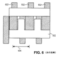
さらに、Dongらは、タイトルが「The Short Winding Path Coupled Inductor Voltage Regulators」の論文において、結合インダクタを提案する。図5は、このDongの論文の多相結合インダクタを表す、1つの結合インダクタ500の上平面図を示す。コア502をより明確に示すために、図5には、巻線は示されていない。しかしながら、図6は、巻線602を含むインダクタ500を示す。
In addition, Dong et al. Propose a coupled inductor in a paper titled “The Short Winding Path Coupled Inductor Voltage Regulators”. FIG. 5 shows a top plan view of one coupled
コア502は、各相の個別の脚504を含む。各脚504は、幅508を有し、隣接する脚504は、幅510を有する窓506によって分離される。したがって、巻線602は、図6および図7に示されるように、間隔幅604を有する。窓幅510は、比較的大きく、およそ脚幅508である。漏れインダクタンスが十分に大きくなるように磁束に経路を提供するために必要とされる、漏れ部分512のための空間を提供するために、大きい窓幅510が必要である。漏れインダクタンスは、漏れ部分512の寸法および/または形状を変更することによって、変化させられ、これは、コア502の寸法および/または形状を変化させる必要がある場合がある。窓506はまた、図6に示されるように、個別の巻線タブも収容する。
Core 502 includes
図7は、図5の線A−Aに沿った、インダクタ500の断面図を示す。各領域702は、個別の脚504の領域に対応し、各領域704は、個別の漏れ部分512の領域に対応する。図7では、巻線602の厚さは、図示上の明瞭さのために誇張されている。図5〜図7から分かるように、漏れ部分512を介して漏れインダクタンスを制御するために、巻線602間に大きい空間が必要である。
FIG. 7 shows a cross-sectional view of the
実施形態では、M−巻線結合インダクタは、第1の端部磁気要素と、第2の端部磁気要素と、M個の接続磁気要素と、M個の巻線とを含む。Mは、1より大きい整数である。各接続磁気要素は、第1の端部磁気要素と第2の端部磁気要素との間に配置され、それらを接続する。各巻線は、M個の接続磁気要素のうちの個別の1つに少なくとも部分的に巻き付けられる。結合インダクタはさらに、磁束に第1の端部磁気要素と第2の端部磁気要素との間の経路を提供するように、M個の接続磁気要素のうちの少なくとも2つに隣接し、それらに少なくとも部分的にわたって延在する、少なくとも1つの上部磁気要素を含む。 In an embodiment, the M-winding coupled inductor includes a first end magnetic element, a second end magnetic element, M connecting magnetic elements, and M windings. M is an integer greater than 1. Each connecting magnetic element is disposed between and connects the first end magnetic element and the second end magnetic element. Each winding is at least partially wound around a separate one of the M connecting magnetic elements. The coupled inductor is further adjacent to at least two of the M connecting magnetic elements to provide a path for the magnetic flux between the first end magnetic element and the second end magnetic element, and Includes at least one upper magnetic element extending at least partially.
実施形態では、M相電源は、結合インダクタと、M個のスイッチング回路とを含む。Mは、1より大きい整数である。結合インダクタは、第1の端部磁気要素と、第2の端部磁気要素と、M個の接続磁気要素と、M個の巻線とを含む。各接続磁気要素は、第1の端部磁気要素と第2の端部磁気要素との間に配置され、それらを接続する。各巻線は、M個の接続磁気要素のうちの個別の1つに少なくとも部分的に巻き付けられる。各巻線は、個別の第1の端部と、個別の第2の端部とを有し、各第1の端部は、共通の第1の節点に電気的に結合される。結合インダクタはさらに、磁束に第1の端部磁気要素と第2の端部磁気要素との間の経路を提供するように、M個の接続磁気要素のうちの少なくとも2つに隣接し、それらに少なくとも部分的にわたって延在する、少なくとも1つの上部磁気要素を含む。各スイッチング回路は、個別の巻線の第2の端部に電気的に結合され、少なくとも2つの異なる電圧間で第2の端部を切り替えるように構成される。
本願明細書は、例えば、以下の項目も提供する。
(項目1)
M−巻線結合インダクタであって、Mは、1より大きい整数であり、該結合インダクタは、
第1の端部磁気要素と、
第2の端部磁気要素と、
M個の接続磁気要素であって、各接続磁気要素は、該第1の端部磁気要素と該第2の端部磁気要素との間に配置され、それらを接続する、M個の接続磁気要素と、
M個の巻線であって、各巻線は、該M個の接続磁気要素のうちの個別の1つに少なくとも部分的に巻き付けられる、M個の巻線と、
磁束に該第1の端部磁気要素と該第2の端部磁気要素との間の経路を提供するように、該M個の接続磁気要素のうちの少なくとも2つに隣接し、それらに少なくとも部分的にわたって延在する、少なくとも1つの上部磁気要素と
を備える、結合インダクタ。
(項目2)
前記少なくとも1つの上部磁気要素は、第1の空隙によって前記第1の端部磁気要素から離間され、該少なくとも1つの上部磁気要素は、第2の空隙によって前記第2の端部磁気要素から離間され、該第1および第2の空隙のそれぞれは、前記磁気要素を形成する1つ以上の磁性材料より低い透磁率を有する個別の空隙材料を含む、項目1に記載の結合インダクタ。
(項目3)
各巻線は、前記第1の空隙の厚さの関数であり、かつ前記第2の空隙の厚さの関数である、個別の漏れインダクタンス値を有する、項目2に記載の結合インダクタ。
(項目4)
接着剤および非磁性スペーサから成る群より選択される非磁性材料をさらに備え、該非磁性材料は、前記少なくとも1つの上部磁気要素を前記第1および第2の端部磁気要素から分離する、項目3に記載の結合インダクタ。
(項目5)
前記M個の巻線のうちの少なくとも1つは、前記少なくとも1つの上部磁気要素と前記第1および第2の端部磁気要素との間のスペーサとしての役割を果たす、項目3に記載の結合インダクタ。
(項目6)
前記少なくとも1つの上部磁気要素は、空隙材料を含む空隙を形成し、前記空隙材料は、前記磁気要素を形成する1つ以上の磁性材料より低い透磁率を有する、項目1に記載の結合インダクタ。
(項目7)
各巻線は、前記空隙の厚さの関数である、個別の漏れインダクタンス値を有する、項目6に記載の結合インダクタ。
(項目8)
Mは、2より大きい整数である、項目7に記載の結合インダクタ。
(項目9)
前記第1および第2の端部磁気要素のうちの少なくとも1つは、前記少なくとも1つの上部磁気要素に隣接する開口部を形成する、項目8に記載の結合インダクタ。
(項目10)
前記少なくとも1つの上部磁気要素は、第1および第2の上部磁気要素を備え、該第1および第2の上部磁気要素は、それらの間に空隙を形成する、項目1に記載の結合インダクタ。
(項目11)
前記少なくとも1つの上部磁気要素は、単一の上部磁気要素を備える、項目1に記載の結合インダクタ。
(項目12)
各巻線は、単層であり、長方形の断面を有する単巻の巻線である、項目1に記載の結合インダクタ。
(項目13)
前記少なくとも1つの上部磁気要素は、外面を形成し、前記外面の少なくとも一部分は、平面である、項目1に記載の結合インダクタ。
(項目14)
各接続磁気要素は、個別の幅を有し、隣接する接続磁気要素は、いずれかの隣接する接続磁気要素の前記個別の幅の25%未満である分離距離で分離される、項目1に記載の結合インダクタ。
(項目15)
各接続磁気要素は、個別の幅を有し、隣接する接続磁気要素は、いずれかの隣接する接続磁気要素の前記個別の幅の10%未満である分離距離で分離される、項目1に記載の結合インダクタ。
(項目16)
前記少なくとも1つの上部磁気要素は、前記M個の接続磁気要素の全てに隣接し、それらにわたって延在する、項目1に記載の結合インダクタ。
(項目17)
前記少なくとも1つの上部磁気要素は、前記M個の接続磁気要素の全て未満に隣接し、それらにわたって延在する、項目1に記載の結合インダクタ。
(項目18)
前記第1および第2の端部磁気要素のうちの少なくとも1つは、前記少なくとも1つの上部磁気要素に隣接する開口部を形成する、項目17に記載の結合インダクタ。
(項目19)
M相電源であって、Mは、1より大きい整数であり、該電源は、
結合インダクタであって、
第1の端部磁気要素と、
第2の端部磁気要素と、
M個の接続磁気要素であって、各接続磁気要素は、該第1の端部磁気要素と該第2の端部磁気要素との間に配置され、それらを接続する、M個の接続磁気要素と、
M個の巻線であって、各巻線は、該M個の接続磁気要素のうちの個別の1つに少なくとも部分的に巻き付けられ、各巻線は、個別の第1の端部と、個別の第2の端部とを有し、各第1の端部は、共通の第1の節点に電気的に結合される、M個の巻線と、
磁束に該第1の端部磁気要素と該第2の端部磁気要素との間の経路を提供するように、該M個の接続磁気要素のうちの少なくとも2つに隣接し、それらに少なくとも部分的にわたって延在する、少なくとも1つの上部磁気要素と
を含む、結合インダクタと、
M個のスイッチング回路であって、各スイッチング回路は、個別の巻線の該第2の端部に電気的に結合され、少なくとも2つの異なる電圧間で該第2の端部を切り替えるように構成される、M個のスイッチング回路と
を備える、M相電源。
(項目20)
Mは、2より大きい整数である、項目19に記載の電源。
(項目21)
前記少なくとも1つの上部磁気要素は、第1の空隙によって前記第1の端部磁気要素から分離され、該少なくとも1つの上部磁気要素は、第2の空隙によって前記第2の磁気要素から分離され、該第1および第2の空隙のそれぞれは、前記磁気要素を形成する1つ以上の磁性材料より低い透磁率を有する個別の空隙材料を含み、各巻線は、該第1の空隙の厚さの関数であり、かつ第2の空隙の厚さの関数である、個別の漏れインダクタンス値を有する、項目19に記載の電源。
(項目22)
前記少なくとも1つの上部磁気要素は、前記磁気要素を形成する1つ以上の磁性材料より低い透磁率を有する空隙材料を含む空隙を形成し、各巻線は、前記空隙の厚さの関数である、個別の漏れインダクタンス値を有する、項目19に記載の電源。
(項目23)
各接続磁気要素は、個別の幅を有し、隣接する接続磁気要素は、いずれかの隣接する接続磁気要素の該個別の幅の25%未満である分離距離で分離される、項目19に記載の電源。
(項目24)
各スイッチング回路は、その個別の第2の端部を、少なくとも20キロヘルツの周波数で、少なくとも2つの異なる電圧間で切り替えるように構成される、項目19に記載の電源。
(項目25)
前記電源は、降圧コンバータ、昇圧コンバータ、および降圧−昇圧コンバータから成る群より選択されるDC−DCコンバータとして動作するように構成される、項目19に記載の電源。
In the embodiment, the M-phase power supply includes a coupled inductor and M switching circuits. M is an integer greater than 1. The coupled inductor includes a first end magnetic element, a second end magnetic element, M connecting magnetic elements, and M windings. Each connecting magnetic element is disposed between and connects the first end magnetic element and the second end magnetic element. Each winding is at least partially wound around a separate one of the M connecting magnetic elements. Each winding has a separate first end and a separate second end, and each first end is electrically coupled to a common first node. The coupled inductor is further adjacent to at least two of the M connecting magnetic elements to provide a path for the magnetic flux between the first end magnetic element and the second end magnetic element, and Includes at least one upper magnetic element extending at least partially. Each switching circuit is electrically coupled to the second end of the individual winding and is configured to switch the second end between at least two different voltages.
This specification provides the following items, for example.
(Item 1)
An M-winding coupled inductor, where M is an integer greater than 1, and the coupled inductor is:
A first end magnetic element;
A second end magnetic element;
M connecting magnetic elements, each connecting magnetic element being disposed between and connecting the first end magnetic element and the second end magnetic element Elements and
M windings, each winding wound at least partially around a separate one of the M connecting magnetic elements;
Adjacent to and at least two of the M connecting magnetic elements to provide a magnetic flux path between the first end magnetic element and the second end magnetic element At least one upper magnetic element extending partially
A coupled inductor comprising:
(Item 2)
The at least one upper magnetic element is separated from the first end magnetic element by a first air gap, and the at least one upper magnetic element is separated from the second end magnetic element by a second air gap. The coupled inductor of
(Item 3)
(Item 4)
(Item 5)
(Item 6)
The coupled inductor of
(Item 7)
(Item 8)
Item 8. The coupled inductor according to
(Item 9)
9. The coupled inductor of item 8, wherein at least one of the first and second end magnetic elements forms an opening adjacent to the at least one upper magnetic element.
(Item 10)
The coupled inductor of
(Item 11)
The coupled inductor of
(Item 12)
(Item 13)
The coupled inductor of
(Item 14)
(Item 15)
(Item 16)
The coupled inductor of
(Item 17)
The coupled inductor of
(Item 18)
The coupled inductor of claim 17, wherein at least one of the first and second end magnetic elements forms an opening adjacent to the at least one upper magnetic element.
(Item 19)
An M-phase power supply, where M is an integer greater than 1;
A coupled inductor,
A first end magnetic element;
A second end magnetic element;
M connecting magnetic elements, each connecting magnetic element being disposed between and connecting the first end magnetic element and the second end magnetic element Elements and
M windings, each winding at least partially wrapped around a separate one of the M connecting magnetic elements, each winding having a separate first end and a separate M windings, each having a second end, wherein each first end is electrically coupled to a common first node;
Adjacent to and at least two of the M connecting magnetic elements to provide a magnetic flux path between the first end magnetic element and the second end magnetic element At least one upper magnetic element extending partially
A coupled inductor comprising:
M switching circuits, each switching circuit being electrically coupled to the second end of a separate winding and configured to switch the second end between at least two different voltages M switching circuits
An M-phase power supply.
(Item 20)
Item 20. The power source of
(Item 21)
The at least one upper magnetic element is separated from the first end magnetic element by a first air gap, and the at least one upper magnetic element is separated from the second magnetic element by a second air gap; Each of the first and second air gaps includes a separate air gap material having a lower permeability than the one or more magnetic materials forming the magnetic element, and each winding has a thickness of the first air gap. Item 20. The power source of
(Item 22)
The at least one upper magnetic element forms a void that includes a void material having a lower permeability than the one or more magnetic materials forming the magnetic element, each winding being a function of the thickness of the void; Item 20. A power source according to
(Item 23)
Item 20. The connection magnetic element has an individual width, and adjacent connection magnetic elements are separated by a separation distance that is less than 25% of the individual width of any adjacent connection magnetic element. Power.
(Item 24)
Item 20. The power supply of
(Item 25)
Item 20. The power supply of
図示における明瞭さのために、図面中の特定の要素は、一定の縮尺で描写されていない場合があることが留意される。アイテムの特定のインスタンスは、丸括弧内の数値の使用によって参照される場合があり(例えば、巻線904(1))、一方、丸括弧のない数字は、任意のそのようなアイテムを指す(例えば、巻線904)。 It is noted that for clarity of illustration, certain elements in the drawings may not be drawn to scale. A particular instance of an item may be referenced by the use of numbers in parentheses (eg, winding 904 (1)), while numbers without parentheses refer to any such item ( For example, winding 904).
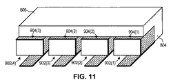
図8は、1つのM−巻線結合インダクタ800の側面斜視図を示す。Mが4と等しい、結合インダクタ800が示されている。しかしながら、Mは、任意の1より大きい整数であってもよい。結合インダクタ800は、それぞれが磁性材料(例えば、フェライト材料および/または粉末鉄材料)で形成される、第1の端部磁気要素802と、第2の端部磁気要素804と、上部磁気要素806とを含む。第1および第2の端部磁気要素802、804は、例えば、相互に対して平行である。第2の端部磁気要素804および上部磁気要素806は、単一の磁気要素に組み合わせられたものとして示されているが、これらの磁気要素は、別個の磁気要素であってもよい。いくつかの実施形態では、上部磁気要素806は、少なくとも実質的に平面的な表面814を形成し、これは、インダクタ800の上面にステッカを必要とすることなく、結合インダクタ800の自動定置を容易にすることができる。
FIG. 8 shows a side perspective view of one M-winding coupled
上部磁気要素806は、磁束に第1の端部磁気要素802と第2の端部磁気要素804との間を移動するための経路を提供する。したがって、上部磁気要素806は、インダクタ800の巻線の漏れインダクタンス値に寄与する、漏れ磁束に経路を提供する。上部磁気要素806はまた、厚さ810を有する空隙808も形成する。空隙808は、結合インダクタ800の長さ812全体に沿って延在するように示されているが、空隙808は、非線形漏れインダクタンス値が望ましい場合等、長さ812の一部分に沿ってのみ延在するように構成することができる。
The top
図9は、接続磁気要素902および巻線904を示すために、第2の端部磁気要素804および上部磁気要素806が除去された、結合インダクタ800の側面斜視図を示す。結合インダクタ800は、磁性材料で形成され、第1の端部磁気要素802と第2の端部磁気要素804との間に配置され、それらを接続する、M個の接続磁気要素902を含む。したがって、上部磁気要素806は、接続磁気要素902のそれぞれに隣接し、それらに少なくとも部分的にわたって延在する。個別の巻線904(斜交平行線で示される)は、M個の接続磁気要素902のうちの個別の1つに少なくとも部分的に巻き付けられる。図10は、接続磁気要素902をより良く示すために、第2の端部磁気要素804、上部磁気要素806、および巻線904が除去された、結合インダクタ800の側面斜視図を示す。各接続磁気要素902は、個別の幅1002を有する。接続磁気要素902は、長方形であり、等幅1002を有するように示されているが、それらの形状は、変化させる(例えば、円形)ことができ、接続磁気要素902の各インスタンスは、同一幅1002を有する必要はない。
FIG. 9 shows a side perspective view of the coupled
空隙808は、第1の端部磁気要素802、第2の端部磁気要素804、上部磁気要素806、および接続磁気要素902を形成する、1つ以上の磁性材料より低い透磁率を有する材料を含む(例えば、それで少なくとも部分的に充填される)。例えば、空隙808は、空気、絶縁テープ、プラスチック、接着剤、および/または紙等の非磁性材料を含むことができる。別の実施例として、空隙808は任意に、巻線904が非線形漏れインダクタンス値を有するように、結合インダクタ800の予測される通常の動作中に飽和する、可飽和磁性材料を含むことができる。上部磁気要素806および空隙808は典型的に、各巻線904の個別の漏れインダクタンスの最重要寄与要因である。したがって、漏れインダクタンスは、空隙808の厚さ810を変化させることによって変化させることができ、漏れインダクタンスは、厚さ810に比例して増加する。
The
図11は、インダクタ800を図8〜図10とは反対の側面斜視から示す。図11では、第1の端部磁気要素802が除去されている。図12は、結合インダクタ800の上平面図であり、点線は、磁気要素によって覆い隠されている、巻線904の輪郭を示す。巻線904は、回路基板配線長さを最小化し、DC−DCコンバータ電力密度を最大化するように、例えば、結合インダクタ800が取り付けられるDC−DCコンバータの電力段の間隔幅と等しい間隔幅1202を有する。間隔幅1202は、巻線904の各対について同一であるように示されているが、間隔幅1202は、電力段幾何学形状を収容するため等、巻線の対の間で異なってもよい。
FIG. 11 shows the
図13は、図12の線B−Bに沿って切り取った、インダクタ800の断面図を示す。領域1302は、個別の幅1306を有する窓1304によって分離される、接続磁気要素902の領域を表す。領域1308は、上部磁気要素806の断面を表す。図13では、巻線904の厚さは、図示上の明瞭さのために誇張されている。各窓1304は、必ずしも同一の幅1306を有する必要はない。接続磁気要素902は、漏れ部分のための空間を提供して漏れインダクタンスを上昇させるために分離されている必要はないため、窓幅1306は、小さくすることができる。代わりに、上述されるように、漏れインダクタンスは主として、上部磁気要素806および空隙808によって生じる。実際、窓幅1306は、巻線904が短絡するのを防止するのに辛うじて十分に大きい等、可能な限り小さくすることができる。例えば、いくつかの実施形態では、窓幅1306は、接続磁気要素幅1002の50%、25%、または10%未満である。したがって、いくつかの実施形態では、隣接する接続磁気要素902は、いずれかの隣接する接続磁気要素の個別の幅1002の50%、25%、または10%未満である分離距離(すなわち、窓幅1306)で分離される。窓幅1306が比較的小さくなるように結合インダクタ800を構成することによって、以下に記載されるように、結合インダクタ800の、巻線を共に磁気結合するために利用される体積の部分が有利に増加される。
FIG. 13 shows a cross-sectional view of
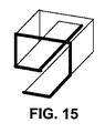
巻線904は、巻線インピーダンスを最小化するのを助長するように、例えば、単巻、少なくとも実質的に長方形の断面を有する単層巻線である。図14は、1つの巻線904の側面斜視図を示し、図15は、1つの巻線904の部分透視図を示す。巻線904はしかしながら、他の構成を有することができる。例えば、図16〜図18は、他の可能な巻線構成の実施例を示す。別の実施例として、図19は、結合インダクタ800の三巻線実施形態である、1つの結合インダクタ1900の上平面図を示す。結合インダクタ1900は、例えば、導電性材料(例えば、銅)の長方形シートから形成される、巻線1902を含む。図19の上平面図では見えない巻線1902の縁部の輪郭は、点線で描かれている。さらに、図19の上平面図では覆い隠されている接続磁気要素の縁部もまた、点線で示されている。
Winding 904 is, for example, a single turn, a single layer winding having at least a substantially rectangular cross-section to help minimize winding impedance. FIG. 14 shows a side perspective view of one winding 904, and FIG. 15 shows a partial perspective view of one winding 904. Winding 904 can, however, have other configurations. For example, FIGS. 16-18 show examples of other possible winding configurations. As another example, FIG. 19 shows a top plan view of one coupled
各巻線904は、インダクタ800の側1204および1206(図12を参照)のそれぞれから延在する端部を有するように示されているが、巻線904は、インダクタ800から異なるように延在することができる、または全く延在しなくてもよい。例えば、1つ以上の巻線904の各端部は、電力段レイアウト要件に適合するため等、インダクタ800の共通の側から延在することができる。さらに、巻線904は、貫通孔ピンを含むように、またはそれに結合されるように修正することができる。
Each winding 904 is shown as having an end extending from each of the
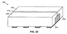
上部磁気要素806の構成は、変化させることができる。例えば、上部磁気要素806は、図20に示されるもの等、2つ以上の上部磁気要素で置換することができる。具体的に、図20は、結合インダクタ800の代替の実施形態である、1つの結合インダクタ2000の側面斜視図を示す。結合インダクタ2000では、第1の上部磁気要素2002は、第1の端部磁気要素2004から接続磁気要素にわたって延在し、第2の上部磁気要素2006は、第2の端部磁気要素2008から接続磁気要素にわたって延在する。上部磁気要素2002、2006は、空隙2010を形成する。
The configuration of the upper
Mが比較的大きい、結合インダクタ800の実施形態では、インダクタ800の長さ812は、M個の接続磁気要素902のそれぞれを収容するように、比較的長くなる。インダクタ800のそのような比較的長い長さ812は、厚さ810に対して直交する空隙808の断面積を増加させ、それによって、巻線904の漏れインダクタンス値を増加させる。漏れインダクタンスが望ましくないほど大きい場合、これは、空隙808の厚さ810を増加させることによって低減することができる。
したがって、所望の漏れインダクタンスを維持するために、巻線の数が増加するにつれて、空隙808の厚さ810が増加される場合がある。
In an embodiment of a coupled
Accordingly, the
上部磁気要素806、第1の端部磁気要素802、および/または第2の端部磁気要素804の構成もまた、巻線漏れインダクタンス値を決定するように変化させることができる。例えば、巻線が増加される際、所望の空隙断面積を維持する(およびそれによって所望の漏れインダクタンス値を維持する)ために、磁気要素806に隣接する端部磁気要素802、804のうちの1つ以上内に開口部を形成することができる。図21〜図24は、そのような技術の一実施例を示す。
The configuration of the top
図21は、結合インダクタ800の二巻線実施形態である、1つの結合インダクタ2100の側面斜視図を示す。結合インダクタ2100は、空隙2108を形成する、第1の端部磁気要素2102と、第2の端部磁気要素2104と、上部磁気要素2106とを含む。空隙2108は、インダクタの巻線の漏れインダクタンス値を主として決定する、厚さ2110を有する。
FIG. 21 shows a side perspective view of one coupled
図22は、結合インダクタ800の三巻線の代替の実施形態である、1つの結合インダクタ2200の側面斜視図を示す。結合インダクタ2200は、第1の端部磁気要素2202と、第2の端部磁気要素2204と、上部磁気要素2206とを含む。第1の端部磁気要素2202は、開口部2208を形成し、これは、それぞれが、インダクタ2100の空隙2108の厚さ2110(図21)と同一である個別の厚さ2212を有する、2つの空隙2210を形成する、上部磁気要素2206をもたらす。開口部2208の寸法は、両方の空隙2210のそれらの厚さ2212に対して直交する集合的断面積が、インダクタ2100の空隙2108のその厚さ2110に対して直交する断面積と略同一となるように選択される。したがって、結合インダクタ2200は、インダクタ2200が、インダクタ2100より多くの巻線、およびインダクタ2100と同一の空隙厚さを有するにも関わらず、インダクタ2100と略同一の巻線漏れインダクタンス値を有する。
FIG. 22 shows a side perspective view of one coupled
図23は、第1の端部磁気要素2302と、第2の端部磁気要素2304と、上部磁気要素2306とを含む、結合インダクタ800の四巻線の代替の実施形態である、1つの結合インダクタ2300の側面斜視図を示す。結合インダクタ2300は、結合インダクタ2200(図22)と類似する。しかしながら、結合インダクタ2300は、4つの巻線を含み、第1の端部磁気要素2302内に形成される開口部2308の寸法は、空隙2310のそれらの厚さ2312に対して直交する集合的断面積が、インダクタ2100の空隙2108のその厚さ2110(図21)に対して直交する断面積と略同一となるように選択される。各空隙2310の厚さ2312は、インダクタ2100の空隙2108の厚さ2110と同一である。したがって、結合インダクタ2300は、結合インダクタ2300が、インダクタ2100および2200より多くの巻線、ならびにインダクタ2100および2200と同一の空隙厚さを有するにも関わらず、結合インダクタ2100および2200と略同一の巻線漏れインダクタンス値を有する。
FIG. 23 is an illustration of an alternative embodiment of a four winding of a coupled
図24は、第2の端部磁気要素2304および上部磁気要素2306が除去された、インダクタ2300の側面斜視図を示す。図24では、接続磁気要素2402および巻線2404を見ることができる。
FIG. 24 shows a side perspective view of the
したがって、図21〜図24から示されるように、巻線の数が増加される際、上部磁気要素に隣接する端部磁気要素内に開口部を追加することによって、漏れインダクタンスを所望の値に維持することができ、開口部寸法は、全ての空隙の所望の総断面積を達成し、それによって、所望の巻線漏れインダクタンスを達成するように選択される。大きい数の巻線を有する実施形態では、一部の磁束が開口部を通って移動するため、開口部寸法は典型的に、所望の空隙断面積を達成するために必要とされるよりわずかに大きい。 Thus, as shown in FIGS. 21-24, when the number of windings is increased, the leakage inductance is brought to a desired value by adding an opening in the end magnetic element adjacent to the upper magnetic element. The aperture size can be maintained and is selected to achieve the desired total cross-sectional area of all air gaps, thereby achieving the desired winding leakage inductance. In embodiments with a large number of windings, the opening dimension is typically slightly less than needed to achieve the desired gap cross-sectional area because some magnetic flux moves through the opening. large.
巻線の数が増加される際、上部磁気要素806の構成もまた、所望の空隙断面積を維持する(およびそれによって所望の巻線漏れインダクタンス値を維持する)ように変化させることができる。図25〜図30は、そのような技術の一実施例を示す。
As the number of windings is increased, the configuration of the top
図25は、結合インダクタ800(図8)の二巻線の代替の実施形態である、1つの結合インダクタ2500の側面斜視図を示す。図26は、結合インダクタ2500の側平面図を示す。結合インダクタ2500は、空隙2508を形成する、第1の端部磁気要素2502と、第2の端部磁気要素2504と、上部磁気要素2506とを含む。インダクタ2500の製造中に空隙2508を制御することを容易にするために、任意に、非磁性材料で形成されるもの等のスペーサ(図示せず)を空隙2508内に含むことができる。空隙2508は、結合インダクタ2500の全長2510に及び、空隙2508は、厚さ2602(図26を参照)を有する。上外面2512の全体は、インダクタ2500の上面にステッカを必要とすることなく、結合インダクタ2500の自動定置を容易にするように、例えば、少なくとも実質的に平面である。
FIG. 25 shows a side perspective view of one coupled
図27は、結合インダクタ2500の三巻線の代替の実施形態である、1つの結合インダクタ2700の側面斜視図を示し、図28は、その側平面図を示す。結合インダクタ2700は、空隙2508の厚さ2602と同一である厚さ2802を有する空隙2804(図28を参照)を形成する、第1の端部磁気要素2702と、第2の端部磁気要素2704と、上部磁気要素2706とを含む。しかしながら、結合インダクタ2500とは対照的に、空隙2804は、インダクタ2700の全長2710には及ばない。代わりに、上部磁気要素2706は、空隙2804のその厚さ2802に対して直交する断面積が、インダクタ2500の空隙2508のその厚さ2602に対して直交する断面積と略同一となるように構成される。したがって、インダクタ2700の巻線漏れインダクタンス値は、インダクタ2700が、インダクタ2500より多くの巻線、およびインダクタ2500と同一の空隙厚さを有するにも関わらず、インダクタ2500と略同一である。
FIG. 27 shows a side perspective view of one coupled
図29は、結合インダクタ2500の四巻線の代替の実施形態である、1つの結合インダクタ2900の側面斜視図を示し、図30は、その側平面図を示す。結合インダクタ2900は、空隙2508の厚さ2602と同一である厚さ3002を有する空隙3004(図30を参照)を形成する、第1の端部磁気要素2902と、第2の端部磁気要素2904と、上部磁気要素2906とを含む。インダクタ2700(図27)と同様に、上部磁気要素2906は、空隙3004のその厚さ3002に対して直交する断面積が、インダクタ2500の空隙2508(図25)のその厚さ2602に対して直交する断面積と略同一となるように構成される。したがって、インダクタ2900の巻線漏れインダクタンス値は、インダクタ2900が、インダクタ2500および2700より多くの巻線、ならびにインダクタ2500および2700と同一の空隙厚さを有するにも関わらず、インダクタ2500および2700と略同一である。
FIG. 29 shows a side perspective view of one coupled
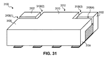
図31は、結合インダクタ800(図8)の代替の実施形態であり、結合インダクタ2300(図23)および結合インダクタ2900(図29)の両方のいくつかの特徴を含む、1つの結合インダクタ3100の側面斜視図を示す。結合インダクタ3100は、磁束に第1の端部磁気要素3102と第2の端部磁気要素3104との間を移動するための経路を提供する、第1の端部磁気要素3102と、第2の端部磁気要素3104と、上部磁気要素3106とを含む。上部磁気要素3106はさらに、空隙3108を形成する。上部磁気要素3106は、第1の端部磁気要素3102内の開口部3112に延在するが、第1の端部磁気要素3102と接触しない、延在部3110を形成する。図32は、インダクタ3100を図31とは反対の側面斜視から示す。空隙3108の比較的大きい集合的断面積のため、インダクタ3100の巻線漏れインダクタンス値は、比較的大きい場合がある。しかしながら、インダクタ3100の大きい数の空隙3108は、巻線漏れインダクタンス値の決定における十分な柔軟性を提供することができる。
FIG. 31 is an alternative embodiment of a coupled inductor 800 (FIG. 8), including one feature of both coupled inductor 2300 (FIG. 23) and coupled inductor 2900 (FIG. 29). A side perspective view is shown. The coupled
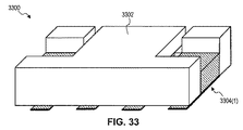
図33は、結合インダクタ3100(図33)の代替の実施形態である、1つの結合インダクタ3300の側面斜視図である。結合インダクタ3300は、結合インダクタ3100と類似する。しかしながら、結合インダクタ3100とは対照的に、結合インダクタ3300の上部磁気要素3302は、全ての接続磁気要素3304にわたって延在せず、それによって、空隙断面積を減少させる。したがって、結合インダクタ3300は一般的に、結合インダクタ3100の実施形態より小さい漏れインダクタンス値を有する。
FIG. 33 is a side perspective view of one coupled
結合インダクタ800は、他の結合インダクタより優れた、多数の潜在的利点を有することができる。1つの潜在的利点は、結合インダクタ800が、同様のインダクタンスおよび電流付加耐量特性を伴う他の結合インダクタより小さい設置面積を有することができるということである。具体的に、漏れインダクタンスは主として、上部要素806および空隙808を介して生じ、制御される。その結果、典型的にインダクタ設置面積寸法を増加させる、漏れインダクタンスを増加させるための他の特徴が必要とされない。例えば、他の結合インダクタにおいて漏れインダクタンス値を増加させるために使用される、インダクタの端部または巻線間の漏れ部分(例えば、図5〜図7のインダクタ500を参照)に追加される、空隙を伴う外脚は、結合インダクタ800では必要とされない。
The coupled
さらに、上述されるように、漏れインダクタンスは、空隙808の厚さ810を変化させることによって調整可能である。したがって、漏れインダクタンスは、単に上部磁気要素806を細かくすることによって等、容易に調整することができる。対照的に、結合インダクタ100(図1〜図3)または結合インダクタ500(図5〜図7)の漏れインダクタンスを調整するためには、コア幾何学形状および/または漏れ部分が変更されなければならない。
Further, as described above, the leakage inductance can be adjusted by changing the
さらに、結合インダクタ800は、巻線間に幅広の窓幅1306を有する必要がなく、それによって、コア断面の巻線を磁気結合するのに利用可能な部分を最大化することを助長する。例えば、図13では、巻線904を共に結合する磁性材料が断面の大部分を占め、窓1304のみが磁性材料を含まない。したがって、インダクタ800は、同様の巻線間隔幅を伴う他のインダクタより大きい磁化インダクタンスを有することができ、これは、巻線間の磁気結合を高め、巻線の間の漏れインダクタンスおよび磁化インダクタンスの均一性を高め、巻線電流不整合による飽和に対する耐性を高め、および/またはコア損失を低減する。さらに、結合インダクタ800のいくつかの実施形態によって提供される、大きい磁気結合は、より低い透磁率のコア材料を使用することを可能にし、それによって、コア損失を低減することができる。
Further, the coupled
対照的に、結合インダクタ100(図1〜図3)または結合インダクタ500(図5〜図7)等のいくつかの他の結合インダクタでは、インダクタの体積の相当部分が巻線を共に磁気結合するために利用されない。そのような事実は、図7および図13を比較することによって理解することができ、結合インダクタ800は、同一の巻線間隔幅で、結合インダクタ500より著しく多い、巻線を共に結合する磁気コア材料を含む。
In contrast, in some other coupled inductors, such as coupled inductor 100 (FIGS. 1-3) or coupled inductor 500 (FIGS. 5-7), a substantial portion of the inductor volume magnetically couples the windings together. Not used for. Such a fact can be understood by comparing FIGS. 7 and 13, where the coupled
さらに、結合インダクタ800の特定の実施形態は、巻線904が短い長さおよび広い幅を有することを可能にし、それによって、巻線抵抗および関連電力損失を低減する。対照的に、いくつかの先行技術の結合インダクタは、例えば、結合インダクタ100の巻線104の長さ(図4を参照)によって示されるような、大幅に長い巻線を必要とする。
Furthermore, certain embodiments of the coupled
さらに、結合インダクタ800のいくかの実施形態は、薄い磁気コア片を必要とせず、それによって、機械的強度を促進し、製造、輸送、取り扱い、および/または組み立てを容易にする。対照的に、いくつかの他の結合インダクタは、脆弱な薄いコア片を必要とし、製造、輸送、取り扱い、および/または組み立てが困難である。例えば、結合インダクタ100のコア102(図1)は、薄い上部片および薄い下部片を必要とする場合がある。
Further, some embodiments of the coupled
図34は、1つのM−巻線結合インダクタ3400の上面斜視図を示す。Mが4である、結合インダクタ3400が示されている。しかしながら、Mは、任意の1より大きい整数であってもよい。結合インダクタ3400は、結合インダクタ800と類似するが、その主要漏れ磁束経路と直列の2つの空隙を含む。具体的に、結合インダクタ3400は、第1の端部磁気要素3404および第2の端部磁気要素3406を含む磁気コア3402と、上部磁気要素3408とを含む。第1の空隙3410は、上部磁石要素3408を第1の端部磁気要素3404から分離し、第2の空隙3412は、上部磁気要素3408を第2の端部磁気要素3406から分離する。第1および第2の空隙3410、3412は、それぞれ、磁気コア3402を形成する1つ以上の磁性材料より低い透磁率を有する、個別の空隙材料(例えば、空気、絶縁テープ、プラスチック、接着剤、および/または紙)を含む。上部磁気要素3408は、外面または上面3422を形成し、特定の実施形態では、表面3422の少なくとも一部分は、少なくとも実質的に平面である。
FIG. 34 shows a top perspective view of one M-winding coupled
図35は、上部磁気要素3408が除去された、コア3402の上面斜視図を示す。コア3502は、第1の端部磁気要素3404と第2の端部磁気要素3406との間に配置され、それらを接続する、M個の接続磁気要素3414を含む。したがって、上部磁気要素3408は、接続磁気要素3414のそれぞれに隣接し、それらに少なくとも部分的にわたって延在する。第1および第2の端部磁気要素3404、3406は、例えば、コア3402が梯子形コアを形成するように、相互に対して平行である。コア3402の磁気要素は、コア3402を形成するように接合される別個の磁気要素として示されているが、磁気要素のうちの1つ以上を、単一の磁気要素に組み合わせることができる(例えば、接続磁気要素3414および第1の端部磁気要素3404を、単一の磁気要素に組み合わせることができる)。
FIG. 35 shows a top perspective view of the
結合インダクタ3400はさらに、各接続磁気要素3414に少なくとも部分的に巻き付けられる、個別の巻線3416を含む。図36は、結合インダクタ3400の上面斜視図を示し、磁気コア3402は、巻線3416を示すために、透明なものとして示されている。巻線3416の構成は、図16〜図18の実施例のものと同様のものになるように等、変化させることができる。図37は、結合インダクタ3400の側面3418の図を示す。
The coupled
接着剤、エポキシ、および/または1つ以上の非磁性スペーサ等の非磁性材料3708(図37)は典型的に、上部磁気要素3408を第1および第2の端部磁気要素3404、3406から分離し、それによって第1および第2の空隙3410、3412を生じさせるように、コア3402の上部磁気要素3408と1つ以上の他の要素(例えば、第1および第2の端部磁気要素3404、3406)との間に配置される。磁性スペーサは任意に、粘着剤であり、そのような場合、上部磁石要素3408を第1および第2の端部磁気要素3404、3406に少なくとも部分的に固定する。接着剤はまた、上部磁石要素3408を第1および第2の端部磁気要素3404、3406に少なくとも部分的に固定するために使用することもできる。図38〜図40は、それぞれが上部磁石要素3408を第1および第2の端部磁気要素3404、3406から分離する、1つ以上の非磁性スペーサ3802を含む、結合インダクタ3400の実施形態である、結合インダクタ3800、3900、および4000の上面斜視図をそれぞれ示す。コア3402は、図38〜図40では、非磁性スペーサ3802を示すために、透明なものとして示されている。
Nonmagnetic material 3708 (FIG. 37), such as adhesive, epoxy, and / or one or more nonmagnetic spacers, typically separates the top
特定の代替の実施形態では、結合インダクタの巻線のうちの少なくとも1つは、コアの上部磁気要素と1つ以上の他の要素との間のスペーサとしての役割を果たす。例えば、図41は、結合インダクタ3400の代替の実施形態である、結合インダクタ4100の側面図を示し、巻線4102(巻線3416と類似する)は、上部磁気要素4104を第1および第2の端部磁気要素4106、4108から分離するのを助長する。接着剤またはエポキシ等の粘着性材料(図示せず)は典型的に、上部磁気要素4104を結合インダクタ4100の残りの部分に保持するために使用される。そのような粘着性材料はまた典型的に、上部磁気要素4104を端部磁気要素4106、4108から分離するのも助長する。巻線4102を上部磁気要素4104と端部磁気要素4106、4108との間のスペーサとして使用することによって、空隙厚さ4110、4112を精密に制御することを容易にすることができる。
In certain alternative embodiments, at least one of the windings of the coupled inductor serves as a spacer between the upper magnetic element of the core and one or more other elements. For example, FIG. 41 shows a side view of a coupled
上部磁気要素3408は、磁束に第1の端部磁気要素3404と第2の端部磁気要素3406との間を移動するための経路を提供する。したがって、上部磁気要素3408は、漏れ磁束に経路を提供し、第1および第2の空隙3410、3412は、それぞれ、上部磁気要素3408の漏れ磁束経路と直列である。したがって、上部磁気要素3408ならびに第1および第2の空隙3410、3412は典型的に、各巻線3416の個別の漏れインダクタンスの最重要寄与要因である。したがって、漏れインダクタンスは、空隙第1の空隙3410の厚さ3702および/または第2の空隙3412の厚さ3704(図37を参照)を変化させることによって変化させることができ、漏れインダクタンスは、厚さ3702、3704に比例して増加する。漏れ磁束経路内に2つの空隙3410、3412を含む結合インダクタ3400のため、空隙3410、3412は典型的に、漏れ磁束経路内に単一の空隙しか含まないインダクタの漏れ磁束経路内の空隙より薄い。
The top
厚さ3702、3704は、図37では同一であるように示されているが、厚さ3702は、厚さ3704と同一である必要はない。さらに、第1および第2の空隙3410、3412のそれぞれは、結合インダクタ3400の長さ3420の全体に沿って延在するように示されているが、第1および第2の空隙3410、3412のうちの1つ以上は、長さ3420の部分のみに沿って延在するように修正することができる。さらに、第1および第2の空隙3410、3412のうちの1つ以上は、非線形漏れインダクタンス値を生じさせるため等、結合インダクタ3400の幅3420に沿って、および/または深さ3706に沿って不均一である、厚さ3702、3704を有することができる。さらに、結合インダクタ3400は、上部磁気要素3408の漏れ磁束経路内に、第1および第2の空隙3410、3412に加えて、1つ以上の空隙を含むように修正することができる。
Although the
結合インダクタ3400の特定の実施形態は、同様のインダクタンスおよび電流付加耐量特性を伴う、いくつかの他の結合インダクタより小さい設置面積、漏れインダクタンスを容易に調整する能力、隣接する巻線を近接して定置する能力、ならびに短いおよび/または幅広の巻線を使用する能力等、結合インダクタ800に関して上述されるものと同様の利点を有する。さらに、以下に記載されるように、結合インダクタ3400の特定の実施形態は、結合インダクタ800の特定の実施形態によって必ずしも実現される必要はない、追加の利点を有する。
Certain embodiments of the coupled
例えば、結合インダクタ3400の特定の実施形態では、上面3422の少なくとも一部分には、空隙がなく、実質的に平らであり(空隙3410、3412は、表面3422の側にある)、それによって潜在的に、表面3422上にラベルまたはカバーを使用する必要なく、ピックアンドプレース組み立てを可能にする。ラベルまたはカバーを使用する必要がないことは有利に、材料および人件費を削減すること、結合インダクタ3400の高さ3424を低減すること、および/または上面3422からインダクタの環境への熱の伝達を促進することができる。
For example, in certain embodiments of the coupled
別の実施例として、結合インダクタ3400の特定の実施形態は、多数の単純な形状(例えば、実質的に長方形)の磁気要素から形成されるコアを含み、それによって、低コア費用および製造可能性を促進する。そのような磁気要素は、対称であり、それによって、コア3402を形成するために必要とされる磁気要素の数を削減することができる。例えば、特定の実施形態では、第1および第2の端部磁気要素3404、3406は、交換可能であり、それによって、コア3402を形成するために備蓄される、異なる磁気要素の数を削減する。
As another example, certain embodiments of coupled
さらに別の実施例として、空隙厚さ3702、3704が、第1および第2の端部磁気要素3404、3406に対する上部磁気要素3408の位置によって決定されるという事実は、空隙厚さを比較的容易に制御することを可能にすることができる。例えば、特定の実施形態では、空隙厚さは主として、上部磁気要素3408を第1および第2の端部磁気要素3404、3406から分離する非磁性スペーサならびに/または接着剤の厚さによって制御される。
As yet another example, the fact that the
別の実施例として、単一の空隙の代わりに2つの空隙3410、3412を使用することによって、結合インダクタ3400から放出される浮遊磁界を低減することができる。特に、上述されるように、空隙3410、3412は典型的に、漏れ磁束経路内に単一の空隙しか含まないインダクタの漏れ磁束経路内の空隙より薄い。そのようなより小さい空隙は、浮遊磁界を低減することができ、これは言い換えると、結合インダクタ3400からの電磁干渉を低減することができる。浮遊磁界の低減はまた、浮遊磁界から金属部品内に誘導される電流からもたらされる、隣接する金属部品における損失も低減することができる。
As another example, the stray field emitted from the coupled
本明細書に開示される結合インダクタの1つの考えられる用途は、スイッチングDC−DCコンバータ等の電源である。したがって、本明細書に開示される結合インダクタの磁気コアを形成するために使用される磁性材料は典型的に、スイッチング電源において一般的である高スイッチング周波数(例えば、少なくとも20KHz)で比較的低いコア損失を呈する材料(例えば、フェライト材料または粉末鉄材料)である。 One possible application of the coupled inductor disclosed herein is a power source such as a switching DC-DC converter. Accordingly, the magnetic material used to form the magnetic core of the coupled inductor disclosed herein is typically a relatively low core at high switching frequencies (eg, at least 20 KHz) that are common in switching power supplies. It is a material that exhibits loss (for example, a ferrite material or a powdered iron material).
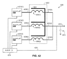
図41は、本明細書に記載される結合インダクタの1つの考えられる用途である、1つの電源4200を図式的に示す。電源4200は、3つの相を有するように示されているが、電源4200は、2つ以上の任意の数の相を有することができる。
FIG. 41 schematically illustrates one
電源4200は、例えば、本明細書に記載される結合インダクタのうちの1つの三巻線実施形態(例えば、結合インダクタ800、1900、2000、2100、2200、2300、2500、2700、2900、3100、3300、3400、または4100のうちの1つの三巻線実施形態)である、結合インダクタ4202を含む。結合インダクタ4202は、磁気コア4204と、3つの巻線4206とを含む。各巻線4206は、共通の第1の節点4212に電気的に結合される、第1の端部4210を有する。各第1の端部4210は任意に、インダクタ4202の1つの共通の側(例えば、図12の側1204)から延在する。各巻線4206はさらに、個別のスイッチング回路4214に電気的に結合される、第2の端部4208を含む。各第2の端部4208は任意に、インダクタ4202の別の共通の側(例えば、図12の側1206)から延在する。巻線4206は、その第2の端部4208から1つの巻線4206を通ってその第1の端部4210に流れる電流が、各他の巻線4206内に、その第2の端部4208からその第1の端部4210に流れる電流を誘導するように、コア4204上に巻かれる。スイッチング回路4214は、それらの個別の巻線4206の第2の端部4208を少なくとも2つの異なる電圧間で切り替えるように構成され、配設される。コントローラ4218は、スイッチング回路4214を制御し、コントローラ4218は任意に、第1の節点4212へ等のフィードバック接続4220を含む。第1の節点4212は任意に、フィルタ4216を含む。
The
電源4200は典型的に、スイッチング電流による構成要素の移動から生じる音が、人が知覚可能な周波数範囲を超えるような、少なくとも約20kHzのスイッチング周波数、スイッチング回路4214が切り替える周波数を有する。スイッチング電源4200を、低スイッチング周波数の代わりに高スイッチング周波数(例えば、少なくとも20kHz)で動作させることによって、また、(1)エネルギー貯蔵構成要素(例えば、結合インダクタ4202およびフィルタコンデンサ)の寸法の低減、(2)リップル電流およびリップル電圧振幅の低減、ならびに/または(3)改善されたコンバータ過渡応答を促進することもできる。高スイッチング周波数での効率的な動作を可能にするために、結合インダクタ4202の磁気コア4204を形成する1つ以上の磁性材料は典型的に、高周波数動作で比較的低いコア損失を有する材料である。
The
いくつかの実施形態では、コントローラ4218は、各スイッチング回路4214が各他のスイッチング回路4214とは異なる相で動作するように、スイッチング回路4214を制御する。換言すれば、そのような実施形態では、各スイッチング回路4214によってその個別の第2の端部4208に提供される、切り替えられた波形は、各他のスイッチング回路4214によってその個別の第2の端部4208に提供される、切り替えられた波形に対して位相シフトされる。例えば、電源4200の特定の実施形態では、スイッチング回路4214(1)は、スイッチング回路4214(2)によって第2の端部4208(2)に提供される、切り替えられた波形、およびスイッチング回路4214(3)によって第2の端部4208(3)に提供される、切り替えられた波形から約120度位相がずれている、切り替えられた波形を第2の端部4208(1)に提供する。
In some embodiments, the
電源4200は、種々の構成を有するように構成し、配設することができる。例えば、電源4200が降圧コンバータとして構成され、第1の節点4212が出力電圧節点であり、フィルタ4216が出力フィルタであるようなスイッチング回路4214は、それらの個別の巻線4206の第2の端部4208を、入力電圧節点(図示せず)とグランドとの間で切り替えることができる。本実施例では、各スイッチング回路4214は、少なくとも1つの高側スイッチングデバイスおよび少なくとも1つのキャッチダイオード、または少なくとも1つの高側スイッチングデバイスおよび少なくとも1つの低側スイッチングデバイスを含む。本文献の文脈では、スイッチングデバイスには、バイポーラ接合トランジスタ、電界効果トランジスタ(例えば、N−チャネルまたはP−チャネル金属酸化膜半導体電界効果トランジスタ、接合型電界効果トランジスタ、金属−半導体電界効果トランジスタ)、絶縁ゲート型バイポーラ接合トランジスタ、サイリスタ、またはシリコン制御整流器が挙げられるが、これらに限定されない。
The
別の実施例として、電源4200は、節点4212が入力電力節点であり、スイッチング回路4214がそれらの個別の巻線4206の第2の端部4208を出力電圧節点(図示せず)とグランドとの間で切り替えるような、昇圧コンバータとして構成することができる。さらに、電源4200は、例えば、節点4212が共通の節点であり、スイッチング回路4214がそれらの個別の巻線4206の第2の端部4208を出力電圧節点(図示せず)と入力電圧節点(図示せず)との間で切り替えるような、降圧−昇圧コンバータとして構成することができる。
As another example,
さらに、さらに別の実施例として、電源4200は、孤立したトポロジを形成することができる。例えば、各スイッチング回路4214は、変圧器と、変圧器の一次巻線に電気的に結合される、少なくとも1つのスイッチングデバイスと、変圧器の二次巻線と個別の巻線4206の第2の端部4208との間に結合される整流回路とを含むことができる。整流回路は任意に、効率を改善するように、少なくとも1つのスイッチングデバイスを含む。
As yet another example, the
電源4200の1つの考えられる用途は、図43のコンピューティング装置4300等のコンピューティング装置である。コンピューティング装置4300は、例えば、個人用コンピュータもしくはサーバのマザーボード、サーバの処理ボード、コンピューティング能力を伴う携帯電話、または個人用デジタル補助装置である。電源4200の実施形態である、電源4302は、プロセッサ4304に少なくとも部分的に電力供給する。電源4302は、例えば、本明細書に記載される結合インダクタのうちの1つの実施形態(例えば、結合インダクタ800、1900、2000、2100、2200、2300、2500、2700、2900、3100、3300、3400、または4100のうちの1つの実施形態)である、結合インダクタ4306を含む。
One possible application of the
上記の方法およびシステムに、その範囲から逸脱することなく、変更を行うことができる。したがって、上述に含まれ、添付の図面中に示される事柄は、制限的な意味ではなく、実例として解釈されるべきであることに留意されたい。以下の特許請求の範囲は、本明細書に記載される、包括的特徴および具体的特徴を網羅すること、ならびに本方法およびシステムの範囲の全ての記述は、言語上の事実として、その範囲内に含まれるということができることが意図される。 Changes can be made to the above methods and systems without departing from the scope thereof. Accordingly, it should be noted that the matter contained above and shown in the accompanying drawings should be interpreted as illustrative rather than restrictive. The following claims are intended to cover the generic and specific features described herein, and all descriptions of the scope of the method and system are within their scope as linguistic facts. It is intended that it can be included.
Claims (21)
第1の端部磁気要素と、
第2の端部磁気要素と、
M個の接続磁気要素であって、各接続磁気要素は、該第1の端部磁気要素と該第2の端部磁気要素との間に配置され、それらを接続する、M個の接続磁気要素と、
M個の巻線であって、各巻線は、該M個の接続磁気要素のうちの個別の1つに少なくとも部分的に巻き付けられる、M個の巻線と、
磁束に該第1の端部磁気要素と該第2の端部磁気要素との間の経路を提供するように、該M個の接続磁気要素のうちの少なくとも2つに隣接し、それらに少なくとも部分的にわたって延在する上部磁気要素と
を備え、
該上部磁気要素は、少なくとも部分的に該第1の端部磁気要素にわたって延在し、かつ、第1の空隙によって該第1の端部磁気要素から離間され、該上部磁気要素は、少なくとも部分的に該第2の端部磁気要素にわたって延在し、かつ、第2の空隙によって該第2の端部磁気要素から離間され、該第1および第2の空隙のそれぞれは、該磁気要素を形成する1つ以上の磁性材料より低い透磁率を有する個別の空隙材料を含む、結合インダクタ。 An M-winding coupled inductor, where M is an integer greater than 1, and the coupled inductor is:
A first end magnetic element;
A second end magnetic element;
M connecting magnetic elements, each connecting magnetic element being disposed between and connecting the first end magnetic element and the second end magnetic element Elements and
M windings, each winding wound at least partially around a separate one of the M connecting magnetic elements;
Adjacent to and at least two of the M connecting magnetic elements to provide a magnetic flux path between the first end magnetic element and the second end magnetic element and a upper portion magnetic element that Mashimasu extends over part,
The upper magnetic element extends at least partially across the first end magnetic element and is separated from the first end magnetic element by a first air gap, the upper magnetic element comprising: Extending at least partially over the second end magnetic element and spaced from the second end magnetic element by a second air gap, each of the first and second air gaps A coupled inductor comprising a discrete air gap material having a lower permeability than the one or more magnetic materials forming the element.
第1の端部磁気要素と、
第2の端部磁気要素と、
M個の接続磁気要素であって、各接続磁気要素は、該第1の端部磁気要素と該第2の端部磁気要素との間に配置され、それらを接続する、M個の接続磁気要素と、
M個の巻線であって、各巻線は、該M個の接続磁気要素のうちの個別の1つに少なくとも部分的に巻き付けられる、M個の巻線と、
磁束に該第1の端部磁気要素と該第2の端部磁気要素との間の経路を提供するように、該M個の接続磁気要素のうちの少なくとも2つに隣接し、それらに少なくとも部分的にわたって延在する少なくとも1つの上部磁気要素と
を備え、
該第1の端部磁気要素は、該少なくとも1つの上部磁気要素のうちの1つの上部磁気要素に隣接する開口部を形成して、該少なくとも1つの上部磁気要素のうちの該1つの上部磁気要素に面する該第1の端部磁気要素の断面積を減少させる、結合インダクタ。 An M-winding coupled inductor, where M is an integer greater than 2, and the coupled inductor is:
A first end magnetic element;
A second end magnetic element;
M connecting magnetic elements, each connecting magnetic element being disposed between and connecting the first end magnetic element and the second end magnetic element Elements and
M windings, each winding wound at least partially around a separate one of the M connecting magnetic elements;
Adjacent to and at least two of the M connecting magnetic elements to provide a magnetic flux path between the first end magnetic element and the second end magnetic element Comprising at least one upper magnetic element extending partly,
The first end magnetic element forms an opening adjacent to one upper magnetic element of the at least one upper magnetic element so that the upper magnetic field of the one of the at least one upper magnetic element is A coupled inductor that reduces the cross-sectional area of the first end magnetic element facing the element .
結合インダクタであって、該結合インダクタは、
第1の端部磁気要素と、
第2の端部磁気要素と、
M個の接続磁気要素であって、各接続磁気要素は、該第1の端部磁気要素と該第2の端部磁気要素との間に配置され、それらを接続する、M個の接続磁気要素と、
M個の巻線であって、各巻線は、該M個の接続磁気要素のうちの個別の1つに少なくとも部分的に巻き付けられ、各巻線は、個別の第1の端部と、個別の第2の端部とを有し、各第1の端部は、共通の第1の節点に電気的に結合される、M個の巻線と、
磁束に該第1の端部磁気要素と該第2の端部磁気要素との間の経路を提供するように、該M個の接続磁気要素のうちの少なくとも2つに隣接し、それらに少なくとも部分的にわたって延在する上部磁気要素と
を含み、該上部磁気要素は、少なくとも部分的に該第1の端部磁気要素にわたって延在し、かつ、第1の空隙によって該第1の端部磁気要素から離間され、該上部磁気要素は、少なくとも部分的に該第2の端部磁気要素にわたって延在し、かつ、第2の空隙によって該第2の端部磁気要素から離間され、該第1および第2の空隙のそれぞれは、該磁気要素を形成する1つ以上の磁性材料より低い透磁率を有する個別の空隙材料を含み、各巻線は、該第1の空隙の厚さの関数であり、かつ第2の空隙の厚さの関数である、個別の漏れインダクタンス値を有する、結合インダクタと、
M個のスイッチング回路であって、各スイッチング回路は、個別の巻線の該第2の端部に電気的に結合され、少なくとも2つの異なる電圧間で該第2の端部を切り替えるように構成されている、M個のスイッチング回路と
を備える、M相電源。 An M-phase power supply, where M is an integer greater than 1;
A coupled inductor comprising:
A first end magnetic element;
A second end magnetic element;
M connecting magnetic elements, each connecting magnetic element being disposed between and connecting the first end magnetic element and the second end magnetic element Elements and
M windings, each winding at least partially wrapped around a separate one of the M connecting magnetic elements, each winding having a separate first end and a separate M windings, each having a second end, wherein each first end is electrically coupled to a common first node;
Adjacent to and at least two of the M connecting magnetic elements to provide a magnetic flux path between the first end magnetic element and the second end magnetic element and a upper portion magnetic element that Mashimasu extends partially through, the upper magnetic element extends over at least partially the end magnetic element of the first, and, the first by a first gap Spaced apart from the end magnetic element, the upper magnetic element extending at least partially over the second end magnetic element and spaced from the second end magnetic element by a second air gap. Each of the first and second air gaps includes a separate air gap material having a lower permeability than the one or more magnetic materials forming the magnetic element, wherein each winding has a thickness of the first air gap. And a separate leakage in which is a function of the thickness of the second air gap. A coupled inductor having a conductance value;
M switching circuits, each switching circuit being electrically coupled to the second end of a separate winding and configured to switch the second end between at least two different voltages An M-phase power supply comprising M switching circuits.
第1の端部磁気要素と、
第2の端部磁気要素と、
M個の接続磁気要素であって、各接続磁気要素は、該第1の端部磁気要素と該第2の端部磁気要素との間に配置され、それらを接続する、M個の接続磁気要素と、
M個の巻線であって、各巻線は、該M個の接続磁気要素のうちの個別の1つに少なくとも部分的に巻き付けられる、M個の巻線と、
磁束に該第1の端部磁気要素と該第2の端部磁気要素との間の経路を提供するように、該M個の接続磁気要素のうちの少なくとも2つに隣接し、それらに少なくとも部分的にわたって延在する少なくとも1つの上部磁気要素と
を備え、
該少なくとも1つの上部磁気要素は、空隙によって該第1の端部磁気要素から離間され、
該少なくとも1つの上部磁気要素のうちの1つの上部磁気要素は、該M個の接続磁気要素のうちの少なくとも2つの接続磁気要素の上面に対向する底面を含み、該底面は、該第1の端部磁気要素の一部分のみにわたって延在する、結合インダクタ。 An M-winding coupled inductor, where M is an integer greater than 1, and the coupled inductor is:
A first end magnetic element;
A second end magnetic element;
M connecting magnetic elements, each connecting magnetic element being disposed between and connecting the first end magnetic element and the second end magnetic element Elements and
M windings, each winding wound at least partially around a separate one of the M connecting magnetic elements;
Adjacent to and at least two of the M connecting magnetic elements to provide a magnetic flux path between the first end magnetic element and the second end magnetic element Comprising at least one upper magnetic element extending partly,
The at least one upper magnetic element is spaced from the first end magnetic element by an air gap;
One upper magnetic element of the at least one upper magnetic element includes a bottom surface opposite to a top surface of at least two of the M connecting magnetic elements, the bottom surface being the first magnetic element . A coupled inductor that extends over only a portion of the end magnetic element.
Applications Claiming Priority (5)
| Application Number | Priority Date | Filing Date | Title |
|---|---|---|---|
| US12/538,707 | 2009-08-10 | ||
| US12/538,707 US8102233B2 (en) | 2009-08-10 | 2009-08-10 | Coupled inductor with improved leakage inductance control |
| US12/830,849 US8237530B2 (en) | 2009-08-10 | 2010-07-06 | Coupled inductor with improved leakage inductance control |
| US12/830,849 | 2010-07-06 | ||
| PCT/US2010/045013 WO2011019712A1 (en) | 2009-08-10 | 2010-08-10 | Coupled inductor with improved leakage inductance control |
Publications (3)
| Publication Number | Publication Date |
|---|---|
| JP2013502074A JP2013502074A (en) | 2013-01-17 |
| JP2013502074A5 JP2013502074A5 (en) | 2013-08-29 |
| JP5698236B2 true JP5698236B2 (en) | 2015-04-08 |
Family
ID=43416477
Family Applications (1)
| Application Number | Title | Priority Date | Filing Date |
|---|---|---|---|
| JP2012524784A Active JP5698236B2 (en) | 2009-08-10 | 2010-08-10 | Coupled inductor with improved leakage inductance control |
Country Status (5)
| Country | Link |
|---|---|
| US (1) | US8237530B2 (en) |
| JP (1) | JP5698236B2 (en) |
| CN (1) | CN102576593B (en) |
| TW (1) | TWI384509B (en) |
| WO (1) | WO2011019712A1 (en) |
Families Citing this family (29)
| Publication number | Priority date | Publication date | Assignee | Title |
|---|---|---|---|---|
| US7898379B1 (en) | 2002-12-13 | 2011-03-01 | Volterra Semiconductor Corporation | Method for making magnetic components with N-phase coupling, and related inductor structures |
| US8299885B2 (en) | 2002-12-13 | 2012-10-30 | Volterra Semiconductor Corporation | Method for making magnetic components with M-phase coupling, and related inductor structures |
| US8174348B2 (en) * | 2009-12-21 | 2012-05-08 | Volterra Semiconductor Corporation | Two-phase coupled inductors which promote improved printed circuit board layout |
| US7994888B2 (en) | 2009-12-21 | 2011-08-09 | Volterra Semiconductor Corporation | Multi-turn inductors |
| US8674802B2 (en) | 2009-12-21 | 2014-03-18 | Volterra Semiconductor Corporation | Multi-turn inductors |
| US8716991B1 (en) | 2011-02-28 | 2014-05-06 | Volterra Semiconductor Corporation | Switching power converters including air core coupled inductors |
| US9767947B1 (en) | 2011-03-02 | 2017-09-19 | Volterra Semiconductor LLC | Coupled inductors enabling increased switching stage pitch |
| US8772967B1 (en) | 2011-03-04 | 2014-07-08 | Volterra Semiconductor Corporation | Multistage and multiple-output DC-DC converters having coupled inductors |
| CN102314998B (en) | 2011-05-16 | 2013-06-26 | 台达电子企业管理(上海)有限公司 | Magnetic assembly and method for generating electrical inductance |
| DE102011082045A1 (en) * | 2011-09-02 | 2013-03-07 | Schmidhauser Ag | Throttle and related manufacturing process |
| US9373438B1 (en) | 2011-11-22 | 2016-06-21 | Volterra Semiconductor LLC | Coupled inductor arrays and associated methods |
| US10128035B2 (en) | 2011-11-22 | 2018-11-13 | Volterra Semiconductor LLC | Coupled inductor arrays and associated methods |
| US9263177B1 (en) | 2012-03-19 | 2016-02-16 | Volterra Semiconductor LLC | Pin inductors and associated systems and methods |
| US8975995B1 (en) | 2012-08-29 | 2015-03-10 | Volterra Semiconductor Corporation | Coupled inductors with leakage plates, and associated systems and methods |
| US9281739B2 (en) | 2012-08-29 | 2016-03-08 | Volterra Semiconductor LLC | Bridge magnetic devices and associated systems and methods |
| US9691538B1 (en) | 2012-08-30 | 2017-06-27 | Volterra Semiconductor LLC | Magnetic devices for power converters with light load enhancers |
| US9083332B2 (en) | 2012-12-05 | 2015-07-14 | Volterra Semiconductor Corporation | Integrated circuits including magnetic devices |
| US9287038B2 (en) | 2013-03-13 | 2016-03-15 | Volterra Semiconductor LLC | Coupled inductors with non-uniform winding terminal distributions |
| US9336941B1 (en) | 2013-10-30 | 2016-05-10 | Volterra Semiconductor LLC | Multi-row coupled inductors and associated systems and methods |
| US9374001B1 (en) | 2015-02-03 | 2016-06-21 | General Electric Company | Improving load transient response by adjusting reference current in isolated power converters |
| US20160247627A1 (en) | 2015-02-24 | 2016-08-25 | Maxim Integrated Products, Inc. | Low-profile coupled inductors with leakage control |
| CN107768122B (en) * | 2016-08-19 | 2022-02-22 | 马克西姆综合产品公司 | Coupled inductor for low electromagnetic interference |
| TWI625744B (en) * | 2016-11-16 | 2018-06-01 | 邱煌仁 | Three-phase coupled inductor |
| TWI625742B (en) * | 2016-11-16 | 2018-06-01 | 邱煌仁 | Three-phase coupled inductor |
| JP6930433B2 (en) * | 2018-01-10 | 2021-09-01 | Tdk株式会社 | Inductor element |
| JP6991178B2 (en) * | 2019-05-24 | 2022-01-12 | 株式会社Soken | Power converter |
| CN113098234B (en) | 2020-01-08 | 2022-11-01 | 台达电子企业管理(上海)有限公司 | Power supply system |
| CN112216472A (en) * | 2020-09-07 | 2021-01-12 | 深圳顺络电子股份有限公司 | Inductance bar and manufacturing method thereof |
| US11869695B2 (en) | 2020-11-13 | 2024-01-09 | Maxim Integrated Products, Inc. | Switching power converter assemblies including coupled inductors, and associated methods |
Family Cites Families (97)
| Publication number | Priority date | Publication date | Assignee | Title |
|---|---|---|---|---|
| US2212543A (en) | 1938-06-20 | 1940-08-27 | Hartford Nat Bank & Trust Co | Polyphase choke coil |
| DE922423C (en) | 1942-08-21 | 1955-01-17 | Aeg | Transformer or reactor with a strongly flattened current-voltage characteristic in the upper part |
| US3448421A (en) * | 1967-07-31 | 1969-06-03 | Massachusetts Inst Technology | Shielded magnetic core |
| DE2426270C3 (en) | 1974-05-29 | 1978-04-27 | Institut Dr. Friedrich Foerster Pruefgeraetebau, 7410 Reutlingen | Eddy current test coil arrangement |
| US3878495A (en) | 1974-07-02 | 1975-04-15 | Westinghouse Electric Corp | Magnetic core for electrical inductive apparatus |
| DE2653568A1 (en) | 1976-11-25 | 1978-06-01 | Vacuumschmelze Gmbh | Laminated or wound magnetic core - is made of soft magnetic materials and has ferromagnetic adjusting piece inserted in continuous air gap |
| EP0012629A1 (en) | 1978-12-19 | 1980-06-25 | Fanuc Ltd. | Electrical reactors |
| US4488136A (en) | 1981-05-18 | 1984-12-11 | Westinghouse Electric Corp. | Combination transformer with common core portions |
| DE3123006A1 (en) | 1981-06-10 | 1983-01-05 | Ernst Roederstein Spezialfabrik für Kondensatoren GmbH, 8300 Landshut | Transformer |
| US4455545A (en) | 1982-11-05 | 1984-06-19 | Sperry Corporation | High frequency output inductor for inverter power supply |
| US4531085A (en) | 1983-06-13 | 1985-07-23 | Power Distribution Inc. | Polyphase line voltage regulator |
| JPS6015908A (en) | 1983-07-06 | 1985-01-26 | Hitachi Metals Ltd | Magnetic core |
| NL8303994A (en) | 1983-11-10 | 1985-06-03 | Nedap Nv | SPRAY FIELD LEAK TRANSFORMER. |
| FR2591024B1 (en) | 1985-12-04 | 1988-01-08 | Orega Electro Mecanique | LOW MAGNETIC RADIUS MAGNETIC CIRCUIT, PARTICULARLY FOR A HIGH VOLTAGE TRANSFORMER SUPPLYING A CATHODE RAY TUBE |
| DE3703561A1 (en) | 1987-02-06 | 1988-08-18 | Philips Patentverwaltung | Inductive component |
| US4800479A (en) | 1988-03-31 | 1989-01-24 | Prime Computer, Inc. | High frequency power converter having compact output transformer, rectifier and choke |
| JPH0779063B2 (en) | 1988-08-15 | 1995-08-23 | 三菱電機株式会社 | Phase adjustment transformer |
| US5123989A (en) | 1989-06-14 | 1992-06-23 | Toda Kogyo Corporation | Resin-bonding method |
| US5182535A (en) | 1989-12-19 | 1993-01-26 | Dhyanchand P John | Summing transformer core for star-delta inverter having a separate secondary winding for each primary winding |
| US5177460A (en) | 1990-01-04 | 1993-01-05 | Dhyanchand P John | Summing transformer for star-delta inverter having a single secondary winding for each group of primary windings |
| GB2252208B (en) | 1991-01-24 | 1995-05-03 | Burr Brown Corp | Hybrid integrated circuit planar transformer |
| US5764500A (en) | 1991-05-28 | 1998-06-09 | Northrop Grumman Corporation | Switching power supply |
| US5161098A (en) | 1991-09-09 | 1992-11-03 | Power Integrations, Inc. | High frequency switched mode converter |
| US5469334A (en) | 1991-09-09 | 1995-11-21 | Power Integrations, Inc. | Plastic quad-packaged switched-mode integrated circuit with integrated transformer windings and mouldings for transformer core pieces |
| US6578253B1 (en) | 1991-10-04 | 2003-06-17 | Fmtt, Inc. | Transformer and inductor modules having directly bonded terminals and heat-sink fins |
| US5225971A (en) | 1992-01-08 | 1993-07-06 | International Business Machines Corporation | Three coil bridge transformer |
| CA2096358A1 (en) | 1992-07-02 | 1994-01-03 | Apurba Roy | Partial gap magnetic core apparatus |
| US5565837A (en) | 1992-11-06 | 1996-10-15 | Nidec America Corporation | Low profile printed circuit board |
| US5436818A (en) | 1994-02-14 | 1995-07-25 | Barthold; Fred O. | Full wave buck-boost power converter with buck power converter properties |
| US5455552A (en) | 1994-05-03 | 1995-10-03 | Steward, Inc. | Ferrite common mode choke adapted for circuit board mounting |
| US5939966A (en) | 1994-06-02 | 1999-08-17 | Ricoh Company, Ltd. | Inductor, transformer, and manufacturing method thereof |
| US5594402A (en) | 1995-06-02 | 1997-01-14 | International Power Group, Inc. | High voltage isolating transformer module |
| US6198375B1 (en) | 1999-03-16 | 2001-03-06 | Vishay Dale Electronics, Inc. | Inductor coil structure |
| US7034645B2 (en) | 1999-03-16 | 2006-04-25 | Vishay Dale Electronics, Inc. | Inductor coil and method for making same |
| CA2180992C (en) | 1995-07-18 | 1999-05-18 | Timothy M. Shafer | High current, low profile inductor and method for making same |
| US5619400A (en) | 1995-07-18 | 1997-04-08 | Lucent Technologies Inc. | Magnetic core structures and construction techniques therefor |
| US5631822A (en) | 1995-08-24 | 1997-05-20 | Interpoint Corporation | Integrated planar magnetics and connector |
| US6377155B1 (en) | 1995-10-10 | 2002-04-23 | Georgia Tech Research Corp. | Microfabricated electromagnetic system and method for forming electromagnets in microfabricated devices |
| US6018468A (en) | 1997-04-08 | 2000-01-25 | Eos Corporation | Multi-resonant DC-to-DC converter |
| JPH11144983A (en) | 1997-11-07 | 1999-05-28 | Matsushita Electric Ind Co Ltd | Choke coil and rectifying/smoothing circuit using the same |
| US6114932A (en) | 1997-12-12 | 2000-09-05 | Telefonaktiebolaget Lm Ericsson | Inductive component and inductive component assembly |
| TW402725B (en) | 1998-01-06 | 2000-08-21 | Alps Electric Co Ltd | Core for use in inductive element, transformer and inductor |
| TW403917B (en) | 1998-05-08 | 2000-09-01 | Koninkl Philips Electronics Nv | Inductive element |
| JP3366916B2 (en) | 1999-06-03 | 2003-01-14 | スミダコーポレーション株式会社 | Inductance element |
| US6323626B1 (en) | 2000-02-14 | 2001-11-27 | General Motors Corporation | DC/DC converter for a fuel cell having a non-linear inductor |
| US6348848B1 (en) | 2000-05-04 | 2002-02-19 | Edward Herbert | Transformer having fractional turn windings |
| US6420953B1 (en) | 2000-05-19 | 2002-07-16 | Pulse Engineering. Inc. | Multi-layer, multi-functioning printed circuit board |
| JP3821355B2 (en) | 2000-08-09 | 2006-09-13 | Necトーキン株式会社 | Choke coil and manufacturing method thereof |
| US20020067234A1 (en) | 2000-12-01 | 2002-06-06 | Samuel Kung | Compact surface-mountable inductors |
| US6784644B2 (en) | 2001-02-22 | 2004-08-31 | Virginia Tech Intellectual Properties, Inc. | Multiphase clamp coupled-buck converter and magnetic integration |
| US6362986B1 (en) | 2001-03-22 | 2002-03-26 | Volterra, Inc. | Voltage converter with coupled inductive windings, and associated methods |
| FR2824203B1 (en) | 2001-04-27 | 2003-06-13 | Agence Spatiale Europeenne | POWER SUPPLY CONVERTER |
| ATE339769T1 (en) | 2001-07-11 | 2006-10-15 | Vogt Electronic Ag | SWING THROTTLE |
| US6538909B2 (en) | 2001-12-13 | 2003-03-25 | Enova Systems | Universal high efficiency power converter |
| US6714891B2 (en) | 2001-12-14 | 2004-03-30 | Intel Corporation | Method and apparatus for thermal management of a power supply to a high performance processor in a computer system |
| US6714428B2 (en) | 2002-03-26 | 2004-03-30 | Delta Electronics Inc. | Combined transformer-inductor device for application to DC-to-DC converter with synchronous rectifier |
| US7280026B2 (en) | 2002-04-18 | 2007-10-09 | Coldwatt, Inc. | Extended E matrix integrated magnetics (MIM) core |
| US6906601B2 (en) | 2002-07-22 | 2005-06-14 | Rf Tune Inc. | Variable phase shifter and a system using variable phase shifter |
| TW553465U (en) | 2002-07-25 | 2003-09-11 | Micro Star Int Co Ltd | Integrated inductor |
| US6774758B2 (en) | 2002-09-11 | 2004-08-10 | Kalyan P. Gokhale | Low harmonic rectifier circuit |
| CN1695212A (en) * | 2002-09-17 | 2005-11-09 | 普尔斯工程公司 | Controled inductance device and method |
| US6737951B1 (en) | 2002-11-01 | 2004-05-18 | Metglas, Inc. | Bulk amorphous metal inductive device |
| US7352269B2 (en) | 2002-12-13 | 2008-04-01 | Volterra Semiconductor Corporation | Method for making magnetic components with N-phase coupling, and related inductor structures |
| US7965165B2 (en) | 2002-12-13 | 2011-06-21 | Volterra Semiconductor Corporation | Method for making magnetic components with M-phase coupling, and related inductor structures |
| US7498920B2 (en) | 2002-12-13 | 2009-03-03 | Volterra Semiconductor Corporation | Method for making magnetic components with N-phase coupling, and related inductor structures |
| US6867678B2 (en) | 2003-01-28 | 2005-03-15 | Entrust Power Co., Ltd. | Transformer structure |
| US7280022B2 (en) | 2003-06-09 | 2007-10-09 | Minebea Co., Ltd. | Inverter transformer |
| US7307502B2 (en) | 2003-07-16 | 2007-12-11 | Marvell World Trade Ltd. | Power inductor with reduced DC current saturation |
| FI115805B (en) | 2003-09-23 | 2005-07-15 | Abb Oy | The reactor arrangement |
| GB0325067D0 (en) | 2003-10-27 | 2003-12-03 | Goodrich Actuation Systems Ltd | Multi-pulse converter circuits |
| US7187263B2 (en) | 2003-11-26 | 2007-03-06 | Vlt, Inc. | Printed circuit transformer |
| US6980077B1 (en) | 2004-08-19 | 2005-12-27 | Coldwatt, Inc. | Composite magnetic core for switch-mode power converters |
| US6979980B1 (en) | 2004-08-24 | 2005-12-27 | Advanced Energy Industries, Inc. | Soft switching interleaved power converter |
| US7667565B2 (en) | 2004-09-08 | 2010-02-23 | Cyntec Co., Ltd. | Current measurement using inductor coil with compact configuration and low TCR alloys |
| JP2006120887A (en) | 2004-10-22 | 2006-05-11 | Sumida Corporation | Magnetic element |
| US7239530B1 (en) | 2005-02-17 | 2007-07-03 | Volterra Semiconductor Corporation | Apparatus for isolated switching power supply with coupled output inductors |
| US7876191B2 (en) | 2005-02-23 | 2011-01-25 | Flextronics International Usa, Inc. | Power converter employing a tapped inductor and integrated magnetics and method of operating the same |
| US7176662B2 (en) | 2005-02-23 | 2007-02-13 | Coldwatt, Inc. | Power converter employing a tapped inductor and integrated magnetics and method of operating the same |
| US7272024B2 (en) | 2005-06-08 | 2007-09-18 | Tamura Corporation | Synchronized rectification circuit and switching power supply device |
| US20070097571A1 (en) | 2005-07-07 | 2007-05-03 | Intel Corporation | Multiphase voltage regulation using paralleled inductive circuits having magnetically coupled inductors |
| US7199695B1 (en) | 2005-10-25 | 2007-04-03 | Virginia Tech Intellectual Properties, Inc. | Multiphase voltage regulator having coupled inductors with reduced winding resistance |
| US7233132B1 (en) | 2006-01-30 | 2007-06-19 | Virginia Tech Intellectual Properties, Inc. | Current sensing in multiple coupled inductors by time constant matching to leakage inductance |
| US7248139B1 (en) | 2006-01-30 | 2007-07-24 | Nemic-Lambda Ltd. | High-current electrical coil construction |
| US7649434B2 (en) | 2006-01-31 | 2010-01-19 | Virginia Tech Intellectual Properties, Inc. | Multiphase voltage regulator having coupled inductors with reduced winding resistance |
| US7423894B2 (en) | 2006-03-03 | 2008-09-09 | Advanced Energy Industries, Inc. | Interleaved soft switching bridge power converter |
| EP1835604A1 (en) | 2006-03-16 | 2007-09-19 | STMicroelectronics S.r.l. | Magnetic core for a coupled multi coil filter inductor |
| JP2007299915A (en) * | 2006-04-28 | 2007-11-15 | Sumida Corporation | Magnetic element |
| US7301430B1 (en) | 2006-05-16 | 2007-11-27 | Lien Chang Electronic Enterprise Co., Ltd. | High voltage transformer for controlling inductance leakage |
| TWM300858U (en) * | 2006-05-17 | 2006-11-11 | Taiwan Sumida Electronics Inc | Transformer with adjustable leakage inductance |
| JP4791270B2 (en) * | 2006-06-28 | 2011-10-12 | スミダコーポレーション株式会社 | Magnetic element |
| JP4279858B2 (en) * | 2006-07-26 | 2009-06-17 | スミダコーポレーション株式会社 | Magnetic element |
| TW200830337A (en) | 2007-01-11 | 2008-07-16 | Delta Electronics Inc | Multi-lamps driving device and transformer thereof |
| KR20080070377A (en) | 2007-01-26 | 2008-07-30 | 삼성전자주식회사 | Inverter transformer and inverter power module for electric/electronic device having the same |
| US7791321B2 (en) | 2007-02-23 | 2010-09-07 | Virginia Tech Intellectual Properties, Inc. | Coupled-inductor multi-phase buck converters |
| US8294438B2 (en) | 2007-06-30 | 2012-10-23 | Intel Corporation | Circuit and method for phase shedding with reverse coupled inductor |
| US7525406B1 (en) | 2008-01-17 | 2009-04-28 | Well-Mag Electronic Ltd. | Multiple coupling and non-coupling inductor |
| CN102007553B (en) | 2008-03-14 | 2012-12-12 | 沃特拉半导体公司 | Method for making magnetic components with m-phase coupling, and related inductor structures |
-
2010
- 2010-07-06 US US12/830,849 patent/US8237530B2/en active Active
- 2010-08-03 TW TW099125812A patent/TWI384509B/en active
- 2010-08-10 WO PCT/US2010/045013 patent/WO2011019712A1/en active Application Filing
- 2010-08-10 CN CN201080045400.4A patent/CN102576593B/en active Active
- 2010-08-10 JP JP2012524784A patent/JP5698236B2/en active Active
Also Published As
| Publication number | Publication date |
|---|---|
| TW201126550A (en) | 2011-08-01 |
| TWI384509B (en) | 2013-02-01 |
| CN102576593B (en) | 2014-12-03 |
| CN102576593A (en) | 2012-07-11 |
| WO2011019712A1 (en) | 2011-02-17 |
| US8237530B2 (en) | 2012-08-07 |
| JP2013502074A (en) | 2013-01-17 |
| US20110032068A1 (en) | 2011-02-10 |
Similar Documents
| Publication | Publication Date | Title |
|---|---|---|
| JP5698236B2 (en) | Coupled inductor with improved leakage inductance control | |
| US8102233B2 (en) | Coupled inductor with improved leakage inductance control | |
| US9019063B2 (en) | Coupled inductor with improved leakage inductance control | |
| US8294544B2 (en) | Method for making magnetic components with M-phase coupling, and related inductor structures | |
| EP2577691B1 (en) | Two-phase coupled inductors which promote improved printed circuit board layout | |
| US8416043B2 (en) | Powder core material coupled inductors and associated methods | |
| US10128035B2 (en) | Coupled inductor arrays and associated methods | |
| JP5336580B2 (en) | Coupling inductor and manufacturing method thereof | |
| TWI439031B (en) | Asymmetrical coupled inductors, multiphase dc-to-dc converters, and controller for controlling operation of multiphase dc-to-dc converter | |
| US7170268B2 (en) | DC to DC converter with high frequency zigzag transformer | |
| US9721719B1 (en) | Coupled inductors with leakage plates, and associated systems and methods | |
| US9013259B2 (en) | Powder core material coupled inductors and associated methods | |
| JP2013526787A (en) | Powder core coupled inductor and related methods | |
| US20130127434A1 (en) | Coupled Inductor Arrays And Associated Methods | |
| CN107533897B (en) | Low profile coupled inductor with leakage control | |
| US9373438B1 (en) | Coupled inductor arrays and associated methods | |
| US20150235754A1 (en) | Ferrite inductors for low-height and associated methods | |
| JP6533342B2 (en) | Composite smoothing inductor and smoothing circuit | |
| US11756725B2 (en) | Boosted coupled inductors and associated systems and methods | |
| WO2023244845A1 (en) | Permanent magnet hybrid core magnetics |
Legal Events
| Date | Code | Title | Description |
|---|---|---|---|
| A521 | Request for written amendment filed |
Free format text: JAPANESE INTERMEDIATE CODE: A523 Effective date: 20130710 |
|
| A621 | Written request for application examination |
Free format text: JAPANESE INTERMEDIATE CODE: A621 Effective date: 20130710 |
|
| A131 | Notification of reasons for refusal |
Free format text: JAPANESE INTERMEDIATE CODE: A131 Effective date: 20140401 |
|
| A521 | Request for written amendment filed |
Free format text: JAPANESE INTERMEDIATE CODE: A523 Effective date: 20140610 |
|
| TRDD | Decision of grant or rejection written | ||
| A01 | Written decision to grant a patent or to grant a registration (utility model) |
Free format text: JAPANESE INTERMEDIATE CODE: A01 Effective date: 20150202 |
|
| A61 | First payment of annual fees (during grant procedure) |
Free format text: JAPANESE INTERMEDIATE CODE: A61 Effective date: 20150212 |
|
| R150 | Certificate of patent or registration of utility model |
Ref document number: 5698236 Country of ref document: JP Free format text: JAPANESE INTERMEDIATE CODE: R150 |
|
| R250 | Receipt of annual fees |
Free format text: JAPANESE INTERMEDIATE CODE: R250 |
|
| R250 | Receipt of annual fees |
Free format text: JAPANESE INTERMEDIATE CODE: R250 |
|
| R250 | Receipt of annual fees |
Free format text: JAPANESE INTERMEDIATE CODE: R250 |
|
| R250 | Receipt of annual fees |
Free format text: JAPANESE INTERMEDIATE CODE: R250 |
|
| R250 | Receipt of annual fees |
Free format text: JAPANESE INTERMEDIATE CODE: R250 |
|
| R250 | Receipt of annual fees |
Free format text: JAPANESE INTERMEDIATE CODE: R250 |
|
| R250 | Receipt of annual fees |
Free format text: JAPANESE INTERMEDIATE CODE: R250 |