JP5697345B2 - Imprint apparatus and article manufacturing method - Google Patents
Imprint apparatus and article manufacturing method Download PDFInfo
- Publication number
- JP5697345B2 JP5697345B2 JP2010032037A JP2010032037A JP5697345B2 JP 5697345 B2 JP5697345 B2 JP 5697345B2 JP 2010032037 A JP2010032037 A JP 2010032037A JP 2010032037 A JP2010032037 A JP 2010032037A JP 5697345 B2 JP5697345 B2 JP 5697345B2
- Authority
- JP
- Japan
- Prior art keywords
- mold
- measurement
- limit value
- imprint apparatus
- substrate
- Prior art date
- Legal status (The legal status is an assumption and is not a legal conclusion. Google has not performed a legal analysis and makes no representation as to the accuracy of the status listed.)
- Active
Links
Images


Classifications
-
- G—PHYSICS
- G03—PHOTOGRAPHY; CINEMATOGRAPHY; ANALOGOUS TECHNIQUES USING WAVES OTHER THAN OPTICAL WAVES; ELECTROGRAPHY; HOLOGRAPHY
- G03F—PHOTOMECHANICAL PRODUCTION OF TEXTURED OR PATTERNED SURFACES, e.g. FOR PRINTING, FOR PROCESSING OF SEMICONDUCTOR DEVICES; MATERIALS THEREFOR; ORIGINALS THEREFOR; APPARATUS SPECIALLY ADAPTED THEREFOR
- G03F7/00—Photomechanical, e.g. photolithographic, production of textured or patterned surfaces, e.g. printing surfaces; Materials therefor, e.g. comprising photoresists; Apparatus specially adapted therefor
- G03F7/0002—Lithographic processes using patterning methods other than those involving the exposure to radiation, e.g. by stamping
-
- B—PERFORMING OPERATIONS; TRANSPORTING
- B82—NANOTECHNOLOGY
- B82Y—SPECIFIC USES OR APPLICATIONS OF NANOSTRUCTURES; MEASUREMENT OR ANALYSIS OF NANOSTRUCTURES; MANUFACTURE OR TREATMENT OF NANOSTRUCTURES
- B82Y10/00—Nanotechnology for information processing, storage or transmission, e.g. quantum computing or single electron logic
-
- B—PERFORMING OPERATIONS; TRANSPORTING
- B82—NANOTECHNOLOGY
- B82Y—SPECIFIC USES OR APPLICATIONS OF NANOSTRUCTURES; MEASUREMENT OR ANALYSIS OF NANOSTRUCTURES; MANUFACTURE OR TREATMENT OF NANOSTRUCTURES
- B82Y40/00—Manufacture or treatment of nanostructures
Landscapes
- Engineering & Computer Science (AREA)
- Chemical & Material Sciences (AREA)
- Nanotechnology (AREA)
- Physics & Mathematics (AREA)
- General Physics & Mathematics (AREA)
- Crystallography & Structural Chemistry (AREA)
- Condensed Matter Physics & Semiconductors (AREA)
- Manufacturing & Machinery (AREA)
- Mathematical Physics (AREA)
- Theoretical Computer Science (AREA)
- Shaping Of Tube Ends By Bending Or Straightening (AREA)
- Exposure Of Semiconductors, Excluding Electron Or Ion Beam Exposure (AREA)
Description
本発明は、基板上の未硬化樹脂と型とを互いに押し付けて基板上に樹脂のパターンを形成するインプリント装置、及びそれを用いた物品の製造方法に関する。 The present invention relates to an imprint apparatus that forms a resin pattern on a substrate by pressing an uncured resin and a mold on the substrate together, and an article manufacturing method using the same.
半導体デバイスの微細化の要求が進み、従来のフォトリソグラフィ技術に加え、モールドと基板上の未硬化樹脂とを互いに押し付けて、モールドに形成された微細な凹凸パターンに対応する樹脂のパターンを基板上に形成する微細加工技術が注目を集めている。この技術は、インプリント技術とも呼ばれ、基板上に数ナノメートルオーダーの微細な構造体を形成することができる。例えば、インプリント技術の一つとして、光硬化法がある。光硬化法は、まず、基板(ウエハ)上のショット領域(インプリント領域)に紫外線硬化樹脂(インプリント樹脂、光硬化樹脂)を塗布する。次に、この樹脂(未硬化樹脂)とモールドとを互いに押し付ける。そして、紫外線を照射して紫外線硬化樹脂を硬化させたうえで離型することにより、樹脂のパターンが基板上に形成される。この樹脂パターンは、エッチング等の加工を基板に行うためのマスクとして利用し得る。このようなインプリント技術を用いて樹脂のパターンを基板上に形成するインプリント装置は、高性能な投影光学系を必要とするフォトリソグラフィ装置に比べ、製造コストまたはサイズの点で有利となり得る。 The demand for miniaturization of semiconductor devices has advanced, and in addition to conventional photolithography technology, the mold and the uncured resin on the substrate are pressed against each other, and a resin pattern corresponding to the fine uneven pattern formed on the mold is formed on the substrate. The microfabrication technology that is formed in the field is attracting attention. This technique is also called an imprint technique, and can form a fine structure on the order of several nanometers on a substrate. For example, as one of imprint techniques, there is a photocuring method. In the photocuring method, first, an ultraviolet curable resin (imprint resin, photocurable resin) is applied to a shot region (imprint region) on a substrate (wafer). Next, this resin (uncured resin) and the mold are pressed against each other. Then, the resin pattern is formed on the substrate by releasing the ultraviolet curable resin by irradiating it with ultraviolet rays. This resin pattern can be used as a mask for performing processing such as etching on the substrate. An imprint apparatus that forms a resin pattern on a substrate using such an imprint technique can be advantageous in terms of manufacturing cost or size as compared with a photolithography apparatus that requires a high-performance projection optical system.
一方、インプリント装置は、モールドを基板に接触させるため、硬化した樹脂が基板から剥がれてモールドに付着してしまう場合や、硬化した樹脂に引っ張られてモールドが欠損してしまう場合がある。モールドに異物が付着していたり欠損があったりすると、所望の樹脂パターンを形成することができず、歩留まりの点で好ましくない。そこで、特許文献1は、基板上に形成された膜の特性を測定することによりモールドの異常を判定する方法を開示している。
On the other hand, since the imprint apparatus brings the mold into contact with the substrate, the cured resin may be peeled off from the substrate and attached to the mold, or the mold may be lost due to being pulled by the cured resin. If foreign matter adheres to the mold or there is a defect, a desired resin pattern cannot be formed, which is not preferable in terms of yield. Therefore,
しかしながら、特許文献1に開示された方法は、基板上に形成された膜の特性を測定しているところ、膜の特性の異常は、基板上の異物や欠損によっても生じるため、実際には異常がなくてもモールドに異常があると判定し得るものである。そのため、実際にはモールドに異常がなくても、インプリント装置からモールドを取り出し、取り出されたモールドの検査や洗浄を行う必要があった。
However, the method disclosed in
そこで、本発明は、モールドの検査に有利なインプリント装置を提供することを目的とする。 Accordingly, an object of the present invention is to provide an imprint apparatus that is advantageous for mold inspection.
上記課題を解決するために、本発明は、基板上の未硬化樹脂を型により成形して基板上に樹脂のパターンを形成するインプリント装置であって、型に投光して型で生じた散乱光を受光して計測信号を得る計測手段と、制御手段と、を有し、制御手段は、基準信号、上限値および下限値を記憶し、型に関して計測手段に計測信号を得させ、計測信号と基準信号との相違を示す指標を求め、上限値および下限値のいずれを指標が超えたかを示す情報を出力し、上限値は、型の欠損および型への異物の付着のうちの一方に対応する閾値であり、下限値は、欠損および付着のうちの他方に対応する閾値であることを特徴とする。 In order to solve the above-mentioned problems, the present invention is an imprint apparatus that forms an uncured resin on a substrate with a mold to form a resin pattern on the substrate. Measuring means that receives scattered light and obtains a measurement signal; and a control means. The control means stores a reference signal, an upper limit value, and a lower limit value, causes the measurement means to obtain a measurement signal for the mold, and performs measurement. An index indicating the difference between the signal and the reference signal is obtained, and information indicating whether the index exceeds the upper limit value or the lower limit value is output . The upper limit value is one of the mold defect and the adhesion of foreign matter to the mold. The lower limit value is a threshold value corresponding to the other of defect and adhesion .
本発明によれば、例えば、モールドの検査に有利なインプリント装置を提供することができる。 According to the present invention, for example, an imprint apparatus that is advantageous for mold inspection can be provided.
以下、本発明を実施するための形態について図面等を参照して説明する。 Hereinafter, embodiments for carrying out the present invention will be described with reference to the drawings.
(インプリント装置)
まず、本発明の実施形態に係るインプリント装置の構成について説明する。図1は、インプリント装置の構成を示す概略図である。本実施形態におけるインプリント装置は、半導体デバイス製造工程に使用される、被処理基板であるウエハ上(基板上)に対してモールドの凹凸パターンを転写する加工装置であり、インプリント技術の中でも光硬化法を採用した装置である。なお、以下の図において、モールドに対する紫外線の照射軸に平行にZ軸を取り、該Z軸に垂直な平面内で後述のインプリントヘッドに対してモールド計測系が移動する方向にX軸を取り、該X軸に直交する方向にY軸を取って説明する。本発明のインプリント装置1は、照明系ユニット2と、モールド3と、インプリントヘッド4と、ウエハ5と、ウエハステージ6と、塗布装置7と、モールド計測系8と、制御装置9と、コンソール部10とを備える。
(Imprint device)
First, the configuration of the imprint apparatus according to the embodiment of the present invention will be described. FIG. 1 is a schematic diagram illustrating a configuration of an imprint apparatus. The imprint apparatus according to this embodiment is a processing apparatus that transfers a concave / convex pattern of a mold onto a wafer (on a substrate) that is a substrate to be processed, which is used in a semiconductor device manufacturing process. It is an apparatus that employs a curing method. In the following figure, the Z-axis is taken in parallel with the irradiation axis of the ultraviolet rays with respect to the mold, and the X-axis is taken in the direction in which the mold measuring system moves relative to the imprint head described later in a plane perpendicular to the Z-axis. In the following description, the Y axis is taken in the direction perpendicular to the X axis. The
照明系ユニット2は、インプリント処理の際に、モールド3に対して紫外線50を照射する照明手段である。この照明系ユニット2は、不図示であるが、光源と、該光源から射出された紫外線をインプリントに適切な光に調整するための複数の光学素子から構成される。モールド3は、ウエハ5に対する対向面に、所定の凹凸パターン(例えば、回路パターン)が3次元状に形成された型(型材)である。凹凸パターンの表面は、ウエハ5の表面との密着性を保つために、高平面度に加工されている。なお、モールド3の材質は、石英等、紫外線を透過させることが可能な材料である。
The
インプリントヘッド4は、モールド3を保持、固定するための型保持手段である不図示のマウントと、該マウントを駆動する不図示のマウント駆動機構と、アライメント検出系11とを備えた型保持部である。マウント駆動機構は、具体的には、ウエハ5上に形成された紫外線硬化樹脂12にモールド3を押し付けるために、マウントをZ軸方向に駆動する駆動系である。駆動機構に採用するアクチュエータは、少なくともZ軸方向で駆動するものであれば、特に限定するものではなく、リニアモータやエアシリンダ等が採用可能である。若しくは、紫外線硬化樹脂12からモールド3を引き離す離型動作の際に、硬化した紫外線硬化樹脂12が破壊しないように高精度に離型動作を行うために、粗動作及び微動作を分割して実施するアクチュエータであっても良い。アライメント検出系11は、モールド3に形成されたアライメントマークと、ウエハ5上に形成されたアライメントマークとを光学的に観察して、両者の相対位置関係を計測する位置計測手段である。なお、アライメント検出系11は、モールド3とウエハ5との相対位置関係が計測できれば良いので、両者を画像観察する結像光学系を内部に構成したものでも良いし、又は、両者の干渉信号やモアレ(干渉縞)等の相乗効果による信号を検知するものでも良い。
The
ウエハ5は、例えば、単結晶シリコンからなる被処理基板であり、被処理面には、成形部となる紫外線硬化樹脂12が塗布される。また、ウエハステージ6は、ウエハ5を真空吸着により保持し、かつ、XY平面内を自由に移動可能な基板保持手段である。ウエハステージ6を駆動するためのアクチュエータとしては、リニアモータが採用可能であるが、特に限定するものではない。
The
塗布装置7は、ウエハ5上に紫外線硬化樹脂12を塗布する塗布手段である。紫外線硬化樹脂12は、紫外線を受光することにより硬化する性質を有する光硬化樹脂(インプリント樹脂)であって、製造する半導体デバイスの種類により適宜選択される。以下、簡単化のために、紫外線硬化樹脂12を単に「樹脂」と表記し、紫外線照射前の未硬化の状態の樹脂を「未硬化樹脂」と表記する。
The
モールド計測系8は、投光部8aと受光部8bとを備え、モールド3に形成された凹凸パターンを、モールド3がインプリント装置1内に存在する状態で直接検査する計測手段である。なお、モールド3に形成される凹凸パターンは、実際には極微細であるが、簡単化のために、以下、3つの凸部(図2以下における凸部3a〜3c)を有するものとして説明する。モールド計測系8は、投光部8aより照射した照射光(図5における照射光31)を、モールド3の凹凸パターン、例えば凸部3aに当てて、該凸部3aからの散乱光(図5における散乱光32)を受光部8bにて検出する。検出された信号は、後述の制御装置9に送信される。本実施形態では、投光部8aは、凹凸パターンの形成方向、即ち、Z軸に対して傾斜を有するように設置し、一方、受光部8bは、Z方向に垂直となる位置に設置する。この設置方法によれば、インプリント装置1内におけるモールド計測系8を小型化でき、かつ、凹凸パターンの各凸部における計測信号を好適に検出することができる。なお、この設置方法は、限定するものではなく、適宜選択可能である。また、後述するが、凹凸パターンを計測する方式により、モールド計測系8は、不図示であるが、X軸方向に適宜移動可能とする計測系駆動機構を有する構成としても良い。
The
制御装置9は、インプリント装置1の各構成要素の動作、及び調整等を制御する制御手段である。制御装置9は、不図示であるが、インプリント装置1の各構成要素に回線により接続された、磁気記憶媒体等の記憶手段を有するコンピュータ、及びシーケンサ等で構成され、プログラム、若しくはシーケンスにより、各構成要素の制御を実行する。なお、制御装置9は、インプリント装置1と一体で構成しても良いし、若しくは、インプリント装置1とは別の場所に設置し、遠隔で制御する構成としても良い。
The
コンソール部10は、制御装置9に接続され、インプリント装置1とのユーザーインターフェイスの役割を担う、モニタ及び入力装置等で構成される操作手段である。ユーザーは、コンソール部10により、装置全体の各種設定値(パラメータ値)や動作内容の入力及び装置の動作命令等を実施する。また、コンソール部10は、装置全体の動作状況の表示や装置トラブルが発生した場合のエラー表示を行い、ユーザーに対して装置の可動状況を適宜伝える。
The
まず、比較のために、一般的なインプリント装置によるパターン形成(インプリント処理)について説明する。図2は、インプリント装置によるパターン形成工程を示す概略図である。なお、図2において、図1と同一構成のものには同一の符号を付す。まず、図2(a)に示すように、インプリント装置1は、ウエハステージ6にウエハ5を載置し、固定した後、ウエハステージ6を塗布装置7の塗布位置へ移動させる。その後、塗布装置7は、ウエハ5の所定のショット(被処理領域)に樹脂(未硬化樹脂)12を塗布する。次に、図2(b)に示すように、インプリント装置1は、ウエハ5上の塗布面がモールド3の直下に位置するように、ウエハステージ6を移動させる。次に、図2(c)に示すように、インプリント装置1は、モールド3の押印面とウエハ5上の塗布面との位置合わせを実施した後、インプリントヘッド4内のマウント駆動機構を駆動させ、ウエハ5上の樹脂12にモールド3を押印する。このとき、樹脂12は、モールド3の押印により、モールド3に形成された凹凸パターンに沿って流動する。この状態で、照明系ユニット2は、モールド3の背面(上面)から紫外線50を照射し、モールド3を透過した紫外線50により、樹脂12が硬化する。そして、図2(d)に示すように、樹脂12が硬化した後、インプリント装置1は、インプリントヘッド4内の駆動機構を再駆動させ、モールド3をウエハ5から離型させる。以上の工程により、ウエハ5上のショットの表面には、モールド3の凹凸パターンに倣った3次元形状の樹脂12の層が形成される。
First, for comparison, pattern formation (imprint processing) by a general imprint apparatus will be described. FIG. 2 is a schematic view showing a pattern forming process by the imprint apparatus. In FIG. 2, the same components as those in FIG. First, as shown in FIG. 2A, the
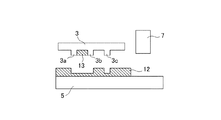
次に、モールド3の凹凸パターンに異常がある場合の一般的なインプリント装置によるパターン形成工程について説明する。例えば、図3は、欠損した凸部3a´を有するモールド3を使用した場合のパターン形成工程を示す概略図である。ここで、図3a〜図3dに示す工程は、図2a〜図2dに示す工程にそれぞれ対応している。図3に示すように、モールド3に欠損した凸部3a´が存在すると、そのパターン形状がそのまま樹脂12に転写され、インプリント装置は、欠損した微細パターン部12aを形成することになる。一方、図4は、凹凸パターンにおける凸部3aと凸部3bとの間の凹部に付着物13が存在するモールド3を使用した場合のパターン形成工程を示す概略図である。ここで、図4は、図3(d)に示す工程に対応している。通常、インプリント装置は、樹脂12が完全に硬化してから、モールド3を引き剥がすが、樹脂12が完全に硬化する前にモールド3を引き剥がしてしまう場合がある。この場合、図4に示すように、樹脂12の一部が付着物13として凹凸パターンの凹部に付着し、凹凸パターンの異常となる。
Next, a pattern forming process by a general imprint apparatus when there is an abnormality in the uneven pattern of the
インプリント装置では、モールド3に形成された凹凸パターンの形状そのものが、ウエハ5上に形成されるデバイスパターンの線幅を決定することになる。したがって、図2に示すように、凹凸パターンに異常がない場合は、デバイスパターンの線幅には異常が生じないが、図3及び図4に示すように、凹凸パターンに異常が生じると、デバイスパターンに不良が発生することとなる。例えば、図3に示すモールド3のように、凹凸パターンに欠損が生じると、欠損部分に相当するデバイスパターンは、所望の線幅を満足できず、製品として使用できないため、歩留まりの悪化となる。更に、図4に示すモールド3のように、凹凸パターンに付着物が付着したモールド3を使い続けると、付着部分に相当するデバイスパターンは、所望の線幅より太い線幅となり、この場合も、製品として使用できないため、歩留まりの悪化となる。一般に、インプリント装置では、1つのモールド3を繰り返し使用し、複数のデバイスパターンを形成するため、ダメージを受けて凹凸パターンに上記のような異常が生じる可能性は、特に考えられる。そこで、本発明では、インプリント装置1内に搭載されたモールド計測系8により、モールド3の凹凸パターン自体を計測することで、凹凸パターンの異常を簡易的に判定する。
In the imprint apparatus, the shape of the concavo-convex pattern formed on the
次に、本実施形態に係るインプリント装置1の作用について説明する。まず、インプリント装置1における凹凸パターンの状態を計測するモールド計測系8の位置関係について説明する。図5は、インプリント装置1におけるモールド計測系8の位置関係を示す概略図である。特に、図5(a)は、インプリント装置1の内部にモールド3が装填された後に、ウエハ5の交換時に、モールド3に対してモールド計測系8を走査させるパターン検査の場合の位置関係を示す概略図である。なお、この場合の「ウエハ交換時」とは、ウエハステージ6に保持された第1のウエハ(第1の基板)5を、新たな第2のウエハ(第2の基板)5に交換する時を示す。この場合、制御装置9は、ウエハ5の交換時、即ち、図5(a)に示すように、ウエハステージ6が押印位置から移動している間に、インプリントヘッド4に装填されたモールド3の凹凸パターンの計測を行うようにモールド計測系8を制御する。具体的には、モールド計測系8は、インプリント処理中には、モールド3の周辺位置に待機しており、インプリント処理が終了し、ウエハ5の交換のためにウエハステージ6が移動した後、モールド3の直下の空いた空間に移動する。この方式の利点は、モールド計測系8は、ウエハ5の交換時のウエハステージ6の移動に伴って、モールド3の凹凸パターンの計測を自動で実施するので、スループットに影響を与えることがない点にある。なお、モールド計測系8は、ウエハ5の交換時に、凹凸パターンを毎回計測できるように、ウエハステージ6の一部(例えば、側面部)に一体として配置しても良い。
Next, the operation of the
一方、図5(b)は、インプリント装置1の内部にモールド3が装填された後に、モールド3の交換時に、モールド計測系8に対してモールド3を走査させるパターン検査の場合の位置関係を示す概略図である。なお、この場合の「モールド交換時」とは、インプリント処理後に、既に保持されているモールド(第1の型)3を交換する場合と、一方、インプリント処理前に、これから保持されるモールド(第2の型)3を交換する場合とを含む。即ち、制御装置9は、図5(b)に示すように、モールド(第1の型)3をインプリントヘッド4から取り外して移動させている間に、モールド3の凹凸パターンの計測を自動で実施するようにモールド計測系8を制御する。若しくは、制御装置9は、モールド(第2の型)3をインプリントヘッド4に向けて移動させている間に、モールド3の凹凸パターンの計測を自動で実施するようにモールド計測系8を制御する。この方式の利点は、一般にインプリント装置では、形成するデバイスパターンの線幅によってモールド3を交換する必要があるため、モールド3を交換する頻度が多い場合に好適となる点にある。
On the other hand, FIG. 5B shows the positional relationship in the case of pattern inspection in which the
次に、凹凸パターンの走査計測時におけるモールド計測系8の動作について説明する。図6は、走査計測時のモールド計測系8の動作を示す概略図である。ここで、図6に示す走査計測は、図5(a)に対応し、モールド3がインプリントヘッド4に装填された状態で、モールド3に対してモールド計測系8がX軸方向で紙面左側より右側へ走査する場合を想定する。モールド計測系8は、以下の図6(a)〜図6(c)に示すような走査計測を連続して実施する。まず、図6(a)に示すように、モールド計測系8は、モールド3の凹凸パターンの最端部から中心部に向かって走査計測を行い、逐一計測信号を得て、まず、凸部3aの計測信号を得る。引き続き、モールド計測系8は、走査計測を行い、図6(b)に示すように、凹凸パターンの中心部において凸部3bの計測信号を得る。更に引き続き、モールド計測系8は、モールド3の凹凸パターンの中心部から一方の最端部に向かって走査計測を行い、図6(c)に示すように、凸部3cの計測信号を得る。
Next, the operation of the
次に、モールド計測系8が走査計測にて計測する計測信号について説明する。図7は、モールド計測系8によるモールド3の各状態における計測信号を示す概略図である。本実施形態では、まず、モールド計測系8は、インプリント装置1の外部から内部にモールド3が装填された際、装填されたモールド3の凹凸パターンを走査計測し、該走査計測で得られた信号を基準信号として、制御装置9内の記憶手段等に記憶する。図7(a)は、最初に使用するモールド3の凹凸パターンの基準信号を示す図である。図7(a)に示すように、モールド3は、まだインプリント処理に使用されておらず、凹凸パターンに異常がない新品であるので、基準信号60は、各凸部3a〜3cにおいて均一な山型形状のパターン信号部61を有する。
Next, measurement signals measured by the
次に、インプリント装置1でモールド3を使用する過程で、モールド3に欠損が生じた場合について説明する。図7(b)は、凹凸パターンに欠損した凸部3a´が存在する場合の計測信号及び指標データを示す図である。まず、モールド計測系8は、走査計測により、図7(b)に示すような計測信号62を得る。この場合、計測信号62は、凹凸パターンの凸部3a´に欠損が存在するので、凸部3a´に対応する部分には、他の信号形状とは異なる山型形状のパターン信号部63を有する。次に、制御装置9は、得られた計測信号62と、予め記憶した基準信号60とを比較することで、図7(b)に示すような指標データ64を得る。この指標データ64は、例えば、基準信号60と得られた計測信号62との差分を計算して算出された差分データである。なお、指標データ(指標)は、差分データに限定するものではなく、基準信号と得られた計測信号との相違を示すものであればよい。例えば、指標データは、信号の全体又は対応する各部分に関して求めた計測信号と基準信号との相関度(相関係数)であってもよい。次に、制御装置9は、算出した指標データ64の値が、予め設定した上限値及び下限値を有する閾値65を超えたかどうかを判定した情報である指標情報を得て、コンソール部10に出力する。ここで、制御装置9は、図7(b)に示すように、万が一閾値65を超えた場合は、モールド3に異常が発生したと判定し、コンソール部10に対して異常の発生を通知し、コンソール部10は、エラー表示を行う。これにより、ユーザーは、モールド3に異常が生じたことを即座に確認することができる。
Next, a case where a defect occurs in the
次に、インプリント装置1でモールド3を使用する過程で、モールド3に付着物が存在した場合について説明する。図7(c)は、凹凸パターンに、付着物13が存在する場合の計測信号及び指標データを示す図である。この場合も、モールド計測系8は、走査計測により、図7(c)に示すような計測信号66を得る。該計測信号66は、凹凸パターンに付着物13が存在するので、付着物13に対応する部分には、他の信号形状とは異なる大きな山型形状のパターン信号部67を有する。次に、制御装置9は、得られた計測信号66と、予め記憶した基準信号60とを比較することで、図7(c)に示すような指標データ68を得る。次に、制御装置9は、算出した指標データ68の値が、予め設定した閾値65を超えたかどうかを判定した情報である指標情報を得て、コンソール部10に出力する。この場合も、制御装置9は、図7(c)に示すように、万が一閾値65を超えた場合は、モールド3に異常が発生したと判定する。コンソール部10によるエラー表示は、上記と同様である。
Next, a case where deposits are present in the
なお、比較のために、インプリント装置1でモールド3を使用する過程で、モールド3には異常が生じなかった場合について説明する。図7(d)は、凹凸パターンに異常がない場合の計測信号及び指標データを示す図である。この場合も、モールド計測系8は、走査計測により、図7(d)に示すような計測信号70を得るが、凹凸パターンには異常がないので、計測信号70は、基準信号60と同等の信号となる。次に、制御装置9は、得られた計測信号70と、予め記憶した基準信号60とを比較することで、図7(c)に示すような指標データ72を得る。そして、制御装置9は、算出した指標データ72の値が予め設定した閾値65を超えたかどうかを判定した情報である指標情報を得て、コンソール部10に出力する。この場合は、制御装置9は、図7(d)に示すように、指標データ72は閾値65を超えないので、モールド3には異常がないと判定する。
For comparison, a case where no abnormality occurs in the
以上のように、本実施形態のインプリント装置1によれば、インプリント装置1内に設置されたモールド計測系8により、簡易にモールド3の凹凸パターンを検査することができるので、モールド3に異常が生じた際は、即座にモールド3を交換することができる。したがって、インプリント装置1により製造される物品の歩留まりに対して有利である。
As described above, according to the
(物品の製造方法)
物品としてのデバイス(半導体集積回路素子、液晶表示素子等)の製造方法は、上述したインプリント装置を用いて基板(ウエハ、ガラスプレート、フィルム状基板)にパターンを形成する工程を含む。更に、該製造方法は、パターンが形成された基板をエッチングする工程を含みうる。なお、パターンドメディア(記録媒体)や光学素子等の他の物品を製造する場合には、該製造方法は、エッチングの代わりに、パターンが形成された基板を加工する他の処理を含みうる。本実施形態の物品の製造方法は、従来の方法に比べて、物品の性能・品質・生産性・生産コストの少なくとも1つにおいて有利である。
(Product manufacturing method)
A method for manufacturing a device (semiconductor integrated circuit element, liquid crystal display element, etc.) as an article includes a step of forming a pattern on a substrate (wafer, glass plate, film-like substrate) using the above-described imprint apparatus. Furthermore, the manufacturing method may include a step of etching the substrate on which the pattern is formed. In the case of manufacturing other articles such as patterned media (recording media) and optical elements, the manufacturing method may include other processes for processing a substrate on which a pattern is formed instead of etching. The method for manufacturing an article according to the present embodiment is advantageous in at least one of the performance, quality, productivity, and production cost of the article as compared with the conventional method.
以上、本発明の好ましい実施形態について説明したが、本発明はこれらの実施形態に限定されず、その要旨の範囲内で種々の変形及び変更が可能である。 As mentioned above, although preferable embodiment of this invention was described, this invention is not limited to these embodiment, A various deformation | transformation and change are possible within the range of the summary.
例えば、図7では、信号について、簡単化のために1次元的に説明したが、実際のモールド3は2次元であり、モールド計測系8は、モールド3を2次元で計測するとより好適である。また、図7に示した、制御装置9に予め設定した、ある一定の閾値65は、常に一定ではなく、任意のタイミングで書き換えても良い。
For example, in FIG. 7, the signal is described one-dimensionally for simplification. However, the
1 インプリント装置
3 モールド
5 ウエハ
8 モールド計測系
8a 投光部
8b 受光部
9 制御装置
10 コンソール部
12 紫外線硬化樹脂
DESCRIPTION OF
Claims (14)
前記型に投光して該型で生じた散乱光を受光して計測信号を得る計測手段と、
制御手段と、を有し、
前記制御手段は、基準信号、上限値および下限値を記憶し、前記型に関して前記計測手段に前記計測信号を得させ、該計測信号と前記基準信号との相違を示す指標を求め、前記上限値および前記下限値のいずれを前記指標が超えたかを示す情報を出力し、
前記上限値は、前記型の欠損および前記型への異物の付着のうちの一方に対応する閾値であり、前記下限値は、前記欠損および前記付着のうちの他方に対応する閾値である、
ことを特徴とするインプリント装置。 An imprint apparatus for forming an uncured resin on a substrate with a mold to form a resin pattern on the substrate,
Measuring means for projecting light onto the mold and receiving scattered light generated by the mold to obtain a measurement signal;
Control means, and
The control means stores a reference signal, an upper limit value and a lower limit value, causes the measurement means to obtain the measurement signal with respect to the mold, obtains an index indicating a difference between the measurement signal and the reference signal, and determines the upper limit value. And information indicating which of the lower limits the indicator has exceeded ,
The upper limit value is a threshold value corresponding to one of the defect of the mold and the adhesion of foreign matter to the mold, and the lower limit value is a threshold value corresponding to the other of the defect and the adhesion,
An imprint apparatus characterized by that.
前記制御手段は、前記情報を前記コンソール部に出力させる、ことを特徴とする請求項1ないし請求項3のいずれか1項に記載のインプリント装置。 Having a console part,
The imprint apparatus according to claim 1, wherein the control unit causes the console unit to output the information.
前記制御手段は、前記型保持手段に保持された第1の型を第2の型と交換する場合に、前記第1の型に関して前記計測手段に前記計測信号を得させる、ことを特徴とする請求項1ないし請求項4のいずれか1項に記載のインプリント装置。 Having mold holding means for holding the mold;
The control means causes the measurement means to obtain the measurement signal with respect to the first mold when the first mold held by the mold holding means is replaced with a second mold. The imprint apparatus according to any one of claims 1 to 4.
前記制御手段は、前記型保持手段に保持された第1の型を第2の型と交換する場合に、前記第2の型に関して前記計測手段に前記計測信号を得させる、ことを特徴とする請求項1ないし請求項4のいずれか1項に記載のインプリント装置。 Having mold holding means for holding the mold;
The control means causes the measurement means to obtain the measurement signal for the second mold when the first mold held by the mold holding means is replaced with a second mold. The imprint apparatus according to any one of claims 1 to 4.
前記制御手段は、前記基板保持手段に保持された第1の基板を第2の基板に交換する間に、前記型に関して前記計測手段に前記計測信号を得させる、ことを特徴とする請求項1ないし請求項4のいずれか1項に記載のインプリント装置。 Having substrate holding means for holding the substrate;
2. The control unit causes the measurement unit to obtain the measurement signal for the mold while exchanging the first substrate held by the substrate holding unit with a second substrate. The imprint apparatus according to claim 4.
前記計測手段は、前記投光を行う投光部と、前記受光を行う受光部とを有し、
前記投光部と前記受光部とは、前記基板保持手段に配置され、
前記制御手段は、前記型保持手段に保持された前記型に対して前記基板保持手段を移動させて前記型に関して前記計測手段に前記計測信号を得させる、ことを特徴とする請求項1ないし請求項4のいずれか1項に記載のインプリント装置。 A mold holding means for holding the mold, and a movable substrate holding means for holding the substrate;
The measuring means includes a light projecting unit that performs the light projection and a light receiving unit that performs the light reception,
The light projecting unit and the light receiving unit are disposed on the substrate holding unit,
2. The control unit according to claim 1, wherein the control unit moves the substrate holding unit with respect to the mold held by the mold holding unit to cause the measurement unit to obtain the measurement signal with respect to the mold. Item 5. The imprint apparatus according to any one of items 4.
前記型に投光して該型で生じた散乱光を受光して計測信号を得る計測手段と、
制御手段と、を有し、
前記制御手段は、前記型に対応する基準信号を記憶し、前記型に関して前記計測手段に前記計測信号を得させ、該計測信号と前記基準信号との相違を示す指標を求め、該指標に対する閾値としての上限値および下限値のいずれを該指標が超えたかを示す情報を出力し、
前記上限値は、前記型の欠損および前記型への異物の付着のうちの一方に対応する閾値であり、前記下限値は、前記欠損および前記付着のうちの他方に対応する閾値である、
ことを特徴とするインプリント装置。 An imprint apparatus for forming an uncured resin on a substrate with a mold to form a resin pattern on the substrate,
Measuring means for projecting light onto the mold and receiving scattered light generated by the mold to obtain a measurement signal;
Control means, and
The control means stores a reference signal corresponding to the mold, causes the measurement means to obtain the measurement signal with respect to the mold, obtains an index indicating a difference between the measurement signal and the reference signal, and a threshold for the index any upper limit value and the lower limit value and outputs the information indicating whether the index is above as,
The upper limit value is a threshold value corresponding to one of the defect of the mold and the adhesion of foreign matter to the mold, and the lower limit value is a threshold value corresponding to the other of the defect and the adhesion,
An imprint apparatus characterized by that.
前記工程で前記パターンを形成された基板を加工する工程と、
を含む、ことを特徴とする物品の製造方法。 Forming a resin pattern on a substrate using the imprint apparatus according to any one of claims 1 to 11 ,
Processing the substrate on which the pattern is formed in the step;
A method for producing an article comprising:
前記型に投光して該型で生じた散乱光を受光して計測信号を得る計測手段と、
制御手段と、を有し、
前記制御手段は、基準信号、上限値および下限値を記憶し、前記型に関して前記計測手段に前記計測信号を得させ、該計測信号と前記基準信号との相違を示す指標を求め、前記上限値および前記下限値のいずれを前記指標が超えたかを示す情報を出力し、
前記上限値は、前記型の欠損および前記型への異物の付着のうちの一方に対応する閾値であり、前記下限値は、前記欠損および前記付着のうちの他方に対応する閾値である、
ことを特徴とする検査装置。 An inspection device for inspecting a mold,
Measuring means for projecting light onto the mold and receiving scattered light generated by the mold to obtain a measurement signal;
Control means, and
The control means stores a reference signal, an upper limit value and a lower limit value, causes the measurement means to obtain the measurement signal with respect to the mold, obtains an index indicating a difference between the measurement signal and the reference signal, and determines the upper limit value. And information indicating which of the lower limits the indicator has exceeded ,
The upper limit value is a threshold value corresponding to one of the defect of the mold and the adhesion of foreign matter to the mold, and the lower limit value is a threshold value corresponding to the other of the defect and the adhesion,
Inspection apparatus characterized by that.
前記型に投光して該型で生じた散乱光を受光して計測信号を得る計測手段と、
制御手段と、を有し、
前記制御手段は、前記型に対応する基準信号を記憶し、前記型に関して前記計測手段に前記計測信号を得させ、該計測信号と前記基準信号との相違を示す指標を求め、該指標に対する閾値としての上限値および下限値のいずれを該指標が超えたかを示す情報を出力し、
前記上限値は、前記型の欠損および前記型への異物の付着のうちの一方に対応する閾値であり、前記下限値は、前記欠損および前記付着のうちの他方に対応する閾値である、
ことを特徴とする検査装置。 An inspection apparatus for inspecting the mold with respect to the defect of the mold and adhesion of foreign matter to the mold,
Measuring means for projecting light onto the mold and receiving scattered light generated by the mold to obtain a measurement signal;
Control means, and
The control means stores a reference signal corresponding to the mold, causes the measurement means to obtain the measurement signal with respect to the mold, obtains an index indicating a difference between the measurement signal and the reference signal, and a threshold for the index any upper limit value and the lower limit value and outputs the information indicating whether the index is above as,
The upper limit value is a threshold value corresponding to one of the defect of the mold and the adhesion of foreign matter to the mold, and the lower limit value is a threshold value corresponding to the other of the defect and the adhesion,
Inspection apparatus characterized by that.
Priority Applications (2)
| Application Number | Priority Date | Filing Date | Title |
|---|---|---|---|
| JP2010032037A JP5697345B2 (en) | 2010-02-17 | 2010-02-17 | Imprint apparatus and article manufacturing method |
| US13/025,436 US9535321B2 (en) | 2010-02-17 | 2011-02-11 | Imprint apparatus and article manufacturing method |
Applications Claiming Priority (1)
| Application Number | Priority Date | Filing Date | Title |
|---|---|---|---|
| JP2010032037A JP5697345B2 (en) | 2010-02-17 | 2010-02-17 | Imprint apparatus and article manufacturing method |
Publications (3)
| Publication Number | Publication Date |
|---|---|
| JP2011171410A JP2011171410A (en) | 2011-09-01 |
| JP2011171410A5 JP2011171410A5 (en) | 2013-04-04 |
| JP5697345B2 true JP5697345B2 (en) | 2015-04-08 |
Family
ID=44369083
Family Applications (1)
| Application Number | Title | Priority Date | Filing Date |
|---|---|---|---|
| JP2010032037A Active JP5697345B2 (en) | 2010-02-17 | 2010-02-17 | Imprint apparatus and article manufacturing method |
Country Status (2)
| Country | Link |
|---|---|
| US (1) | US9535321B2 (en) |
| JP (1) | JP5697345B2 (en) |
Families Citing this family (11)
| Publication number | Priority date | Publication date | Assignee | Title |
|---|---|---|---|---|
| JP2013098181A (en) * | 2011-10-27 | 2013-05-20 | Canon Inc | Imprint device, imprint method, imprint system, and device manufacturing method |
| JP6188382B2 (en) * | 2013-04-03 | 2017-08-30 | キヤノン株式会社 | Imprint apparatus and article manufacturing method |
| JP6333039B2 (en) | 2013-05-16 | 2018-05-30 | キヤノン株式会社 | Imprint apparatus, device manufacturing method, and imprint method |
| JP6315904B2 (en) * | 2013-06-28 | 2018-04-25 | キヤノン株式会社 | Imprint method, imprint apparatus, and device manufacturing method |
| KR102215539B1 (en) * | 2015-11-20 | 2021-02-16 | 에이에스엠엘 네델란즈 비.브이. | Lithographic apparatus and method of operating lithographic apparatus |
| JP6671160B2 (en) | 2015-11-30 | 2020-03-25 | キヤノン株式会社 | Imprint apparatus, article manufacturing method and alignment method |
| JP6821414B2 (en) * | 2016-12-13 | 2021-01-27 | キヤノン株式会社 | Imprinting equipment and manufacturing method of articles |
| JP7262939B2 (en) * | 2018-07-20 | 2023-04-24 | キヤノン株式会社 | Cleaning apparatus, imprint apparatus, lithographic apparatus, and cleaning method |
| JP7129259B2 (en) * | 2018-07-24 | 2022-09-01 | キヤノン株式会社 | Inspection method, imprint apparatus, and article manufacturing method |
| JP7117955B2 (en) * | 2018-09-18 | 2022-08-15 | キヤノン株式会社 | IMPRINT METHOD, IMPRINT APPARATUS, AND ARTICLE MANUFACTURING METHOD |
| JP2022034165A (en) * | 2020-08-18 | 2022-03-03 | Towa株式会社 | Inspection device, resin molding device, and manufacturing method of resin molded article |
Family Cites Families (13)
| Publication number | Priority date | Publication date | Assignee | Title |
|---|---|---|---|---|
| JPH04355350A (en) * | 1991-05-31 | 1992-12-09 | Dainippon Printing Co Ltd | Defect inspector |
| JP2647051B2 (en) * | 1995-03-09 | 1997-08-27 | 日本電気株式会社 | Appearance inspection device |
| US20050037143A1 (en) * | 2000-07-18 | 2005-02-17 | Chou Stephen Y. | Imprint lithography with improved monitoring and control and apparatus therefor |
| JP2005191444A (en) * | 2003-12-26 | 2005-07-14 | Bussan Nanotech Research Institute Inc | Pattern transferring equipment, mold cleaning method, and pattern transferring method |
| US7019835B2 (en) | 2004-02-19 | 2006-03-28 | Molecular Imprints, Inc. | Method and system to measure characteristics of a film disposed on a substrate |
| JP2005214980A (en) * | 2005-01-31 | 2005-08-11 | Miyazaki Oki Electric Co Ltd | Macro inspection method for wafer and automatic wafer macro inspection device |
| JP2006228843A (en) * | 2005-02-16 | 2006-08-31 | Renesas Technology Corp | Process control method and manufacturing method of semiconductor device |
| JP4594833B2 (en) * | 2005-09-09 | 2010-12-08 | 株式会社堀場製作所 | Defect inspection equipment |
| JP2008194838A (en) * | 2007-02-08 | 2008-08-28 | Sii Nanotechnology Inc | Method for testing nano-imprint lithography mold and method for removing resin residue |
| JP2008276920A (en) * | 2007-03-30 | 2008-11-13 | Pioneer Electronic Corp | Imprint device and imprint method |
| JP2008302519A (en) * | 2007-06-05 | 2008-12-18 | Hitachi Maxell Ltd | Nanoimprint apparatus and nanoimprint method |
| JP2009143089A (en) * | 2007-12-13 | 2009-07-02 | Hitachi Industrial Equipment Systems Co Ltd | Mold for fine-structure transfer and its manufacturing method |
| WO2009153926A1 (en) * | 2008-06-18 | 2009-12-23 | 株式会社ニコン | Template manufacturing method, template inspecting method and inspecting apparatus, nanoimprint apparatus, nanoimprint system, and device manufacturing method |
-
2010
- 2010-02-17 JP JP2010032037A patent/JP5697345B2/en active Active
-
2011
- 2011-02-11 US US13/025,436 patent/US9535321B2/en active Active
Also Published As
| Publication number | Publication date |
|---|---|
| JP2011171410A (en) | 2011-09-01 |
| US9535321B2 (en) | 2017-01-03 |
| US20110198769A1 (en) | 2011-08-18 |
Similar Documents
| Publication | Publication Date | Title |
|---|---|---|
| JP5697345B2 (en) | Imprint apparatus and article manufacturing method | |
| JP5173944B2 (en) | Imprint apparatus and article manufacturing method | |
| US20220026800A1 (en) | Imprint apparatus, imprinting method, and method of manufacturing product | |
| JP4963718B2 (en) | Imprint method, imprint apparatus, and article manufacturing method using the same | |
| US9387607B2 (en) | Imprint apparatus, imprint method, and method for producing device | |
| CN106918986B (en) | Adjusting method of imprint apparatus, imprint method, and article manufacturing method | |
| JP6029268B2 (en) | Imprint apparatus and article manufacturing method using the same | |
| JP6457773B2 (en) | Imprint method, imprint apparatus and article manufacturing method | |
| JP2012178470A (en) | Imprint device and device manufacturing method | |
| JP6363838B2 (en) | Imprint apparatus, imprint method, and article manufacturing method | |
| JP2016027623A (en) | Method of creating supplying pattern of imprint material, imprint method and device, and article manufacturing method | |
| JP2012134466A (en) | Imprint apparatus, manufacturing method of article using the same | |
| KR20170063366A (en) | Imprint apparatus and method for producing article | |
| JP5936373B2 (en) | Imprint apparatus, imprint apparatus control method, and device manufacturing method | |
| US20150151462A1 (en) | Imprint method | |
| US8770964B2 (en) | Imprint apparatus and article manufacturing method | |
| JP5448714B2 (en) | Imprint apparatus and article manufacturing method using the same | |
| JP7278828B2 (en) | Molding method, molding apparatus, imprinting method, and article manufacturing method | |
| JP6450105B2 (en) | Imprint apparatus and article manufacturing method | |
| JP6643022B2 (en) | Imprint apparatus, imprint method, foreign matter detection method, and article manufacturing method | |
| JP6541518B2 (en) | Imprint apparatus, imprint method, and article manufacturing method | |
| TWI486579B (en) | Detection apparatus, lithography apparatus, method of manufacturing article, and detection method | |
| US20210379800A1 (en) | Imprint device, article manufacturing method, and measuring method for imprint device | |
| JP2023020870A (en) | Information processing device, molding device, molding method and method for manufacturing article | |
| TWI429531B (en) | Imprint apparatus, and article manufacturing method using same |
Legal Events
| Date | Code | Title | Description |
|---|---|---|---|
| A521 | Written amendment |
Free format text: JAPANESE INTERMEDIATE CODE: A523 Effective date: 20130218 |
|
| A621 | Written request for application examination |
Free format text: JAPANESE INTERMEDIATE CODE: A621 Effective date: 20130218 |
|
| A977 | Report on retrieval |
Free format text: JAPANESE INTERMEDIATE CODE: A971007 Effective date: 20131030 |
|
| A131 | Notification of reasons for refusal |
Free format text: JAPANESE INTERMEDIATE CODE: A131 Effective date: 20131119 |
|
| A521 | Written amendment |
Free format text: JAPANESE INTERMEDIATE CODE: A523 Effective date: 20140117 |
|
| A131 | Notification of reasons for refusal |
Free format text: JAPANESE INTERMEDIATE CODE: A131 Effective date: 20140603 |
|
| A521 | Written amendment |
Free format text: JAPANESE INTERMEDIATE CODE: A523 Effective date: 20140804 |
|
| TRDD | Decision of grant or rejection written | ||
| A01 | Written decision to grant a patent or to grant a registration (utility model) |
Free format text: JAPANESE INTERMEDIATE CODE: A01 Effective date: 20150113 |
|
| A61 | First payment of annual fees (during grant procedure) |
Free format text: JAPANESE INTERMEDIATE CODE: A61 Effective date: 20150210 |
|
| R151 | Written notification of patent or utility model registration |
Ref document number: 5697345 Country of ref document: JP Free format text: JAPANESE INTERMEDIATE CODE: R151 |