JP5657352B2 - Exposure amount evaluation method and reflection type substrate - Google Patents
Exposure amount evaluation method and reflection type substrate Download PDFInfo
- Publication number
- JP5657352B2 JP5657352B2 JP2010252134A JP2010252134A JP5657352B2 JP 5657352 B2 JP5657352 B2 JP 5657352B2 JP 2010252134 A JP2010252134 A JP 2010252134A JP 2010252134 A JP2010252134 A JP 2010252134A JP 5657352 B2 JP5657352 B2 JP 5657352B2
- Authority
- JP
- Japan
- Prior art keywords
- light
- euv
- exposure
- substrate
- long
- Prior art date
- Legal status (The legal status is an assumption and is not a legal conclusion. Google has not performed a legal analysis and makes no representation as to the accuracy of the status listed.)
- Expired - Fee Related
Links
- 239000000758 substrate Substances 0.000 title claims description 41
- 238000011156 evaluation Methods 0.000 title claims description 16
- 238000010521 absorption reaction Methods 0.000 claims description 40
- 238000009826 distribution Methods 0.000 claims description 19
- 238000012546 transfer Methods 0.000 claims description 15
- 238000002310 reflectometry Methods 0.000 claims description 9
- 230000001678 irradiating effect Effects 0.000 claims description 5
- 230000003287 optical effect Effects 0.000 claims description 5
- 238000005259 measurement Methods 0.000 claims description 4
- 239000010410 layer Substances 0.000 description 94
- 238000010586 diagram Methods 0.000 description 16
- 229910016006 MoSi Inorganic materials 0.000 description 13
- 239000000463 material Substances 0.000 description 6
- 238000004088 simulation Methods 0.000 description 6
- 239000002131 composite material Substances 0.000 description 5
- 239000004065 semiconductor Substances 0.000 description 5
- 238000004519 manufacturing process Methods 0.000 description 4
- 238000000034 method Methods 0.000 description 4
- 238000012545 processing Methods 0.000 description 4
- 238000004364 calculation method Methods 0.000 description 3
- 238000011161 development Methods 0.000 description 2
- 238000010894 electron beam technology Methods 0.000 description 2
- 239000011521 glass Substances 0.000 description 2
- 230000031700 light absorption Effects 0.000 description 2
- 238000001579 optical reflectometry Methods 0.000 description 2
- 238000002834 transmittance Methods 0.000 description 2
- VYZAMTAEIAYCRO-UHFFFAOYSA-N Chromium Chemical compound [Cr] VYZAMTAEIAYCRO-UHFFFAOYSA-N 0.000 description 1
- 230000002238 attenuated effect Effects 0.000 description 1
- YXTPWUNVHCYOSP-UHFFFAOYSA-N bis($l^{2}-silanylidene)molybdenum Chemical compound [Si]=[Mo]=[Si] YXTPWUNVHCYOSP-UHFFFAOYSA-N 0.000 description 1
- 238000012937 correction Methods 0.000 description 1
- 238000005520 cutting process Methods 0.000 description 1
- 230000007423 decrease Effects 0.000 description 1
- 238000013461 design Methods 0.000 description 1
- 239000006185 dispersion Substances 0.000 description 1
- 238000005530 etching Methods 0.000 description 1
- 238000007689 inspection Methods 0.000 description 1
- 238000012986 modification Methods 0.000 description 1
- 230000004048 modification Effects 0.000 description 1
- 229910021344 molybdenum silicide Inorganic materials 0.000 description 1
- 238000000059 patterning Methods 0.000 description 1
- 230000000737 periodic effect Effects 0.000 description 1
- 230000002093 peripheral effect Effects 0.000 description 1
- 239000002356 single layer Substances 0.000 description 1
- 229910052715 tantalum Inorganic materials 0.000 description 1
- GUVRBAGPIYLISA-UHFFFAOYSA-N tantalum atom Chemical compound [Ta] GUVRBAGPIYLISA-UHFFFAOYSA-N 0.000 description 1
- 238000012360 testing method Methods 0.000 description 1
Images


Classifications
-
- G—PHYSICS
- G03—PHOTOGRAPHY; CINEMATOGRAPHY; ANALOGOUS TECHNIQUES USING WAVES OTHER THAN OPTICAL WAVES; ELECTROGRAPHY; HOLOGRAPHY
- G03F—PHOTOMECHANICAL PRODUCTION OF TEXTURED OR PATTERNED SURFACES, e.g. FOR PRINTING, FOR PROCESSING OF SEMICONDUCTOR DEVICES; MATERIALS THEREFOR; ORIGINALS THEREFOR; APPARATUS SPECIALLY ADAPTED THEREFOR
- G03F1/00—Originals for photomechanical production of textured or patterned surfaces, e.g., masks, photo-masks, reticles; Mask blanks or pellicles therefor; Containers specially adapted therefor; Preparation thereof
- G03F1/22—Masks or mask blanks for imaging by radiation of 100nm or shorter wavelength, e.g. X-ray masks, extreme ultraviolet [EUV] masks; Preparation thereof
- G03F1/24—Reflection masks; Preparation thereof
-
- G—PHYSICS
- G01—MEASURING; TESTING
- G01J—MEASUREMENT OF INTENSITY, VELOCITY, SPECTRAL CONTENT, POLARISATION, PHASE OR PULSE CHARACTERISTICS OF INFRARED, VISIBLE OR ULTRAVIOLET LIGHT; COLORIMETRY; RADIATION PYROMETRY
- G01J1/00—Photometry, e.g. photographic exposure meter
- G01J1/42—Photometry, e.g. photographic exposure meter using electric radiation detectors
- G01J1/429—Photometry, e.g. photographic exposure meter using electric radiation detectors applied to measurement of ultraviolet light
-
- G—PHYSICS
- G03—PHOTOGRAPHY; CINEMATOGRAPHY; ANALOGOUS TECHNIQUES USING WAVES OTHER THAN OPTICAL WAVES; ELECTROGRAPHY; HOLOGRAPHY
- G03F—PHOTOMECHANICAL PRODUCTION OF TEXTURED OR PATTERNED SURFACES, e.g. FOR PRINTING, FOR PROCESSING OF SEMICONDUCTOR DEVICES; MATERIALS THEREFOR; ORIGINALS THEREFOR; APPARATUS SPECIALLY ADAPTED THEREFOR
- G03F1/00—Originals for photomechanical production of textured or patterned surfaces, e.g., masks, photo-masks, reticles; Mask blanks or pellicles therefor; Containers specially adapted therefor; Preparation thereof
- G03F1/68—Preparation processes not covered by groups G03F1/20 - G03F1/50
- G03F1/82—Auxiliary processes, e.g. cleaning or inspecting
- G03F1/84—Inspecting
-
- G—PHYSICS
- G03—PHOTOGRAPHY; CINEMATOGRAPHY; ANALOGOUS TECHNIQUES USING WAVES OTHER THAN OPTICAL WAVES; ELECTROGRAPHY; HOLOGRAPHY
- G03F—PHOTOMECHANICAL PRODUCTION OF TEXTURED OR PATTERNED SURFACES, e.g. FOR PRINTING, FOR PROCESSING OF SEMICONDUCTOR DEVICES; MATERIALS THEREFOR; ORIGINALS THEREFOR; APPARATUS SPECIALLY ADAPTED THEREFOR
- G03F7/00—Photomechanical, e.g. photolithographic, production of textured or patterned surfaces, e.g. printing surfaces; Materials therefor, e.g. comprising photoresists; Apparatus specially adapted therefor
- G03F7/70—Microphotolithographic exposure; Apparatus therefor
- G03F7/70483—Information management; Active and passive control; Testing; Wafer monitoring, e.g. pattern monitoring
- G03F7/70605—Workpiece metrology
- G03F7/70616—Monitoring the printed patterns
- G03F7/70625—Dimensions, e.g. line width, critical dimension [CD], profile, sidewall angle or edge roughness
-
- G—PHYSICS
- G03—PHOTOGRAPHY; CINEMATOGRAPHY; ANALOGOUS TECHNIQUES USING WAVES OTHER THAN OPTICAL WAVES; ELECTROGRAPHY; HOLOGRAPHY
- G03F—PHOTOMECHANICAL PRODUCTION OF TEXTURED OR PATTERNED SURFACES, e.g. FOR PRINTING, FOR PROCESSING OF SEMICONDUCTOR DEVICES; MATERIALS THEREFOR; ORIGINALS THEREFOR; APPARATUS SPECIALLY ADAPTED THEREFOR
- G03F7/00—Photomechanical, e.g. photolithographic, production of textured or patterned surfaces, e.g. printing surfaces; Materials therefor, e.g. comprising photoresists; Apparatus specially adapted therefor
- G03F7/70—Microphotolithographic exposure; Apparatus therefor
- G03F7/708—Construction of apparatus, e.g. environment aspects, hygiene aspects or materials
- G03F7/7085—Detection arrangement, e.g. detectors of apparatus alignment possibly mounted on wafers, exposure dose, photo-cleaning flux, stray light, thermal load
-
- G—PHYSICS
- G03—PHOTOGRAPHY; CINEMATOGRAPHY; ANALOGOUS TECHNIQUES USING WAVES OTHER THAN OPTICAL WAVES; ELECTROGRAPHY; HOLOGRAPHY
- G03F—PHOTOMECHANICAL PRODUCTION OF TEXTURED OR PATTERNED SURFACES, e.g. FOR PRINTING, FOR PROCESSING OF SEMICONDUCTOR DEVICES; MATERIALS THEREFOR; ORIGINALS THEREFOR; APPARATUS SPECIALLY ADAPTED THEREFOR
- G03F7/00—Photomechanical, e.g. photolithographic, production of textured or patterned surfaces, e.g. printing surfaces; Materials therefor, e.g. comprising photoresists; Apparatus specially adapted therefor
- G03F7/70—Microphotolithographic exposure; Apparatus therefor
- G03F7/708—Construction of apparatus, e.g. environment aspects, hygiene aspects or materials
- G03F7/70908—Hygiene, e.g. preventing apparatus pollution, mitigating effect of pollution or removing pollutants from apparatus
- G03F7/70941—Stray fields and charges, e.g. stray light, scattered light, flare, transmission loss
Landscapes
- General Physics & Mathematics (AREA)
- Physics & Mathematics (AREA)
- Epidemiology (AREA)
- Health & Medical Sciences (AREA)
- Public Health (AREA)
- Engineering & Computer Science (AREA)
- Environmental & Geological Engineering (AREA)
- Life Sciences & Earth Sciences (AREA)
- Atmospheric Sciences (AREA)
- Spectroscopy & Molecular Physics (AREA)
- Preparing Plates And Mask In Photomechanical Process (AREA)
- Exposure Of Semiconductors, Excluding Electron Or Ion Beam Exposure (AREA)
- Exposure And Positioning Against Photoresist Photosensitive Materials (AREA)
- Photometry And Measurement Of Optical Pulse Characteristics (AREA)
Description
本発明の実施形態は、露光量評価方法およびフォトマスクに関する。 Embodiments described herein relate generally to an exposure amount evaluation method and a photomask.
半導体集積回路の微細化に伴って、例えば、回路線幅が40nm未満の微細回路製造では、ArF露光装置よりも波長の短いEUV(Extreme Ultra-Violet)露光装置による製造が検討されてきており、13.5nmを中心波長とするEUV光源の開発が進められてきている。このようなEUV露光装置では、屈折光学系を構成する適切なレンズ材料(高透過率、屈折率差)が存在せず、また空気中の透過率も悪いので、真空反射光学系と反射型マスクとを用いる必要がある。 With the miniaturization of semiconductor integrated circuits, for example, in the manufacture of microcircuits having a circuit line width of less than 40 nm, manufacturing using an EUV (Extreme Ultra-Violet) exposure apparatus having a wavelength shorter than that of an ArF exposure apparatus has been studied. Development of an EUV light source having a central wavelength of 13.5 nm has been underway. In such an EUV exposure apparatus, there is no appropriate lens material (high transmittance, refractive index difference) that constitutes the refractive optical system, and the transmittance in the air is poor. Must be used.
また、EUV光領域に対し、単層で高反射率を有する材料も存在しない。このため、EUV露光で用いる全ての反射ミラー/マスクは、Bragg反射条件に整合した2種類以上の異なる材料(例えば、Mo/Si等)からなる多層膜を表面に形成することで、反射率を向上させている。 Further, there is no material having a single layer and high reflectivity with respect to the EUV light region. For this reason, all the reflective mirrors / masks used in EUV exposure are formed with a multilayer film made of two or more different materials (for example, Mo / Si, etc.) matched with the Bragg reflection conditions on the surface, thereby improving the reflectance. It is improving.
ところが、EUV露光では、各反射ミラーの反射率が1枚当たり70%ぐらいが上限である。このため、EUV光学系で必要な反射ミラーの枚数(例えば15枚程度)を考慮すると、初期EUV光量に対してウエハに照射される光量は、(0.7)^15=0.47%となる。したがって、光源出力をいかに上げるか、光の伝播効率をいかに上げるかが大きな技術課題となっている。 However, in EUV exposure, the upper limit of the reflectance of each reflecting mirror is about 70%. For this reason, in consideration of the number of reflection mirrors necessary for the EUV optical system (for example, about 15), the amount of light irradiated on the wafer with respect to the initial EUV light amount is (0.7) ^ 15 = 0.47%. Become. Therefore, how to increase the light source output and how to increase the light propagation efficiency are major technical issues.
EUV光源には、放電プラズマ型またはレーザプラズマ型があり、プラズマ種としてはXe、Snなどが用いられている。プラズマからは、EUV光の他にも種々の波長の光(Outband成分)が発生する。そして、反射光学系では色分散が存在しないので、各波長に対応する反射率で減衰した光量がマスクやウエハまで到達する。EUVレジストは、DUV(Deep Ultra Violet)領域(100nm〜200nm台)に対する感光特性を有しているので、DUV光がパターン転写特性に影響を与えることが懸念される。 EUV light sources include a discharge plasma type and a laser plasma type, and Xe, Sn, etc. are used as plasma types. From the plasma, light of various wavelengths (Outband component) is generated in addition to EUV light. Since there is no chromatic dispersion in the reflective optical system, the amount of light attenuated by the reflectance corresponding to each wavelength reaches the mask or wafer. Since the EUV resist has a photosensitive characteristic for a DUV (Deep Ultra Violet) region (on the order of 100 nm to 200 nm), there is a concern that the DUV light affects the pattern transfer characteristic.
DUV光などのOutbandが露光領域内でどのような分布をしているかを高精度に評価する方法の1つとして、ウエハステージ上やマスクステージ上などにDUV光を計測する光量モニターを設置する方法がある。しかしながら、この方法では、装置構成が複雑になるとともに、DUV光の計測に手間を要する。このため、DUV光などのOutbandを容易に評価することが望まれる。 A method of installing a light amount monitor for measuring DUV light on a wafer stage, a mask stage, etc., as one method for highly accurately evaluating how the outband such as DUV light is distributed in the exposure region There is. However, this method complicates the apparatus configuration and requires time for measuring DUV light. For this reason, it is desirable to easily evaluate outbands such as DUV light.
本発明の一つの実施形態は、EUV光以外の波長を有した露光光を容易に評価する露光量評価方法およびフォトマスクを提供する。 One embodiment of the present invention provides an exposure dose evaluation method and a photomask for easily evaluating exposure light having a wavelength other than EUV light.
本発明の一つの実施形態によれば、露光量評価方法が、セットステップと、照射ステップと、光量測定ステップと、を含んでいる。セットステップでは、フォトマスクと、レジストが塗布された露光対象の基板と、をEUV露光装置内にセットする。フォトマスクは、露光光のうちEUV光よりも長い波長を有した長波長光を反射し且つ前記EUV光を吸収する長波長光反射膜と、前記長波長光反射膜の上層側に配置されるとともに前記EUV光および前記長波長光を吸収する吸収膜を用いて形成されたマスクパターンとを有している。照射ステップでは、前記フォトマスクに対し前記マスクパターン側から前記露光光を照射するとともに、前記フォトマスクで反射された露光光を前記基板に照射する。光量測定ステップでは、前記基板に照射された露光光の露光量に基づいて、前記基板に照射された長波長光の光量分布を測定する。 According to one embodiment of the present invention, the exposure amount evaluation method includes a set step, an irradiation step, and a light amount measurement step. In the setting step, a photomask and an exposure target substrate coated with a resist are set in an EUV exposure apparatus. The photomask is disposed on the upper layer side of the long-wavelength light reflecting film, which reflects long-wavelength light having a wavelength longer than EUV light in the exposure light and absorbs the EUV light. And a mask pattern formed using an absorption film that absorbs the EUV light and the long wavelength light. In the irradiation step, the photomask is irradiated with the exposure light from the mask pattern side, and the substrate is irradiated with the exposure light reflected by the photomask. In the light amount measurement step, the light amount distribution of the long wavelength light irradiated on the substrate is measured based on the exposure amount of the exposure light irradiated on the substrate.
以下に添付図面を参照して、実施形態に係る露光量評価方法およびフォトマスクを詳細に説明する。なお、これらの実施形態により本発明が限定されるものではない。 Hereinafter, an exposure amount evaluation method and a photomask according to embodiments will be described in detail with reference to the accompanying drawings. Note that the present invention is not limited to these embodiments.
(第1の実施形態)
図1は、EUV露光装置の構成を示す図である。EUV露光装置1は、ウエハ20などの基板にEUV光を照射して、EUV露光を行う装置である。EUV露光装置1は、製品ウエハ(図示せず)への露光を行う際には、回路パターン(マスクパターン)が形成されたマスク(図示せず)を用いて、製品ウエハへの露光を行う。また、EUV露光装置1は、DUV光などのEUV光以外の長波長を有したOutband(DUV光など)を評価する際には、露光量評価用のマスク(フォトマスク)2Xを用いて、ウエハ20への露光を行う。
(First embodiment)
FIG. 1 is a diagram showing a configuration of an EUV exposure apparatus. The
本実施の形態では、マスク2Xを用いて、ウエハ20上への露光を行なう。そして、ウエハ20上で得られた光強度に基づいて、EUV露光装置1がウエハ20に照射するDUV光の光量が評価される。
In the present embodiment, exposure onto the
EUV露光装置1は、光源(図示せず)から送られてくる露光光Lを、反射ミラー11を介してマスク2Xに送る。マスク2Xで露光光Lの一部が反射された後、露光光Lは、反射ミラー12〜17を介してウエハ20に照射される。
The
光源は、例えば放電プラズマ型の光源またはレーザプラズマ型の光源であり、プラズマ種としてはXe、Snなどが用いられる。光源からウエハ20に送られてくる露光光Lには、EUV光とともに、EUV光とは波長の異なるDUV光などが含まれている。
The light source is, for example, a discharge plasma type light source or a laser plasma type light source, and Xe, Sn or the like is used as a plasma type. The exposure light L sent from the light source to the
図2は、第1の実施の形態に係るマスクの構成例を示す図である。図2では、マスク2Xの断面構成を示している。マスク2Xでは、低熱膨張率で高平坦な基板(ガラス基板などのマスク基板)21上に、EUV光(EUV領域の中心波長=13.5nm)に対して高反射率を有するEUV反射層22Xが積層されている。さらに、EUV反射層22Xの上層側に、DUV光を反射し且つEUV光を吸収するDUV反射/EUV吸収層23Xが積層されている。そして、DUV反射/EUV吸収層23Xの上層側に、EUV光およびDUV光を吸収する吸収層24X(DUV光領域に対する低反射材)が積層されている。
FIG. 2 is a diagram illustrating a configuration example of a mask according to the first embodiment. FIG. 2 shows a cross-sectional configuration of the
マスク2Xでは、吸収層24Xを用いて、露光量モニターパターン状にマスクパターンが形成されている。露光量モニターパターンを形成する際には、電子ビーム描画装置などによって吸収層24X上にレジストパターンが形成され、レジストパターン上から吸収層24Xがエッチングされる。
In the
EUV露光装置1を用いてウエハ20上に露光光Lを照射した場合には、ウエハ20上にEUV光とDUV光が照射される。このDUV光を測定する際には、マスク2XをEUV露光装置1にセットしておく。
When the
マスク2Xに対して、吸収層24X側からEUV光を照射すると、吸収層24XやDUV反射/EUV吸収層23Xでは、EUV光が吸収される。一方、DUV光は、吸収層24Xでは吸収され、DUV反射/EUV吸収層23Xでは反射される。したがって、吸収層24Xを用いて形成されているマスクパターンに応じたパターンがウエハ20上に転写される。
When the
つぎに、マスク2Xの具体例について説明する。マスク2Xは、例えば、DUV反射/EUV吸収層23XをTa(タンタル)で構成し、吸収層24XをCr(クロム)で構成しておく。
Next, a specific example of the
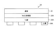
図3は、EUV吸収層をTaで構成し、DUV吸収層をCrで構成した場合のマスクの構成を示す図である。図3では、マスク2Xの一例であるマスク2Aの断面構成を示している。マスク2Aでは、基板21上に、EUV反射層22Xの一例であるMoSi(モリブデンシリサイド)多層膜22Aが積層されている。さらに、MoSi多層膜22Aの上層側には、DUV反射/EUV吸収層23Xの一例であるTa層23Aが積層されている。そして、Ta層23Aの上層側には、吸収層24Xの一例であるCr層24Aが積層されている。マスク2Aでは、Cr層24Aを用いて露光量モニターパターンが形成されている。
FIG. 3 is a diagram showing a mask configuration when the EUV absorption layer is made of Ta and the DUV absorption layer is made of Cr. FIG. 3 shows a cross-sectional configuration of a
図4は、DUV反射/EUV吸収層におけるDUV光の反射率特性を示す図である。図4に示すグラフの横軸は、マスク2A(マスク2X)上の座標であり、縦軸は、マスク2A(マスク2X)での反射率である。Ta層23A(DUV反射/EUV吸収層23X)およびCr層24A(吸収層24X)では、EUV光を吸収する。したがって、EUV光の反射率特性Eは、マスク2A上の全面で略0となる。
FIG. 4 is a diagram showing the reflectance characteristics of DUV light in the DUV reflection / EUV absorption layer. The horizontal axis of the graph shown in FIG. 4 is the coordinates on the
一方、DUV光は、Ta層23Aで反射され、Cr層24Aで吸収される。したがって、DUV光の反射率特性Dは、Ta層23Aに対応する位置では所定値を示し、Cr層24Aに対応する位置では略0となる。
On the other hand, the DUV light is reflected by the
これにより、マスク2AにEUV光が照射されても、ウエハ20にはEUV光が照射されない。一方、Ta層23Aに対応する位置で反射されたDUV光は、ウエハ20上に照射される。したがって、Cr層24Aの有無に応じた反射率のパターン分布をウエハ20上に形成することが可能となる。
Thereby, even if EUV light is irradiated to the
図5は、露光量モニターパターンを説明するための図である。露光量モニターパターン5は、ウエハ20上に照射されるDUV光の光強度(露光量)を測定するためのマスクパターンである。図5の(a)に示すように、露光量モニターパターン5は、ライン&スペースパターンで構成されている。ライン&スペースパターンは、ラインパターンとスペースパターン(スペース領域)とが、所定の周期で交互に配置されたパターンである。露光量モニターパターン5のライン&スペースパターンは、パターンピッチが同じでラインパターンとスペースパターンのデューティ比が少しずつ変化するよう構成されている。
FIG. 5 is a diagram for explaining an exposure amount monitor pattern. The exposure
具体的には、露光量モニターパターン5の左端部および右端部には、ラインパターンの幅に対してスペースパターンの幅が広い(デューティ比が大きい)ライン&スペースパターンが配置されている。そして、露光量モニターパターン5の中心部に近づくに従って、デューティ比が小さいライン&スペースパターンが配置されている。これにより、露光量モニターパターン5の左端部および右端部には、最も大きなデューティ比のライン&スペースパターンが配置され、露光量モニターパターン5の中心部には、最も小さなデューティ比のライン&スペースパターンが配置されている。
Specifically, a line & space pattern in which the width of the space pattern is wider (the duty ratio is large) than the width of the line pattern is arranged at the left end and the right end of the exposure
EUV光よりも長い波長領域で検出対象となる波長領域(DUV領域)の中心波長をλとし、EUV露光装置1の投影光学系開口数をNAとし、有効光源の大きさをσとした場合、露光量モニターパターン5のラインパターンとスペースパターンとが配置される周期(ピッチ)Pとして、以下の式(1)で示される値を設定する。
P<λ/{(1+σ)NA}・・・(1)
When the center wavelength of the wavelength region (DUV region) to be detected in the wavelength region longer than EUV light is λ, the projection optical system numerical aperture of the
P <λ / {(1 + σ) NA} (1)
露光量モニターパターン5にEUV光およびDUV光を照射すると、露光量モニターパターン5ではDUV光の一部が反射されてウエハ20に照射される。ウエハ20に照射されるDUV光は、露光量モニターパターン5のパターン形状に応じた光強度を有している。
When the exposure
図5の(b)に示すグラフの横軸は、露光量モニターパターン5上での座標であり、縦軸は、ウエハ20上での光強度である。同図に示すように、露光量モニターパターン5のうちデューティ比の大きな位置では、光強度が小さくなり、デューティ比の小さな位置では、光強度が大きくなる。
The horizontal axis of the graph shown in FIG. 5B is the coordinates on the exposure
具体的には、露光量モニターパターン5の左端部および右端部(デューティ比が最大の位置)に対応するウエハ20上の位置では、光強度が最小となる。そして、露光量モニターパターン5の中心部に対応するウエハ20上の位置に近づくに従って、光強度が大きくなる。これにより、露光量モニターパターン5の中心部(デューティ比が最小の位置)に対応するウエハ20上の位置では、光強度が最大となる。本設定条件下では、少なくともDUV光領域における光強度分布は、露光時のフォーカス変動に対して非常に感度が低くなることが知られている。この為、露光領域内のDUV露光量分布を本露光量モニターパターンで、他のプロセス変動要因から切り離して高精度に評価することが可能となる。
Specifically, the light intensity is minimum at the position on the
なお、露光量モニターパターン5を複数パターン準備しておき、各露光量モニターパターン5に種々の被覆率を有した周辺パターンを配置してもよい。これにより、被覆率に応じたDUV光の光強度を評価することが可能となる。
A plurality of exposure
EUV露光装置1によってウエハ20上に照射されるDUV光を評価する際には、ウエハ20上に予めEUVレジストを塗布しておく。そして、マスク2Aを用いてウエハ20に露光光Lを照射し、その後、ウエハ20を現像する。これにより、フォーカス位置に鈍感なDUV転写像(転写パターン)がウエハ20上に形成される。この後、DUV転写像のパターン形状に基づいて、ウエハ20上へのDUV光の露光量が求められる。
When the DUV light irradiated onto the
例えば、DUV光の露光量と、ウエハ上に形成されるDUV転写像のパターン形状との相関関係を予め取得しておく。そして、この相関関係と、ウエハ20上に形成されたDUV転写像のパターン形状に基づいて、DUV光の露光量が求められる。これにより、DUV光領域の露光量分布を定量的に評価することが可能となる。
For example, the correlation between the exposure amount of DUV light and the pattern shape of the DUV transfer image formed on the wafer is acquired in advance. Based on this correlation and the pattern shape of the DUV transfer image formed on the
なお、露光量評価用のマスク(マスク2X,2A、後述するマスク2B)と、製品ウエハを露光するに用いる製品マスクとは、DUV光の反射率やEUV光の反射率が異なる場合がある。このような場合には、露光量評価用のマスクと、製品マスクとの間の、反射率(DUV光やEUV光の反射率)の差を考慮して、製品ウエハに照射されるDUV光の露光量を求めてもよい。換言すると、露光量評価用のマスクと、製品マスクとの間の、反射率の差に基づいて、求めたウエハ20上へのDUV光の露光量を補正し、これにより、製品ウエハに照射されるDUV光の露光量を求めてもよい。
Note that the exposure dose evaluation masks (
ウエハ20上に照射されるDUV光の露光量を求めた後には、この露光量測定の際に形成したウエハ20上のパターン形状と、以降の定期検査時などの際に形成するウエハ20上のパターン形状と、を比較することによって、DUV光の露光量変動を検査してもよい。
After the exposure amount of the DUV light irradiated on the
なお、本実施の形態では、ウエハ20上にパターンを形成した後にDUV光の露光量を求めたが、ウエハ20上にパターンを形成することなくDUV光の露光量を求めてもよい。この場合、例えば、CCD(Charge Coupled Device)センサーや、その他の受光素子等を用いて、ウエハ20上に照射されるDUV光の露光量を検出してもよい。
In the present embodiment, the exposure amount of the DUV light is obtained after the pattern is formed on the
なお、本実施の形態では、マスク2AがDUV光をCr層24Aで吸収する構成としたが、DUV光をCr層24A以外の層(例えば、基板21)で吸収させてもよい。図6は、DUV光を基板で吸収する場合のマスクの構成を示す図である。図6では、マスク2Bの断面構成を示している。
In the present embodiment, the
マスク2Bは、基板21上に、EUV反射層22Xの一例であるMoSi多層膜22Bが積層されている。基板21は、DUV光およびEUV光に対して低反射性の部材(例えば、透明部材)で構成しておく。MoSi多層膜22Bの上層側には、DUV反射/EUV吸収層23Xの一例であるTa層23Bが積層されている。そして、マスク2Bでは、MoSi多層膜22BおよびTa層23Bを用いて露光量モニターパターン5が形成されている。マスク2Bでは、MoSi多層膜22BとTa層23Bに同じ形状のパターニングを行うことにより、露光量モニターパターン5が形成されている。
In the
露光量モニターパターンを形成する際には、電子ビーム描画装置などによってTa層23B上にレジストパターンが形成され、レジストパターン上からTa層23BおよびMoSi多層膜22Bがエッチングされる。
When the exposure amount monitor pattern is formed, a resist pattern is formed on the
このように、MoSi多層膜22BとTa層23Bを露光量モニターパターン形状に削り込んでおくことで、MoSi多層膜22Bが削り込まれた先の層(基板21)では、EUV光の反射率を略0にすることが可能となる。
In this way, by cutting the
マスク2Bに対して、Ta層23B側からEUV光を照射すると、Ta層23BではEUV光が吸収され、基板21では、EUV光を透過させる。一方、DUV光は、Ta層23Bで反射され、基板21ではDUV光を透過させる。したがって、Ta層23B、MoSi多層膜22Bに形成されているマスクパターン(露光量モニターパターン5)に応じたパターンがウエハ20上に転写される。
When the
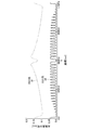
図7に転写像のシミュレーション結果を示す。図7は、図6に示したマスクにより得られる光強度分布シミュレーション結果を示す図である。図7に示すグラフは、横軸が座標であり、縦軸が光強度分布である。特性32は、EUV光(中心波長13.5nm)の光強度分布シミュレーション結果であり、特性31は、DUV光(中心波長199nm)の光強度分布シミュレーション結果である。シミュレーション条件としては、NA=0.25、σ=0.8を選択した。本条件では、EUVの反射光量がEUV吸収層に対応する箇所でも相対的に大きく、DUV光測定精度を劣化させることが懸念される。 FIG. 7 shows a simulation result of the transfer image. FIG. 7 is a diagram showing a light intensity distribution simulation result obtained by the mask shown in FIG. In the graph shown in FIG. 7, the horizontal axis represents coordinates, and the vertical axis represents light intensity distribution. A characteristic 32 is a light intensity distribution simulation result of EUV light (center wavelength 13.5 nm), and a characteristic 31 is a light intensity distribution simulation result of DUV light (center wavelength 199 nm). As simulation conditions, NA = 0.25 and σ = 0.8 were selected. Under this condition, the amount of reflected EUV light is relatively large even at a location corresponding to the EUV absorption layer, and there is a concern that the DUV light measurement accuracy may be degraded.
図8にEUV+DUV光の合成像と、300nmほどデフォーカスさせた位置での合成像結果を示す。図8は、図7に示した光強度分布の強度和計算結果を示す図である。図8に示すグラフは、横軸が座標であり、縦軸が光強度分布である。特性33は、EUV光強度とDUV光強度の強度和(EUV光とDUV光の合成像)であり、特性34は、EUV光とDUV光の合成像(デフォーカス)である。EUV光による像強度が変動して合成像にも影響を与えることがわかる。精度を上げるためにはEUV吸収層23BでのEUV光の反射率を低下させるために、23B上にEUV反射量を低下させる膜を追加形成する、あるいは23B膜厚を従来よりも厚く形成しておいてもよい。
FIG. 8 shows a composite image of EUV + DUV light and a composite image result at a position defocused by about 300 nm. FIG. 8 is a diagram illustrating the intensity sum calculation result of the light intensity distribution illustrated in FIG. 7. In the graph shown in FIG. 8, the horizontal axis represents coordinates, and the vertical axis represents light intensity distribution. A characteristic 33 is the sum of the EUV light intensity and the DUV light intensity (a composite image of EUV light and DUV light), and a characteristic 34 is a composite image (defocus) of the EUV light and DUV light. It can be seen that the image intensity due to EUV light fluctuates and affects the composite image. In order to increase accuracy, in order to reduce the reflectivity of EUV light in the
なお、マスク2Xの構成としては、EUV反射層22Xと、DUV反射/EUV吸収層23Xとの間にバッファ層を設けてもよい。また、本実施の形態では、マスク2XがEUV反射層22Xを有する構成としたが、マスク2Xは、EUV反射層22Xを有していなくてもよい。また、マスク2BがMoSi多層膜22Bを有する構成としたが、マスク2Bは、MoSi多層膜22Bを有していなくてもよい。
As a configuration of the
また、吸収層24Xは、Cr層24Aに限らず、C膜、Cr/CrO膜、CrN膜、SiO膜、SiN膜、Cr/F膜などのDUV光に対する低反射材を含む構成であってもよい。
Further, the
また、本実施の形態では、露光量モニターパターン5を、DUV光を吸収する吸収層24X(低反射材)で形成したが、露光量モニターパターン5を、DUV光を高反射率で反射する反射層、例えばRu膜、Si膜、Al膜等で形成してもよい。
In the present embodiment, the exposure
換言すると、露光量モニターパターン5は、DUV光の反射率が異なる2種類の膜を用いて形成しておけばよい。例えば、マスク2Xの場合、DUV反射/EUV吸収層23Xの位置に第1のDUV光反射率を有した膜を積層し、この膜の上層側(吸収層24Xの位置)に第2のDUV光反射率を有した露光量モニターパターン5を形成しておく。
In other words, the exposure
また、マスク2Bの場合、基板21を第3のDUV光反射率を有した部材で構成し、この部材の上層側(Ta23Bの位置)に第4のDUV光反射率を有した露光量モニターパターン5を形成しておく。
In the case of the
ここでの第1のDUV光反射率と、第2のDUV光反射率との差は、例えば15%以上である。また、第3のDUV光反射率と、第4のDUV光反射率との差は、例えば15%以上である。 Here, the difference between the first DUV light reflectance and the second DUV light reflectance is, for example, 15% or more. Further, the difference between the third DUV light reflectance and the fourth DUV light reflectance is, for example, 15% or more.
例えば、Ta膜のDUV反射率は19%であり、ガラス基板のDUV反射率は4%である。また、CrN膜のDUV反射率は18%であり、Ru膜のDUV反射率は67%であり、Si膜のDUV反射率は54%である。露光量モニターパターン5は、このような種々のDUV反射率を有した膜層の組み合わせを用いて形成される。
For example, the DUV reflectance of the Ta film is 19%, and the DUV reflectance of the glass substrate is 4%. The CrN film has a DUV reflectance of 18%, the Ru film has a DUV reflectance of 67%, and the Si film has a DUV reflectance of 54%. The exposure
また、第1のDUV光反射率を有した膜でのEUV光反射率と、露光量モニターパターン5でのEUV光反射率との差は、小さいほどよい。また、基板21でのEUV光反射率と、露光量モニターパターン5でのEUV光反射率との差は、小さいほどよい。
Further, the smaller the difference between the EUV light reflectance in the film having the first DUV light reflectance and the EUV light reflectance in the exposure
また、DUV反射/EUV吸収層23Xは、EUV光を吸収する層に限らず、EUV光を透過させる層であってもよい。また、基板21は、DUV光やEUV光を透過させる部材に限らず、DUV光やEUV光を吸収する部材で構成してもよい。
The DUV reflection /
DUV光領域の露光量分布を求めた後、露光量分布に基づいて、Outband成分による露光の影響を含めたパターン転写予測を行うことが可能となる。パターン転写予測を行う際には、DUV光領域の露光量分布に基づいてEUVフレア計算などを行うことで、高精度なパターン転写予測を行うことが可能となる。また、パターン転写予測の予測結果に基づいて、マスクパターン(設計パターン)の補正を行うことが可能となる。 After obtaining the exposure amount distribution in the DUV light region, it is possible to perform pattern transfer prediction including the influence of exposure by the Outband component based on the exposure amount distribution. When performing pattern transfer prediction, it is possible to perform highly accurate pattern transfer prediction by performing EUV flare calculation or the like based on the exposure amount distribution in the DUV light region. Further, it is possible to correct the mask pattern (design pattern) based on the prediction result of the pattern transfer prediction.
必要に応じてマスクパターンが補正された後、製品マスクを用いて半導体装置(半導体集積回路)が製造される。製品マスクは、基板上にEUV光の反射層が形成され、EUV光の反射層上にEUV光の吸収層が形成されている。そして、EUV光の吸収層に回路パターンが形成されている。 After the mask pattern is corrected as necessary, a semiconductor device (semiconductor integrated circuit) is manufactured using the product mask. In the product mask, an EUV light reflection layer is formed on a substrate, and an EUV light absorption layer is formed on the EUV light reflection layer. A circuit pattern is formed on the EUV light absorption layer.
半導体装置を製造する際には、製品マスクがEUV露光装置1にセットされる。そして、レジストの塗布されたウエハに製品マスクを用いて製品ウエハへの露光が行なわれる。製品マスクに対して、EUV光の吸収層側からEUV光を照射すると、EUV光の吸収層では、EUV光が吸収され、EUV光の反射層ではEUV光が反射される。したがって、EUV光の吸収層を用いて形成されている回路パターンに応じたパターンが製品ウエハ上に転写される。
When manufacturing a semiconductor device, a product mask is set in the
この後、製品ウエハが現像されて製品ウエハ上にレジストパターンが形成される。そして、レジストパターンをマスクとしてレジストパターンの下層側がエッチングされる。これにより、レジストパターンに対応する実パターンが製品ウエハ上に形成される。半導体装置を製造する際には、上述したマスクパターンの補正処理、露光処理、現像処理、エッチング処理などがレイヤ毎に行われる。 Thereafter, the product wafer is developed to form a resist pattern on the product wafer. Then, the lower layer side of the resist pattern is etched using the resist pattern as a mask. Thereby, an actual pattern corresponding to the resist pattern is formed on the product wafer. When manufacturing a semiconductor device, the above-described mask pattern correction processing, exposure processing, development processing, etching processing, and the like are performed for each layer.
このように実施の形態によれば、DUV光の反射率差を有した少なくとも2種類の膜を用いて露光量モニターパターンを形成しているので、EUV光以外の波長を有した露光光を容易に評価することが可能となる。したがって、EUV露光装置1を用いてEUV露光した際の、製品ウエハ上でのパターン転写特性を精度良く予測することが可能となる。
As described above, according to the embodiment, since the exposure amount monitor pattern is formed using at least two kinds of films having a reflectance difference of DUV light, exposure light having a wavelength other than EUV light can be easily obtained. It becomes possible to evaluate. Therefore, it is possible to accurately predict the pattern transfer characteristics on the product wafer when EUV exposure is performed using the
本発明のいくつかの実施形態を説明したが、これらの実施形態は、例として提示したものであり、発明の範囲を限定することは意図していない。これら新規な実施形態は、その他の様々な形態で実施されることが可能であり、発明の要旨を逸脱しない範囲で、種々の省略、置き換え、変更を行うことができる。これら実施形態やその変形は、発明の範囲や要旨に含まれるとともに、特許請求の範囲に記載された発明とその均等の範囲に含まれる。 Although several embodiments of the present invention have been described, these embodiments are presented by way of example and are not intended to limit the scope of the invention. These novel embodiments can be implemented in various other forms, and various omissions, replacements, and changes can be made without departing from the scope of the invention. These embodiments and modifications thereof are included in the scope and gist of the invention, and are included in the invention described in the claims and the equivalents thereof.
1…EUV露光装置、2A,2B,2X…マスク、5…露光量モニターパターン、20…ウエハ、21…基板、22A,22B…MoSi多層膜、22X…EUV反射層、23A,23B…Ta層、23X…DUV反射/EUV吸収層、24A…Cr層、24X…吸収層。
DESCRIPTION OF
Claims (9)
前記フォトマスクに対し前記マスクパターン側から前記露光光を照射するとともに、前記フォトマスクで反射された露光光を前記基板に照射する照射ステップと、
前記基板に照射された露光光の露光量に基づいて、前記基板に照射された長波長光の光量分布を測定する光量測定ステップと、
を含むことを特徴とする露光量評価方法。 A long-wavelength light reflecting film that reflects long-wavelength light having a wavelength longer than EUV light and absorbs the EUV light, and an EUV light that is disposed on the upper layer side of the long-wavelength light reflecting film. A set step of setting a photomask having a mask pattern formed using an absorption film that absorbs the long-wavelength light, and a substrate to be exposed coated with a resist, in an EUV exposure apparatus;
Irradiating the substrate with the exposure light reflected from the photomask and irradiating the photomask from the mask pattern side;
A light amount measuring step for measuring a light amount distribution of the long wavelength light irradiated to the substrate based on an exposure amount of the exposure light irradiated to the substrate;
The exposure amount evaluation method characterized by including.
前記フォトマスクに対し前記マスクパターン側から前記露光光を照射するとともに、前記フォトマスクで反射された露光光を前記基板に照射する照射ステップと、
前記基板に照射された露光光の露光量に基づいて、前記基板に照射された長波長光の光量分布を測定する光量測定ステップと、
を含むことを特徴とする露光量評価方法。 Of the exposure light, long wavelength light having a longer wavelength than EUV light and an absorption film that absorbs the EUV light, and an upper layer side of the absorption film that absorbs the EUV light and absorbs the long wavelength light. A set step of setting a photomask having a mask pattern formed by using a reflective long wavelength light reflecting film and a substrate to be exposed coated with a resist in an EUV exposure apparatus;
Irradiating the substrate with the exposure light reflected from the photomask and irradiating the photomask from the mask pattern side;
A light amount measuring step for measuring a light amount distribution of the long wavelength light irradiated to the substrate based on an exposure amount of the exposure light irradiated to the substrate;
The exposure amount evaluation method characterized by including.
前記光量測定ステップは、前記転写パターンのパターン形状に基づいて、前記基板に照射された長波長光の光量分布を測定することを特徴とする請求項1または2に記載の露光量評価方法。 A transfer pattern forming step of forming a transfer pattern corresponding to the mask pattern on the substrate by developing the substrate irradiated with the exposure light reflected by the photomask;
The exposure amount evaluation method according to claim 1, wherein the light amount measurement step measures a light amount distribution of the long wavelength light irradiated on the substrate based on a pattern shape of the transfer pattern.
露光光のうちEUV光よりも長い波長を有した長波長光の露光量の評価に用いられるとともに、
前記EUV光に対して反射性を有するマスク基板の上層に、
前記長波長光を反射し且つ前記EUV光を吸収する長波長光反射膜と、
前記長波長光反射膜の上層側に配置されるとともに前記EUV光および前記長波長光を吸収する吸収膜を用いて形成されたマスクパターンと、
が形成されていることを特徴とする反射型基板。 A reflective substrate that can be mounted at a reflective mask position of an EUV exposure apparatus,
Used to evaluate the exposure amount of long wavelength light having a longer wavelength than EUV light among exposure light,
On the upper layer of the mask substrate having reflectivity with respect to the EUV light,
And long wavelength light reflecting film for absorbing the reflected and the EUV light the long wavelength light,
A mask pattern formed on the upper layer side of the long-wavelength light reflecting film and formed using an absorption film that absorbs the EUV light and the long-wavelength light;
A reflective substrate characterized in that is formed.
露光光のうちEUV光よりも長い波長を有した長波長光の露光量の評価に用いられるとともに、
前記長波長光および前記EUV光を吸収する基板の上層に、
前記EUV光に対して反射性を有する膜で形成されたマスクパターンと、
前記反射膜で形成されたマスクパターンの上層側に配置されるとともに前記EUV光を吸収し且つ前記長波長光を反射する長波長光反射膜と、
が形成されていることを特徴とする反射型基板。 A reflective substrate that can be mounted at a reflective mask position of an EUV exposure apparatus,
Used to evaluate the exposure amount of long wavelength light having a longer wavelength than EUV light among exposure light,
On the upper layer of the substrate that absorbs the long wavelength light and the EUV light,
A mask pattern formed of a film having reflectivity with respect to the EUV light;
A long-wavelength light reflecting film disposed on the upper layer side of the mask pattern formed of the reflecting film and absorbing the EUV light and reflecting the long-wavelength light;
A reflective substrate characterized in that is formed.
Priority Applications (3)
| Application Number | Priority Date | Filing Date | Title |
|---|---|---|---|
| JP2010252134A JP5657352B2 (en) | 2010-11-10 | 2010-11-10 | Exposure amount evaluation method and reflection type substrate |
| US13/237,736 US9110374B2 (en) | 2010-11-10 | 2011-09-20 | Exposure amount evaluation method and photomask |
| US14/795,923 US9250512B2 (en) | 2010-11-10 | 2015-07-10 | Exposure amount evaluation method and photomask |
Applications Claiming Priority (1)
| Application Number | Priority Date | Filing Date | Title |
|---|---|---|---|
| JP2010252134A JP5657352B2 (en) | 2010-11-10 | 2010-11-10 | Exposure amount evaluation method and reflection type substrate |
Publications (2)
| Publication Number | Publication Date |
|---|---|
| JP2012104670A JP2012104670A (en) | 2012-05-31 |
| JP5657352B2 true JP5657352B2 (en) | 2015-01-21 |
Family
ID=46018715
Family Applications (1)
| Application Number | Title | Priority Date | Filing Date |
|---|---|---|---|
| JP2010252134A Expired - Fee Related JP5657352B2 (en) | 2010-11-10 | 2010-11-10 | Exposure amount evaluation method and reflection type substrate |
Country Status (2)
| Country | Link |
|---|---|
| US (2) | US9110374B2 (en) |
| JP (1) | JP5657352B2 (en) |
Families Citing this family (3)
| Publication number | Priority date | Publication date | Assignee | Title |
|---|---|---|---|---|
| DE102014216121A1 (en) * | 2014-08-13 | 2016-02-18 | Carl Zeiss Smt Gmbh | Mask for EUV lithography, EUV lithography equipment and method for determining a contrast fraction caused by DUV radiation |
| US10935673B2 (en) * | 2016-11-15 | 2021-03-02 | Asml Netherlands B.V. | Radiation analysis system |
| JP7506114B2 (en) | 2022-07-01 | 2024-06-25 | アルバック成膜株式会社 | MANUFACTURING METHOD OF MASK BLANKS, MASK BLANKS, AND PHOTOMASK |
Family Cites Families (18)
| Publication number | Priority date | Publication date | Assignee | Title |
|---|---|---|---|---|
| JPH04151818A (en) * | 1990-10-16 | 1992-05-25 | Canon Inc | Manufacture of mask structure for lithography use |
| JP3250415B2 (en) * | 1995-04-28 | 2002-01-28 | 凸版印刷株式会社 | Manufacturing method of halftone type phase shift mask |
| JP3302926B2 (en) | 1998-07-02 | 2002-07-15 | 株式会社東芝 | Inspection method for exposure equipment |
| JP3674591B2 (en) | 2002-02-25 | 2005-07-20 | ソニー株式会社 | Exposure mask manufacturing method and exposure mask |
| EP1426824A1 (en) * | 2002-12-04 | 2004-06-09 | ASML Netherlands B.V. | Lithographic apparatus, device manufacturing method, and device manufactured thereby |
| WO2005008754A1 (en) * | 2003-07-18 | 2005-01-27 | Nikon Corporation | Flare measurement method, exposure method, and flare measurement mask |
| US7034923B2 (en) | 2004-01-21 | 2006-04-25 | Asml Netherlands B.V. | Optical element, lithographic apparatus comprising such optical element and device manufacturing method |
| JP4635610B2 (en) * | 2005-01-07 | 2011-02-23 | 凸版印刷株式会社 | Reflective photomask blank, reflective photomask, and reflective photomask manufacturing method |
| JP2006237184A (en) * | 2005-02-24 | 2006-09-07 | Sony Corp | Mask correction method and mask for exposure |
| JP2007206333A (en) * | 2006-02-01 | 2007-08-16 | Elpida Memory Inc | Mask for measuring flare and method for measuring flare |
| JP2008041740A (en) | 2006-08-02 | 2008-02-21 | Toppan Printing Co Ltd | Reflective photo-mask blank, reflective photo-mask and exposure method for extreme ultraviolet ray |
| JP2008198788A (en) * | 2007-02-13 | 2008-08-28 | Toshiba Corp | Method of forming resist pattern |
| US8018578B2 (en) * | 2007-04-19 | 2011-09-13 | Asml Netherlands B.V. | Pellicle, lithographic apparatus and device manufacturing method |
| JP5018212B2 (en) * | 2007-04-26 | 2012-09-05 | 凸版印刷株式会社 | Reflective photomask blank, reflective photomask, and semiconductor device manufacturing method |
| NL1036695A1 (en) | 2008-05-15 | 2009-11-17 | Asml Netherlands Bv | Lithographic apparatus. |
| US8399159B2 (en) * | 2008-11-26 | 2013-03-19 | Hoya Corporation | Mask blank substrate |
| JP5330019B2 (en) * | 2009-02-18 | 2013-10-30 | ルネサスエレクトロニクス株式会社 | Mask pattern inspection method and mask pattern inspection apparatus |
| JP5397596B2 (en) * | 2009-03-03 | 2014-01-22 | 株式会社ニコン | Flare measurement method and exposure method |
-
2010
- 2010-11-10 JP JP2010252134A patent/JP5657352B2/en not_active Expired - Fee Related
-
2011
- 2011-09-20 US US13/237,736 patent/US9110374B2/en active Active
-
2015
- 2015-07-10 US US14/795,923 patent/US9250512B2/en active Active
Also Published As
| Publication number | Publication date |
|---|---|
| JP2012104670A (en) | 2012-05-31 |
| US9110374B2 (en) | 2015-08-18 |
| US20150331308A1 (en) | 2015-11-19 |
| US9250512B2 (en) | 2016-02-02 |
| US20120112085A1 (en) | 2012-05-10 |
Similar Documents
| Publication | Publication Date | Title |
|---|---|---|
| US7327436B2 (en) | Method for evaluating a local flare, correction method for a mask pattern, manufacturing method for a semiconductor device and a computer program product | |
| US7376512B2 (en) | Method for determining an optimal absorber stack geometry of a lithographic reflection mask | |
| US11487198B2 (en) | Patterning device, a method of making the same, and a patterning device design method | |
| JP4339841B2 (en) | Lithographic apparatus and device manufacturing method | |
| KR100541487B1 (en) | Adjustment method and apparatus of optical system, and exposure apparatus | |
| JP2007329368A (en) | Multilayer film mirror, evaluation method, exposure apparatus, and device manufacturing method | |
| JP7535577B2 (en) | Method for determining the optical phase difference of a measurement light of a measurement light wavelength across a surface of a structured object - Patents.com | |
| JP2011517126A (en) | Diffraction element for alignment target | |
| KR101713382B1 (en) | An extreme ultraviolet lithography process and mask | |
| JP2009272347A (en) | Light reflecting mask, exposure apparatus, measuring method, and method of manufacturing semiconductor device | |
| US9250512B2 (en) | Exposure amount evaluation method and photomask | |
| US6627356B2 (en) | Photomask used in manufacturing of semiconductor device, photomask blank, and method of applying light exposure to semiconductor wafer by using said photomask | |
| Mailfert et al. | 3D mask modeling for EUV lithography | |
| CN114303102A (en) | Assembly for collimating broadband radiation | |
| JP6609307B2 (en) | EUV lithographic mask, EUV lithographic apparatus, and method for determining contrast ratio due to DUV radiation | |
| KR101791729B1 (en) | Method and system for reducing pole imbalance by adjusting exposure intensity | |
| Tirapu-Azpiroz et al. | Understanding the trade-offs of thinner binary mask absorbers | |
| US11226551B2 (en) | Lithographic mask, a pellicle therein and method of forming the same | |
| CN113557477B (en) | Lithographic apparatus, metrology apparatus, optical system and method | |
| KR101069433B1 (en) | Method for correcting pattern CD of mask for extreme ultraviolet lithography | |
| KR20130006747A (en) | Blank euv photomask and method of fabricating a euv photomask using the same | |
| Lee et al. | Multistack structure for an extreme-ultraviolet pellicle with out-of-band radiation reduction | |
| TW202422214A (en) | Suppressing specular reflection of mask absorber and on-resolution field stitching | |
| JP2004134444A (en) | Method and instrument for measuring optical characteristic of optical system for extremely-short ultraviolet ray and method of manufacturing the optical system | |
| JP2010205886A (en) | Method for evaluating flare of exposure device |
Legal Events
| Date | Code | Title | Description |
|---|---|---|---|
| A621 | Written request for application examination |
Free format text: JAPANESE INTERMEDIATE CODE: A621 Effective date: 20130220 |
|
| A977 | Report on retrieval |
Free format text: JAPANESE INTERMEDIATE CODE: A971007 Effective date: 20131113 |
|
| A131 | Notification of reasons for refusal |
Free format text: JAPANESE INTERMEDIATE CODE: A131 Effective date: 20131126 |
|
| A521 | Request for written amendment filed |
Free format text: JAPANESE INTERMEDIATE CODE: A523 Effective date: 20131226 |
|
| A131 | Notification of reasons for refusal |
Free format text: JAPANESE INTERMEDIATE CODE: A131 Effective date: 20140729 |
|
| A521 | Request for written amendment filed |
Free format text: JAPANESE INTERMEDIATE CODE: A523 Effective date: 20140924 |
|
| TRDD | Decision of grant or rejection written | ||
| A01 | Written decision to grant a patent or to grant a registration (utility model) |
Free format text: JAPANESE INTERMEDIATE CODE: A01 Effective date: 20141028 |
|
| A61 | First payment of annual fees (during grant procedure) |
Free format text: JAPANESE INTERMEDIATE CODE: A61 Effective date: 20141126 |
|
| R151 | Written notification of patent or utility model registration |
Ref document number: 5657352 Country of ref document: JP Free format text: JAPANESE INTERMEDIATE CODE: R151 |
|
| S111 | Request for change of ownership or part of ownership |
Free format text: JAPANESE INTERMEDIATE CODE: R313111 |
|
| R350 | Written notification of registration of transfer |
Free format text: JAPANESE INTERMEDIATE CODE: R350 |
|
| S111 | Request for change of ownership or part of ownership |
Free format text: JAPANESE INTERMEDIATE CODE: R313111 |
|
| R350 | Written notification of registration of transfer |
Free format text: JAPANESE INTERMEDIATE CODE: R350 |
|
| LAPS | Cancellation because of no payment of annual fees |