JP5651990B2 - Digital coherent receiver and receiving method - Google Patents
Digital coherent receiver and receiving method Download PDFInfo
- Publication number
- JP5651990B2 JP5651990B2 JP2010094436A JP2010094436A JP5651990B2 JP 5651990 B2 JP5651990 B2 JP 5651990B2 JP 2010094436 A JP2010094436 A JP 2010094436A JP 2010094436 A JP2010094436 A JP 2010094436A JP 5651990 B2 JP5651990 B2 JP 5651990B2
- Authority
- JP
- Japan
- Prior art keywords
- unit
- frequency offset
- digital signal
- spectrum
- signal
- Prior art date
- Legal status (The legal status is an assumption and is not a legal conclusion. Google has not performed a legal analysis and makes no representation as to the accuracy of the status listed.)
- Active
Links
Images

Classifications
-
- H—ELECTRICITY
- H04—ELECTRIC COMMUNICATION TECHNIQUE
- H04B—TRANSMISSION
- H04B10/00—Transmission systems employing electromagnetic waves other than radio-waves, e.g. infrared, visible or ultraviolet light, or employing corpuscular radiation, e.g. quantum communication
- H04B10/60—Receivers
- H04B10/61—Coherent receivers
- H04B10/616—Details of the electronic signal processing in coherent optical receivers
- H04B10/6164—Estimation or correction of the frequency offset between the received optical signal and the optical local oscillator
-
- H—ELECTRICITY
- H04—ELECTRIC COMMUNICATION TECHNIQUE
- H04B—TRANSMISSION
- H04B10/00—Transmission systems employing electromagnetic waves other than radio-waves, e.g. infrared, visible or ultraviolet light, or employing corpuscular radiation, e.g. quantum communication
- H04B10/60—Receivers
- H04B10/61—Coherent receivers
- H04B10/65—Intradyne, i.e. coherent receivers with a free running local oscillator having a frequency close but not phase-locked to the carrier signal
-
- H—ELECTRICITY
- H04—ELECTRIC COMMUNICATION TECHNIQUE
- H04L—TRANSMISSION OF DIGITAL INFORMATION, e.g. TELEGRAPHIC COMMUNICATION
- H04L27/00—Modulated-carrier systems
- H04L27/18—Phase-modulated carrier systems, i.e. using phase-shift keying
- H04L27/22—Demodulator circuits; Receiver circuits
- H04L27/223—Demodulation in the optical domain
Landscapes
- Engineering & Computer Science (AREA)
- Computer Networks & Wireless Communication (AREA)
- Signal Processing (AREA)
- Physics & Mathematics (AREA)
- Electromagnetism (AREA)
- Optical Communication System (AREA)
Description
本発明は、光を受信するデジタルコヒーレント受信器および受信方法に関する。 The present invention relates to a digital coherent receiver and a receiving method for receiving light.
インターネットにおけるトラフィックの増大により、幹線系の光通信システムの大容量化が求められており、1波長あたり100[Gbit/s]を超える信号を伝送可能な光送受信器の研究開発が行われている。1波長あたりのビットレートを大きくすると、OSNR(Optical Signal Noise Ratio:光信号対雑音比)耐力の低下や、伝送路の波長分散、偏波モード分散もしくは非線形効果などによる波形歪による信号品質の劣化が大きくなる。 Due to the increase in traffic on the Internet, there is a need to increase the capacity of trunk optical communication systems, and research and development of optical transceivers capable of transmitting signals exceeding 100 [Gbit / s] per wavelength are being conducted. . When the bit rate per wavelength is increased, the OSNR (Optical Signal Noise Ratio) strength is reduced, and the signal quality is degraded due to waveform distortion due to wavelength dispersion, polarization mode dispersion, or non-linear effects in the transmission path. Becomes larger.
このため、近年、OSNR耐力および伝送路の波形歪耐力があるデジタルコヒーレント受信方式が検討されている。従来の光強度のオン/オフを2値信号に割り当てて直接検波する方式に対して、デジタルコヒーレント受信方式では、光強度と位相情報をコヒーレント受信方式により抽出する。そして、抽出された強度と位相情報をAD(Analog/Digital)変換器により量子化し、デジタル信号処理部によって復調を行う。 For this reason, in recent years, a digital coherent reception method having an OSNR tolerance and a waveform distortion tolerance of a transmission path has been studied. In contrast to the conventional method of directly detecting on / off of the light intensity by assigning the binary signal to the binary signal, in the digital coherent reception method, the light intensity and the phase information are extracted by the coherent reception method. The extracted intensity and phase information is quantized by an AD (Analog / Digital) converter, and demodulated by a digital signal processing unit.
デジタルコヒーレント受信器の利点の一つとして、送信光源と局部発信光源の周波数および位相を受信光に対して同期させるメカニズムをデジタル信号処理として実装できるという利点が挙げられる。これにより、実現難度の高い光PLL(Phase Locked Loop)を実装しなくても送信光源と局部発信光源の周波数および位相を受信光に対して同期させることができる。 One advantage of the digital coherent receiver is that a mechanism for synchronizing the frequency and phase of the transmission light source and the local light source with respect to the received light can be implemented as digital signal processing. This makes it possible to synchronize the frequency and phase of the transmission light source and the local transmission light source with respect to the reception light without mounting an optical PLL (Phase Locked Loop) that is difficult to realize.
一般的な波長多重用光源を用いる場合は、送信器側の光源と受信器側のLO光源(Local Oscillator)との間には、波長確度の範囲内で光周波数のズレ(周波数オフセット)が発生し得る。一般的な波長多重用光源の場合は、この周波数オフセットは最大で数[GHz]程度となる可能性がある。 When a general wavelength multiplexing light source is used, an optical frequency shift (frequency offset) occurs within the range of wavelength accuracy between the light source on the transmitter side and the LO light source (Local Oscillator) on the receiver side. Can do. In the case of a general wavelength multiplexing light source, there is a possibility that this frequency offset is several [GHz] at the maximum.
一例として、QPSK(Quadrature Phase Shift Keying:四位相偏移変調)の信号を受信する場合について説明する。周波数オフセットが十分小さい場合は、ある短時間にわたって観測した信号コンスタレーションには、位相ズレによる静的回転のみが観測される。一方、周波数オフセットが大きい場合は、周波数オフセットによって観測時間内にコンスタレーションが回転するため、そのままではQPSK信号の処理および識別が困難になる。このため、周波数オフセットの補償が用いられる。以後、送信光源とLO光源の周波数差だけでなく、周波数オフセットに起因する位相回転も周波数オフセットと呼ぶ。 As an example, a case where a QPSK (Quadrature Phase Shift Keying) signal is received will be described. When the frequency offset is sufficiently small, only the static rotation due to the phase shift is observed in the signal constellation observed over a short time. On the other hand, when the frequency offset is large, since the constellation rotates within the observation time due to the frequency offset, it becomes difficult to process and identify the QPSK signal as it is. For this reason, frequency offset compensation is used. Hereinafter, not only the frequency difference between the transmission light source and the LO light source, but also the phase rotation caused by the frequency offset is called a frequency offset.
周波数オフセットの補償のためには、たとえば、オフセット推定回路により周波数オフセットを推定し、推定した周波数オフセットの分だけコンスタレーションをデジタル回路内で逆回転させる。オフセット推定回路の例としては、たとえばm値のPSK信号をm乗することにより、複素電界情報から符号化成分と雑音成分を除去し、周波数オフセットの成分を抽出する技術が知られている(たとえば、下記非特許文献1参照。)。また、信号の仮判定を行い、仮判定の結果を差し引いて符号化成分を除去し、周波数オフセットの推定範囲を拡大する技術が知られている(たとえば、下記非特許文献2参照。)。
In order to compensate for the frequency offset, for example, the frequency offset is estimated by an offset estimation circuit, and the constellation is reversely rotated in the digital circuit by the estimated frequency offset. As an example of an offset estimation circuit, a technique is known in which, for example, an m-value PSK signal is raised to the power of m to remove a coding component and a noise component from complex electric field information and extract a frequency offset component (for example, (See Non-Patent
しかしながら、上述した従来技術では、周波数オフセットの推定回路には引き込みレンジの制限があり、引き込みレンジ外の周波数オフセットを精度よく推定することができない。このため、周波数オフセットを精度よく補償することができず、受信品質が低下するという問題がある。これに対して、差動デコードを用いることが考えられるが、差動デコードを用いると受信雑音耐力が低下するという問題がある。 However, in the above-described conventional technique, the frequency offset estimation circuit has a limit of the pull-in range, and the frequency offset outside the pull-in range cannot be accurately estimated. For this reason, there is a problem that the frequency offset cannot be accurately compensated and the reception quality is lowered. On the other hand, it is conceivable to use differential decoding, but if differential decoding is used, there is a problem in that reception noise resistance is reduced.
開示のデジタルコヒーレント受信器および受信方法は、上述した問題点を解消するものであり、受信品質を向上させることを目的とする。 The disclosed digital coherent receiver and reception method are intended to solve the above-described problems and to improve reception quality.
上述した課題を解決し、目的を達成するため、開示技術は、信号光と局発光とを用いて光電変換するフロントエンドと、前記フロントエンドの出力をデジタル信号に変換する変換部と、前記変換部によって変換されたデジタル信号のスペクトラム重心を算出する算出部と、前記算出部によって算出されたスペクトラム重心に基づいて前記デジタル信号の周波数オフセットを推定する推定部と、前記推定部によって推定された周波数オフセットに基づいて前記デジタル信号の周波数オフセットを小さくする調整部と、を備えることを要件とする。 In order to solve the above-described problems and achieve the object, the disclosed technology includes a front end that performs photoelectric conversion using signal light and local light, a conversion unit that converts an output of the front end into a digital signal, and the conversion A calculation unit that calculates a spectrum centroid of the digital signal converted by the unit, an estimation unit that estimates a frequency offset of the digital signal based on the spectrum centroid calculated by the calculation unit, and a frequency estimated by the estimation unit And an adjustment unit that reduces the frequency offset of the digital signal based on the offset.
開示のデジタルコヒーレント受信器および受信方法によれば、受信品質を向上させることができるという効果を奏する。 According to the disclosed digital coherent receiver and reception method, the reception quality can be improved.
以下に添付図面を参照して、開示技術の好適な実施の形態を詳細に説明する。開示技術は、デジタルコヒーレント受信器において、デジタル変換した信号のスペクトラム重心を用いることで、信号光と局発光との間の周波数オフセットを精度よく補償し、受信品質を向上させる。 Hereinafter, preferred embodiments of the disclosed technology will be described in detail with reference to the accompanying drawings. The disclosed technique uses a spectrum centroid of a digitally converted signal in a digital coherent receiver, thereby accurately compensating for a frequency offset between signal light and local light and improving reception quality.
(実施の形態1)
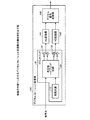
図1は、実施の形態1にかかるデジタルコヒーレント受信器の構成例を示す図である。図1に示すように、実施の形態1にかかるデジタルコヒーレント受信器100は、局発光源110と、光位相ハイブリッド回路120と、光電変換素子131,132と、AD変換器141,142と、デジタル信号処理部150と、を備えている。デジタルコヒーレント受信器100は、たとえばQPSKの信号光を受信する。
(Embodiment 1)
FIG. 1 is a diagram illustrating a configuration example of a digital coherent receiver according to the first embodiment. As shown in FIG. 1, the digital
局発光源110、光位相ハイブリッド回路120および光電変換素子131,132を含むフロントエンド10は、デジタルコヒーレント受信器100が受信する信号光と、局発光と、を混合して光電変換するフロントエンドである。具体的には、局発光源110は、局発光を生成し、生成した局発光を光位相ハイブリッド回路120へ出力する。局発光源110は、たとえばITLAである。
The
光位相ハイブリッド回路120は、信号光と、局発光源110から出力された局発光と、を混合することによって、光信号の光強度や位相を示す複素電界を抽出する。光位相ハイブリッド回路120は、抽出した複素電界の実部に応じた強度の光(I信号)を光電変換素子131へ出力する。また、光位相ハイブリッド回路120は、抽出した複素電界の虚部に応じた強度の光(Q信号)を光電変換素子132へ出力する。光位相ハイブリッド回路120の構成については、たとえば図2によって後述する。
The optical
光電変換素子131は、光位相ハイブリッド回路120から出力された光I信号を光電変換し、光電変換したI信号をAD変換器141へ出力する。光電変換素子132は、光位相ハイブリッド回路120から出力されたQ信号を光電変換し、光電変換したQ信号をAD変換器142へ出力する。光電変換素子131および光電変換素子132のそれぞれは、たとえばフォトダイオード(PD:Photo Diode)である。
The
AD変換器141,142は、フロントエンド10の出力をデジタル信号に変換する変換部である。具体的には、AD変換器141は、光電変換素子131から出力されたI信号を、所定のサンプリング周波数によって標本化することでデジタル信号に変換する。AD変換器142は、光電変換素子132から出力されたQ信号を、所定のサンプリング周波数によって標本化することでデジタル信号に変換する。AD変換器141,142のそれぞれは、デジタル信号に変換した信号をデジタル信号処理部150へ出力する。
The
デジタル信号処理部150は、AD変換器141,142から出力されたI信号およびQ信号のデジタル処理を行うことで信号光を識別する。デジタル信号処理部150は、信号光の識別結果を出力する。デジタル信号処理部150の構成については、たとえば図3によって後述する。
The digital
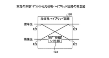
図2は、実施の形態1にかかる光位相ハイブリッド回路の概念図である。図2に示すように、光位相ハイブリッド回路120は、分岐部121,122と、90°位相シフト部123と、干渉部124,125と、を備えている。分岐部121には光信号が入力される。分岐部121は入力された信号光を分岐し、分岐した各信号光をそれぞれ干渉部124および干渉部125へ出力する。
FIG. 2 is a conceptual diagram of the optical phase hybrid circuit according to the first embodiment. As shown in FIG. 2, the optical
分岐部122には局発光源110からの局発光が入力される。分岐部122は、入力された局発光を分岐し、分岐した各局発光をそれぞれ干渉部124および90°位相シフト部123へ出力する。90°位相シフト部123は、分岐部122から出力された局発光の位相を90°シフトさせる。90°位相シフト部123は、位相をシフトさせた局発光を干渉部125へ出力する。
The local light from the local
干渉部124は、分岐部121から出力された信号光と、分岐部122から出力された局発光と、を干渉させる。干渉部124は、干渉させた光をI信号として光電変換素子131へ出力する。干渉部125は、分岐部121から出力された信号光と、90°位相シフト部123から出力された局発光と、を干渉させる。干渉部125は、干渉させた光をQ信号として光電変換素子132へ出力する。
The
図3は、実施の形態1にかかるデジタル信号処理部の構成例を示す図である。図3に示すように、デジタル信号処理部150は、フーリエ変換部151と、重心算出部152と、オフセット推定部153と、オフセット補償部154と、位相推定部155と、識別判定部156と、を備えている。デジタル信号処理部150には、たとえば、AD変換器141から出力されたI信号を実部とし、AD変換器142から出力されたQ信号を虚部とした複素数の信号が入力される。
FIG. 3 is a diagram of a configuration example of the digital signal processing unit according to the first embodiment. As shown in FIG. 3, the digital
フーリエ変換部151および重心算出部152は、AD変換器141,142によって変換された信号のスペクトラム重心を算出する算出部である。具体的には、フーリエ変換部151は、デジタル信号処理部150へ入力された信号をフーリエ変換(FFT:Fast Fourier Transform:高速フーリエ変換)する。フーリエ変換部151は、フーリエ変換により得られたスペクトラムを重心算出部152へ出力する。
The
重心算出部152は、フーリエ変換部151から出力されたスペクトラムの重心であるスペクトラム重心を算出する。スペクトラム重心は、たとえば、スペクトラムにおいて信号が分布している周波数範囲の中央の周波数である。重心算出部152は、たとえば下記(1)式によってスペクトラム重心を算出する。
The

上記(1)式において、iは、スペクトラムの周波数を示すインデックスである。P(i)は、インデックスiが示す周波数におけるスペクトラムのパワーである。Nは、フーリエ変換部151におけるフーリエ変換のFFTサイズである。Δは、fs/(N−1)である。fsは、AD変換器141,142におけるサンプリング周波数である。fbは、デジタルコヒーレント受信器100が受信する信号光のボーレートである。重心算出部152は、算出したスペクトラム重心をオフセット推定部153へ出力する。
In the above equation (1), i is an index indicating the frequency of the spectrum. P (i) is the power of the spectrum at the frequency indicated by index i. N is the FFT size of the Fourier transform in the
オフセット推定部153は、重心算出部152から出力されたスペクトラム重心に基づいて、デジタル信号処理部150へ入力された信号の周波数オフセットを推定する。オフセット推定部153は、周波数オフセットの推定結果を示すオフセット推定値をオフセット補償部154へ出力する。オフセット推定部153の構成については、たとえば図5によって後述する。
The offset
オフセット補償部154(調整部)は、オフセット推定部153から出力されたオフセット推定値に基づいて、デジタル信号処理部150へ入力された信号の周波数オフセットを補償する。たとえば、オフセット補償部154は、オフセット推定部153から出力されたオフセット推定値の逆特性を与えることで信号の周波数オフセットの補償を行う。ただし、オフセット補償部154による周波数オフセットの補償は、周波数オフセットを0にする場合に限らず、周波数オフセットを小さくするものであればよい。オフセット補償部154は、周波数オフセットを補償した信号を位相推定部155へ出力する。
The offset compensation unit 154 (adjustment unit) compensates for the frequency offset of the signal input to the digital
位相推定部155は、オフセット補償部154から出力された信号に対して、デジタルコヒーレント受信器100が受信した信号光と、局発光源110の局発光と、の間の位相差を推定して補償する。位相推定部155は、位相差を補償した信号を識別判定部156へ出力する。識別判定部156は、位相推定部155から出力された信号を識別する。識別判定部156は、識別結果を出力する。
The
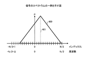
図4は、信号のスペクトラムの一例を示す図である。図4の横軸は、周波数およびインデックスiを示している。インデックスiは、周波数に対応するインデックスである。具体的には、インデックスiの−N/2+1〜N/2は、それぞれ周波数−fs/2+Δ〜fs/2に対応している。図4の縦軸は、周波数成分のパワーPを示している。スペクトラム400は、フーリエ変換部151から出力されたスペクトラムである。
FIG. 4 is a diagram illustrating an example of a spectrum of a signal. The horizontal axis in FIG. 4 indicates the frequency and the index i. The index i is an index corresponding to the frequency. Specifically, −N / 2 + 1 to N / 2 of the index i correspond to the frequencies −fs / 2 + Δ to fs / 2, respectively. The vertical axis in FIG. 4 indicates the power P of the frequency component. A
スペクトラム重心401は、重心算出部152によって算出されるスペクトラム重心である。スペクトラム重心401は、周波数オフセットの大きさに応じて0からずれる。したがって、オフセット推定部153は、スペクトラム重心401に基づいて周波数オフセットを推定することで、周波数オフセットを効率良く推定することができる。
The
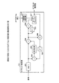
図5は、実施の形態1にかかるオフセット推定部の構成例を示す図である。図5に示すように、オフセット推定部153は、偏角算出部501と、減算部502と、仮判定部503と、減算部504と、遅延部505と、減算部506と、ループフィルタ507と、加算部508と、遅延部509と、初期値設定部510と、を備えている。
FIG. 5 is a diagram of a configuration example of the offset estimation unit according to the first embodiment. As illustrated in FIG. 5, the offset
図5に示すオフセット推定部153は、入力された信号の周波数オフセットを再帰的に推定する。すなわち、オフセット推定部153は、周波数オフセットの算出結果(ループフィルタ507の出力)をフィードバックしながら周波数オフセットを推定する。
The offset
オフセット推定部153へ入力された信号は、偏角算出部501へ入力される。偏角算出部501は、入力された複素数の信号が示す位相角を算出する。偏角算出部501は、算出した位相角を示す信号を減算部502および減算部504へ出力する。減算部502は、偏角算出部501から出力された信号から、遅延部509から出力された信号を減算する。減算部502は、減算結果を仮判定部503へ出力する。
The signal input to the offset
仮判定部503は、減算部502から出力された減算結果に基づいて信号を仮判定(識別)する。仮判定部503は、仮判定結果を示す信号を減算部504へ出力する。減算部504は、偏角算出部501から出力された信号から、仮判定部503から出力された信号を減算する。減算部504は、減算結果を示す信号を、遅延部505、減算部506および加算部508へ出力する。
The
遅延部505は、減算部504から出力された信号を1シンボル遅延させる。遅延部505は、遅延させた信号を減算部506へ出力する。減算部506は、遅延部505から出力された信号から、減算部504から出力された信号を減算する。減算部506は、減算結果を示す信号をループフィルタ507へ出力する。
The
ループフィルタ507は、減算部506から出力される信号を平均化する。たとえば、ループフィルタ507は、たとえば無限インパルス応答を有するIIR(Infinite Impulse Response)フィルタである。ループフィルタ507は、平均化した信号をオフセット推定値として出力する。また、ループフィルタ507は、平均化した信号を加算部508へ出力する。
The
加算部508は、減算部504から出力された信号と、ループフィルタ507から出力された信号と、を加算する。加算部508は、加算結果を示す信号を遅延部509へ出力する。遅延部509は、加算部508から出力された信号を1シンボル遅延させる。遅延部509は、遅延させた信号を減算部502へ出力する。
The
初期値設定部510は、重心算出部152から出力されたスペクトラム重心を、ループフィルタ507から出力される信号の初期値として設定する。このように、オフセット推定部153は、重心算出部152によって算出されたスペクトラム重心を初期値として、入力された信号の周波数オフセットを再帰的に推定する。
The initial
偏角算出部501から出力される時刻t+1の信号は位相角θ(t+1)を示す。位相角θ(t+1)は、θd(t+1)+θfo(t+1)+θPN(t+1)によって示すことができる。θd(t+1)は変調成分を示している。θfo(t+1)は周波数オフセットに起因する位相回転量を示している。θPN(t+1)は位相雑音を示している。
The signal at time t + 1 output from the deflection
また、仮判定部503から出力される信号は、変調成分の仮判定結果を示しているため、ほぼθd(t+1)となる。このため、減算部504から出力される信号は、θfo(t+1)+θPN(t+1)によって示すことができる。また、遅延部505から出力される信号は、θfo(t)+θPN(t)によって示すことができる。
Further, since the signal output from the
したがって、減算部506から出力される信号は、θfo(t+1)−θfo(t)+θPN(t+1)−θPN(t)によって示すことができる。θPN(t+1)=θPN(t)と見なすと、減算部506から出力される信号は、Δfo=θfo(t+1)−θfo(t)によって示すことができる。Δfoは、シンボル間の位相回転量の変化量であるため、周波数オフセットを示す。ループフィルタ507は、周波数オフセットΔfoを平均化することによってオフセット推定値を得ることができる。
Therefore, the signal output from the subtracting
また、加算部508から出力される信号は、θfo(t+1)+θPN(t+1)+Δfoとなる。したがって、遅延部509から出力される信号は、θfo(t)+θPN(t)+Δfoとなる。ここで、θfo(t)=θfo(t+1)−Δfoである。また、θPN(t)=θPN(t+1)と見なすことができる。このため、遅延部509から出力される信号は、θfo(t+1)+θPN(t+1)となる。したがって、減算部502から出力される信号は、変調成分θd(t+1)となる。
Further, the signal output from the adding
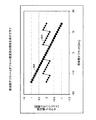
図6は、周波数オフセットとオフセット推定値の関係を示すグラフである。図6において、横軸は実際の周波数オフセット[GHz]を示している。縦軸はオフセット推定部153から出力されるオフセット推定値を示している。関係601は、ループフィルタ507の出力の初期値が固定値(たとえば0)と仮定した場合における、実際の周波数オフセットとオフセット推定値の関係を参考として示している。
FIG. 6 is a graph showing the relationship between the frequency offset and the offset estimated value. In FIG. 6, the horizontal axis represents the actual frequency offset [GHz]. The vertical axis represents the estimated offset value output from the offset
ループフィルタ507の出力の初期値を固定値とした場合(図6では0GHzとした)は、初期値と実際の周波数オフセットの差が大きくなると、周波数オフセットによる位相変化が位相変調による値の変化として誤認識される。このため、オフセット推定部153から出力されるオフセット推定値は、実際の周波数オフセットに対して周期的に変化する。このため、実際の周波数オフセットを正確に推定することができない。
When the initial value of the output of the
関係602は、ループフィルタ507の出力の初期値にスペクトラム重心を設定した場合における、実際の周波数オフセットに対するオフセット推定値の特性を示している。ループフィルタ507の出力の初期値にスペクトラム重心を設定することで、初期値を常に引き込みレンジ内にすることができるため、オフセット推定部153から出力されるオフセット推定値によって実際の周波数オフセットを得ることができる。
A
このように、実施の形態1にかかるデジタルコヒーレント受信器100によれば、信号のスペクトラム重心を用いて周波数オフセットを推定することができる。具体的には、周波数オフセットを再帰的に推定するオフセット推定部153において信号のスペクトラム重心を初期値として設定することで、信号光の受信時の周波数オフセットによらず、周波数オフセットを精度よく推定することができる(たとえば図6の関係602を参照)。
Thus, according to the digital
このため、周波数オフセットを精度よく補償し、受信品質を向上させることができる。また、周波数オフセットの引き込みレンジを拡大することができる。たとえば、差動デコードを用いなくても周波数オフセットの引き込みレンジを拡大することができる。このため、受信雑音耐力特性の低下を抑えつつ、受信品質を向上させることができる。 For this reason, it is possible to accurately compensate for the frequency offset and improve the reception quality. In addition, the frequency offset pull-in range can be expanded. For example, the frequency offset pull-in range can be expanded without using differential decoding. For this reason, it is possible to improve reception quality while suppressing a decrease in reception noise tolerance characteristics.
また、周波数オフセットを再帰的に推定するオフセット推定部153において信号のスペクトラム重心を初期値として設定することで、周波数オフセットの推定結果を短時間で収束させることができる。このため、デジタルコヒーレント受信器100の立ち上げ時間を短縮することができる。
Further, by setting the spectrum centroid of the signal as an initial value in the offset
(実施の形態2)
実施の形態2にかかるデジタルコヒーレント受信器100において、実施の形態1にかかるデジタルコヒーレント受信器100と同様の部分については説明を省略する。
(Embodiment 2)
In the digital
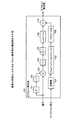
図7は、実施の形態2にかかるオフセット推定部の構成例を示す図である。図7に示すように、実施の形態2にかかるデジタルコヒーレント受信器100のオフセット推定部153は、遅延部701と、複素共役算出部702と、乗算部703と、累乗部704と、平均化部705と、偏角算出部706と、変換部707と、商演算部708と、演算部709と、加算部710と、を備えている。図7に示すオフセット推定部153は、入力された信号に基づいて算出した周波数オフセットを、重心算出部152によって算出されたスペクトラム重心に基づいて補正することで周波数オフセットを推定する。
FIG. 7 is a diagram of a configuration example of the offset estimation unit according to the second embodiment. As shown in FIG. 7, the offset
オフセット推定部153へ入力された信号(複素数)は、遅延部701および乗算部703へ入力される。遅延部701は、入力された信号を1シンボル遅延させ、遅延させた信号を複素共役算出部702へ出力する。複素共役算出部702は、遅延部701から出力された信号の複素共役を算出し、算出した複素共役を乗算部703へ出力する。
The signal (complex number) input to the offset
乗算部703は、オフセット推定部153へ入力された信号と、複素共役算出部702から出力された複素共役と、を乗算する。乗算部703による乗算結果は、オフセット推定部153へ入力された信号のシンボル間の位相差(位相回転量)を示す。ただし、乗算部703による乗算結果が示す位相回転量には、信号の変調成分による位相回転量と、周波数オフセットによる位相回転量と、が含まれている。乗算部703は、乗算結果を示す信号を累乗部704へ出力する。
累乗部704は、乗算部703から出力された信号をm乗する。mは、信号の1シンボルが示す値の数である。たとえば信号の変調方式がQPSKである場合は、累乗部704は信号を4乗する。これにより、乗算部703から出力された信号が示す位相回転量から、信号の変調成分による位相回転量を除去することができる。このため、累乗部704がm乗した信号は、周波数オフセットによる位相回転量(実際の位相回転量のm倍)を示す。累乗部704は、m乗した信号を平均化部705へ出力する。
The
平均化部705は、累乗部704から出力された信号をNサンプルずつ加算する。これにより、累乗部704から出力された信号の雑音を除去することができる。平均化部705は、加算結果を示す信号を偏角算出部706へ出力する。偏角算出部706は、平均化部705から出力された複素数の信号の偏角を算出し、算出した偏角をmで除算する。これにより、周波数オフセットを得ることができる。偏角算出部706は、算出した周波数オフセットをオフセット推定値として加算部710へ出力する。
The averaging
変換部707には、重心算出部152から出力されたスペクトラム重心が入力される。変換部707は、入力されたスペクトラム重心を1シンボル時間の位相回転量に変換する。変換部707は、変換した位相回転量xを商演算部708へ出力する。商演算部708は、変換部707から出力された位相回転量xにπ/mを加算した値を2π/mによって除算した商の整数部を演算する(FLOOR((x+π/m)/(2π/m)))。商演算部708は、演算結果を示す信号iを演算部709へ出力する。
The spectrum centroid output from the
演算部709は、商演算部708から出力された信号iに基づいて、−1*(2π/m)*iを演算する。演算部709は、演算結果をオフセット推定値の補正値として加算部710へ出力する。加算部710は、偏角算出部706から出力されたオフセット推定値と、偏角算出部706から出力された補正値と、を加算する。加算部710は、補正値を加算したオフセット推定値を出力する。
The
これにより、オフセット推定部153は、m値のPSKにおいて、スペクトラム重心によって推定される周波数オフセットに基づいて推定したオフセット推定値を補正することができる。このため、実際の周波数オフセットが推定範囲よりも大きくなり、実際の周波数オフセットに対してオフセット推定値が周期的に変化しても(たとえば図6の関係601を参照)、正確に周波数オフセットを推定することができる。
Thereby, the offset
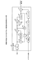
図8は、実施の形態2にかかるオフセット推定部の変形例を示す図である。図8において、図5,図7に示した構成と同様の構成については同一の符号を付して説明を省略する。図8に示すように、オフセット推定部153は、図5に示したオフセット推定部153の構成に加えて、変換部707と、商演算部708と、演算部709と、加算部710と、を備えていてもよい。この場合は、図5に示した初期値設定部510は省いてもよい。
FIG. 8 is a diagram illustrating a modification of the offset estimation unit according to the second embodiment. In FIG. 8, the same components as those shown in FIGS. 5 and 7 are denoted by the same reference numerals and description thereof is omitted. As shown in FIG. 8, in addition to the configuration of the offset
ループフィルタ507はオフセット推定値を加算部710へ出力する。加算部710は、ループフィルタ507から出力されたオフセット推定値と、演算部709から出力された補正値と、を加算する。これにより、オフセット推定部153は、m値のPSKにおいて、スペクトラム重心によって推定される周波数オフセットに基づいて推定したオフセット推定値を補正することができる。
The
このように、実施の形態2にかかるデジタルコヒーレント受信器100によれば、信号のスペクトラム重心を用いて周波数オフセットを推定することができる。具体的には、入力された信号に基づいて算出した周波数オフセットを、信号のスペクトラム重心に基づいて補正することで、信号光の受信時の周波数オフセットによらず、周波数オフセットを精度よく推定することができる。
Thus, according to the digital
このため、周波数オフセットを精度よく補償し、受信品質を向上させることができる。また、周波数オフセットの引き込みレンジを拡大することができる。たとえば、差動デコードを用いなくても周波数オフセットの引き込みレンジを拡大することができる。このため、受信雑音耐力特性の低下を抑えつつ受信品質を向上させることができる。 For this reason, it is possible to accurately compensate for the frequency offset and improve the reception quality. In addition, the frequency offset pull-in range can be expanded. For example, the frequency offset pull-in range can be expanded without using differential decoding. For this reason, it is possible to improve reception quality while suppressing a decrease in reception noise tolerance characteristics.
(実施の形態3)
実施の形態3にかかるデジタルコヒーレント受信器100において、実施の形態1にかかるデジタルコヒーレント受信器100と同様の部分については説明を省略する。
(Embodiment 3)
In the digital
図9は、実施の形態3にかかるデジタル信号処理部の構成例を示す図である。図9において、図3に示した構成と同様の構成については同一の符号を付して説明を省略する。図9に示すように、実施の形態3にかかるデジタル信号処理部150は、図3に示した構成に加えて、設定部901と、記憶部902と、補正部903と、を備えている。
FIG. 9 is a diagram of a configuration example of the digital signal processing unit according to the third embodiment. In FIG. 9, the same components as those shown in FIG. As illustrated in FIG. 9, the digital
重心算出部152は、算出したスペクトラム重心を補正部903へ出力する。オフセット推定部153には、たとえば図5、図7または図8に示したオフセット推定部153を適用することができる。
The
設定部901は、たとえばユーザの操作により、デジタルコヒーレント受信器100の電気帯域を設定する設定部である。デジタルコヒーレント受信器100の電気帯域は、フロントエンド10の出力における電気帯域であり、たとえば、光電変換素子131,132とAD変換器141,142との間の電気回路における電気帯域である。設定部901は、設定された電気帯域を補正部903へ出力する。
The
記憶部902は、スペクトラム重心の補正情報をデジタルコヒーレント受信器100の電気帯域ごとに記憶している。補正情報は、たとえば、補正前のスペクトラム重心と、補正後のスペクトラム重心と、を対応付ける対応情報である。または、補正情報は、補正前のスペクトラム重心から補正後のスペクトラム重心を算出する計算式などでもよい。
The
補正部903は、設定部901から出力された電気帯域に対応する補正情報を記憶部902から読み出す。そして、補正部903は、読み出した補正情報に基づいて、重心算出部152から出力されたスペクトラム重心を補正する。補正部903は、補正したスペクトラム重心をオフセット推定部153へ出力する。
The
図10は、電気帯域が信号帯域に比べて十分広い場合のスペクトラムの一例を示す図である。図10において、横軸は周波数を示し、縦軸はパワーを示している。図10に示すスペクトラム1001は、デジタルコヒーレント受信器100に電気帯域が広い場合にフーリエ変換部151から出力されるスペクトラムを示している。
FIG. 10 is a diagram illustrating an example of a spectrum when the electrical band is sufficiently wider than the signal band. In FIG. 10, the horizontal axis indicates the frequency, and the vertical axis indicates the power. A
電気帯域が広い場合は、スペクトラム1001のように、電気帯域によるスペクトラムの歪みがない。このため、スペクトラム1001のスペクトラム重心は実際の周波数オフセットに近くなる。たとえば、スペクトラム1001のスペクトラム重心が示すオフセット推定値は0.05[Hz/シンボルレート]となる。
When the electrical band is wide, there is no spectrum distortion due to the electrical band as in the
図11は、電気帯域が信号帯域に比べて狭い場合のスペクトラムの一例を示す図である。図11において、横軸は周波数を示し、縦軸はパワーを示している。図11に示すスペクトラム1101は、デジタルコヒーレント受信器100に0.65[Hz/シンボルレート]の電気帯域がある場合にフーリエ変換部151から出力されるスペクトラムを示している。
FIG. 11 is a diagram illustrating an example of a spectrum when the electrical band is narrower than the signal band. In FIG. 11, the horizontal axis represents frequency and the vertical axis represents power. A
電気帯域が狭い場合は、スペクトラム1101のように、電気帯域によってスペクトラムの狭窄化が起こる。このため、スペクトラム1101のスペクトラム重心は実際の周波数オフセットからずれる。たとえば、スペクトラム1101のスペクトラム重心が示すオフセット推定値は0.1[Hz/シンボルレート]となり、実際の値(たとえば図10を参照)と異なるオフセット推定値となる。
When the electrical band is narrow, the spectrum is narrowed by the electrical band as in the
図12は、周波数オフセットとオフセット推定値との関係を示すグラフである。図12において、横軸は実際の周波数オフセット[Hz/シンボルレート]を示している。縦軸は、重心算出部152によって算出されるスペクトラム重心が示すオフセット推定値[Hz/シンボルレート]を示している。
FIG. 12 is a graph showing the relationship between the frequency offset and the offset estimated value. In FIG. 12, the horizontal axis represents the actual frequency offset [Hz / symbol rate]. The vertical axis indicates the offset estimated value [Hz / symbol rate] indicated by the spectrum centroid calculated by the
関係1201は、デジタルコヒーレント受信器100に帯域制限がない場合の周波数オフセットとオフセット推定値との関係を示している。関係1202は、0.93[Hz/シンボルレート]の帯域制限がある場合の周波数オフセットとオフセット推定値との関係を示している。関係1203は、0.65[Hz/シンボルレート]の帯域制限がある場合の周波数オフセットとオフセット推定値との関係を示している。
A
関係1201〜1203に示すように、周波数オフセットとオフセット推定値との関係は、デジタルコヒーレント受信器100の帯域制限ごとに異なる。これに対して、オフセット推定部153の記憶部902には、帯域制限ごとに異なる補正情報を記憶しておく。これにより、重心算出部152によって算出されるスペクトラム重心が示すオフセット推定値を補正し、精度の高いオフセット推定値を得ることができる。
As shown by the
図13は、記憶部に記憶される補正情報の一例を示す図である。図9に示した記憶部902は、たとえば図13に示す補正情報1301〜1303を記憶している。補正情報1301は、帯域制限がない場合における、補正前のスペクトラム重心A11〜A1nと補正後のスペクトラム重心B11〜B1nとを対応付ける対応情報である。補正情報1301は、たとえば図12に示した関係1201に基づいて決定される。
FIG. 13 is a diagram illustrating an example of correction information stored in the storage unit. The
補正情報1302は、0.93[Hz/シンボルレート]の帯域制限がある場合における、補正前のスペクトラム重心A21〜A2nと補正後のスペクトラム重心B21〜B2nとを対応付ける対応情報である。補正情報1302は、たとえば図12に示した関係1202に基づいて決定される。
The
補正情報1303は、0.65[Hz/シンボルレート]の帯域制限がある場合における、補正前のスペクトラム重心A31〜A3nと補正後のスペクトラム重心B31〜B3nとを対応付ける対応情報である。補正情報1303は、たとえば図12に示した関係1203に基づいて決定される。
The
補正部903は、設定部901から出力された電気帯域に対応する補正情報を記憶部902から読み出す。そして、補正部903は、読み出した補正情報に基づいて、重心算出部152から出力された補正前のスペクトラム重心に対応する補正後のスペクトラム重心を取得する。補正部903は、取得したスペクトラム重心を出力する。
The
このように、実施の形態3にかかるデジタルコヒーレント受信器100によれば、算出したスペクトラム重心を電気帯域に応じて補正することで、電気帯域によって信号のスペクトラムが歪んでもオフセット推定値を精度よく得ることができる。このため、受信品質をさらに向上させることができる。
As described above, according to the digital
たとえば、図5に示したオフセット推定部153を用いる場合は、電気帯域に応じて補正したスペクトラム重心を初期値として設定することで、周波数オフセットをさらに精度よく推定することができる。また、オフセット推定値を精度よく示すスペクトラム重心を初期値として設定することで、デジタルコヒーレント受信器100の立ち上げ時間をさらに短縮することができる。また、図7または図8に示したオフセット推定部153を用いる場合は、入力された信号に基づいて算出した周波数オフセットを精度よく補正し、周波数オフセットをさらに精度よく推定することができる。
For example, when the offset
(実施の形態4)
実施の形態4にかかるデジタルコヒーレント受信器100において、実施の形態1にかかるデジタルコヒーレント受信器100と同様の部分については説明を省略する。
(Embodiment 4)
In the digital
図14は、実施の形態4にかかるデジタル信号処理部の構成例を示す図である。図14において、図3に示した構成と同様の構成については同一の符号を付して説明を省略する。図14に示すように、実施の形態4にかかるデジタル信号処理部150は、図3に示した構成に加えて、制御部1401と、周波数制御部1402と、を備えている。
FIG. 14 is a diagram of a configuration example of a digital signal processing unit according to the fourth embodiment. In FIG. 14, the same components as those shown in FIG. As illustrated in FIG. 14, the digital
重心算出部152は、算出したスペクトラム重心を制御部1401へ出力する。制御部1401は、重心算出部152から出力されたスペクトラム重心を周波数制御部1402およびオフセット推定部153へ出力する。たとえば、重心算出部152は、デジタル信号処理部150の初期動作時にスペクトラム重心を周波数制御部1402へ出力する。また、制御部1401は、重心算出部152から出力されたスペクトラム重心が閾値以下になると、スペクトラム重心の出力先をオフセット推定部153に切り替える。
The
周波数制御部1402は、制御部1401から出力されるスペクトラム重心が小さくなるように、局発光源110が生成する局発光の周波数を制御する。局発光源110は、周波数制御部1402の制御にしたがって、生成する局発光の周波数を変化させる周波数可変光源とする。オフセット推定部153は、制御部1401から出力されるスペクトラム重心に基づいて周波数オフセットを推定する。オフセット推定部153には、たとえば図5、図7または図8に示したオフセット推定部153を適用することができる。
The frequency control unit 1402 controls the frequency of local light generated by the local
以上の構成により、制御部1401から周波数制御部1402へスペクトラム重心を出力することで、周波数オフセットをデジタル信号処理部150の前段で補償することができる。そして、スペクトラム重心が閾値以下になってから制御部1401からオフセット推定部153へスペクトラム重心を出力することで、周波数オフセットが小さい状態で周波数オフセットの推定および補償を行うことができる。
With the above configuration, the spectrum center of gravity is output from the
また、図14に示した構成において、重心算出部152がスペクトラム重心を周波数制御部1402へ出力する構成としてもよい。この場合は、制御部1401を省いてもよい。また、この場合は、図5に示したオフセット推定部153の初期値設定部510を省いてもよい。また、この場合は、図7,図8に示したオフセット推定部153のループフィルタ507、加算部508、遅延部509および初期値設定部510を省いてもよい。この場合も、信号のスペクトラム重心を用いて局発光の周波数を制御することで、周波数オフセットが小さい状態で周波数オフセットの推定および補償を行うことができる。
In the configuration illustrated in FIG. 14, the
このように、実施の形態4にかかるデジタルコヒーレント受信器100によれば、信号のスペクトラム重心を用いて局発光の周波数を制御することで、周波数オフセットが小さい状態で周波数オフセットの推定および補償を行うことができる。これにより、周波数オフセットの引き込みレンジが狭くても周波数オフセットが引き込みレンジ内に収まるようにし、周波数オフセットを精度よく推定し補償することができる。
As described above, according to the digital
このため、受信品質を向上させることができる。また、たとえば差動デコードを用いて引き込みレンジを拡大しなくても、周波数オフセットを精度よく推定することができる。このため、受信雑音耐力特性の低下を抑えつつ受信品質を向上させることができる。また、周波数オフセットが小さい状態で周波数オフセットの推定を行うことで、周波数オフセットの推定結果を短時間で収束させることができる。このため、デジタルコヒーレント受信器100の立ち上げ時間を短縮することができる。
For this reason, reception quality can be improved. Further, the frequency offset can be estimated with high accuracy without using, for example, differential decoding to expand the pull-in range. For this reason, it is possible to improve reception quality while suppressing a decrease in reception noise tolerance characteristics. Further, by estimating the frequency offset in a state where the frequency offset is small, the frequency offset estimation result can be converged in a short time. For this reason, the start-up time of the digital
以上説明したように、デジタルコヒーレント受信器および受信方法によれば、受信品質を向上させることができる。 As described above, according to the digital coherent receiver and the reception method, reception quality can be improved.
121,122 分岐部
124,125 干渉部
131,132 光電変換素子
151 フーリエ変換部
400,1001,1101 スペクトラム
401 スペクトラム重心
501,706 偏角算出部
502,504,506 減算部
505,509,701 遅延部
508,710 加算部
702 複素共役算出部
703 乗算部
704 累乗部
705 平均化部
708 商演算部
709 演算部
1301〜1303 補正情報
121, 122 Branching
Claims (6)
前記フロントエンドの出力をデジタル信号に変換する変換部と、
前記変換部によって変換されたデジタル信号のスペクトラム重心を算出する算出部と、
前記算出部によって算出されたスペクトラム重心を推定値の初期値として、前記変換部によって変換されたデジタル信号の周波数オフセットを再帰的に推定する推定部と、
前記推定部によって推定された周波数オフセットに基づいて、前記変換部によって変換されたデジタル信号の周波数オフセットを小さくする調整部と、
を備え、前記推定部は、前記変換部によって変換されたデジタル信号であって、前記調整部によって周波数オフセットが調整されていないデジタル信号に基づいて前記周波数オフセットを再帰的に推定することを特徴とするデジタルコヒーレント受信器。 A front end that performs photoelectric conversion using signal light and local light; and
A converter for converting the output of the front end into a digital signal;
A calculation unit that calculates a spectrum gravity center of the digital signal converted by the conversion unit;
An estimation unit that recursively estimates the frequency offset of the digital signal converted by the conversion unit , using the spectrum centroid calculated by the calculation unit as an initial value of an estimated value;
An adjustment unit that reduces the frequency offset of the digital signal converted by the conversion unit based on the frequency offset estimated by the estimation unit;
The estimation unit recursively estimates the frequency offset based on a digital signal converted by the conversion unit, the frequency offset of which is not adjusted by the adjustment unit. Digital coherent receiver.
前記推定部は、前記補正部によって補正されたスペクトラム重心に基づいて前記周波数オフセットを推定することを特徴とする請求項1または2に記載のデジタルコヒーレント受信器。 A correction unit that corrects the center of gravity of the spectrum calculated by the calculation unit according to the electrical band,
The digital coherent receiver according to claim 1, wherein the estimation unit estimates the frequency offset based on a spectrum centroid corrected by the correction unit.
前記変換部によって変換されたデジタル信号のスペクトラム重心を算出する算出工程と、
前記算出工程によって算出されたスペクトラム重心を推定値の初期値として、前記変換部によって変換されたデジタル信号の周波数オフセットを再帰的に推定する推定工程と、
前記推定工程によって推定された周波数オフセットに基づいて、前記変換部によって変換されたデジタル信号の周波数オフセットを小さくする調整工程と、
を含み、前記推定工程では、前記変換部によって変換されたデジタル信号であって、前記調整工程によって周波数オフセットが調整されていないデジタル信号に基づいて前記周波数オフセットを再帰的に推定することを特徴とする受信方法。 In a reception method by a digital coherent receiver comprising: a front end that performs photoelectric conversion using signal light and local light; and a conversion unit that converts the output of the front end into a digital signal.
A calculation step of calculating a spectrum centroid of the digital signal converted by the conversion unit;
An estimation step of recursively estimating the frequency offset of the digital signal converted by the conversion unit , using the spectrum centroid calculated by the calculation step as an initial value of an estimated value;
An adjustment step for reducing the frequency offset of the digital signal converted by the conversion unit based on the frequency offset estimated by the estimation step;
Only including the estimated step is a digital signal converted by the converting unit, characterized in that recursively estimates the frequency offset based on a digital signal whose frequency offset is not adjusted by the adjustment step And the receiving method.
前記フロントエンドの出力をデジタル信号に変換する変換部と、
前記変換部によって変換されたデジタル信号のスペクトラム重心を算出する算出部と、
前記算出部によって算出されたスペクトラム重心に基づいて前記局発光の周波数を制御する制御部と、
前記算出部によって算出されたスペクトラム重心を推定値の初期値として、前記変換部によって変換されたデジタル信号の周波数オフセットを再帰的に推定する推定部と、
前記推定部によって推定された周波数オフセットに基づいて、前記変換部によって変換されたデジタル信号の周波数オフセットを小さくする調整部と、
を備え、前記推定部は、前記変換部によって変換されたデジタル信号であって、前記調整部によって周波数オフセットが調整されていないデジタル信号に基づいて前記周波数オフセットを再帰的に推定することを特徴とするデジタルコヒーレント受信器。 A front end that performs photoelectric conversion using signal light and local light; and
A converter for converting the output of the front end into a digital signal;
A calculation unit that calculates a spectrum gravity center of the digital signal converted by the conversion unit;
A control unit that controls the frequency of the local light based on the center of gravity of the spectrum calculated by the calculation unit;
An estimation unit that recursively estimates the frequency offset of the digital signal converted by the conversion unit , using the spectrum centroid calculated by the calculation unit as an initial value of an estimated value;
An adjustment unit that reduces the frequency offset of the digital signal converted by the conversion unit based on the frequency offset estimated by the estimation unit;
The estimation unit recursively estimates the frequency offset based on a digital signal converted by the conversion unit, the frequency offset of which is not adjusted by the adjustment unit. Digital coherent receiver.
前記変換部によって変換されたデジタル信号のスペクトラム重心を算出する算出工程と、
前記算出工程によって算出されたスペクトラム重心に基づいて前記局発光の周波数を制御する制御工程と、
前記算出工程によって算出されたスペクトラム重心を推定値の初期値として、前記変換部によって変換されたデジタル信号の周波数オフセットを再帰的に推定する推定工程と、
前記推定工程によって推定された周波数オフセットに基づいて、前記変換部によって変換されたデジタル信号の周波数オフセットを小さくする調整工程と、
を含み、前記推定工程では、前記変換部によって変換されたデジタル信号であって、前記調整工程によって周波数オフセットが調整されていないデジタル信号に基づいて前記周波数オフセットを再帰的に推定することを特徴とする受信方法。 In a reception method by a digital coherent receiver comprising: a front end that performs photoelectric conversion using signal light and local light; and a conversion unit that converts the output of the front end into a digital signal.
A calculation step of calculating a spectrum centroid of the digital signal converted by the conversion unit;
A control step of controlling the frequency of the local light emission based on the spectrum center of gravity calculated by the calculation step;
An estimation step of recursively estimating the frequency offset of the digital signal converted by the conversion unit , using the spectrum centroid calculated by the calculation step as an initial value of an estimated value;
An adjustment step for reducing the frequency offset of the digital signal converted by the conversion unit based on the frequency offset estimated by the estimation step;
Only including the estimated step is a digital signal converted by the converting unit, characterized in that recursively estimates the frequency offset based on a digital signal whose frequency offset is not adjusted by the adjustment step And the receiving method.
Priority Applications (2)
| Application Number | Priority Date | Filing Date | Title |
|---|---|---|---|
| JP2010094436A JP5651990B2 (en) | 2010-04-15 | 2010-04-15 | Digital coherent receiver and receiving method |
| US13/083,723 US8660438B2 (en) | 2010-04-15 | 2011-04-11 | Digital coherent receiver and receiving method |
Applications Claiming Priority (1)
| Application Number | Priority Date | Filing Date | Title |
|---|---|---|---|
| JP2010094436A JP5651990B2 (en) | 2010-04-15 | 2010-04-15 | Digital coherent receiver and receiving method |
Publications (2)
| Publication Number | Publication Date |
|---|---|
| JP2011228819A JP2011228819A (en) | 2011-11-10 |
| JP5651990B2 true JP5651990B2 (en) | 2015-01-14 |
Family
ID=44788280
Family Applications (1)
| Application Number | Title | Priority Date | Filing Date |
|---|---|---|---|
| JP2010094436A Active JP5651990B2 (en) | 2010-04-15 | 2010-04-15 | Digital coherent receiver and receiving method |
Country Status (2)
| Country | Link |
|---|---|
| US (1) | US8660438B2 (en) |
| JP (1) | JP5651990B2 (en) |
Families Citing this family (20)
| Publication number | Priority date | Publication date | Assignee | Title |
|---|---|---|---|---|
| JP5444877B2 (en) * | 2009-06-24 | 2014-03-19 | 富士通株式会社 | Digital coherent receiver |
| US8693897B2 (en) | 2011-01-22 | 2014-04-08 | Viasat, Inc. | Digital demodulator architecture |
| US8687974B2 (en) * | 2011-01-22 | 2014-04-01 | Viasat, Inc. | Skew compensation and tracking in communications systems |
| WO2012111847A1 (en) * | 2011-02-17 | 2012-08-23 | 日本電気株式会社 | Signal processing circuit, signal processing method, optical receiver and optical communication system |
| JP5794575B2 (en) * | 2012-03-05 | 2015-10-14 | 国立研究開発法人産業技術総合研究所 | Optical signal processor |
| JP6010955B2 (en) * | 2012-03-22 | 2016-10-19 | 日本電気株式会社 | Coherent optical receiver and optical receiving method |
| JP5891099B2 (en) * | 2012-04-25 | 2016-03-22 | 株式会社日立製作所 | Optical phase monitor circuit, optical receiver, optical transmission / reception system |
| US9621278B2 (en) * | 2012-12-20 | 2017-04-11 | Nec Corporation | Frequency offset compensation apparatus and frequency offset compensation method |
| JP6287866B2 (en) | 2013-02-07 | 2018-03-07 | 日本電気株式会社 | Signal processing apparatus and signal processing method |
| JP6131659B2 (en) | 2013-03-21 | 2017-05-24 | 富士通株式会社 | Optical receiver and frequency offset correction method |
| JP6244706B2 (en) | 2013-07-11 | 2017-12-13 | 富士通株式会社 | Multiplex optical communication device, multiple optical communication method, and multiple optical communication program |
| WO2015072089A1 (en) | 2013-11-15 | 2015-05-21 | 日本電気株式会社 | Frequency deviation compensation system and frequency deviation compensation method |
| US9270383B2 (en) * | 2014-03-31 | 2016-02-23 | Infinera Corporation | Frequency and phase compensation for modulation formats using multiple sub-carriers |
| WO2016161638A1 (en) * | 2015-04-10 | 2016-10-13 | 华为技术有限公司 | Coherent receiver for frequency offset estimation and compensation of coherent light source, method and system |
| US10432318B2 (en) | 2016-01-13 | 2019-10-01 | Nec Corporation | Digital signal processing circuit and optical space communication system |
| JP2017195482A (en) * | 2016-04-19 | 2017-10-26 | 富士通株式会社 | Optical transmission system, transmission device, and wavelength control method |
| CN107819519B (en) * | 2016-09-13 | 2020-04-14 | 富士通株式会社 | Measuring device for residual DC component |
| CN114978833B (en) * | 2022-05-23 | 2023-06-13 | 重庆大学 | A QPSK Modulation Signal Offset Compensation Method Based on Combined Modulation Waveform |
| JP7737061B2 (en) * | 2022-06-03 | 2025-09-10 | Ntt株式会社 | Estimation device, estimation method, and program |
| WO2025046871A1 (en) * | 2023-08-31 | 2025-03-06 | 日本電信電話株式会社 | Optical communication device, optical communication system, and frequency offset compensation method |
Family Cites Families (5)
| Publication number | Priority date | Publication date | Assignee | Title |
|---|---|---|---|---|
| US8189715B2 (en) * | 2006-07-12 | 2012-05-29 | Greenpeak Technologies B.V. | Receiver for receiving data symbols having a symbol period |
| CN101442364B (en) | 2007-11-19 | 2011-10-19 | 富士通株式会社 | Light coherent receiver, frequency difference estimation apparatus and method for light coherent receiver |
| CN101453269B (en) * | 2007-11-30 | 2012-01-04 | 富士通株式会社 | Frequency difference compensation apparatus and method, light coherent receiver |
| US7821916B2 (en) * | 2008-04-04 | 2010-10-26 | Newport Media, Inc. | Timing and frequency acquisition for mediaflo systems |
| JP5261771B2 (en) * | 2009-04-03 | 2013-08-14 | 日本電信電話株式会社 | Chromatic dispersion compensation method and receiving apparatus |
-
2010
- 2010-04-15 JP JP2010094436A patent/JP5651990B2/en active Active
-
2011
- 2011-04-11 US US13/083,723 patent/US8660438B2/en active Active
Also Published As
| Publication number | Publication date |
|---|---|
| JP2011228819A (en) | 2011-11-10 |
| US20110255877A1 (en) | 2011-10-20 |
| US8660438B2 (en) | 2014-02-25 |
Similar Documents
| Publication | Publication Date | Title |
|---|---|---|
| JP5651990B2 (en) | Digital coherent receiver and receiving method | |
| US10038507B2 (en) | Optical transmission system, phase compensation method, and optical reception apparatus | |
| JP5407595B2 (en) | Signal processing circuit, optical receiver, detector, and waveform distortion compensation method | |
| JP6405833B2 (en) | Signal processing apparatus and signal processing method | |
| JP5163454B2 (en) | Frequency offset detection apparatus and detection method used in digital coherent optical receiver | |
| JP4893672B2 (en) | Coherent optical communication apparatus and method | |
| US8078066B2 (en) | Optical coherent receiver, frequency offset estimating apparatus and method for optical coherent receiver | |
| JP5326584B2 (en) | Delay processing device, signal amplification device, photoelectric conversion device, analog / digital conversion device, reception device, and reception method | |
| JP5444877B2 (en) | Digital coherent receiver | |
| US8781029B2 (en) | Frequency offset estimation apparatus, reception apparatus, frequency offset estimation method, and reception method | |
| Hoffmann et al. | Frequency and phase estimation for coherent QPSK transmission with unlocked DFB lasers | |
| US9401765B2 (en) | Frequency offset estimation circuit and frequency offset estimation method | |
| US10439732B2 (en) | Receiving device and phase-error compensation method | |
| US9203508B2 (en) | Method for estimating a chromatic dispersion of a received optical signal | |
| JP2011199687A (en) | Digital coherent receiver and digital coherent reception method | |
| WO2010135868A1 (en) | Filter coefficient control apparatus and method | |
| JP5370133B2 (en) | Optical receiver and receiving method | |
| JP2014220602A (en) | Digital coherent receiver, optical receiver, optical transmission system, and optical reception method | |
| US9042488B2 (en) | Phase offset compensator | |
| WO2020174656A1 (en) | Reception signal processing device, reception signal processing method, and optical receiver | |
| WO2013042345A1 (en) | Optical signal processing device, polarization processing device, and optical signal processing method |
Legal Events
| Date | Code | Title | Description |
|---|---|---|---|
| A621 | Written request for application examination |
Free format text: JAPANESE INTERMEDIATE CODE: A621 Effective date: 20130206 |
|
| A977 | Report on retrieval |
Free format text: JAPANESE INTERMEDIATE CODE: A971007 Effective date: 20131218 |
|
| A131 | Notification of reasons for refusal |
Free format text: JAPANESE INTERMEDIATE CODE: A131 Effective date: 20131224 |
|
| A521 | Request for written amendment filed |
Free format text: JAPANESE INTERMEDIATE CODE: A523 Effective date: 20140224 |
|
| A02 | Decision of refusal |
Free format text: JAPANESE INTERMEDIATE CODE: A02 Effective date: 20140527 |
|
| A521 | Request for written amendment filed |
Free format text: JAPANESE INTERMEDIATE CODE: A523 Effective date: 20140827 |
|
| A911 | Transfer to examiner for re-examination before appeal (zenchi) |
Free format text: JAPANESE INTERMEDIATE CODE: A911 Effective date: 20140908 |
|
| TRDD | Decision of grant or rejection written | ||
| A01 | Written decision to grant a patent or to grant a registration (utility model) |
Free format text: JAPANESE INTERMEDIATE CODE: A01 Effective date: 20141021 |
|
| A61 | First payment of annual fees (during grant procedure) |
Free format text: JAPANESE INTERMEDIATE CODE: A61 Effective date: 20141103 |
|
| R150 | Certificate of patent or registration of utility model |
Ref document number: 5651990 Country of ref document: JP Free format text: JAPANESE INTERMEDIATE CODE: R150 |
|
| S111 | Request for change of ownership or part of ownership |
Free format text: JAPANESE INTERMEDIATE CODE: R313111 |
|
| R350 | Written notification of registration of transfer |
Free format text: JAPANESE INTERMEDIATE CODE: R350 |