JP5644397B2 - Wireless device and antenna device - Google Patents
Wireless device and antenna device Download PDFInfo
- Publication number
- JP5644397B2 JP5644397B2 JP2010252779A JP2010252779A JP5644397B2 JP 5644397 B2 JP5644397 B2 JP 5644397B2 JP 2010252779 A JP2010252779 A JP 2010252779A JP 2010252779 A JP2010252779 A JP 2010252779A JP 5644397 B2 JP5644397 B2 JP 5644397B2
- Authority
- JP
- Japan
- Prior art keywords
- slit
- antenna
- substrate
- length
- antenna device
- Prior art date
- Legal status (The legal status is an assumption and is not a legal conclusion. Google has not performed a legal analysis and makes no representation as to the accuracy of the status listed.)
- Expired - Fee Related
Links
Images


Classifications
-
- H—ELECTRICITY
- H01—ELECTRIC ELEMENTS
- H01Q—ANTENNAS, i.e. RADIO AERIALS
- H01Q13/00—Waveguide horns or mouths; Slot antennas; Leaky-waveguide antennas; Equivalent structures causing radiation along the transmission path of a guided wave
- H01Q13/10—Resonant slot antennas
-
- H—ELECTRICITY
- H01—ELECTRIC ELEMENTS
- H01Q—ANTENNAS, i.e. RADIO AERIALS
- H01Q1/00—Details of, or arrangements associated with, antennas
- H01Q1/12—Supports; Mounting means
- H01Q1/22—Supports; Mounting means by structural association with other equipment or articles
- H01Q1/24—Supports; Mounting means by structural association with other equipment or articles with receiving set
- H01Q1/241—Supports; Mounting means by structural association with other equipment or articles with receiving set used in mobile communications, e.g. GSM
- H01Q1/242—Supports; Mounting means by structural association with other equipment or articles with receiving set used in mobile communications, e.g. GSM specially adapted for hand-held use
- H01Q1/243—Supports; Mounting means by structural association with other equipment or articles with receiving set used in mobile communications, e.g. GSM specially adapted for hand-held use with built-in antennas
-
- H—ELECTRICITY
- H01—ELECTRIC ELEMENTS
- H01Q—ANTENNAS, i.e. RADIO AERIALS
- H01Q1/00—Details of, or arrangements associated with, antennas
- H01Q1/36—Structural form of radiating elements, e.g. cone, spiral, umbrella; Particular materials used therewith
-
- H—ELECTRICITY
- H01—ELECTRIC ELEMENTS
- H01Q—ANTENNAS, i.e. RADIO AERIALS
- H01Q1/00—Details of, or arrangements associated with, antennas
- H01Q1/48—Earthing means; Earth screens; Counterpoises
Landscapes
- Engineering & Computer Science (AREA)
- Computer Networks & Wireless Communication (AREA)
- Details Of Aerials (AREA)
- Support Of Aerials (AREA)
- Waveguide Aerials (AREA)
Description
本件は、無線装置及び同無線装置に用いられるアンテナ装置に関する。 The present invention relates to a wireless device and an antenna device used for the wireless device.
近年、携帯電話機などの移動無線端末は多機能化が進んでいる。このため、移動無線端末には、セルラアンテナの他に、ワンセグ,GPS(Global Positioning System),Bluetooth(登録商標),無線LAN(Local Area Network),FM(Frequency Modulation)トランスミッタなどの用途に用いられるアンテナも搭載されている。
従来、移動無線端末に搭載されるアンテナには、モノポールアンテナが用いられている。このモノポールアンテナにおいては、GND(グラウンド)として機能する基板もアンテナの一部であり、アンテナエレメントが小さくても基板の大きさで利得を稼ぐことができる。このため、モノポールアンテナは、移動無線端末のような小型の装置に適している。
In recent years, mobile wireless terminals such as mobile phones have become more multifunctional. For this reason, in addition to cellular antennas, mobile radio terminals are used for applications such as One Seg, GPS (Global Positioning System), Bluetooth (registered trademark), wireless LAN (Local Area Network), FM (Frequency Modulation) transmitter, etc. An antenna is also installed.
Conventionally, a monopole antenna is used as an antenna mounted on a mobile radio terminal. In this monopole antenna, the substrate that functions as GND (ground) is also a part of the antenna, and even if the antenna element is small, a gain can be obtained with the size of the substrate. For this reason, the monopole antenna is suitable for a small device such as a mobile radio terminal.
モノポールアンテナの良好な特性を確保するためには、アンテナエレメントを基板からなるべく離すことが望ましい。このため、モノポールアンテナを搭載する領域には、筐体のコーナー部が適している。
しかしながら、上述したように、移動無線端末に数多くのアンテナを搭載する場合、全てのアンテナを筐体のコーナー部に搭載することは困難である。
In order to ensure good characteristics of the monopole antenna, it is desirable to separate the antenna element from the substrate as much as possible. For this reason, the corner part of a housing | casing is suitable for the area | region which mounts a monopole antenna.
However, as described above, when a large number of antennas are mounted on the mobile radio terminal, it is difficult to mount all the antennas at the corners of the casing.
また、次世代通信方式であるLTE(Long Term Evolution)ではMIMO(Multiple Input Multiple Output)技術が採用されることから、さらに受信専用のサブアンテナを搭載する必要があり、アンテナを設置するための領域不足が深刻化している。
このような設置領域不足の問題を解決する技術として、モノポールアンテナと設置領域が競合しないアンテナが提案されており、その一つとして、基板にスリット(切り込み)を設けてアンテナとして動作させるノッチアンテナが知られている。
In addition, since LTE (Long Term Evolution), which is a next-generation communication method, employs Multiple Input Multiple Output (MIMO) technology, it is necessary to install a dedicated sub-antenna for reception only. The shortage is getting worse.
As a technique for solving such a shortage of the installation area, an antenna in which the installation area does not compete with the monopole antenna has been proposed, and as one of them, a notch antenna that operates as an antenna by providing a slit (cut) on the substrate. It has been known.
例えば、基板に0.2λの長さのスリットを有するノッチアンテナの共振長を適宜変更する手段が提案されている。また、基板に0.25λの長さのスリットを有するノッチアンテナの特性を広帯域化させる方法が提案されている。なお、λは使用波長である。
ここで、例えば、0.2λは、2GHz帯で約30mm、2.4GHz帯で約25mmであるのに対し、携帯電話機の基板の大きさは90mm×45mm程度である。このため、携帯電話機にノッチアンテナを搭載することは一見すると容易であるように思われる。
For example, means for appropriately changing the resonance length of a notch antenna having a slit having a length of 0.2λ on the substrate has been proposed. In addition, a method has been proposed for widening the characteristics of a notch antenna having a slit having a length of 0.25λ on the substrate. Note that λ is a wavelength used.
Here, for example, 0.2λ is about 30 mm in the 2 GHz band and about 25 mm in the 2.4 GHz band, whereas the size of the substrate of the mobile phone is about 90 mm × 45 mm. For this reason, it seems easy to mount a notch antenna on a mobile phone.
しかしながら、ノッチアンテナを正常に動作させるためには、スリット上に配線パターンやシールド板金を重ねてはならない等、配線の引き回しや部品の実装に大きな制約を受けてしまう。
従って、これだけの長さのスリットを有するノッチアンテナを、携帯電話機などの移動無線端末に実際に搭載することは困難である。
However, in order for the notch antenna to operate normally, the wiring pattern and the mounting of parts are greatly restricted, for example, the wiring pattern and the shield metal plate must not be stacked on the slit.
Therefore, it is difficult to actually mount a notch antenna having a slit having such a length on a mobile radio terminal such as a mobile phone.
そこで、本件は、省スペースで優れた特性をもつアンテナを提供することを目的の1つとする。
なお、前記目的に限らず、後述する実施形態に示す各構成により導かれる作用効果であって、従来の技術によっては得られない作用効果を奏することも本件の他の目的の一つとして位置付けることができる。
In view of this, one of the purposes of this case is to provide an antenna having excellent characteristics with a small space.
In addition, it is positioned as one of the other purposes of the present invention that is not limited to the above-mentioned purpose but is an effect that is derived from each configuration shown in the embodiments described later, and that cannot be obtained by conventional techniques. Can do.
(1)このため、本件の無線装置は、スリットを有する基板と、整合回路を介し前記スリットの開放端を跨ぐように前記基板に取り付けられ、一端側から給電されるアンテナエレメントと、をそなえるアンテナ装置と、前記アンテナ装置が取り付けられる筐体とを有し、前記スリットは、前記基板の一辺の中央に形成され、前記スリットの内周長の半分の長さと前記一辺の半分もしくは略半分の長さとの合計値が、使用波長の略4分の1であるものである。
(2)また、本件のアンテナ装置は、スリットを有する基板と、整合回路を介し前記スリットの開放端を跨ぐように前記基板に取り付けられ、一端側から給電されるアンテナエレメントと、を有し、前記スリットは、前記基板の一辺の中央に形成され、前記スリットの内周長の半分の長さと前記一辺の半分もしくは略半分の長さとの合計値が、使用波長の略4分の1であるものである。
(1) Therefore, the wireless device of the present case includes an antenna including a substrate having a slit, and an antenna element that is attached to the substrate so as to straddle the open end of the slit via a matching circuit and is fed from one end side possess a device, and a housing in which the antenna device is mounted, the slit is formed in the center of one side of the substrate, the inner peripheral length half the length and the one side half or substantially half the length of the slit the total value of Sato is 1 der shall approximately a quarter of the wavelength used.
(2) Further, the present antenna device includes a substrate having a slit, mounted on said substrate so as to straddle the open end of the slit through a matching circuit, possess an antenna element to be powered from one end, and The slit is formed at the center of one side of the substrate, and the total value of the half length of the inner circumference of the slit and the half or substantially half of the side is approximately one quarter of the wavelength used. Is.
省スペースで優れた特性をもつアンテナを提供することが可能となる。 It is possible to provide an antenna having excellent characteristics in a small space.
以下、図面を参照して本件の実施の形態を説明する。ただし、以下に示す実施の形態は、あくまでも例示に過ぎず、以下に示す各実施形態及び変形例で明示しない種々の変形や技術の適用を排除する意図はない。即ち、各実施形態及び変形例を、本件の趣旨を逸脱しない範囲で種々変形して実施できることはいうまでもない。
〔1〕一実施形態
図1〜図3を参照しながら、一実施形態に係るアンテナ装置10の構成について説明する。図1はアンテナ装置10の構成の一例を示す図、図2はアンテナ装置10の構成を説明すべく要部を拡大して示す図、図3はアンテナ装置10の詳細を示す図である。
Hereinafter, embodiments of the present invention will be described with reference to the drawings. However, the embodiment described below is merely an example, and there is no intention of excluding various modifications and technical applications that are not clearly shown in the following embodiments and modifications. That is, it goes without saying that each embodiment and modification can be variously modified without departing from the gist of the present invention.
[1] One Embodiment A configuration of an
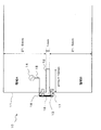
なお、本例において、アンテナ装置10はMIMOシステムの2GHz受信帯用(2110MHz〜2170MHz)にチューニングされているものとする。また、本例のアンテナ装置10あるいは後述するアンテナ装置10A〜10Dは、図1に示すように、携帯電話機などの移動無線端末(無線装置)1におけるアンテナ装置として用いられる。
この移動無線端末1は、アンテナ装置10(10A〜10D)と、アンテナ装置10(10A〜10D)が取り付けられる筐体30とを有している。アンテナ装置10(10A〜10D)は、後述するように、基板11を用いて構成される。この基板11上には、アンテナ装置10(10A〜10D)を用いて無線通信処理を行なう無線回路20がそなえられている。
In this example, it is assumed that the
The
図1及び図3に示すアンテナ装置10は、例示的に、スリット12を形成された矩形状の基板11と、給電部14と、給電線15と、アンテナエレメント16と、キャパシタ17と、インダクタ18とをそなえる。
スリット12は、基板11の一辺(短辺)の中央部分において、その一辺に直交する方向に切り込まれて直線状に形成される。本例において、このスリット12の切り込み長さ(開放端13から基板11内への侵入距離)dは10mm(約0.07λ)であり、ノッチアンテナにおいて必要とされるスリットの長さと比較すると極めて短くなっている。また、スリット12の幅は1mmとしている。
The
The
本例において、このスリット12は、図2に示すように、スリット12が形成された基板11の一辺の略半分の長さlaと、スリット12の内周長の半分の長さlb(ただし、lb=lx+ly)との合計値lが、およそλ/4つまり使用波長λの略4分の1になるように形成される。具体的に、図1及び図3に示すアンテナ装置10においては、l=21.5mm(=la)+10mm(=lx)+0.5mm(=ly)=32mmであるのに対し、2140MHzにおける波長λの4分の1の長さがおよそ35mmであることから、両者がほぼ等しいことがわかる。
In this example, as shown in FIG. 2, the
なお、lxはスリット12の切り込み長さ(侵入距離d)であり、lyはスリット12の幅の半分の長さである。また、アンテナ装置10において、長さlaは、基板11の一辺の半分の長さよりもスリット12の幅の半分の長さlyだけ短くなっており、厳密に基板11の一辺の半分の長さではない。つまり、長さlaは、上述したように、スリット12を形成された基板11の一辺の略半分の長さになっている。
In addition, lx is the cut length (penetration distance d) of the
ここで、図1に示すアンテナ装置10の構成を、図3を用いて詳細に説明する。
アンテナエレメント16は、整合回路を介してスリットの開放端13を跨ぐように基板11に配置され取り付けられる。本例では、整合回路の一例として、キャパシタ17及びインダクタ18を用いる。ここで、スリット12で分断された基板11の一方の側(給電部14を配置される側;図3中上側)を領域A、逆側を領域Bとする。
Here, the configuration of the
The
アンテナエレメント16の一端は、インダクタ18を介して領域Aの基板11に接続され、また、アンテナエレメント16の他端は、キャパシタ17を介して領域Bの基板11に接続される。なお、インダクタ18は、インピーダンス調整用であり、共振周波数には直接関係しない。また、本例では、キャパシタ17のキャパシタンスは0.5pF、インダクタ18のインダクタンスは1.5nHとするが、あくまで一例であり、本件はこれらの値に限定されるものではない。
One end of the
さらに、アンテナエレメント16の一端は、領域Aに設けられた給電線15を介して給電部14によって給電される。
ここで、図4及び図5を用いて、本アンテナの動作原理について説明する。
図4及び図5は、シミュレーションによって得られた、図1に示すアンテナ装置10の基板11における電流分布を示す。なお、電流分布の観測周波数は2140MHzである。
Furthermore, one end of the
Here, the operating principle of this antenna will be described with reference to FIGS.
4 and 5 show the current distribution in the
まず、アンテナ装置10は、スリット12の内周の長さによって変化するインダクタンスとキャパシタ17のキャパシタンスとにより共振する。この共振はループアンテナ型の共振であり、図4で示すように、スリット12の周囲の基板11上には渦電流が発生する(図4の符号19で示す矢印参照)。
さらに、この渦電流は、図5で示すように、基板11の領域A及び領域Bのそれぞれにほぼ同じ向きの電流を誘起する(図5の符号20で示す矢印参照)。
First, the
Furthermore, as shown in FIG. 5, this eddy current induces currents in substantially the same direction in each of the regions A and B of the substrate 11 (see the arrow indicated by
ここで、上述したように、基板11の一辺の略半分の長さと、スリット12の内周長の半分の長さとを合計するとおよそλ/4であることから、領域A及び領域Bにおける基板11は、それぞれλ/4の長さを有するアンテナ素子となる。このため、スリット12が形成された基板11の一辺は、全体としてλ/2の長さを有するダイポールアンテナのように動作する。
Here, as described above, the sum of the length of approximately half of one side of the
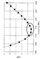
ここで、図6に、シミュレーションによって得られた、図1で示すアンテナ装置10のVSWR(Voltage Standing Wave Ratio)特性を示す。
この図6から、図1で示すアンテナ装置10は、目的周波数(2110MHz〜2170MHz)においてVSWRが3以下であり、良好な特性を示していることが分かる。
上述したように、一実施形態のアンテナ装置10によると、スリット12を形成された基板11の一辺がアンテナ素子として機能するので、一般的なノッチアンテナのスリットに比べて極めて短いスリットによって、極めて優れた特性を得ることができる。
Here, FIG. 6 shows VSWR (Voltage Standing Wave Ratio) characteristics of the
From FIG. 6, it can be seen that the
As described above, according to the
また、アンテナエレメント16を基板11の一辺の中央部分に配置するので、モノポールアンテナと設置領域が競合しない。
さらに、スリット12の長さつまり開放端13から基板11内への侵入距離dがノッチアンテナと比較して極めて短く、基板11上における配線の引き回しや部品の実装などの制約をほとんど受けない。
In addition, since the
Furthermore, the length of the
〔2〕第1変形例
図7は、本件のアンテナ装置の第1変形例の構成を示す図である。なお、図7中、既述の符号を付した各構成については、前述の各構成と同様の機能を具備するので、その詳細な説明は省略する。この図7に示すように、第1変形例のアンテナ装置10Aでは、図1で示した直線状のスリット12に代えて、所定の位置で図中上方に折り曲げたL字形のスリット12Aが形成されている。なお、本例におけるスリット12Aの内周長の半分の長さは10.5mmであり、上述した一実施形態におけるスリット12の内周長の半分の長さlbと等しい。
[2] First Modification FIG. 7 is a diagram showing a configuration of a first modification of the antenna device of the present case. In addition, in FIG. 7, since each structure which attached | subjected the code | symbol mentioned above has the function similar to each above-mentioned structure, the detailed description is abbreviate | omitted. As shown in FIG. 7, in the
図8は、シミュレーションによって得られた、図7で示すアンテナ装置10AのVSWR特性を示している。
この図8から、図7に示すL字形のスリット12Aを用いた場合でも、アンテナ装置10Aは、目的周波数(2110MHz〜2170MHz)においてVSWRが3以下であり、良好な特性を示していることが分かる。
FIG. 8 shows the VSWR characteristics of the
From FIG. 8, it can be seen that even when the L-shaped
従って、上述した第1変形例によれば、上述したアンテナ装置10と同様の作用効果が得られるほか、L字形のスリット12Aを用いることで、スリット12Aの内周長をスリット12の内周長と同等に保ったままで開放端13から基板11内への侵入距離dを短くすることができる。これにより、上述したアンテナ装置10と同等の良好な特性を得ながら、基板11上の配線や部品の実装の自由度を向上することができる。具体的に、アンテナ装置10ではd=10mmであるのに対し、アンテナ装置10Aでは、図7に示すように、d=7mmとなる。
Therefore, according to the first modified example described above, the same effects as the
〔3〕第2変形例
図9は、本件のアンテナ装置の第2変形例の構成を示す図である。なお、図9中、既述の符号を付した各構成については、前述の各構成と同様の機能を具備するので、その詳細な説明は省略する。この図9に示すように、第2変形例のアンテナ装置10Bでは、図1で示した直線状のスリット12に代えて、所定の位置で図中下方に折り曲げたL字形のスリット12Bが形成されている。なお、本例におけるスリット12Bの内周長の半分の長さは10.5mmであり、上述した一実施形態におけるスリット12の内周長の半分の長さlbと等しい。
[3] Second Modification FIG. 9 is a diagram showing a configuration of a second modification of the antenna device of the present case. In addition, in FIG. 9, since each structure to which the above-mentioned code | symbol was attached | subjected has the function similar to each above-mentioned structure, the detailed description is abbreviate | omitted. As shown in FIG. 9, in the
図10は、シミュレーションによって得られた、図9で示すアンテナ装置10BのVSWR特性を示す。
この図10から、図9に示すL字形のスリット12Bを用いた場合でも、アンテナ装置10Bは、目的周波数(2110MHz〜2170MHz)においてVSWRが3以下であり、良好な特性を示していることが分かる。
FIG. 10 shows the VSWR characteristics of the
From FIG. 10, it can be seen that even when the L-shaped
従って、上述した第2変形例によれば、上述したアンテナ装置10と同様の作用効果が得られるほか、第1変形例と同様、L字形のスリット12Bを用いることで、スリット12Bの内周長をスリット12の内周長と同等に保ったままで開放端13から基板11内への侵入距離dを短くすることができる。これにより、上述したアンテナ装置10と同等の良好な特性を得ながら、基板11上の配線や部品の実装の自由度を向上することができる。具体的に、アンテナ装置10ではd=10mmであるのに対し、アンテナ装置10Bでは、図9に示すように、d=7mmとなる。
Therefore, according to the second modified example described above, the same operational effects as those of the
〔4〕第3変形例
図11は、本件のアンテナ装置の第3変形例の構成を示す図である。なお、図11中、既述の符号を付した各構成については、前述の各構成と同様の機能を具備するので、その詳細な説明は省略する。この図11に示すように、第3変形例のアンテナ装置10Cでは、図1で示した直線状のスリット12に代えて、T字形のスリット12Cが形成されている。なお、本例におけるスリット12Cの内周長の半分の長さは10.7mmであり、上述した一実施形態におけるスリット12の内周長の半分の長さlbとほぼ等しい。
[4] Third Modification FIG. 11 is a diagram illustrating a configuration of a third modification of the antenna device of the present case. In addition, in FIG. 11, about each structure to which the above-mentioned code | symbol was attached | subjected, since the same function as each above-mentioned structure is provided, the detailed description is abbreviate | omitted. As shown in FIG. 11, in the
図12は、シミュレーションによって得られた、図11で示すアンテナ装置10CのVSWR特性を示す。
この図12から、図11に示すT字形のスリット12Cを用いた場合でも、アンテナ装置10Cは、目的周波数(2110MHz〜2170MHz)においてVSWRが3以下であり、良好な特性を示していることが分かる。
FIG. 12 shows the VSWR characteristics of the
From FIG. 12, it can be seen that even when the T-shaped
従って、上述した第3変形例によれば、上述したアンテナ装置10と同様の作用効果が得られるほか、第1変形例及び第2変形例と比較し、スリット12Cの内周長をスリット12の内周長と同等に保ったままで開放端13からの侵入距離dを更に短くすることができる。これにより、上述したアンテナ装置10と同等の良好な特性を得ながら、基板11上の配線や部品の実装の自由度を一層向上することができる。具体的に、アンテナ装置10ではd=10mmであるのに対し、アンテナ装置10Cでは、図11に示すように、d=6mmとなる。
Therefore, according to the above-described third modified example, the same operational effects as the above-described
〔5〕第4変形例
図13は、本件のアンテナ装置の第4変形例の構成を示す図である。なお、図13中、既述の符号を付した各構成については、前述の各構成と同様の機能を具備するので、その詳細な説明は省略する。この図13に示すように、第4変形例のアンテナ装置10Dでは、図1で示した直線状のスリット12の長さよりも短い直線状のスリット12Dが形成されている。具体的に、アンテナ装置10では、スリット12の切り込み長さlx=d=10mmであるのに対し、アンテナ装置10Dでは、スリット12Dの切り込み長さlx=d=6mmである。これにより、アンテナ装置10Dの動作周波数を、例えば、Bluetoothや無線LANなどで使用される周波数である2400MHz〜2480MHzにチューニングしている。
[5] Fourth Modified Example FIG. 13 is a diagram showing a configuration of a fourth modified example of the antenna device of the present case. In addition, in FIG. 13, since each structure which attached | subjected the code | symbol mentioned already has the function similar to each above-mentioned structure, the detailed description is abbreviate | omitted. As shown in FIG. 13, in the
図13に示すように、本例において、このスリット12Dは、スリット12Dを形成された基板11の一辺の略半分の長さ(21.5mm)と、スリット12Dの内周長の半分の長さ(6.5mm)との合計は28mmになるよう形成されており、2440MHzにおける波長の4分の1の長さ(およそ30.7mm)にほぼ等しい。
図14は、シミュレーションによって得られた、図13で示すアンテナ装置10DのVSWR特性を示す。
As shown in FIG. 13, in this example, the
FIG. 14 shows the VSWR characteristic of the
この図14から、図13に示すアンテナ装置10Dは、目的周波数(2400MHz〜2480MHz)においてVSWRが3以下であり、良好な特性を示していることが分かる。
このように、上述した第4変形例によれば、上述したアンテナ装置10と同様の作用効果が得られるほか、スリットの内周長を変更することで、アンテナ装置の動作周波数を容易に変更することができる。なお、本例では、スリット長つまりはスリットの内周長を短くすることで、アンテナ装置の動作周波数を高くしたが、逆にスリット長を長くすることで動作周波数を低くすることもできる。
From FIG. 14, it can be seen that the
As described above, according to the above-described fourth modification, the same operational effects as those of the
また、上述した第4変形例は、上記の他の変形例と組み合わせて実施することも可能である。つまり、アンテナ装置10Dにおいて、スリット12Dを直線状に代えてL字形やT字形に形成しても良い。
〔6〕その他
以上、本件の好ましい実施形態について詳述したが、本件は、かかる特定の実施形態に限定されるものではなく、本件の趣旨を逸脱しない範囲内において、種々の変形、変更して実施することができる。
Further, the above-described fourth modified example can be implemented in combination with the other modified examples described above. That is, in the
[6] Others Although the preferred embodiment of the present invention has been described in detail above, the present invention is not limited to the specific embodiment, and various modifications and changes can be made without departing from the spirit of the present invention. Can be implemented.
例えば、上述した実施形態では、基板に92mm×44mmのサイズのものを用いたが、基板の大きさを変えることで設定周波数を調整することもできる。
また、上述した実施形態では、整合回路であるインダクタ18として、1.5nHのインダクタを用いたが、これを短絡線によって代用することもできる。さらに、インダクタ18のインダクタンスを調整することで、VSWR特性の良好な帯域幅を調整することができる。
For example, in the above-described embodiment, a substrate having a size of 92 mm × 44 mm is used. However, the set frequency can be adjusted by changing the size of the substrate.
In the above-described embodiment, a 1.5 nH inductor is used as the
また、スリットにかかる寸法(切り込み長さ、幅)などは、上述した寸法に限定されるものではない。
さらに、上述した一実施形態及び各変形例では、スリットの形状に矩形状、L字形及びT字形のものを用いたが、例えば、ジグザグ状、曲線状及び円形状など、様々な形状のスリットを用いてもよい。
Moreover, the dimension (cut length, width) etc. concerning a slit are not limited to the dimension mentioned above.
Furthermore, in the above-described embodiment and each modification, rectangular, L-shaped, and T-shaped slits are used. For example, slits having various shapes such as a zigzag shape, a curved shape, and a circular shape are used. It may be used.
また、本件のアンテナ装置は、携帯電話機だけでなく、無線を用いて通信を行なう装置全般において広く適用することができる。 In addition, the antenna device of the present case can be widely applied not only to mobile phones but also to all devices that perform communication using radio.
1 移動無線端末(無線装置)
10,10A,10B,10C,10D アンテナ装置
11 基板
12,12A,12B,12C,12D スリット
13 開放端
14 給電部
15 給電線
16 アンテナエレメント
17 キャパシタ(整合回路)
18 インダクタ(整合回路)
20 無線回路
30 筐体
1 Mobile wireless terminal (wireless device)
10, 10A, 10B, 10C,
18 Inductor (matching circuit)
20
Claims (4)
前記アンテナ装置が取り付けられる筐体と、
を有し、
前記スリットは、前記基板の一辺の中央に形成され、
前記スリットの内周長の半分の長さと前記一辺の半分もしくは略半分の長さとの合計値が、使用波長の略4分の1であることを特徴とする、無線装置。 An antenna device comprising: a substrate having a slit; and an antenna element attached to the substrate so as to straddle the open end of the slit via a matching circuit, and fed from one end side;
A housing to which the antenna device is attached;
I have a,
The slit is formed at the center of one side of the substrate,
Sum of the inner peripheral length half the length and the length of the one side of the half or substantially half of the slit, characterized in 1 der Rukoto approximately a quarter of the wavelength used, the radio equipment.
整合回路を介し前記スリットの開放端を跨ぐように前記基板に取り付けられ、一端側から給電されるアンテナエレメントと、を有し、
前記スリットは、前記基板の一辺の中央に形成され、
前記スリットの内周長の半分の長さと前記一辺の半分もしくは略半分の長さとの合計値が、使用波長の略4分の1であることを特徴とする、アンテナ装置。 A substrate having a slit;
It mounted on said substrate so as to straddle the open end of the slit through a matching circuit, possess an antenna element to be powered from one end, and
The slit is formed at the center of one side of the substrate,
Sum of the inner peripheral length half the length and the length of the one side of the half or substantially half of the slit, characterized in 1 der Rukoto approximately a quarter of the wavelength used, the antenna device.
Priority Applications (2)
| Application Number | Priority Date | Filing Date | Title |
|---|---|---|---|
| JP2010252779A JP5644397B2 (en) | 2010-11-11 | 2010-11-11 | Wireless device and antenna device |
| US13/239,994 US9054426B2 (en) | 2010-11-11 | 2011-09-22 | Radio apparatus and antenna device |
Applications Claiming Priority (1)
| Application Number | Priority Date | Filing Date | Title |
|---|---|---|---|
| JP2010252779A JP5644397B2 (en) | 2010-11-11 | 2010-11-11 | Wireless device and antenna device |
Publications (2)
| Publication Number | Publication Date |
|---|---|
| JP2012105134A JP2012105134A (en) | 2012-05-31 |
| JP5644397B2 true JP5644397B2 (en) | 2014-12-24 |
Family
ID=46047283
Family Applications (1)
| Application Number | Title | Priority Date | Filing Date |
|---|---|---|---|
| JP2010252779A Expired - Fee Related JP5644397B2 (en) | 2010-11-11 | 2010-11-11 | Wireless device and antenna device |
Country Status (2)
| Country | Link |
|---|---|
| US (1) | US9054426B2 (en) |
| JP (1) | JP5644397B2 (en) |
Families Citing this family (5)
| Publication number | Priority date | Publication date | Assignee | Title |
|---|---|---|---|---|
| CN204403956U (en) * | 2015-02-15 | 2015-06-17 | 北京京东方茶谷电子有限公司 | A kind of backlight module and display unit |
| US10811780B2 (en) * | 2015-05-28 | 2020-10-20 | Huawei Technologies Co., Ltd. | Slot antenna and electronic device |
| EP3382798B1 (en) * | 2015-12-24 | 2020-09-02 | Huawei Technologies Co., Ltd. | Slot antenna and terminal |
| CN109313300B (en) * | 2016-04-07 | 2021-10-01 | 大日本印刷株式会社 | Protective film, optical film, laminate, polarizing plate, image display device, and manufacturing method of polarizing plate |
| WO2019169003A1 (en) * | 2018-02-27 | 2019-09-06 | Thin Film Electronics Asa | Printed and/or thin film integrated circuit with integrated antenna, and methods of making and using the same |
Family Cites Families (17)
| Publication number | Priority date | Publication date | Assignee | Title |
|---|---|---|---|---|
| JP2000196342A (en) * | 1998-12-28 | 2000-07-14 | Kojima Press Co Ltd | Antenna |
| JP2002135029A (en) * | 2000-10-25 | 2002-05-10 | Hitachi Ltd | Transponder of moving object identification device |
| US6424300B1 (en) * | 2000-10-27 | 2002-07-23 | Telefonaktiebolaget L.M. Ericsson | Notch antennas and wireless communicators incorporating same |
| JP3830358B2 (en) | 2001-03-23 | 2006-10-04 | 日立電線株式会社 | Flat antenna and electric device having the same |
| GB0206670D0 (en) * | 2002-03-21 | 2002-05-01 | Koninkl Philips Electronics Nv | Improvements in or relating to wireless terminals |
| JP2004032303A (en) | 2002-06-25 | 2004-01-29 | Sony Ericsson Mobilecommunications Japan Inc | Notch antenna and portable radio communication terminal |
| JP3844717B2 (en) | 2002-07-19 | 2006-11-15 | ソニー・エリクソン・モバイルコミュニケーションズ株式会社 | Antenna device and portable radio communication terminal |
| JP4150621B2 (en) * | 2002-09-20 | 2008-09-17 | 富士通株式会社 | Foldable portable radio and chassis of the radio |
| JP2005086531A (en) * | 2003-09-09 | 2005-03-31 | Sony Corp | Wireless communication unit |
| JP2006140735A (en) * | 2004-11-11 | 2006-06-01 | Toshiba Corp | Planar antenna |
| US7132991B1 (en) * | 2005-04-15 | 2006-11-07 | Tamkang University | Miniature planar notch antenna using microstrip feed line |
| JP2007201743A (en) * | 2006-01-26 | 2007-08-09 | Renesas Technology Corp | Id tag |
| WO2008084801A1 (en) * | 2007-01-11 | 2008-07-17 | Panasonic Corporation | Wide-band slot antenna |
| JP5086004B2 (en) * | 2007-08-30 | 2012-11-28 | 富士通株式会社 | Tag antenna and tag |
| US7916090B2 (en) * | 2007-09-04 | 2011-03-29 | Sierra Wireless, Inc. | Antenna configurations for compact device wireless communication |
| JP2010062976A (en) * | 2008-09-05 | 2010-03-18 | Sony Ericsson Mobile Communications Ab | Notch antenna and wireless device |
| JP5114357B2 (en) * | 2008-10-09 | 2013-01-09 | 株式会社日立製作所 | Wireless IC tag |
-
2010
- 2010-11-11 JP JP2010252779A patent/JP5644397B2/en not_active Expired - Fee Related
-
2011
- 2011-09-22 US US13/239,994 patent/US9054426B2/en not_active Expired - Fee Related
Also Published As
| Publication number | Publication date |
|---|---|
| JP2012105134A (en) | 2012-05-31 |
| US9054426B2 (en) | 2015-06-09 |
| US20120119963A1 (en) | 2012-05-17 |
Similar Documents
| Publication | Publication Date | Title |
|---|---|---|
| JP3658639B2 (en) | Surface mount type antenna and radio equipped with the antenna | |
| US11133605B2 (en) | Antenna structure | |
| JP4384102B2 (en) | Portable radio device and antenna device | |
| CN103117452B (en) | A kind of novel LTE terminal antenna | |
| JP5637565B2 (en) | Multiband antenna and mobile terminal | |
| US20100289709A1 (en) | Antenna and wireless communication device | |
| JP2012518300A (en) | Antenna configuration, printed circuit board, portable electronic device, and conversion kit | |
| CN103151601A (en) | Bottom edge slot coupled antenna | |
| JP2016514933A (en) | Multiband antenna | |
| WO2019086866A1 (en) | Hybrid closed slot lte antenna | |
| JP2005295493A (en) | Antenna device | |
| KR20150110291A (en) | Multiband hybrid antenna | |
| WO2006098089A1 (en) | Antenna assembly and radio communication apparatus employing same | |
| JP5644397B2 (en) | Wireless device and antenna device | |
| JP2011119949A (en) | Card device | |
| CN102017307A (en) | Portable radio equipment | |
| JP2019047183A (en) | antenna | |
| JP2010074489A (en) | Antenna device | |
| JP2006067234A (en) | Antenna device | |
| JP2012169805A (en) | Multiband antenna | |
| JP6825429B2 (en) | Multi-band antenna and wireless communication device | |
| JP5700122B2 (en) | ANTENNA DEVICE AND ELECTRONIC DEVICE | |
| JP2010130100A (en) | Multiband antenna apparatus | |
| US20150188223A1 (en) | Wireless communication device | |
| JP2014022782A (en) | Antenna circuit board and antenna device |
Legal Events
| Date | Code | Title | Description |
|---|---|---|---|
| A621 | Written request for application examination |
Free format text: JAPANESE INTERMEDIATE CODE: A621 Effective date: 20130805 |
|
| A977 | Report on retrieval |
Free format text: JAPANESE INTERMEDIATE CODE: A971007 Effective date: 20140219 |
|
| A131 | Notification of reasons for refusal |
Free format text: JAPANESE INTERMEDIATE CODE: A131 Effective date: 20140311 |
|
| A521 | Written amendment |
Free format text: JAPANESE INTERMEDIATE CODE: A523 Effective date: 20140428 |
|
| TRDD | Decision of grant or rejection written | ||
| A01 | Written decision to grant a patent or to grant a registration (utility model) |
Free format text: JAPANESE INTERMEDIATE CODE: A01 Effective date: 20141007 |
|
| A61 | First payment of annual fees (during grant procedure) |
Free format text: JAPANESE INTERMEDIATE CODE: A61 Effective date: 20141020 |
|
| R150 | Certificate of patent or registration of utility model |
Ref document number: 5644397 Country of ref document: JP Free format text: JAPANESE INTERMEDIATE CODE: R150 |
|
| LAPS | Cancellation because of no payment of annual fees |