JP5641237B2 - Noise addition circuit, noise addition method - Google Patents
Noise addition circuit, noise addition method Download PDFInfo
- Publication number
- JP5641237B2 JP5641237B2 JP2011075513A JP2011075513A JP5641237B2 JP 5641237 B2 JP5641237 B2 JP 5641237B2 JP 2011075513 A JP2011075513 A JP 2011075513A JP 2011075513 A JP2011075513 A JP 2011075513A JP 5641237 B2 JP5641237 B2 JP 5641237B2
- Authority
- JP
- Japan
- Prior art keywords
- pixel
- noise
- value
- determination value
- coefficient
- Prior art date
- Legal status (The legal status is an assumption and is not a legal conclusion. Google has not performed a legal analysis and makes no representation as to the accuracy of the status listed.)
- Expired - Fee Related
Links
Images


Landscapes
- Image Processing (AREA)
- Facsimile Image Signal Circuits (AREA)
Description
ノイズ付加回路、ノイズ付加方法に関する。 The present invention relates to a noise addition circuit and a noise addition method.
一般に、伝送路等により伝送される信号に混入するノイズは、ノイズフィルタ等により除去される。しかし、画像の場合、画像データの質感を高めるために、ノイズが付加される場合がある。 In general, noise mixed in a signal transmitted through a transmission path or the like is removed by a noise filter or the like. However, in the case of an image, noise may be added to improve the texture of the image data.
一般に、伝送路等により伝送される信号に混入するノイズは、ノイズフィルタ等により除去される。しかし、画像の場合、例えば階調数を少なくする等の処理後の画像データにおける不具合(例えば疑似輪郭)を解消して質感の低下を抑えるために、ノイズが付加される場合がある(例えば、特許文献1〜4参照)。
In general, noise mixed in a signal transmitted through a transmission path or the like is removed by a noise filter or the like. However, in the case of an image, for example, noise may be added in order to eliminate a defect (for example, pseudo contour) in the processed image data such as reducing the number of gradations and suppress deterioration in texture (for example, (See
ところで、画像への適切なノイズ付加は、人間にとっては質感の向上として認識される。このため、画像に応じた適切なノイズの付加が要求されている。 Incidentally, appropriate addition of noise to an image is perceived as an improvement in texture for humans. For this reason, it is required to add appropriate noise according to the image.
本発明の一観点によれば、着目画素を含む領域におけるエッジの有無を判定してエッジ判定値を出力するエッジ判定部と、前記着目画素を含む領域の平坦度を判定して平坦度判定値を出力する平坦度判定部と、前記エッジ判定値と前記平坦度判定値とを演算して係数を生成する係数生成部と、前記着目画素を含む領域の画素値と乱数に基づいて、前記着目画素にノイズを付加したノイズ付加画素を生成するノイズ付加処理部と、前記係数に基づいて、前記着目画素と前記ノイズ付加画素とを合成して合成画素を生成する画素合成部を含む。 According to an aspect of the present invention, an edge determination unit that determines the presence / absence of an edge in an area including a target pixel and outputs an edge determination value, and determines a flatness determination value by determining flatness of the area including the target pixel Based on a pixel value and a random number of a region including the target pixel, a coefficient generation unit that calculates the edge determination value and the flatness determination value, and generates a coefficient. A noise addition processing unit that generates a noise addition pixel in which noise is added to the pixel; and a pixel synthesis unit that generates a synthesis pixel by synthesizing the pixel of interest and the noise addition pixel based on the coefficient.
本発明の一観点によれば、画像に応じた適切なノイズを付加することが可能となる。 According to one aspect of the present invention, it is possible to add appropriate noise according to an image.
(第一実施形態)
以下、第一実施形態を図1及び図2に従って説明する。
図1に示すように、画像処理装置は例えばデジタルカメラ(DSC:Digital Still Camera)等の撮像装置に搭載され、図示しない撮像素子(例えばCCD(Charge Coupled Device)イメージセンサ)から出力される画像データGDを処理する。
(First embodiment)
Hereinafter, the first embodiment will be described with reference to FIGS. 1 and 2.
As shown in FIG. 1, the image processing apparatus is mounted on an imaging apparatus such as a digital camera (DSC: Digital Still Camera), for example, and image data output from an imaging element (for example, a CCD (Charge Coupled Device) image sensor) not shown. Process the GD.
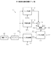
画像処理装置は、ノイズ付加回路10を含む。ノイズ付加回路10は、画像データGDに対して、ノイズを付加する。この画像データGDは、例えばRAWデータである。なお、撮像装置に依存する処理(例えば、ホワイトバランス等)後のデータでもよい。ノイズを付加する処理は、画像の質感や粒状感を向上するために行われる。また、この画像データGDは、YCbCr形式の信号のY(輝度)データとCb,Cr(色差)データである。なお、YCoCg形式(Y:輝度、Co,Cg:色差)、YUV形式、RGB形式などのデータでもよい。
The image processing apparatus includes a
画像データGDは、ノイズ付加回路10のラインメモリ11に供給される。ラインメモリ11は、複数ライン(例えば、3ライン)の画素データを記憶する容量に設定されている。ラインメモリ11のライン数は、ノイズ付加に関する処理において必要とする画素数に応じて設定されている。ノイズ付加回路10は、1つの画素を着目画素とし、その着目画素と周辺の複数の画素の画素データに基づいて、着目画素に対してノイズを付加するか否かを判定する。また、ノイズ付加回路10は、着目画素と周辺の複数の画素の画素データに基づいて、着目画素に対して付加するノイズの量(値)を算出する。
The image data GD is supplied to the
ラインメモリ11は、画像データGDの画素データを順次記憶する。そして、ラインメモリ11は、ブロック単位(例えば、3×3画素)の画素データBD(以下、単にブロックBDという場合がある)を出力する。ブロックのサイズは、ラインメモリ11が記憶するライン数に応じて設定されている。例えば、ラインメモリ11は、3×3画素のブロックで、画素データBDを出力する。ブロック単位の画素データBDは、エッジ判定部12、平坦度判定部13、ノイズ付加処理部14に供給される。上記したように、ブロックBDは、着目画素P0の画素データと、着目画素P0の周辺の画素の画素データを含む。この着目画素P0の画素データは、ピクセル合成部17に供給される。
The
なお、ラインメモリ11は、画像データGDとして供給される各画素の画素データを順次記憶し、演算に必要なブロックの画素データを記憶すると、そのブロックBDを出力する。そして、ラインメモリ11は、供給される画素データに応じてブロックの画像データを出力する。
The
例えば、画像データGDのサイズをm×n画素(m,nは正数)とする。画像データGDに含まれる各画素の画像データを、例えば、画像の左上を原点とし、水平方向(横方向)をx、垂直方向(縦方向)をyとし、画素G(x,y)で表す。従って、xは各ラインにおける画素の位置を示し、yはライン番号を示す。つまり、xとyは、画素の位置を示す座標値である。 For example, the size of the image data GD is m × n pixels (m and n are positive numbers). The image data of each pixel included in the image data GD is represented by, for example, a pixel G (x, y) where the upper left corner of the image is the origin, the horizontal direction (horizontal direction) is x, and the vertical direction (vertical direction) is y. . Therefore, x indicates the pixel position in each line, and y indicates the line number. That is, x and y are coordinate values indicating pixel positions.
ラインメモリ11には、先ず1ライン目の画像データ{画素G(1,1),G(2,1),・・・,G(m,1)}が記憶される。次に、2ライン目の画像データ{画素G(1,2),G(2,2),・・・,G(m,2)}が記憶される。そして、3ライン目の3つの画像データ{画素G(1,3),G(2,3),G(3,3)}が記憶されると、3×3画素のブロックが構成される。従って、ラインメモリ11は、9個の画素{G(1,1),G(2,1),G(3,1)G(1,2),G(2,2),G(3,2),G(1,3),G(2,3),G(3,3)}の画素データを、ブロックBDとして出力する。この時、着目画素P0は、ブロックの中央にある画素、つまり画素G(2,2)である。
The
次いで、4つ目の画素G(4,3)がラインメモリ11に記憶されると、9個の画素{G(2,1),G(3,1),G(4,1)G(2,2),G(3,2),G(4,2),G(2,3),G(3,3),G(4,3)}により1つのブロックが構成される。従って、ラインメモリ11は、このブロックBDを出力する。この時の着目画素P0は画素G(3,2)である。
Next, when the fourth pixel G (4,3) is stored in the
以下の説明において、画素データに基づいて各処理が実行される。つまり扱うデータは画素データ等である。しかし、画素のデータであるため、必要に応じて、単に画素を処理する(画素を演算する)として説明する。 In the following description, each process is executed based on the pixel data. That is, the data to be handled is pixel data or the like. However, since it is pixel data, it is assumed that the pixel is simply processed (the pixel is calculated) as necessary.
エッジ判定部12は、ブロックBDに基づいて、該ブロックBDにおけるエッジの有無を判定し、判定結果に応じたエッジ判定値REを出力する。例えば、エッジ判定部12は、ブロックBDを構成し、所定の方向(縦、横、斜め)に隣接する複数(本実施形態では3つ)の画素データの差分値を算出し、差分値と判定しきい値EDthとを比較する。この差分値が判定しきい値EDth以下の場合にエッジ有りと判定し、差分値が判定しきい値より大きい場合にエッジ無しと判定する。そして、エッジ判定部12は、ブロックBDにエッジが存在しない場合に値が[1]のエッジ判定値REを出力し、エッジが存在する場合に[0]のエッジ判定値REを出力する。
The
平坦度判定部13は、ブロックBDにおける平坦度(凹凸度)を判定し、その判定結果に応じた平坦度判定値RFを出力する。平坦度判定値RFは、0以上1以下の値をとる。例えば、平坦度判定部13は、平均偏差を算出する演算器を含む。平坦度判定部13には、外部レジスタ等から設定値SFLが供給される。設定値SFLは、ゲイン及びオフセットのうちの少なくとも1つを含む。平坦度判定部13は、演算器による演算結果(平均偏差値)に、設定値SFLを演算(乗算)して算出した値を平坦度判定値RFとして出力する。なお、また、平均偏差以外の方法によりブロックの平坦度を判定するようにしてもよい。
The
演算器15は、エッジ判定部12から出力されるエッジ判定値REに、平坦度判定部13から出力される平坦度判定値RFを乗算し、その乗算結果α0を出力する。
選択部16には、演算器15から算出値(係数)α0が供給され、外部レジスタ等から設定値(係数)α1及び選択信号SEが供給される。選択部16は、選択信号SEに応答して、算出値α0又は設定値α1を係数αとして出力する。演算器15と選択部16は、係数αを生成する係数生成部に含まれる。
The
The
ノイズ付加処理部14には、設定値Saが例えば外部レジスタから供給される。設定値Saは、後述する各種の設定値を含む。ノイズ付加処理部14は、設定値Saに基づいて、ブロックBDに含まれる着目画素P0にノイズを付加してノイズ付加画素P1を生成する。
The set value Sa is supplied to the noise
図1に示すように、ピクセル合成部17には、着目画素P0、ノイズ付加画素P1、及び係数αが供給される。ピクセル合成部17は、係数αに基づいて、着目画素P0とノイズ付加画素P1とを合成して合成画素P2を生成する。例えば、ピクセル合成部17は、着目画素P0とノイズ付加画素P1とを、係数αに基づいて、アルファブレンドして合成画素P2を生成する。具体的には、ピクセル合成部17は、着目画素P0、ノイズ付加画素P1、及び係数αに基づいて、以下の演算式、
P2=P0×(1−α)+P1×α
により合成画素P2を算出する。
As shown in FIG. 1, the
P2 = P0 × (1−α) + P1 × α
Thus, the composite pixel P2 is calculated.
係数αは、0以上1以下の値である。着目画素P0に乗算する値を第2の係数β(=1−α)とする。この第2の係数βは、第1の係数αの増加に従って減少する値となる。詳しくは、第2の係数βと第1の係数αとを互いに加算した結果が定数[1]となる値である。つまり、第2の係数βは、第1の係数αに対して反比例する。従って、上記式の第1項[P0×(1−α)]は、第2の係数βに対して比例、即ち第1の係数αに対して反比例する。そして、上記式の第2項[P1×α]は、第1の係数αに対して比例する。 The coefficient α is a value between 0 and 1. A value multiplied by the pixel of interest P0 is set as a second coefficient β (= 1−α). The second coefficient β is a value that decreases as the first coefficient α increases. Specifically, the value obtained by adding the second coefficient β and the first coefficient α to each other is a constant [1]. That is, the second coefficient β is inversely proportional to the first coefficient α. Accordingly, the first term [P0 × (1−α)] of the above equation is proportional to the second coefficient β, that is, inversely proportional to the first coefficient α. The second term [P1 × α] of the above equation is proportional to the first coefficient α.
上記したように、平坦度判定部13は、供給される9個の画素に基づいて平坦度判定値RFを算出する。従って、算出値α0は、ブロック毎に生成される。従って、算出値α0を選択した場合、画像データGDの画素値に応じて係数αが出力される。これにより、画像データGDに状態(画素値)に応じた比率で着目画素P0とノイズ付加画素P1が合成(ブレンド)された合成画素P2が生成される。
As described above, the
また、選択部16において、算出値α0が選択されたときの係数αは、平坦度判定部13により判定されたブロックBDの平坦度(凹凸度)を示す。従って、合成画素P2は、着目画素P0に対して、ノイズ付加画素P1を平坦度に応じて合成した値、つまり平坦度に応じたノイズ量を付加した画素となる。
In addition, the coefficient α when the
一方、設定値α1は、ブロックにかかわらず一定の値である。従って、設定値α1を選択した場合、一定値の係数αが出力される。これにより、画像データGDの全体に対して同じ比率で着目画素P0とノイズ付加画素P1が合成(ブレンド)された合成画素P2が生成される。 On the other hand, the set value α1 is a constant value regardless of the block. Therefore, when the set value α1 is selected, a constant value coefficient α is output. As a result, a combined pixel P2 is generated by combining (blending) the target pixel P0 and the noise-added pixel P1 with the same ratio with respect to the entire image data GD.
上記したように、算出値α0を選択したときの係数αは、エッジ判定部12から出力されるエッジ判定値REに、平坦度判定部13から出力される平坦度判定値RFを乗算した値である。エッジ判定部12は、ブロックにエッジが含まれる場合に[0]のエッジ判定値REを出力し、ブロックにエッジが含まれない場合に[1]のエッジ判定値REを出力する。従って、係数αは、ブロックにエッジが含まれる場合に[0]となり、エッジが含まれない場合に平坦度判定値RFと等しくなる。
As described above, the coefficient α when the calculated value α0 is selected is a value obtained by multiplying the edge determination value RE output from the
上記したように、ピクセル合成部17は、係数αが[0]のときに着目画素P0と等しい合成画素P2を生成する。つまり、エッジを含むブロックの着目画素P0には、ノイズが付加されないこととなる。一方、エッジを含まないブロックにおいて、凹凸があるブロック、即ちエッジではない凹凸を含まないブロックについて、係数αに応じて着目画素P0に対してノイズ付加画素P1を合成して合成画素P2を生成する。このように構成されたノイズ付加回路10は、局所的なノイズの付加を可能としている。例えば、砂浜や木目、ビルのレンガといった元々若干のザラつきがある画像領域では、係数αが0より大きいため、ブロックの着目画素P0にノイズを付加する。このような画像領域では、ノイズを付加することによって視覚的に好適なザラつき感を生じる。つまり、ノイズを付加した方が好ましい画像領域について、ノイズを付加することにより、より好ましい質感が得られるようにすることができる。
As described above, the
一方、係数αが0、即ちブロックに含まれる画素値の差が0または小さい(判定しきい値以下)の場合、ピクセル合成部17は、着目画素P0と等しい合成画素P2を生成する。平坦度が小さなブロック、つまり平坦度が小さな画像領域は、例えば光沢のある車のボディのような部分である。このような画像領域については、画素にノイズを付加すると、例えば光沢が無くなってしまい、被写体の質感が劣化する。つまり、ノイズの付加は好ましくない画像領域については、画素にノイズを付加しないことで、質感の劣化を抑制することができる。
On the other hand, when the coefficient α is 0, that is, the difference between the pixel values included in the block is 0 or small (below the determination threshold value), the
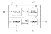
図2に示すように、ノイズ付加処理部14は、平滑化フィルタ21、偏差演算部22、疑似乱数生成部23、ノイズ画素生成部24を含む。
平滑化フィルタ21には、ブロックBDが供給される。平滑化フィルタ21は、ブロックBDの各画素を平滑化して生成した平滑画素Pmを生成する。例えば、平滑化フィルタ21は、ブロックBDに含まれる偶数個の画素値、例えばブロックBDに含まれる着目画素P0を除く8個の周辺画素の平均値を算出し、その平均値を平滑画素Pmとして出力する。この平滑画素Pmは、偏差演算部22とノイズ画素生成部24に供給される。なお、平滑化フィルタ21において、種々のフィルタ、例えばメディアンフィルタを用いることもできる。
As illustrated in FIG. 2, the noise
A block BD is supplied to the smoothing
偏差演算部22は、平滑化フィルタ21から出力される平滑画素Pmに基づいて、偏差値σを算出する。偏差値σは、平滑画素Pmからの移動量をクリップ(制限)する制限値である。例えば、偏差演算部22は、平滑画素Pmを引数とした一次式、
σ=A×Pm+B
により、偏差値σを算出する。なお、A,Bは設定値であり、例えば外部レジスタにより設定される。平滑画素Pmを引数とした一次式を用いるのは、実画像データについて、質感のよいノイズを付加した画素値を実験等により生成し、実画像データの画素値に対するノイズ量のゆらぎ(偏差)のプロットが、一次式とよくあうためである。また、一次式とすることにより、小さな回路規模の偏差演算部22により偏差値σを算出することができる、つまりノイズ付加処理部14の回路規模、ひいてはノイズ付加回路10の回路規模の増加を抑制することができる。
The
σ = A × Pm + B
Is used to calculate the deviation value σ. A and B are set values, and are set by an external register, for example. A linear expression using the smooth pixel Pm as an argument is used to generate a pixel value to which good-quality noise is added from actual image data by experiment or the like, and the fluctuation (deviation) of the noise amount with respect to the pixel value of the actual image data. This is because the plot matches the linear equation well. Further, by using the linear expression, the deviation value σ can be calculated by the
疑似乱数生成部23には、設定値Ssが供給される。疑似乱数生成部23は、設定値Ssを基準値として、乱数Rを生成する。疑似乱数生成部23は、回路規模と効果のトレードオフにより、混合合同法により乱数Rを発生するように構成されている。乱数Rは、ほぼ均等な確率で所定範囲内の値となる。この範囲は、上記偏差がとりうる値の最大値に応じて設定される。
A set value Ss is supplied to the
ノイズ画素生成部24は、上記の平滑画素Pm、偏差値σ、乱数Rに基づいて、ノイズ付加画素P1を生成する。例えば、ノイズ画素生成部24は、乱数Rを偏差値σに応じてクリップした補助値Rtを算出する。この補助値Rtの算出は、乱数Rに対する剰余演算により算出される。つまり、
Rt=R%(2σ+1)
但し、%は剰余演算、
により、補助値Rtを算出する。
The noise
Rt = R% (2σ + 1)
Where% is the remainder operation,
Thus, the auxiliary value Rt is calculated.
次に、ノイズ画素生成部24は、算出した補助値Rtを、平滑画素Pmに付加してノイズ付加画素P1を生成する。このとき、ノイズ画素生成部24は、平滑画素Pmを中心値として、偏差値σの範囲内の補助値Rtを付加する。つまり、ノイズ画素生成部24は、
P1=Pm+(Rt−σ)
により、ノイズ付加画素P1を算出する。
Next, the noise
P1 = Pm + (Rt−σ)
Thus, the noise added pixel P1 is calculated.
また、ノイズ画素生成部24には、設定値Soが例えば外部レジスタにより設定される。設定値Soは、算出した値のノイズ付加画素P1と、供給される着目画素P0と等しい値の画素P1を出力する割合を設定するものである。ノイズ画素生成部24は、乱数Rと設定値Soとを比較し、比較結果に応じて、算出値のノイズ付加画素P1又は着目画素P0と等しい画素P1を出力する。例えば、乱数Rが設定値So以上のときに算出値のノイズ付加画素P1を出力し、乱数Rが設定値So未満のときに着目画素P0と等しい画素P1を出力する。
In the noise
上記したように、乱数Rは、ほぼ均等な確率で所定の範囲の値をとる。これに対し、設定値Soが設定される。例えば乱数Rが取りうる値を[0]〜[15]とし、設定値Soを[8]とすると、1/2の確率で着目画素P0と等しい画素P1が出力される。また、設定値Soを[0]とすると、算出値のノイズ付加画素P1が毎回出力される。 As described above, the random number R takes a value in a predetermined range with a substantially equal probability. On the other hand, a set value So is set. For example, if the values that can be taken by the random number R are [0] to [15] and the set value So is [8], a pixel P1 that is equal to the pixel of interest P0 is output with a probability of 1/2. If the set value So is [0], the noise-added pixel P1 of the calculated value is output every time.
以上記述したように、本実施形態によれば、以下の効果を奏する。
(1)エッジ判定部12は、ブロックBD(ブロック単位の画素データBD)に基づいて、該ブロックBDにおけるエッジの有無を判定し、判定結果に応じたエッジ判定値REを出力する。平坦度判定部13は、ブロックBDにおける平坦度(凹凸度)を判定し、その判定結果に応じた平坦度判定値RFを出力する。演算器15は、エッジ判定値REに平坦度判定値RFを乗算する。その乗算結果(算出値α0)に応じた係数αがピクセル合成部17に供給される。ピクセル合成部17は、係数αに基づいて、着目画素P0とノイズ付加画素P1とを合成して合成画素P2を生成する。
As described above, according to the present embodiment, the following effects can be obtained.
(1) The
ブロックBDにエッジが含まれる場合、[0]のエッジ判定値REが出力されるため、係数αは[0]となる。従って、エッジが含まれるブロックBDでは、着目画素P0と等しい値の合成画素P2が出力される。また、平坦度が小さなブロックBDでは、[0]又は[0]に近い値の平坦度判定値RFが出力されるため、係数αは[0]となる。従って、画素値の凹凸が小さい領域では、着目画素P0と等しい値の合成画素P2が出力される。このように、画像の領域の状態に応じた合成画素P2、つまり画像に応じた適切なノイズを付加することができる。 When an edge is included in the block BD, since the edge determination value RE of [0] is output, the coefficient α is [0]. Therefore, in the block BD including the edge, the composite pixel P2 having the same value as the target pixel P0 is output. In addition, in the block BD having a small flatness, the flatness determination value RF having a value close to [0] or [0] is output, so the coefficient α is [0]. Accordingly, in a region where the unevenness of the pixel value is small, a composite pixel P2 having a value equal to the target pixel P0 is output. In this way, it is possible to add the composite pixel P2 corresponding to the state of the image area, that is, appropriate noise corresponding to the image.
(2)ノイズ付加処理部14の平滑化フィルタ21は、ブロックBDの画素値を平滑化した平滑画素Pmを出力する。偏差演算部22は、平滑画素Pmの偏差値σを算出する。そして、ノイズ画素生成部24は、偏差値σに対応するノイズ(補助値Rt)を平滑画素Pmに付加してノイズ付加画素P1を生成する。従って、ブロックBDの画素に応じた量のノイズ(補助値Rt)を付加することができる。
(2) The smoothing
(3)ノイズ付加処理部14は疑似乱数生成部23を含み、その疑似乱数生成部23にて生成した乱数Rに基づいてノイズ付加画素P1を生成する。従って、ランダムな量のノイズを付加することができる。
(3) The noise
(4)ノイズ付加回路10は選択部16を含み、算出値α0と設定値α1とを選択信号SEに基づいて選択し、選択した値を係数αとしてピクセル合成部17に供給するようにした。従って、画像に応じて部分的にノイズを付加するモードと、画像全体にノイズを付加するモードとを切り替えることができる。そして、設定値α1を適宜変更することにより、好適なノイズを付加することができる。
(4) The
(第二実施形態)
以下、第二実施形態を図4に従って説明する。
なお、第一実施形態と同じ構成については同じ符号を付してその説明の全て又は一部を省略する。
(Second embodiment)
Hereinafter, a second embodiment will be described with reference to FIG.
In addition, about the same structure as 1st embodiment, the same code | symbol is attached | subjected and all or one part of the description is abbreviate | omitted.
図4に示すように、ノイズ付加回路40のラインメモリ11は、供給される画像データGDのうち、複数ライン(例えば、3ライン)の画素データを記憶し、ブロック単位(例えば、3×3画素)の画素データBD(ブロックBD)を出力する。ブロックBDは、着目画素P0の画素データと、着目画素P0の周辺の画素の画素データを含む。ブロックBDは、エッジ判定部12、平坦度判定部13、ノイズ付加処理部14、輝彩度判定部41に供給される。着目画素P0の画素データは、ピクセル合成部17に供給される。
As shown in FIG. 4, the
輝彩度判定部41には、外部レジスタ等から、設定値SYCが供給される。設定値SYCは、輝度と彩度とを合成する比率を指定する値であり、0以上1以下の範囲の値である。輝彩度判定部41は、ブロックBDにおける輝彩度RBを算出する。ブロックBDに含まれる各画素データの値は、YCbCr形式のデータである。輝度RYは、Yデータの値であり、例えば、ブロックBDに含まれる複数画素の値の平均値である。なお、Yデータを、ブロックBDに含まれる着目画素の値としてもよい。輝彩度判定部41は、2つの色差Cb,Crから彩度RCを、例えば、
RC=(|Cb|+|Cr|)/2
のように、2つの色差の絶対値の平均値として求める。なお、色差データCb,Crは、ブロックBDに含まれる画素に対応するデータである。
The set value SYC is supplied to the brightness /
RC = (| Cb | + | Cr |) / 2
As described above, the average value of the absolute values of the two color differences is obtained. The color difference data Cb and Cr are data corresponding to the pixels included in the block BD.
そして、輝彩度判定部41は、輝度RYと彩度RCとに基づいて、輝彩度RBを、例えば、
RB=RY×(1−SYC)+RC×SYC
により求める。この演算は、αブレンドと呼ばれ、設定値SYCはブレンド比である。このように算出された輝彩度RBは、輝度・彩度が低いほど0に近い値を取る。設定値SYCを変更する、つまり輝度RYと彩度RCとの割合を変更することは、輝度RYのみの参照、彩度RCのみの参照によるノイズ付加の抑制を可能とする。
Then, the luminance
RB = RY × (1-SYC) + RC × SYC
Ask for. This calculation is called α blend, and the set value SYC is a blend ratio. The brightness saturation RB calculated in this way takes a value closer to 0 as the luminance / saturation is lower. Changing the set value SYC, that is, changing the ratio between the luminance RY and the saturation RC, makes it possible to suppress noise addition by referring to only the luminance RY and referring only to the saturation RC.
合成部42は、平坦度判定部13から出力される平坦度判定値RFと、輝彩度判定部41から出力される輝彩度RBとを合成して、合成判定値CRを生成する。例えば、合成部42は、
CR=(RF+RB)/2
のように、平坦度判定値RFと輝彩度RBとの平均値を合成判定値CRとする。
The combining
CR = (RF + RB) / 2
As described above, the average value of the flatness determination value RF and the luminance saturation RB is set as the combined determination value CR.
演算器15は、エッジ判定部12から出力されるエッジ判定値REに、合成部42から出力される合成判定値CRを乗算し、その乗算結果(係数α0)を出力する。
選択部16は、選択信号SEに応答して、演算器15から出力される係数α0と、外部レジスタ等から供給される係数α1とのうちの何れか一方を選択し、その選択した係数と等しい係数αを出力する。
The
In response to the selection signal SE, the
ピクセル合成部17は、係数αに基づいて、着目画素P0とノイズ付加画素P1とを合成して合成画素P2を生成する。
次に、ノイズ付加回路40の作用を説明する。
The
Next, the operation of the
ピクセル合成部17から出力される合成画素P2は、係数αに比例したノイズを含む。係数αは、ブロックBDの平坦度(凹凸度)と輝彩度を示す。例えば、ポートレートの黒髪や風景写真の影の部分のように輝度の低い画像領域、人間の肌のように彩度が低い画像領域に対応する輝彩度RBは[0]に近い値となる。輝彩度RBが一般的に、輝度・彩度が低い画像領域のノイズは、人間が不快と感じやすい。従って、ノイズ付加回路40は、輝彩度RBが[0]または[0]に近い画像領域に対するノイズの付加を抑制する。
The synthesized pixel P2 output from the
以上記述したように、本実施形態によれば、上記第一実施形態の効果に加え、以下の効果を奏する。
(5)輝彩度判定部41は、ブロックBDに基づいて、ブロックBDにおける輝度・彩度を判定し、判定結果に応じた輝彩度RBを出力する。合成部42は、平坦度判定部13から出力される平坦度判定値RFと輝彩度RBとを合成し、合成判定値CRを出力する。演算器15は、エッジ判定値REに合成判定値CRを乗算し、係数α0を生成する。ピクセル合成部17は、係数α(係数α0)に基づいて、着目画素P0とノイズ付加画素P1とを合成して合成画素P2を生成する。従って、ポートレートの黒髪や風景写真の影の部分等の輝度の低い画像領域や、人間の肌等の彩度が低い画像領域のように、人間が不快と感じやすい画像領域に対するノイズの付加を抑制することができる。
As described above, according to this embodiment, in addition to the effects of the first embodiment, the following effects can be obtained.
(5) The brightness /
(6)輝彩度判定部41は、ブロックBDのYCbCr信号に基づいて、輝度信号Yの輝度値RYと、色差信号Cb,Crの値の絶対値の平均値である彩度値RCを算出し、輝彩度RBを算出するようにした。このように輝彩度RBの算出をハードウェアにて実装する場合、ハードウェアにおける負荷が少なく、実装が容易である。
(6) The luminance
尚、上記各実施形態は、以下の態様で実施してもよい。
・上記各形態において、疑似乱数生成部23の構成を適宜変更しても良い。例えば、乗算合同法、平方採中法、線形合同法、等の方法により乱数Rを生成するようにしてもよい。
In addition, you may implement each said embodiment in the following aspects.
-In each said form, you may change suitably the structure of the pseudorandom
・上記各形態において、ノイズ付加処理部14の構成を適宜変更してもよい。
例えば、図3に示すようにノイズ付加処理部14を構成しても良い。このノイズ付加処理部14は、平滑化フィルタ21、偏差演算部22、ノイズデータ取得メモリコントローラ(以下、データ取得部)25、ノイズ画素生成部24を含む。
-In each said form, you may change the structure of the noise
For example, the noise
データ取得部25は、外部メモリ31に記憶されたデータを取得する。外部メモリ31に格納されたデータは、処理する画像データと同じデータサイズのノイズデータである。ノイズデータは、例えば、入射光を遮断した状態の撮像素子から出力される画像データである。なお、データ取得部25を、メモリ31を含む構成としてもよい。
The
この場合、データ取得部25から出力されるデータをRdとすると、ノイズ画素生成部24は、
Rt=(Rd−Doff)×σ×Dg
により補助値Rtを算出する。なお、Doffはオフセット、Dgはゲインであり、外部レジスタ等により設定される。
In this case, if the data output from the
Rt = (Rd−Doff) × σ × Dg
To calculate the auxiliary value Rt. Doff is an offset and Dg is a gain, which is set by an external register or the like.
そして、ノイズ画素生成部24は、算出した補助値Rtを偏差値σによりクリッピングした補助値Rt2(−σ≦Rt2≦σ)を算出する。そして、この補助値Rt2を平滑画素Pmに加算してノイズ付加画素P1(=Pm+Rt2)を生成する。
Then, the noise
また、外部メモリ31に格納するノイズデータとして、例えば、デジタル信号処理装置(DSP:Digital Signal Processor)などの処理装置により生成された乱数データとしてもよい。
The noise data stored in the
・ノイズを付加する対象画素に対して、その対象画素と周囲の8画素の画素値とに基づいて、エッジ判定等の各種の判定処理を行うようにしたが、複数の判定処理のうちの少なくとも1つについて、判定に用いる周囲の画素数を変更してもよい。例えば、平坦度判定部において、対象画素と周囲の24画素の画素値とに基づいて判定を行うようにしてもよい。なお、対象画像の周辺において、24画素の画素値が得られない場合には、5×5画素の範囲に含まれる周辺画素の画素値、例えば対象画素に隣接する8画素と範囲に含まれる11画素の合計20画素の画素値を用いて判定を行うようにしてもよい。 -Various determination processes such as edge determination are performed on the target pixel to which noise is added based on the target pixel and the pixel values of the surrounding eight pixels. At least of the plurality of determination processes For one, the number of surrounding pixels used for determination may be changed. For example, the flatness determination unit may perform the determination based on the target pixel and pixel values of surrounding 24 pixels. If a pixel value of 24 pixels cannot be obtained around the target image, pixel values of peripheral pixels included in the 5 × 5 pixel range, for example, 8 pixels adjacent to the target pixel and 11 included in the range You may make it perform determination using the pixel value of a total of 20 pixels.
・上記各形態では、偏差演算部22が一次式により偏差値σを算出するようにしたが、その他の方法により偏差値σを算出するようにしてもよい。例えば、区間毎の一次式(折れ線)により偏差値σを算出するようにしてもよい。また、テーブル(LUT:Look Up Table )を用いて偏差値σを得るようにしてもよい。これらの方法によると、偏差値σを実プロットとよりよく一致させることができる。
In each of the above embodiments, the
・上記各形態では、各種の設定値を例えば外部レジスタから設定することとしたが、設定方法を適宜変更してもよい。例えば、設定値を必要な処理部に予め設定する。また、画像処理装置を制御する制御部(例えばCPU)により設定してもよい。 In the above embodiments, various setting values are set from an external register, for example, but the setting method may be changed as appropriate. For example, a set value is preset in a necessary processing unit. Further, it may be set by a control unit (for example, CPU) that controls the image processing apparatus.
・上記各形態において、選択部16を省略してもよい。
また、選択部16に平坦度判定値RFと設定値α1とを供給し、選択信号SEにより選択した値を演算器15に供給する構成としてもよい。
In each of the above forms, the
Alternatively, the flatness determination value RF and the set value α1 may be supplied to the
・上記各形態において、ノイズを付加した着目画素P0の座標値を記憶し、その座標値に対して水平方向又は垂直方向の少なくとも一方に連続する画素に対してノイズを付加するようにノイズ付加処理部又はピクセル合成部を構成しても良い。連続してノイズを付加する方向と連続数は、例えば外部レジスタにより設定される。このような構成により、ノイズ粒子の密度や、ノイズ粒子の大きさを制御することが可能となる。 In each of the above embodiments, the noise addition process is performed so that the coordinate value of the pixel of interest P0 to which noise is added is stored, and noise is added to pixels that are continuous in at least one of the horizontal direction and the vertical direction with respect to the coordinate value. Or a pixel synthesis unit. The direction and the number of continuous additions of noise are set by an external register, for example. With such a configuration, the density of noise particles and the size of noise particles can be controlled.
・図5に示すように、ノイズ付加回路50を構成してもよい。このノイズ付加回路50は、輝度判定部51と、彩度判定部52と、合成部53とを含む。輝度判定部51は、ブロックBDのYCbCr信号に基づいて輝度値RYを出力する。彩度判定部52は、ブロックBDのYCbCr信号に基づいて彩度値RC(=(|Cb|+|Cr|)/2)を出力する。合成部53は、平坦度判定部13から出力される平坦度判定値RFと、輝度判定部51から出力される輝度値RYと、彩度判定部52から出力される彩度値RCを合成して合成判定値CRを生成する。このようにしても、上記第二実施形態と同様の効果を得ることができる。
As shown in FIG. 5, a
・図4に示す合成部42は、平均以外の方法、例えばαブレンドにより合成判定値CRを生成するようにしてもよい。
上記各実施形態に関し、以下の付記を開示する。
(付記1)
着目画素を含む領域におけるエッジの有無を判定してエッジ判定値を出力するエッジ判定部と、
前記着目画素を含む領域の平坦度を判定して平坦度判定値を出力する平坦度判定部と、
前記エッジ判定値と前記平坦度判定値とを演算して係数を生成する係数生成部と、
前記着目画素を含む領域の画素値に基づいて、前記着目画素にノイズを付加したノイズ付加画素を生成するノイズ付加処理部と、
前記係数に基づいて、前記着目画素と前記ノイズ付加画素とを合成して合成画素を生成する画素合成部と、
を含むことを特徴とするノイズ付加回路。
(付記2)
前記係数生成部は、前記エッジ判定値に前記平坦度判定値を乗算する演算器を含み、その演算器の出力結果に応じて前記係数を生成する、ことを特徴とする請求項1に記載のノイズ付加回路。
(付記3)
前記着目画素を含む領域における輝度と彩度とに基づく判定値を出力する輝彩度判定部と、
前記平坦度判定値と前記輝彩度判定部の判定値とを合成して合成判定値を出力する合成部と、
を含み、
前記係数生成部は、前記エッジ判定値と前記合成判定値とを演算して前記係数を生成する、
ことを特徴とする請求項1に記載のノイズ付加回路。
(付記4)
前記輝彩度判定部は、前記着目画素を含む領域における輝度データの輝度値と、前記着目画素を含む領域における2つの色差データに基づいて算出した彩度値と、に基づいて前記判定値を算出する、ことを特徴とする請求項3に記載のノイズ付加回路。
(付記5)
前記輝彩度判定部は、設定値に応じた比率で前記輝度値と前記彩度値とを合成して前記判定値を算出する、ことを特徴とする請求項4に記載のノイズ付加回路。
(付記6)
前記係数生成部は、前記エッジ判定値に前記合成判定値を乗算する演算器を含み、その演算器の出力結果に応じて前記係数を生成する、ことを特徴とする請求項3〜5のうちの何れか一項に記載のノイズ付加回路。
(付記7)
前記係数生成部は、前記演算器の算出値と設定値とが入力され、選択信号に応じて前記算出値と前記設定値の何れか一方を前記係数として出力する選択部を含むことを特徴とする付記2又は6に記載のノイズ付加回路。
(付記8)
前記ノイズ付加処理部は、
前記着目画素を含む前記領域の画素を平滑化して平滑画素を生成する平滑化フィルタと、
前記平滑画素の偏差を算出する偏差演算部と、
乱数を生成する乱数生成部と、
前記偏差に応じた前記乱数を前記平滑画素に付加して前記ノイズ付加画素を生成するノイズ画素生成部と
を含むことを特徴とする付記1〜7のうちの何れか一項に記載のノイズ付加回路。
(付記9)
前記ノイズ付加処理部は、
前記着目画素を含む前記領域の画素を平滑化して平滑画素を生成する平滑化フィルタと、
前記平滑画素の偏差を算出する偏差演算部と、
メモリに記憶されたデータを読み出して出力するデータ取得部と、
前記偏差に応じた前記データを前記平滑画素に付加して前記ノイズ付加画素を生成するノイズ画素生成部と
を含むことを特徴とする付記1〜7のうちの何れか一項に記載のノイズ付加回路。
(付記10)
前記ノイズ画素生成部は、前記乱数又は前記データと設定値とを比較し、比較結果に応じて前記着目画素と等しい画素又は前記ノイズ付加画素を出力する、ことを特徴とする付記8又は9に記載のノイズ付加回路。
(付記11)
前記画素合成部は、
前記係数に基づいて、前記着目画素と前記ノイズ付加画素とをアルファブレンドして前記合成画素を生成する、ことを特徴とする付記1〜10のうちの何れか一項に記載のノイズ付加回路。
(付記12)
着目画素を含む領域におけるエッジの有無を判定してエッジ判定値を生成し、
前記着目画素を含む領域の平坦度を判定して平坦度判定値を生成し、
前記エッジ判定値と前記平坦度判定値とを演算して係数を生成し、
前記着目画素を含む領域の画素値に基づいて、前記着目画素にノイズを付加したノイズ付加画素を生成し、
前記係数に基づいて、前記着目画素と前記ノイズ付加画素とを合成して合成画素を生成する、
ことを特徴とするノイズ付加方法。
(付記13)
前記着目画素を含む領域における輝度と彩度とに基づく判定値を生成し、
前記輝度と前記彩度とに基づく判定値と前記平坦度判定値とを合成して合成判定値を生成し、
前記エッジ判定値と前記合成判定値とを演算して前記係数を生成する、
ことを特徴とする付記12に記載のノイズ付加方法。
The
The following notes are disclosed regarding the above embodiments.
(Appendix 1)
An edge determination unit that determines the presence or absence of an edge in the region including the target pixel and outputs an edge determination value;
A flatness determination unit that determines flatness of a region including the target pixel and outputs a flatness determination value;
A coefficient generation unit that calculates the edge determination value and the flatness determination value to generate a coefficient;
A noise addition processing unit that generates a noise-added pixel obtained by adding noise to the pixel of interest based on a pixel value of a region including the pixel of interest;
A pixel combining unit that generates a combined pixel by combining the target pixel and the noise-added pixel based on the coefficient;
A noise adding circuit comprising:
(Appendix 2)
The coefficient generation unit includes an arithmetic unit that multiplies the edge determination value by the flatness determination value, and generates the coefficient according to an output result of the arithmetic unit. Noise addition circuit.
(Appendix 3)
A brightness / saturation determination unit that outputs a determination value based on luminance and saturation in a region including the target pixel;
A combining unit that combines the flatness determination value and the determination value of the brightness saturation determination unit and outputs a combined determination value;
Including
The coefficient generation unit calculates the edge determination value and the combination determination value to generate the coefficient,
The noise adding circuit according to
(Appendix 4)
The luminance saturation determination unit calculates the determination value based on a luminance value of luminance data in an area including the target pixel and a saturation value calculated based on two color difference data in the area including the target pixel. The noise adding circuit according to claim 3, wherein the noise adding circuit is calculated.
(Appendix 5)
The noise addition circuit according to claim 4, wherein the brightness saturation determination unit calculates the determination value by combining the luminance value and the saturation value at a ratio according to a set value.
(Appendix 6)
The coefficient generation unit includes an arithmetic unit that multiplies the edge determination value by the composite determination value, and generates the coefficient according to an output result of the arithmetic unit. The noise adding circuit according to any one of the above.
(Appendix 7)
The coefficient generation unit includes a selection unit that receives the calculated value and the set value of the arithmetic unit and outputs either the calculated value or the set value as the coefficient in response to a selection signal. The noise adding circuit according to appendix 2 or 6,
(Appendix 8)
The noise addition processing unit
A smoothing filter that smoothes the pixels in the region including the target pixel to generate smooth pixels;
A deviation calculator for calculating a deviation of the smooth pixel;
A random number generator for generating random numbers;
The noise addition according to any one of
(Appendix 9)
The noise addition processing unit
A smoothing filter that smoothes the pixels in the region including the target pixel to generate smooth pixels;
A deviation calculator for calculating a deviation of the smooth pixel;
A data acquisition unit that reads and outputs data stored in the memory;
The noise addition according to any one of
(Appendix 10)
Additional Note 8 or 9, wherein the noise pixel generation unit compares the random number or the data with a set value, and outputs a pixel equal to the pixel of interest or the noise added pixel according to a comparison result. The noise adding circuit described.
(Appendix 11)
The pixel composition unit
11. The noise addition circuit according to
(Appendix 12)
Determine the presence or absence of an edge in the area containing the pixel of interest and generate an edge determination value,
The flatness determination value is generated by determining the flatness of the region including the target pixel,
A coefficient is generated by calculating the edge determination value and the flatness determination value,
Based on the pixel value of the region including the target pixel, a noise added pixel in which noise is added to the target pixel is generated,
Based on the coefficient, the pixel of interest and the noise-added pixel are combined to generate a combined pixel.
A noise adding method characterized by the above.
(Appendix 13)
Generating a determination value based on luminance and saturation in a region including the target pixel;
A composite determination value is generated by combining the determination value based on the luminance and the saturation and the flatness determination value,
Calculating the edge determination value and the combined determination value to generate the coefficient;
The noise adding method according to
11 ラインメモリ
12 エッジ判定部
13 平坦度判定部
14 ノイズ付加処理部
17 ピクセル合成部(画素合成部)
41 輝彩度判定部
42 合成部
P0 着目画素
P1 ノイズ付加画素
P2 合成画素
RE エッジ判定値
RF 平坦度判定値
RB 輝彩度
CR 合成判定値
α 係数
DESCRIPTION OF
41
Claims (8)
前記着目画素を含む領域の平坦度を判定して平坦度判定値を出力する平坦度判定部と、
前記エッジ判定値と前記平坦度判定値とを演算して係数を生成する係数生成部と、
前記着目画素を含む領域の画素値と乱数に基づいて、前記着目画素にノイズを付加したノイズ付加画素を生成するノイズ付加処理部と、
前記係数に基づいて、前記着目画素と前記ノイズ付加画素とを合成して合成画素を生成する画素合成部と、
を含むことを特徴とするノイズ付加回路。 An edge determination unit that determines the presence or absence of an edge in the region including the target pixel and outputs an edge determination value;
A flatness determination unit that determines flatness of a region including the target pixel and outputs a flatness determination value;
A coefficient generation unit that calculates the edge determination value and the flatness determination value to generate a coefficient;
A noise addition processing unit that generates a noise-added pixel in which noise is added to the target pixel, based on a pixel value of a region including the target pixel and a random number ;
A pixel combining unit that generates a combined pixel by combining the target pixel and the noise-added pixel based on the coefficient;
A noise adding circuit comprising:
前記平坦度判定値と前記輝彩度判定部の判定値とを合成して合成判定値を出力する合成部と、
を含み、
前記係数生成部は、前記エッジ判定値と前記合成判定値とを演算して前記係数を生成する、
ことを特徴とする請求項1に記載のノイズ付加回路。 A brightness / saturation determination unit that outputs a determination value based on luminance and saturation in a region including the target pixel;
A combining unit that combines the flatness determination value and the determination value of the brightness saturation determination unit and outputs a combined determination value;
Including
The coefficient generation unit calculates the edge determination value and the combination determination value to generate the coefficient,
The noise adding circuit according to claim 1.
前記着目画素を含む領域の平坦度を判定して平坦度判定値を生成し、
前記エッジ判定値と前記平坦度判定値とを演算して係数を生成し、
前記着目画素を含む領域の画素値と乱数に基づいて、前記着目画素にノイズを付加したノイズ付加画素を生成し、
前記係数に基づいて、前記着目画素と前記ノイズ付加画素とを合成して合成画素を生成する、
ことを特徴とするノイズ付加方法。 Determine the presence or absence of an edge in the area containing the pixel of interest and generate an edge determination value,
The flatness determination value is generated by determining the flatness of the region including the target pixel,
A coefficient is generated by calculating the edge determination value and the flatness determination value,
Based on a pixel value and a random number in a region including the target pixel, a noise added pixel in which noise is added to the target pixel is generated,
Based on the coefficient, the pixel of interest and the noise-added pixel are combined to generate a combined pixel.
A noise adding method characterized by the above.
前記輝度と前記彩度とに基づく判定値と前記平坦度判定値とを合成して合成判定値を生成し、
前記エッジ判定値と前記合成判定値とを演算して前記係数を生成する、
ことを特徴とする請求項7に記載のノイズ付加方法。 Generating a determination value based on luminance and saturation in a region including the target pixel;
A composite determination value is generated by combining the determination value based on the luminance and the saturation and the flatness determination value,
Calculating the edge determination value and the combined determination value to generate the coefficient;
The noise adding method according to claim 7, wherein:
Priority Applications (1)
| Application Number | Priority Date | Filing Date | Title |
|---|---|---|---|
| JP2011075513A JP5641237B2 (en) | 2010-06-17 | 2011-03-30 | Noise addition circuit, noise addition method |
Applications Claiming Priority (3)
| Application Number | Priority Date | Filing Date | Title |
|---|---|---|---|
| JP2010138292 | 2010-06-17 | ||
| JP2010138292 | 2010-06-17 | ||
| JP2011075513A JP5641237B2 (en) | 2010-06-17 | 2011-03-30 | Noise addition circuit, noise addition method |
Publications (2)
| Publication Number | Publication Date |
|---|---|
| JP2012023708A JP2012023708A (en) | 2012-02-02 |
| JP5641237B2 true JP5641237B2 (en) | 2014-12-17 |
Family
ID=45777541
Family Applications (1)
| Application Number | Title | Priority Date | Filing Date |
|---|---|---|---|
| JP2011075513A Expired - Fee Related JP5641237B2 (en) | 2010-06-17 | 2011-03-30 | Noise addition circuit, noise addition method |
Country Status (1)
| Country | Link |
|---|---|
| JP (1) | JP5641237B2 (en) |
Families Citing this family (1)
| Publication number | Priority date | Publication date | Assignee | Title |
|---|---|---|---|---|
| CN110114799B (en) | 2017-01-10 | 2023-06-23 | 富士胶片株式会社 | Noise processing device and noise processing method |
Family Cites Families (4)
| Publication number | Priority date | Publication date | Assignee | Title |
|---|---|---|---|---|
| JPH08163594A (en) * | 1994-12-12 | 1996-06-21 | Sony Corp | Moving picture decoding method and moving picture decoding apparatus |
| JPH10155087A (en) * | 1996-11-20 | 1998-06-09 | Ricoh Co Ltd | Image processor |
| JP2007028348A (en) * | 2005-07-20 | 2007-02-01 | Noritsu Koki Co Ltd | Image processing apparatus and image processing method |
| JP2008109369A (en) * | 2006-10-25 | 2008-05-08 | Olympus Imaging Corp | Imaging apparatus and image processing method |
-
2011
- 2011-03-30 JP JP2011075513A patent/JP5641237B2/en not_active Expired - Fee Related
Also Published As
| Publication number | Publication date |
|---|---|
| JP2012023708A (en) | 2012-02-02 |
Similar Documents
| Publication | Publication Date | Title |
|---|---|---|
| KR101247646B1 (en) | Image combining apparatus, image combining method and recording medium | |
| US8107123B2 (en) | Tone correction apparatus, mobile terminal, image capturing apparatus, mobile phone, tone correction method and program for improve local contrast in bright and dark regions | |
| CN103685850B (en) | Image processing method and image processing apparatus | |
| JP5392560B2 (en) | Image processing apparatus and image processing method | |
| JP4810473B2 (en) | Image processing apparatus and image processing program | |
| JP2010244360A (en) | Image processing apparatus, image processing method, and computer program | |
| JP2013162359A (en) | Image processing apparatus and image processing method | |
| JP2005130484A (en) | Gradation correction apparatus and gradation correction program | |
| JP5641237B2 (en) | Noise addition circuit, noise addition method | |
| JP2011015277A (en) | Image processing device, image processing method, image processing program, and recording medium recording image processing program | |
| JP2001014454A (en) | Picture processor | |
| JP2013106151A (en) | Image processing apparatus and image processing method | |
| US20090046166A1 (en) | Image processing apparatus, image processing program, image processing method, and electronic camera for correcting texture of image | |
| JP2013207427A (en) | Image pickup device and image pickup method | |
| US11032446B2 (en) | Image processing device, image processing method, and program for correcting color in an image | |
| JP2008072604A (en) | Image processing system, device, media, program | |
| KR102003777B1 (en) | Apparatus and method for processing image | |
| JP2004112473A (en) | Gradation correction device | |
| JP2012010227A (en) | Image processing apparatus, and image processing method | |
| JP2007288484A (en) | Gradation correction processing device | |
| JP2021087083A (en) | Image processing device, image processing method, and program | |
| CN110035267B (en) | Image enhancement circuit and method | |
| WO2018034287A1 (en) | Information processing apparatus and program | |
| JP2007306083A (en) | Imaging apparatus and signal processing apparatus | |
| JP2011199787A (en) | Image processing apparatus and image processing method |
Legal Events
| Date | Code | Title | Description |
|---|---|---|---|
| A621 | Written request for application examination |
Free format text: JAPANESE INTERMEDIATE CODE: A621 Effective date: 20131129 |
|
| A131 | Notification of reasons for refusal |
Free format text: JAPANESE INTERMEDIATE CODE: A131 Effective date: 20140715 |
|
| A521 | Written amendment |
Free format text: JAPANESE INTERMEDIATE CODE: A523 Effective date: 20140908 |
|
| TRDD | Decision of grant or rejection written | ||
| A01 | Written decision to grant a patent or to grant a registration (utility model) |
Free format text: JAPANESE INTERMEDIATE CODE: A01 Effective date: 20141001 |
|
| A61 | First payment of annual fees (during grant procedure) |
Free format text: JAPANESE INTERMEDIATE CODE: A61 Effective date: 20141014 |
|
| R150 | Certificate of patent or registration of utility model |
Ref document number: 5641237 Country of ref document: JP Free format text: JAPANESE INTERMEDIATE CODE: R150 |
|
| S111 | Request for change of ownership or part of ownership |
Free format text: JAPANESE INTERMEDIATE CODE: R313111 |
|
| R350 | Written notification of registration of transfer |
Free format text: JAPANESE INTERMEDIATE CODE: R350 |
|
| LAPS | Cancellation because of no payment of annual fees |