JP5634793B2 - Display including waveguide, microprism and micromechanical light modulator - Google Patents
Display including waveguide, microprism and micromechanical light modulator Download PDFInfo
- Publication number
- JP5634793B2 JP5634793B2 JP2010180901A JP2010180901A JP5634793B2 JP 5634793 B2 JP5634793 B2 JP 5634793B2 JP 2010180901 A JP2010180901 A JP 2010180901A JP 2010180901 A JP2010180901 A JP 2010180901A JP 5634793 B2 JP5634793 B2 JP 5634793B2
- Authority
- JP
- Japan
- Prior art keywords
- light
- layer
- refractive index
- display
- optical waveguide
- Prior art date
- Legal status (The legal status is an assumption and is not a legal conclusion. Google has not performed a legal analysis and makes no representation as to the accuracy of the status listed.)
- Active
Links
Images


Classifications
-
- G—PHYSICS
- G02—OPTICS
- G02B—OPTICAL ELEMENTS, SYSTEMS OR APPARATUS
- G02B5/00—Optical elements other than lenses
- G02B5/04—Prisms
- G02B5/045—Prism arrays
-
- G—PHYSICS
- G02—OPTICS
- G02B—OPTICAL ELEMENTS, SYSTEMS OR APPARATUS
- G02B26/00—Optical devices or arrangements for the control of light using movable or deformable optical elements
- G02B26/08—Optical devices or arrangements for the control of light using movable or deformable optical elements for controlling the direction of light
- G02B26/0816—Optical devices or arrangements for the control of light using movable or deformable optical elements for controlling the direction of light by means of one or more reflecting elements
- G02B26/0833—Optical devices or arrangements for the control of light using movable or deformable optical elements for controlling the direction of light by means of one or more reflecting elements the reflecting element being a micromechanical device, e.g. a MEMS mirror, DMD
- G02B26/0841—Optical devices or arrangements for the control of light using movable or deformable optical elements for controlling the direction of light by means of one or more reflecting elements the reflecting element being a micromechanical device, e.g. a MEMS mirror, DMD the reflecting element being moved or deformed by electrostatic means
-
- G—PHYSICS
- G02—OPTICS
- G02B—OPTICAL ELEMENTS, SYSTEMS OR APPARATUS
- G02B6/00—Light guides; Structural details of arrangements comprising light guides and other optical elements, e.g. couplings
- G02B6/0001—Light guides; Structural details of arrangements comprising light guides and other optical elements, e.g. couplings specially adapted for lighting devices or systems
- G02B6/0011—Light guides; Structural details of arrangements comprising light guides and other optical elements, e.g. couplings specially adapted for lighting devices or systems the light guides being planar or of plate-like form
- G02B6/0033—Means for improving the coupling-out of light from the light guide
- G02B6/0035—Means for improving the coupling-out of light from the light guide provided on the surface of the light guide or in the bulk of it
- G02B6/0036—2-D arrangement of prisms, protrusions, indentations or roughened surfaces
-
- G—PHYSICS
- G02—OPTICS
- G02B—OPTICAL ELEMENTS, SYSTEMS OR APPARATUS
- G02B6/00—Light guides; Structural details of arrangements comprising light guides and other optical elements, e.g. couplings
- G02B6/0001—Light guides; Structural details of arrangements comprising light guides and other optical elements, e.g. couplings specially adapted for lighting devices or systems
- G02B6/0011—Light guides; Structural details of arrangements comprising light guides and other optical elements, e.g. couplings specially adapted for lighting devices or systems the light guides being planar or of plate-like form
- G02B6/0033—Means for improving the coupling-out of light from the light guide
- G02B6/0035—Means for improving the coupling-out of light from the light guide provided on the surface of the light guide or in the bulk of it
- G02B6/0038—Linear indentations or grooves, e.g. arc-shaped grooves or meandering grooves, extending over the full length or width of the light guide
-
- G—PHYSICS
- G02—OPTICS
- G02B—OPTICAL ELEMENTS, SYSTEMS OR APPARATUS
- G02B6/00—Light guides; Structural details of arrangements comprising light guides and other optical elements, e.g. couplings
- G02B6/0001—Light guides; Structural details of arrangements comprising light guides and other optical elements, e.g. couplings specially adapted for lighting devices or systems
- G02B6/0011—Light guides; Structural details of arrangements comprising light guides and other optical elements, e.g. couplings specially adapted for lighting devices or systems the light guides being planar or of plate-like form
- G02B6/0033—Means for improving the coupling-out of light from the light guide
- G02B6/0035—Means for improving the coupling-out of light from the light guide provided on the surface of the light guide or in the bulk of it
- G02B6/0045—Means for improving the coupling-out of light from the light guide provided on the surface of the light guide or in the bulk of it by shaping at least a portion of the light guide
- G02B6/0046—Tapered light guide, e.g. wedge-shaped light guide
-
- G—PHYSICS
- G09—EDUCATION; CRYPTOGRAPHY; DISPLAY; ADVERTISING; SEALS
- G09G—ARRANGEMENTS OR CIRCUITS FOR CONTROL OF INDICATING DEVICES USING STATIC MEANS TO PRESENT VARIABLE INFORMATION
- G09G3/00—Control arrangements or circuits, of interest only in connection with visual indicators other than cathode-ray tubes
- G09G3/20—Control arrangements or circuits, of interest only in connection with visual indicators other than cathode-ray tubes for presentation of an assembly of a number of characters, e.g. a page, by composing the assembly by combination of individual elements arranged in a matrix no fixed position being assigned to or needed to be assigned to the individual characters or partial characters
- G09G3/34—Control arrangements or circuits, of interest only in connection with visual indicators other than cathode-ray tubes for presentation of an assembly of a number of characters, e.g. a page, by composing the assembly by combination of individual elements arranged in a matrix no fixed position being assigned to or needed to be assigned to the individual characters or partial characters by control of light from an independent source
- G09G3/3433—Control arrangements or circuits, of interest only in connection with visual indicators other than cathode-ray tubes for presentation of an assembly of a number of characters, e.g. a page, by composing the assembly by combination of individual elements arranged in a matrix no fixed position being assigned to or needed to be assigned to the individual characters or partial characters by control of light from an independent source using light modulating elements actuated by an electric field and being other than liquid crystal devices and electrochromic devices
- G09G3/3473—Control arrangements or circuits, of interest only in connection with visual indicators other than cathode-ray tubes for presentation of an assembly of a number of characters, e.g. a page, by composing the assembly by combination of individual elements arranged in a matrix no fixed position being assigned to or needed to be assigned to the individual characters or partial characters by control of light from an independent source using light modulating elements actuated by an electric field and being other than liquid crystal devices and electrochromic devices based on light coupled out of a light guide, e.g. due to scattering, by contracting the light guide with external means
Description
(相互関連出願の参照)
2007年12月19日に出願された米国特許出願公開第12/004115号明細書、2009年8月13日に出願された米国特許出願公開第12/583156号明細書、2010年5月28日に出願された米国特許出願公開第12/802037号明細書、2008年12月18日に出願された国際公開第2008/087471号パンフレットが、参考文献として本明細書に包含されている。
(Refer to related applications)
US Patent Application Publication No. 12/004115 filed on December 19, 2007, US Patent Application Publication No. 12/583156 filed on August 13, 2009, May 28, 2010 US Patent Application Publication No. 12/802037, filed December 18, 2008, and WO 2008/087471 filed on Dec. 18, 2008 are incorporated herein by reference.
(技術分野)
本発明は一般にディスプレイに関する。より詳細には、本発明は、光導波路、光源および複数の電気機械画素を備えたディスプレイに関する。
(Technical field)
The present invention relates generally to displays. More particularly, the present invention relates to a display comprising a light guide, a light source and a plurality of electromechanical pixels.
現在、液晶ディスプレイは、フラットパネルディスプレイ市場を支配している。従来技術による液晶ディスプレイは、通常、照明のためのバックライトアセンブリ、光偏光子、カラーフィルタおよび中性密度フィルタ、ならびに薄膜トランジスタバックプレーンを備えた能動マトリックス液晶層を備えている。従来技術による典型的な液晶ディスプレイ(LCD)の総合光効率は、主として、バックライトアセンブリからの光を偏光子、カラーフィルタおよび中性密度フィルタのいくつかの層を通過させなければならないため、10%未満である。LCDが抱えている他の問題は、液晶の応答時間が遅く、そのために動画像を表示する際に好ましくない可視動アーチファクトが生じることである。 Currently, liquid crystal displays dominate the flat panel display market. Prior art liquid crystal displays typically comprise a backlight assembly for illumination, an optical polarizer, color filters and neutral density filters, and an active matrix liquid crystal layer with a thin film transistor backplane. The overall light efficiency of a typical liquid crystal display (LCD) according to the prior art is mainly because the light from the backlight assembly must pass through several layers of polarizers, color filters and neutral density filters. %. Another problem with LCDs is that the response time of liquid crystals is slow, which causes undesirable visual motion artifacts when displaying moving images.
最近、LCDに対する有効な代替として、光導波路に基づく微小機械フラットパネルディスプレイが提案された。これらのディスプレイは、典型的には、電気的に駆動される微小機械画素のマトリックスがその上に構築される平行な表面を備えたプレーナ型導波路からなっている。光源からの光は、導波路の1つまたは複数の側面から導波路に導入され、内部全反射によって導波路内に拘束される。光は、エバネッセント波に結合させることによって、あるいはプレーナ型導波路の表面を変形させることによって導波路の平らな表面から抽出され、それにより画像が生成される。画像を表示するために画素を同時に活性化させる際の固有の光漏話問題が存在している。1つの画素の状態によって他の画素の輝度が変化する。光漏話問題に対する解決法の1つは、画素を連続的に活性化させることである。そのためには極めて高速の微小機械アクチュエータが必要であるが、光効率が著しく低下することになる。カラー画像またはグレースケール画像を表示することは、一般的には実際的ではない。もう1つの共通の問題は、光の方向を観察者に向けて変えるためにミラー表面を使用することに関連している。同じミラー表面によって周辺光が反射して観察者に向かって戻るため、周辺光のレベルが高い場合、コントラストが著しく低下する。 Recently, micromechanical flat panel displays based on optical waveguides have been proposed as an effective alternative to LCDs. These displays typically consist of planar waveguides with parallel surfaces on which a matrix of electrically driven micromechanical pixels is built. Light from the light source is introduced into the waveguide from one or more sides of the waveguide and is constrained within the waveguide by total internal reflection. Light is extracted from the planar surface of the waveguide by coupling it to evanescent waves or by deforming the surface of the planar waveguide, thereby producing an image. There is an inherent light crosstalk problem when simultaneously activating pixels to display an image. The brightness of other pixels changes depending on the state of one pixel. One solution to the light crosstalk problem is to activate the pixels continuously. For this purpose, an extremely high-speed micromechanical actuator is required, but the light efficiency is significantly reduced. Displaying a color or grayscale image is generally not practical. Another common problem is associated with using a mirror surface to redirect the light toward the viewer. Since the ambient light is reflected by the same mirror surface and returns toward the viewer, the contrast is significantly reduced when the ambient light level is high.
本発明の第1の目的は、光導波路をベースとする従来技術によるディスプレイに典型的に見られる光漏話問題を効果的に解決するディスプレイを提供することである。本発明の第2の目的は、高いレベルの周辺光で動作するハイコントラスト文字ディスプレイを提供することである。 It is a first object of the present invention to provide a display that effectively solves the light crosstalk problem typically found in prior art displays based on optical waveguides. A second object of the present invention is to provide a high contrast character display that operates with a high level of ambient light.
本発明の一形態では、第1の目的は、光源と、光導波路とを備えたディスプレイを提供することによって達成される。光導波路は、複数の光出口に光を分散させる。個々の光出口で、画素は、光を観察者または光吸収体に選択的に導くことによって光を変調する。 In one form of the invention, the first object is achieved by providing a display comprising a light source and an optical waveguide. The optical waveguide disperses light at a plurality of light outlets. At each light outlet, the pixel modulates the light by selectively directing the light to an observer or light absorber.
本発明の実施形態によれば、第2の目的は、観察表面の大部分が光吸収コーティングで被覆されたディスプレイを提供することによって達成される。 According to an embodiment of the present invention, the second object is achieved by providing a display in which the majority of the viewing surface is coated with a light absorbing coating.
本発明の第2の目的は、光効率、画像品質およびコストの点でLCDと比肩し得るディスプレイを提供することである。光が内部全反射によって光路の大部分を移動するディスプレイを提供することによって高い光効率が達成され、また、高度に反射性のマイクロミラーからの反射がより少なくてすむようにすることによって光が変調される。高速で有効な光変調器を提供することによって、改善された画像品質が達成される。 A second object of the present invention is to provide a display that is comparable to LCDs in terms of light efficiency, image quality and cost. High light efficiency is achieved by providing a display in which light travels most of the light path by total internal reflection, and light is modulated by making less reflection from highly reflective micromirrors Is done. By providing a fast and effective light modulator, improved image quality is achieved.
本発明の第1の目的ならびに第2の目的は、添付の図面に示され、かつ以降の本明細書に記載されている新規なディスプレイによって達成される。 The first and second objects of the present invention are achieved by the novel display shown in the accompanying drawings and described hereinafter.
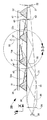
図面、とりわけ図1および2を参照すると、本発明のディスプレイの一形成が一括して数表示20で示されている。図1に最も良好に示されているように、ディスプレイ20には、ここでは、概ね長方形の形をした、断面が実質的にくさび形である光導波路21が含まれている。導波路21は、好ましいことには、値が約1.45と約1.6の間である屈折率n1を有するアクリル材料または他の光学的に透明な材料から構築されており、かつ、平行な側表面28および29によって結合された平行な第1および第2の末端表面26および27を備えている(図1参照)。また、導波路21には、主上部表面30および上部表面30と共に収斂する下部表面31が含まれている。図1に概略的に示されている下部表面31は、平らな表面であり、上部表面30との間に、値が約0.1度と約2.0度の間である角度22を形成している(図2)。また、下部表面31は、導波路21の上部表面30との間に可変角度を形成する湾曲した表面であってもよく、あるいは表示光の一様性を制御するための複数の階段状ファセットを含むことも可能である。上部表面30には複数の実質的に等しく間隔を隔てたマイクロプリズム32が構築されており、図1に概略的に示されているように側表面28と29の間に延在している。マイクロプリズム32は、リソグラフィを使用して、値が約1.45と約1.6の間である屈折率n2を有するUV硬化ポリマーから成形し、あるいは構築することができる。LED光源25は、導波路21の幅の広い方の縁26の近傍に設置されており、また、複数の傾斜マイクロミラー33は、マイクロプリズム32どうしの間に構築されている。図2には、1列の傾斜マイクロミラーが33a、33bおよび33cで示されている。また、図1には、カバーアセンブリ34の断面が示されている。カバーアセンブリ34のより詳細な構造が図3に示されている。
Referring to the drawings, and in particular to FIGS. 1 and 2, one formation of the display of the present invention is shown collectively as
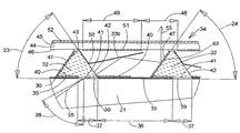
次に図面の図3を参照すると、多層オプティカルコーティングがより詳細に示されている。第1の層は、金属または多層誘電材料を使用して導波路21の上部表面30に構築された光反射層35である。光反射層35は、複数の光反射領域36および光透過領域37が形成されるようにパターン化されている。第2の光学層は、値が約1.3と約1.4の間である屈折率n3を有するフッ素樹脂または他の実質的に透明な材料から形成された光透過層39である。光透過層39は、図3に示されているように、導波路21の上部表面30の光透過領域37にのみ形成されている。また、光透過層39は、光反射層35と導波路21の上部表面30の間に形成された連続層であってもよい。第3の光学層は、光反射層35の上に形成された光吸収層40であり、この光吸収層40は、光反射層35を部分的に覆うようにパターン化されている。光反射層35の上部表面には、光吸収層40の代わりにブラックオキサイド層を形成することも可能である。
Referring now to FIG. 3 of the drawings, the multilayer optical coating is shown in more detail. The first layer is a
図3にはさらにマイクロプリズム32が示されている。個々のマイクロプリズム32は、光透過層39を介して導波路21の上部表面30に光結合された光入射ファセット41、および導波路21の上部表面30に対して傾斜し、導波路21の上部表面30との間に、値が約45度と約65度の間である角度23を形成している光射出ファセット42を備えている。マイクロプリズム32の第3のファセット43の上には反射ミラー膜が堆積し、光反射ファセット47を形成している。この光反射ファセット47は、同じく導波路21の上部表面30に対して傾斜しており、導波路21の上部表面30との間に、値が約30度と約50度の間である角度24を形成している。
FIG. 3 further shows a
また、図3には、本発明のこの形態のマイクロミラーの各々の構造を代表している複数の傾斜マイクロミラー33bのうちの1つが示されている。マイクロミラー33bは、薄いアルミニウム合金弾性膜を備えており、この薄いアルミニウム合金弾性膜は、マイクロプリズム32の光射出ファセット42の上部部分に貼り付けられており、導波路21の上部表面30に対して実質的に平行の軸50の周りで2つの方向に傾斜している。
FIG. 3 shows one of a plurality of tilted
図3には、さらに、マイクロプリズム32の上部ファセットに貼り付けられたカバーアセンブリ34が示されている。カバーアセンブリ34は、ガラスまたは他の実質的に透明な材料でできた基板44を備えている。基板44の下部表面46には、導電性光吸収膜でできた、あるいは導体層を含む多層膜でできた光吸収層51が構築されている。光吸収層51は、マイクロミラー33の真上に配置された複数の光吸収領域49および表示光射出領域48が形成されるようにパターン化されている。カバーアセンブリ34には、さらに、基板44の上部表面45に形成された光整形拡散板52が含まれている。
Also shown in FIG. 3 is a
周辺光を吸収するために、マイクロミラー33の上部表面にブラックオキサイド層を形成することができ、また、パターン化された光吸収層51を透明な導体に置き換えることができる。そのようにすることにより、パターン化された光吸収層51とマイクロミラー33を整列させる要求事項が除去される。
In order to absorb the ambient light, a black oxide layer can be formed on the upper surface of the
本発明のこの形態では、傾斜マイクロミラー33は静電引力によって動作している。導電性光反射層35および導電性光吸収層51は、傾斜マイクロミラー33のための固定電極として作用している。
In this form of the invention, the tilting
導電性光反射層35とマイクロミラー33の間に適切な電圧が印加されると、マイクロミラーは、静電引力によって下に向かって傾斜する。導電性光吸収層51とマイクロミラー33の間に適切な電圧が印加されると、マイクロミラーは、静電引力によって上に向かって傾斜する。
When an appropriate voltage is applied between the conductive
マイクロミラーのスティクションを防止するためには、マイクロミラーの縁とランディング表面の間に微小ギャップ58(図2)が必要である。この微小ギャップ58は、ランディング表面に微小スペーサを構築するか、あるいはマイクロミラーの縁全体がランディング表面に接触しないよう、マイクロミラーの微小部分を縁に沿って延在させることによって実現することができる。 In order to prevent micromirror stiction, a small gap 58 (FIG. 2) is required between the edge of the micromirror and the landing surface. This microgap 58 can be realized by building a microspacer on the landing surface, or by extending a micropart of the micromirror along the edge so that the entire micromirror edge does not contact the landing surface. .
図面の図2に最も良好に示されているように、導波路21の幅の広い方の縁26から入射した光線55は、内部全反射によって上部表面30および下部表面31で反射し、上部表面30に対する法線に向かって角度が変化する。光線55は、入射角が導波路21の屈折率n1および光透過層39の屈折率n3によって画定される臨界角38未満になると、光透過領域37を通って導波路21から射出する(図3)。光透過層39を通過した光線は、光入射ファセット41からマイクロプリズム32に入射し、マイクロプリズムの屈折率n2によって画定される角度が変化する。光線は、光射出ファセット42を通ってマイクロプリズムから射出する。
As best shown in FIG. 2 of the drawings, the
光線は、傾斜マイクロミラーの位置に応じて吸収され、あるいは観察者に向かって導かれる。傾斜マイクロミラーがマイクロミラー33b(図2)のようにアップ位置に位置している場合、マイクロプリズム32の光射出ファセット42から射出した光線の大部分は、マイクロミラーの下部表面で反射し、光反射ファセット47で反射して観察者に向かって導かれる。マイクロミラーがマイクロミラー33aおよび33cのように下に向かって傾斜すると、マイクロプリズム32の光射出ファセット42から射出した光線の大部分は、マイクロミラーの下部表面で反射し、光吸収層40で吸収される。
The light beam is absorbed depending on the position of the tilting micromirror or guided toward the observer. When the tilted micromirror is located at the up position as in the
マイクロミラーがダウン位置に傾斜している場合に、ギャップ58からの光の漏れを防止するために、ディスプレイ20は、光線がマイクロプリズム32の光射出ファセット42から射出することができる、導波路21の上部表面30に対する最小角度を制限している。この最小角度は、屈折率n1、n2、n3および角度23によって画定される。
To prevent light leakage from the gap 58 when the micromirror is tilted to the down position, the
次に図面の図4を参照すると、本発明のディスプレイの他の実施形態の横断面図が数表示70で一括して示されている。この最後の実施形態は、いくつかの点で図面の図1および2に示されている実施形態に類似しており、同様のコンポーネントを識別するために図4には同様の番号が使用されている。
Referring now to FIG. 4 of the drawings, a cross-sectional view of another embodiment of the display of the present invention is shown collectively with a
ディスプレイ70はフルカラーディスプレイであり、個々の画素が、赤、緑および青のサブピクセルからなっており、また、白色光源から、あるいは導波路21内で混合されるRGB光源からRGBカラーを分離するための二色性フィルタが個々の画素に含まれている。
The
ディスプレイ70には、光導波路21および導波路21の幅の広い方の縁26の近傍に設置されたLED光源25が含まれている。また、ディスプレイ70には、値が約1.45と約1.6の間である屈折率n4を有するガラスなどの実質的に透明な材料から構築された基板72が含まれている。基板72の下部表面74は、値が約1.3と約1.4の間である屈折率n3を有する実質的に透明な材料から形成された光学層71を介して導波路21の上部表面30に光結合されている。
The
複数の等しく間隔を隔てたマイクロプリズム32は、基板72の上部表面73に構築されており、また、傾斜マイクロミラー33は、マイクロプリズム32どうしの間に構築されている。この場合も、カバーアセンブリ34は、マイクロプリズム32の上部ファセットに貼り付けられている。
A plurality of equally spaced
次に図面の図5を参照すると、多層オプティカルコーティングがより詳細に示されている。第1の光学層は、基板72の上部表面73に形成された二色性フィルタ75である。第2の光学層は、二色性フィルタ75の上に構築された金属製の光反射層35である。光反射層35は、複数の光反射領域36および光透過領域37が形成されるようにパターン化されている。第3の光学層は、光反射層35の上に形成された光吸収層40であり、この光吸収層40は、光反射層35を部分的に覆うようにパターン化されている。
Referring now to FIG. 5 of the drawings, the multilayer optical coating is shown in more detail. The first optical layer is a
また、図5にはマイクロプリズム32が示されている。個々のマイクロプリズム32は、二色性フィルタ75を介して導波路21の上部表面30に光結合された光入射ファセット41、基板72および光学層71を備えている。また、個々のマイクロプリズム32には光射出ファセット42が含まれており、また、マイクロプリズム32の第3のファセット43の上にはミラー膜が堆積し、光反射ファセット47を形成している。
FIG. 5 shows a
また、図5には、図3に関連して上で説明した複数のマイクロミラー33のうちの1つおよびカバーアセンブリ34が示されている。
Also shown in FIG. 5 is one of the plurality of
図面の図4に最も良好に示されているように、導波路21の幅の広い方の縁26から入射した光線55は、内部全反射によって上部表面30および下部表面31で反射し、上部表面30に対する法線に向かって角度が変化する。光線55は、入射角が導波路21の屈折率n1および光透過層71の屈折率n3によって画定される臨界角38未満になると、上部表面30を通って導波路21から射出し、かつ、光透過層71を通って基板72に入射する(図5)。二色性フィルタは、光透過領域37のRGBカラーをマイクロプリズム32中に選択的に通過させる。また、光は、光射出ファセット42を通ってマイクロプリズム32から射出する。この場合も、光線は、傾斜マイクロミラーの位置に応じて吸収され、あるいは観察者に向かって導かれる。
As best shown in FIG. 4 of the drawings, the
次に図面の図6、7および8を参照すると、本発明のディスプレイの他の実施形態が一括して数表示80で示されている。
Referring now to FIGS. 6, 7 and 8 of the drawings, another embodiment of the display of the present invention is shown collectively with the
この場合も、ディスプレイ80には、光導波路21、導波路21の幅の広い方の縁26の近傍に設置された光源25が含まれており、また、マイクロプリズム32は上部表面30に構築されており、図6に概略的に示されているように導波路21の側表面28と29の間に延在している。ディスプレイ80には、さらに、マイクロプリズム32とマイクロプリズム32の間に構築された複数の傾斜マイクロシャッタ81が含まれている。図7には、1列の傾斜マイクロシャッタが81a、81bおよび81cで示されている。また、図6には、カバーアセンブリ84の断面が示されている。カバーアセンブリ84のより詳細な構造が図8に示されている。
Also in this case, the
次に図面の図8を参照すると、多層オプティカルコーティングがより詳細に示されている。第1の層は、金属または多層誘電材料を使用して導波路21の上部表面30に構築された光反射層35である。光反射層35は、複数の光反射領域36および光透過領域37が形成されるようにパターン化されている。第2の光学層は、値が約1.3と約1.4の間である屈折率n3を有するフッ素樹脂または他の実質的に透明な材料から形成された光透過層39である。光透過層39は、図8に示されているように、導波路21の上部表面30の光透過領域37にのみ形成されている。また、光透過層39は、光反射層35と導波路21の上部表面30の間に形成された連続層であってもよい。第3の光学層は、光反射層35の上の誘電材料から形成された光吸収層82であり、この光吸収層82は、光反射層35を部分的に覆うようにパターン化されている。光反射層35の上部表面には、光吸収層82の代わりにブラックオキサイド層を形成することも可能である。また、光吸収層82を光吸収膜に置き換え、導波路21の下部表面31の下方に配置することも可能である。
Referring now to FIG. 8 of the drawings, the multilayer optical coating is shown in more detail. The first layer is a
図8にはさらにマイクロプリズム32が示されている。個々のマイクロプリズム32は、光透過層39を介して導波路21の上部表面30に光結合された光入射ファセット41、および導波路21の上部表面30に対して傾斜し、導波路21の上部表面30との間に、値が約45度と約65度の間である角度23を形成している光射出ファセット42を備えている。マイクロプリズム32には、さらに、光射出ファセット42の反対側に傾斜したファセット43、および光入射ファセット41に対して概ね平行の上部ファセット47が含まれている。
FIG. 8 further shows a
また、図8には、本発明のこの形態のマイクロシャッタの各々の構造を代表している複数の傾斜マイクロシャッタ81bのうちの1つが示されている。マイクロシャッタ81bは、薄いアルミニウム合金弾性膜を備えており、この薄いアルミニウム合金弾性膜は、マイクロプリズム32の上部ファセット47に貼り付けられており、導波路21の上部表面30に対して実質的に平行の軸85の周りで2つの方向に傾斜している。光を吸収するために、マイクロシャッタ81の表面にブラックオキサイド層またはブラックポリマー膜を形成することができる。
FIG. 8 shows one of a plurality of inclined
図8には、さらに、スペーサ83(図7参照)を使用して導波路21の上部表面30に貼り付けられたカバーアセンブリ84が示されている。カバーアセンブリ84の構造は、上で説明したカバーアセンブリ34の構造と同様である。
FIG. 8 further shows a
本発明のこの形態では、傾斜マイクロシャッタ81は静電引力によって動作している。導電性光反射層35および導電性光吸収層51は、傾斜マイクロシャッタ81のための固定電極として作用している。
In this form of the invention, the tilted
導電性光反射層35とマイクロシャッタ81の間に適切な電圧が印加されると、マイクロシャッタは、静電引力によって下に向かって傾斜する。導電性光吸収層51とマイクロシャッタ81の間に適切な電圧が印加されると、マイクロシャッタは、静電引力によって上に向かって傾斜する。
When an appropriate voltage is applied between the conductive
マイクロシャッタのスティクションを防止するためには、マイクロシャッタの縁とランディング表面の間に微小ギャップが必要である。この微小ギャップは、摩擦が小さい材料でできた微小スペーサをランディング表面に構築するか、あるいはマイクロシャッタの縁全体がランディング表面に接触しないよう、マイクロシャッタの微小部分を縁に沿って延在させることによって実現することができる。さらに、マイクロシャッタの上のブラックポリマーコーティングを非粘着材料から形成することも可能である。 In order to prevent micro-shutter stiction, a small gap is required between the edge of the micro-shutter and the landing surface. This micro gap builds a micro spacer on the landing surface made of a material with low friction, or allows the micro shutter to extend along the edge so that the entire micro shutter edge does not touch the landing surface. Can be realized. In addition, the black polymer coating on the micro shutter can be formed from a non-stick material.
図面の図7に最も良好に示されているように、導波路21の幅の広い方の縁26から入射した光線55は、内部全反射によって上部表面30および下部表面31で反射し、上部表面30に対する法線に向かって角度が変化する。光線55は、入射角が導波路21の屈折率n1および光透過層39の屈折率n3によって画定される臨界角38未満になると、光透過領域37を通って導波路21から射出する(図8)。光透過層39を通過した光線は、光入射ファセット41からマイクロプリズム32に入射し、マイクロプリズムの屈折率n2によって画定される角度が変化する。光線は、光射出ファセット42を通ってマイクロプリズムから射出する。
As best shown in FIG. 7 of the drawings, the
光線は、傾斜マイクロシャッタの位置に応じて吸収され、あるいは観察者に向かって導かれる。 The light beam is absorbed depending on the position of the tilting micro shutter or guided toward the observer.
傾斜マイクロシャッタがマイクロシャッタ81b(図7)のようにアップ位置に位置している場合、マイクロプリズム32の光射出ファセット42から射出した光線の大部分は、マイクロシャッタ81の光吸収体コーティングに吸収される。マイクロシャッタ81の下部表面で反射した光は、すべて、光吸収層40に吸収されることになる。
When the tilted micro shutter is located at the up position as in the
マイクロシャッタがマイクロシャッタ81aおよび81cのように下に向かって傾斜すると、マイクロプリズム32の光射出ファセット42から射出した光線の大部分は、表示光射出領域48を通ってディスプレイ80から射出し、観察者に向かって導かれる。
When the micro shutter is tilted downward like the
上で説明したディスプレイは、赤外光源、可視光源および紫外光源、ならびにそれらの組合せで動作する。 The display described above operates with infrared, visible and ultraviolet light sources, and combinations thereof.
ディスプレイパネルの個々の画素は、ディスプレイのサイズおよび解像度に応じていくつかの傾斜光変調器を含むことができる。個々の光変調器のサイズが小さいため、必要な静電駆動電圧を低くすることができる。 Individual pixels of the display panel can include several tilted light modulators depending on the size and resolution of the display. Since the size of each optical modulator is small, the required electrostatic drive voltage can be lowered.
また、画素毎の光変調器をグループ化することも可能であり、固定電極と選択されたグループの光変調器の間に適切な電圧を印加することにより、異なるレベルの光を変調することができる。これによって、ディスプレイのアドレス指定制約が緩和される。例えば、個々の画素は、1つ、2つおよび4つの数量にグループ化された7つの光変調器を含むことができ、これらを選択的にアドレス指定して8つのレベルの光を変調することができる。さらに、パルス幅変調ディスプレイに固有の一時的アーチファクトが抑制される。 It is also possible to group the light modulators for each pixel and modulate different levels of light by applying an appropriate voltage between the fixed electrode and the selected group of light modulators. it can. This alleviates display addressing constraints. For example, an individual pixel can include seven light modulators grouped in one, two and four quantities, selectively addressing them to modulate eight levels of light. Can do. Furthermore, transient artifacts inherent in pulse width modulated displays are suppressed.
効率を改善し、かつ、光の散乱を抑制するために、2つの異なる材料の間を光が透過する表面に様々な無反射コーティングを加えることができる。 In order to improve efficiency and reduce light scattering, various anti-reflective coatings can be added to the surface through which light passes between two different materials.
青色のための低域通過フィルタおよび赤色のための高域通過フィルタを備えた二色性層を重畳するように光反射領域36に形成することができる。
A dichroic layer having a low-pass filter for blue and a high-pass filter for red can be formed in the
マイクロミラーの製造を単純化するために、マイクロプリズムを下部セクションおよび上部セクションに分割することができ、また、マイクロプリズムの下部セクションが形成された後の平らな表面にマイクロミラーを形成することができる。 To simplify the manufacture of the micromirror, the microprism can be divided into a lower section and an upper section, and the micromirror can be formed on a flat surface after the lower section of the microprism is formed. it can.
以上、本発明について、特許制定法の要求事項に従って詳細に説明したが、当業者には、特定の要求事項または条件に合致するために、何の困難もなく個々の部品またはそれらに関連するアセンブリに変更および修正を加えることができよう。このような変更および修正は、特許請求の範囲に示されている本発明の範囲および精神から逸脱することなく実施することができる。 Although the present invention has been described in detail according to patent statutory requirements, those skilled in the art will recognize that individual parts or their associated assemblies without any difficulty to meet specific requirements or conditions. Changes and modifications could be made to the. Such changes and modifications can be made without departing from the scope and spirit of the invention as set forth in the claims.
20、70、80 ディスプレイ
21 光導波路
22 光導波路の上部表面と下部表面の間の角度
23 光導波路の上部表面と光射出ファセットの間の角度
24 光導波路の上部表面と光反射ファセットの間の角度
25 LED光源(光源)
26、27 光導波路の末端表面
28、29 光導波路の側表面
30 光導波路の上部表面
31 光導波路の下部表面
32 マイクロプリズム
33 傾斜マイクロミラー
33a、33b、33c 1列の傾斜マイクロミラー
34、84 カバーアセンブリ
35 光反射層
36 光反射領域
37 光透過領域
38 導波路の屈折率n1および光透過層の屈折率n3によって画定される臨界角
39 光透過層
40、82 光吸収層
41 光入射ファセット
42 光射出ファセット
43 第3のファセット(光射出ファセットの反対側に傾斜したファセット)
44、72 基板
45、73 基板の上部表面
46、74 基板の下部表面
47 光反射ファセット(光入射ファセット41に対して概ね平行の上部ファセット)
48 表示光射出領域
49 光吸収領域
50、85 導波路の上部表面に対して実質的に平行の軸
51 光吸収層
52 光整形拡散板
55 光線
58 微小ギャップ
71 光学層(光透過層)
75 二色性フィルタ
81 傾斜マイクロシャッタ
81a、81b、81c 1列の傾斜マイクロシャッタ
83 スペーサ
20, 70, 80
26, 27 End surface of
44, 72
48 Display
75
Claims (15)
(b)前記光を受け取り、かつ、分散させるための光導波路であって、屈折率n1、上部表面、および間隔を隔てた、前記上部表面と共に収斂している下部表面を有する光導波路と、
(c)屈折率n3を有する光学層と、
(d)間隔を隔てた複数のマイクロプリズムであって、個々のマイクロプリズムが、屈折率n2を有し、前記光学層を介して前記光導波路の前記上部表面に光結合された光入射ファセットを備え、前記光導波路の前記上部表面の上方に配置され、かつ、前記光導波路の前記下部表面の反対側に傾斜した光射出ファセットを備えた、間隔を隔てた複数のマイクロプリズムと、
(e)複数の傾斜光変調器であって、個々の傾斜光変調器が、前記光導波路の前記上部表面に対して実質的に平行の傾斜軸を有し、かつ、前記間隔を隔てたマイクロプリズムどうしの間に配置された、複数の傾斜光変調器と、
を備え、前記屈折率n3が前記屈折率n2より小さく(n3<n2)、かつ前記屈折率n3が前記屈折率n1より小さく(n3<n1)、かつ前記屈折率n3が1より大きく(n3>1)、及び
前記マイクロプリズムの個々の前記光射出ファセットから射出する光線の大部分が、個々の傾斜光変調器が第1の位置に位置している場合には観察者に向かって導かれ、あるいは前記個々の傾斜光変調器が第2の位置に位置している場合には光吸収体に吸収されるディスプレイ。 (A) a light source for generating light;
(B) an optical waveguide for receiving and dispersing the light, the optical waveguide having a refractive index n1, an upper surface, and a spaced lower surface converging with the upper surface;
(C) an optical layer having a refractive index n3;
A plurality of micro prisms spaced (d) is the interval, each microprism has a refractive index n2, the light entrance facets optically coupled to said upper surface of said optical waveguide via the optical layer comprising, disposed above the upper surface of said optical waveguide, and having a light exit facet bets inclined to the opposite side of the lower surface of the optical waveguide, and a plurality of micro prisms spaced,
(E) a plurality of tilt light modulators, each tilt light modulator having a tilt axis substantially parallel to the upper surface of the optical waveguide and spaced apart by a micro A plurality of inclined light modulators arranged between the prisms;
The refractive index n3 is smaller than the refractive index n2 (n3 <n2), the refractive index n3 is smaller than the refractive index n1 (n3 <n1), and the refractive index n3 is larger than 1 (n3>). 1), and most of the light rays emerging from the individual light exit facets of the microprism are directed towards the viewer if the individual tilted light modulators are located in the first position; Alternatively, the display is absorbed by the light absorber when the individual inclined light modulators are located at the second position.
Applications Claiming Priority (4)
| Application Number | Priority Date | Filing Date | Title |
|---|---|---|---|
| US12/583,156 US8177406B2 (en) | 2007-12-19 | 2009-08-13 | Display including waveguide, micro-prisms and micro-mirrors |
| US12/583,156 | 2009-08-13 | ||
| US12/802,037 US8313226B2 (en) | 2010-05-28 | 2010-05-28 | Display including waveguide, micro-prisms and micro-shutters |
| US12/802,037 | 2010-05-28 |
Publications (2)
| Publication Number | Publication Date |
|---|---|
| JP2011059679A JP2011059679A (en) | 2011-03-24 |
| JP5634793B2 true JP5634793B2 (en) | 2014-12-03 |
Family
ID=43302415
Family Applications (1)
| Application Number | Title | Priority Date | Filing Date |
|---|---|---|---|
| JP2010180901A Active JP5634793B2 (en) | 2009-08-13 | 2010-08-12 | Display including waveguide, microprism and micromechanical light modulator |
Country Status (4)
| Country | Link |
|---|---|
| EP (1) | EP2284594B1 (en) |
| JP (1) | JP5634793B2 (en) |
| KR (1) | KR101699291B1 (en) |
| CN (1) | CN101995656B (en) |
Families Citing this family (9)
| Publication number | Priority date | Publication date | Assignee | Title |
|---|---|---|---|---|
| CN103454847B (en) * | 2012-05-29 | 2016-05-18 | 杨文君 | Slab guide display and system |
| CN107577043B (en) * | 2016-07-04 | 2021-10-08 | 爱德华·帕克奇亚恩 | MEMS light modulator for display |
| CN107577042A (en) * | 2016-07-04 | 2018-01-12 | 爱德华·帕克奇亚恩 | Mems display |
| CN107577041B (en) * | 2016-07-04 | 2022-05-31 | 爱德华·帕克奇亚恩 | MEMS display |
| CN107577040B (en) * | 2016-07-04 | 2022-03-01 | 爱德华·帕克奇亚恩 | Light modulator for MEMS display |
| KR102590788B1 (en) * | 2016-07-04 | 2023-10-17 | 에드워드 파크얀 | Mems display |
| WO2018208619A1 (en) * | 2017-05-08 | 2018-11-15 | Reald Spark, Llc | Optical stack for directional display |
| CN110208896B (en) * | 2019-05-21 | 2024-03-12 | 安徽省东超科技有限公司 | Novel optical waveguide and screen using same |
| CN116931336A (en) * | 2022-04-12 | 2023-10-24 | 深圳市中光工业技术研究院 | Integrated optical coupling switch |
Family Cites Families (14)
| Publication number | Priority date | Publication date | Assignee | Title |
|---|---|---|---|---|
| US5428468A (en) * | 1993-11-05 | 1995-06-27 | Alliedsignal Inc. | Illumination system employing an array of microprisms |
| US5914760A (en) * | 1996-06-21 | 1999-06-22 | Casio Computer Co., Ltd. | Surface light source device and liquid crystal display device using the same |
| JP3787983B2 (en) * | 1997-06-18 | 2006-06-21 | セイコーエプソン株式会社 | Optical switching element, image display device, and projection device |
| CN100343717C (en) * | 1998-09-24 | 2007-10-17 | 反射公司 | Double-layer dielectric reflective space optical modulator with self-limiting micro-mechanical component |
| JP3890777B2 (en) * | 1998-10-13 | 2007-03-07 | セイコーエプソン株式会社 | Micromachine, method for manufacturing micromachine, and spatial light modulator |
| JP3411014B2 (en) * | 2000-11-02 | 2003-05-26 | 株式会社東芝 | Inductive charge mirror |
| JP2004212673A (en) * | 2002-12-27 | 2004-07-29 | Fuji Photo Film Co Ltd | Planar display device and its driving method |
| US7274347B2 (en) * | 2003-06-27 | 2007-09-25 | Texas Instruments Incorporated | Prevention of charge accumulation in micromirror devices through bias inversion |
| US7417782B2 (en) * | 2005-02-23 | 2008-08-26 | Pixtronix, Incorporated | Methods and apparatus for spatial light modulation |
| JP2006108033A (en) * | 2004-10-08 | 2006-04-20 | Mitsubishi Rayon Co Ltd | Tandem type surface light source device |
| JP4329703B2 (en) * | 2005-02-16 | 2009-09-09 | セイコーエプソン株式会社 | Lighting device, electro-optical device, electronic equipment |
| GB2428303A (en) * | 2005-07-08 | 2007-01-24 | Sharp Kk | An illumination system for switching a display between a public and private viewing mode |
| US7876489B2 (en) * | 2006-06-05 | 2011-01-25 | Pixtronix, Inc. | Display apparatus with optical cavities |
| US8087811B2 (en) * | 2007-12-19 | 2012-01-03 | Edward Pakhchyan | Display |
-
2010
- 2010-08-04 EP EP10008145.4A patent/EP2284594B1/en not_active Not-in-force
- 2010-08-12 JP JP2010180901A patent/JP5634793B2/en active Active
- 2010-08-12 CN CN201010255430.XA patent/CN101995656B/en active Active
- 2010-08-13 KR KR1020100078123A patent/KR101699291B1/en active IP Right Grant
Also Published As
| Publication number | Publication date |
|---|---|
| EP2284594B1 (en) | 2013-11-27 |
| KR101699291B1 (en) | 2017-01-24 |
| CN101995656B (en) | 2015-01-14 |
| EP2284594A3 (en) | 2011-10-26 |
| CN101995656A (en) | 2011-03-30 |
| EP2284594A2 (en) | 2011-02-16 |
| KR20110017349A (en) | 2011-02-21 |
| JP2011059679A (en) | 2011-03-24 |
Similar Documents
| Publication | Publication Date | Title |
|---|---|---|
| JP5634793B2 (en) | Display including waveguide, microprism and micromechanical light modulator | |
| US8313226B2 (en) | Display including waveguide, micro-prisms and micro-shutters | |
| US7995261B2 (en) | Electromechanical display and backlight | |
| US10969532B2 (en) | Time-multiplexed backlight and multiview display using same | |
| CN106597658B (en) | Display panel and display device | |
| JP7308282B2 (en) | Mode-switchable backlight, privacy display, and method employing h-ray | |
| US8087811B2 (en) | Display | |
| JP2012215906A (en) | Projector | |
| CA3064551C (en) | Multiview backlight, multiview display and method employing offset multibeam elements | |
| CA3044192A1 (en) | Multiview displays having a reflective support structure | |
| US10073207B2 (en) | Display device having liquid crystal layer sealed between sealing member, first substrate, and second substrate | |
| WO2008125926A1 (en) | Controllable light-guide and display device | |
| CN106125304B (en) | It can Wearable display device | |
| US8177406B2 (en) | Display including waveguide, micro-prisms and micro-mirrors | |
| CN113439228B (en) | Horizontal parallax multi-view display with light control film and method | |
| WO2018082318A1 (en) | Display panel and display apparatus | |
| CN112602008B (en) | Three-dimensional display device | |
| WO2020203313A1 (en) | Display device and lens array | |
| JP2008225335A (en) | Liquid crystal display device | |
| WO2021040700A1 (en) | Multiview backlight, display, and method employing an optical diffuser | |
| TWI831941B (en) | Mode-switchable backlight, privacy display, and method employing emitter arrays | |
| CN115097669B (en) | Display device and working method thereof | |
| KR20180004608A (en) | Mems display |
Legal Events
| Date | Code | Title | Description |
|---|---|---|---|
| A621 | Written request for application examination |
Free format text: JAPANESE INTERMEDIATE CODE: A621 Effective date: 20130805 |
|
| A131 | Notification of reasons for refusal |
Free format text: JAPANESE INTERMEDIATE CODE: A131 Effective date: 20131224 |
|
| A977 | Report on retrieval |
Free format text: JAPANESE INTERMEDIATE CODE: A971007 Effective date: 20131225 |
|
| A977 | Report on retrieval |
Free format text: JAPANESE INTERMEDIATE CODE: A971007 Effective date: 20140115 |
|
| A521 | Request for written amendment filed |
Free format text: JAPANESE INTERMEDIATE CODE: A523 Effective date: 20140318 |
|
| TRDD | Decision of grant or rejection written | ||
| A01 | Written decision to grant a patent or to grant a registration (utility model) |
Free format text: JAPANESE INTERMEDIATE CODE: A01 Effective date: 20140916 |
|
| A61 | First payment of annual fees (during grant procedure) |
Free format text: JAPANESE INTERMEDIATE CODE: A61 Effective date: 20141015 |
|
| R150 | Certificate of patent or registration of utility model |
Ref document number: 5634793 Country of ref document: JP Free format text: JAPANESE INTERMEDIATE CODE: R150 |
|
| R250 | Receipt of annual fees |
Free format text: JAPANESE INTERMEDIATE CODE: R250 |
|
| R250 | Receipt of annual fees |
Free format text: JAPANESE INTERMEDIATE CODE: R250 |
|
| R250 | Receipt of annual fees |
Free format text: JAPANESE INTERMEDIATE CODE: R250 |
|
| R250 | Receipt of annual fees |
Free format text: JAPANESE INTERMEDIATE CODE: R250 |
|
| R250 | Receipt of annual fees |
Free format text: JAPANESE INTERMEDIATE CODE: R250 |
|
| R250 | Receipt of annual fees |
Free format text: JAPANESE INTERMEDIATE CODE: R250 |
|
| R250 | Receipt of annual fees |
Free format text: JAPANESE INTERMEDIATE CODE: R250 |