JP5615935B2 - Sensor for inspecting securities - Google Patents
Sensor for inspecting securities Download PDFInfo
- Publication number
- JP5615935B2 JP5615935B2 JP2012543526A JP2012543526A JP5615935B2 JP 5615935 B2 JP5615935 B2 JP 5615935B2 JP 2012543526 A JP2012543526 A JP 2012543526A JP 2012543526 A JP2012543526 A JP 2012543526A JP 5615935 B2 JP5615935 B2 JP 5615935B2
- Authority
- JP
- Japan
- Prior art keywords
- light source
- sensor
- light
- securities
- support means
- Prior art date
- Legal status (The legal status is an assumption and is not a legal conclusion. Google has not performed a legal analysis and makes no representation as to the accuracy of the status listed.)
- Active
Links
- 238000005286 illumination Methods 0.000 claims description 73
- 238000001514 detection method Methods 0.000 claims description 64
- 238000003384 imaging method Methods 0.000 claims description 44
- 230000003287 optical effect Effects 0.000 claims description 44
- 238000000295 emission spectrum Methods 0.000 claims description 40
- 230000003595 spectral effect Effects 0.000 claims description 21
- 230000008878 coupling Effects 0.000 claims description 17
- 238000010168 coupling process Methods 0.000 claims description 17
- 238000005859 coupling reaction Methods 0.000 claims description 17
- 238000004519 manufacturing process Methods 0.000 claims description 6
- 238000007689 inspection Methods 0.000 claims description 5
- 238000000034 method Methods 0.000 claims 2
- 238000005259 measurement Methods 0.000 description 16
- 238000011156 evaluation Methods 0.000 description 8
- 238000011161 development Methods 0.000 description 2
- 230000018109 developmental process Effects 0.000 description 2
- 238000002329 infrared spectrum Methods 0.000 description 2
- 238000001429 visible spectrum Methods 0.000 description 2
- 230000006978 adaptation Effects 0.000 description 1
- 238000003491 array Methods 0.000 description 1
- 230000015572 biosynthetic process Effects 0.000 description 1
- 239000003086 colorant Substances 0.000 description 1
- 230000001419 dependent effect Effects 0.000 description 1
- 238000009429 electrical wiring Methods 0.000 description 1
- 239000011521 glass Substances 0.000 description 1
- 229920003023 plastic Polymers 0.000 description 1
- 238000007781 pre-processing Methods 0.000 description 1
- 239000004065 semiconductor Substances 0.000 description 1
- 230000035945 sensitivity Effects 0.000 description 1
- 238000001228 spectrum Methods 0.000 description 1
- 239000013589 supplement Substances 0.000 description 1
- 238000002211 ultraviolet spectrum Methods 0.000 description 1
Images


Classifications
-
- A—HUMAN NECESSITIES
- A61—MEDICAL OR VETERINARY SCIENCE; HYGIENE
- A61B—DIAGNOSIS; SURGERY; IDENTIFICATION
- A61B5/00—Measuring for diagnostic purposes; Identification of persons
- A61B5/117—Identification of persons
- A61B5/1171—Identification of persons based on the shapes or appearances of their bodies or parts thereof
- A61B5/1172—Identification of persons based on the shapes or appearances of their bodies or parts thereof using fingerprinting
-
- G—PHYSICS
- G06—COMPUTING; CALCULATING OR COUNTING
- G06V—IMAGE OR VIDEO RECOGNITION OR UNDERSTANDING
- G06V40/00—Recognition of biometric, human-related or animal-related patterns in image or video data
- G06V40/10—Human or animal bodies, e.g. vehicle occupants or pedestrians; Body parts, e.g. hands
- G06V40/12—Fingerprints or palmprints
- G06V40/13—Sensors therefor
- G06V40/1324—Sensors therefor by using geometrical optics, e.g. using prisms
-
- G—PHYSICS
- G07—CHECKING-DEVICES
- G07D—HANDLING OF COINS OR VALUABLE PAPERS, e.g. TESTING, SORTING BY DENOMINATIONS, COUNTING, DISPENSING, CHANGING OR DEPOSITING
- G07D7/00—Testing specially adapted to determine the identity or genuineness of valuable papers or for segregating those which are unacceptable, e.g. banknotes that are alien to a currency
- G07D7/06—Testing specially adapted to determine the identity or genuineness of valuable papers or for segregating those which are unacceptable, e.g. banknotes that are alien to a currency using wave or particle radiation
- G07D7/12—Visible light, infrared or ultraviolet radiation
- G07D7/1205—Testing spectral properties
-
- G—PHYSICS
- G07—CHECKING-DEVICES
- G07D—HANDLING OF COINS OR VALUABLE PAPERS, e.g. TESTING, SORTING BY DENOMINATIONS, COUNTING, DISPENSING, CHANGING OR DEPOSITING
- G07D7/00—Testing specially adapted to determine the identity or genuineness of valuable papers or for segregating those which are unacceptable, e.g. banknotes that are alien to a currency
- G07D7/06—Testing specially adapted to determine the identity or genuineness of valuable papers or for segregating those which are unacceptable, e.g. banknotes that are alien to a currency using wave or particle radiation
- G07D7/12—Visible light, infrared or ultraviolet radiation
- G07D7/121—Apparatus characterised by sensor details
-
- Y—GENERAL TAGGING OF NEW TECHNOLOGICAL DEVELOPMENTS; GENERAL TAGGING OF CROSS-SECTIONAL TECHNOLOGIES SPANNING OVER SEVERAL SECTIONS OF THE IPC; TECHNICAL SUBJECTS COVERED BY FORMER USPC CROSS-REFERENCE ART COLLECTIONS [XRACs] AND DIGESTS
- Y10—TECHNICAL SUBJECTS COVERED BY FORMER USPC
- Y10T—TECHNICAL SUBJECTS COVERED BY FORMER US CLASSIFICATION
- Y10T29/00—Metal working
- Y10T29/49—Method of mechanical manufacture
- Y10T29/49002—Electrical device making
- Y10T29/49105—Switch making
Description
本発明は有価証券類を検査するためのセンサ及びセンサプラットフォームからセンサを作製する方法に関し、同じセンサプラットフォームから作製された少なくとも2つのセンサを含むセンサファミリーにも関する。 The present invention relates to a sensor for inspecting securities and a method of making a sensor from a sensor platform, and also to a sensor family comprising at least two sensors made from the same sensor platform.
有価証券類を検査するため、有価証券類のタイプがそれを用いて決定される、及び/または有価証券類が正統性及び/または状態についてそれを用いて検査される、センサが通常用いられる。そのようなセンサは、例えば、銀行券、小切手、身分証明書、クレジットカード、デビットカード、乗車券/入場券、バウチャー等のような、有価証券類を検査するために用いられる。有価証券類の検査は、検査されるべき有価証券類の特性に応じて、1つないしいくつかの相異なるセンサが収められている、有価証券類精査のための装置内で実施される。検査時に、有価証券類は通常、1本ないし数本のトラックでスキャンされ、センサ及び有価証券類は互いに対して移動される。 In order to inspect securities, sensors are usually used in which the type of securities is determined and / or securities are inspected using it for legitimacy and / or status. Such sensors are used, for example, to inspect securities, such as banknotes, checks, identification cards, credit cards, debit cards, tickets / entrance tickets, vouchers and the like. The inspection of securities is carried out in an apparatus for reviewing securities, which contains one or several different sensors, depending on the characteristics of the securities to be inspected. During inspection, securities are typically scanned with one or several tracks, and the sensor and securities are moved relative to each other.
有価証券類は、有価証券類で反射される光を捕捉する光センサを用いて検査されることが多い。従来の光センサは、例えばスペクトル分解能並びにセンサによって捕捉され得るスペクトル領域の位置及び幅のような、センサの開発時に定められるセンサのスペクトル特性に制約されていた。そのような光センサを相異なる要件、例えば相異なるスペクトル領域または相異なるスペクトル分解能に適合させるには、センサの光コンポーネントの基本的変更が必要である。それぞれが検出器の前面に配置された相異なるカラーフィルタによってスペクトル選択が実施される光センサでは、例えば、捕捉し得るスペクトル領域を変えるためにはカラーフィルタの交換が必要になるであろう。そのようなセンサにおいてスペクトル分解能を高めるためには、追加の検出器を異なるカラーフィルタとともに、センサに配備しなければならないであろう。しかし、センサハウジング内のスペースは限られているから、通常これはほとんど不可能である。 Securities are often inspected using an optical sensor that captures the light reflected by the securities. Conventional optical sensors have been constrained by the spectral characteristics of the sensor that are defined during sensor development, such as, for example, spectral resolution and the location and width of the spectral region that can be captured by the sensor. Adapting such an optical sensor to different requirements, such as different spectral regions or different spectral resolutions, requires fundamental changes in the optical components of the sensor. In an optical sensor where spectral selection is performed by different color filters, each placed in front of the detector, for example, color filters may need to be replaced to change the spectral region that can be captured. In order to increase the spectral resolution in such a sensor, additional detectors with different color filters would have to be deployed in the sensor. However, this is usually almost impossible due to limited space in the sensor housing.
それぞれの光が共通の光ガイドを通して有価証券類上に向けられる、色が相異なるいくつかの光源を用いることで有価証券類を照明することも知られている。しかし、センサとセンサ下を送られる有価証券類の間の相対運動のため、光ガイドとセンサの間に最小距離が必要である。光は光ガイドから出た後に発散するため、この最小距離の結果、有価証券類上の照明領域が比較的大きくなり、したがって照明強度が低下する。よって、有価証券類の光学特性が空間的に制限された領域で捕捉されなければならない場合、そのような照明は好ましくない。 It is also known to illuminate securities by using several light sources of different colors, each light being directed onto the securities through a common light guide. However, due to the relative movement between the sensor and the securities sent under the sensor, a minimum distance is required between the light guide and the sensor. Since the light diverges after it exits the light guide, this minimum distance results in a relatively large illumination area on the securities, thus reducing the illumination intensity. Thus, such illumination is undesirable when the optical properties of securities must be captured in a spatially limited area.
本発明の課題は、有価証券類を検査するためのセンサのためのセンサプラットフォーム−このプラットフォームから空間的に制限された領域における有価証券類の光特性を相異なるスペクトル要件に対して捕捉するための相異なるセンサを単純な態様で作製することができる−提供することにある。 The object of the present invention is to provide a sensor platform for a sensor for inspecting securities-to capture the optical properties of securities in a spatially restricted area from this platform for different spectral requirements. Different sensors can be made in a simple manner-to provide.
上記課題は独立特許請求項の主題によって達成される。独立請求項に従属する請求項には本発明の有利な発展形態及び実施形態が述べられている。 This object is achieved by the subject matter of the independent patent claims. Advantageous developments and embodiments of the invention are described in the claims that are dependent on the independent claims.
センサは有価証券類を検査するために構成され、センサにより検査されるべき有価証券類を照明するための照明ユニット、結像光学系及び検出ユニットを備える。照明ユニットによって放射される光は、結像光学系を介して、センサにより検査されるべき有価証券類上に結像させることができる。検出ユニットは、センサの動作時に、検査されるべき有価証券類が照明ユニットにより照明されたときに有価証券類から発せられる検出光を検出するために構成される。 The sensor is configured to inspect securities, and includes an illumination unit for illuminating securities to be inspected by the sensor, an imaging optical system, and a detection unit. The light emitted by the illumination unit can be imaged on the securities to be examined by the sensor via the imaging optics. The detection unit is configured to detect detection light emitted from the securities when the securities to be inspected are illuminated by the lighting unit during operation of the sensor.
照明ユニットは複数の光源座がその上に設けられる光源支持手段を有し、複数の光源座のそれぞれは光源を支持するため、特にチップ形光源を支持するために構成される。光源支持手段の光源座のいくつかにおいて、それぞれに正確に1つの光源が配置される。光源座は光源支持手段上に並行して配置され、例えば、それぞれに正確に1つの光源が支持される複数の単独凹所によって定められる。光源はチップ形構成であり、凹所は1つのチップ形光源がその中にそれぞれ挿入され得るように構成されることが好ましい。しかし、光源座は、光源支持手段が有することができ、チップ形光源を支持するために構成された、凸所によって、及び/または電気コンタクト領域によって、定めることもできる。マイクロレンズと光源座に配置される光源の間の1対1関係を得るため、マイクロレンズアレイ内のマイクロレンズの配置と光源支持手段上の光源座の配置は同じである。 The illumination unit has light source support means on which a plurality of light source seats are provided, and each of the plurality of light source seats is configured to support a light source, and in particular to support a chip light source. In some of the light source seats of the light source support means, exactly one light source is arranged for each. The light source seats are arranged in parallel on the light source support means, and are defined, for example, by a plurality of single recesses each supporting exactly one light source. The light source is preferably of a chip-type configuration, and the recess is preferably configured so that one chip-type light source can be inserted therein. However, the light source seat can be provided by the light source support means and can also be defined by a convexity and / or by an electrical contact area configured to support the chip-type light source. In order to obtain a one-to-one relationship between the microlenses and the light sources arranged in the light source seat, the arrangement of the microlenses in the microlens array and the light source seat on the light source support means are the same.
光源支持手段上に配置される光源の内の少なくとも2つは、相異なる発光スペクトルを有する。これは、光源の内の少なくとも1つが、光源支持手段上に配置される別の光源の発光スペクトルのピークと比較して、そのピークが異なる波長にある発光スペクトルを有することを意味する。例えば、それぞれの光源はある波長において輝線を発するために構成される。照明ユニットは複数の相異なる光源、すなわち、それぞれの強度ピークが相異なる波長にある、相異なる発光スペクトルをそれぞれが有する複数の光源を有することが好ましい。詳しくは、発光スペクトルが可視スペクトル領域にある複数の光源、及び/または発光スペクトルが赤外スペクトル領域にある複数の光源、及び/または発光スペクトルが紫外領域にある複数の光源が、光源支持手段上に配置されている。光源としては、光放射ダイオード、例えば発光ダイオード(LED)、特に半導体発光ダイオードまたは有機発光ダイオード(OLED)、及び/またはレーザダイオード、特に縦型共振器表面発光レーザ(VCSEL)が用いられることが好ましい。 At least two of the light sources arranged on the light source support means have different emission spectra. This means that at least one of the light sources has an emission spectrum whose peak is at a different wavelength compared to the peak of the emission spectrum of another light source arranged on the light source support means. For example, each light source is configured to emit a bright line at a certain wavelength. The illumination unit preferably has a plurality of different light sources, i.e. a plurality of light sources each having a different emission spectrum, each having an intensity peak at a different wavelength. Specifically, a plurality of light sources whose emission spectrum is in the visible spectrum region and / or a plurality of light sources whose emission spectrum is in the infrared spectrum region and / or a plurality of light sources whose emission spectrum is in the ultraviolet region are on the light source support means. Is arranged. The light source is preferably a light emitting diode, for example a light emitting diode (LED), in particular a semiconductor light emitting diode or organic light emitting diode (OLED), and / or a laser diode, in particular a vertical cavity surface emitting laser (VCSEL). .
さらに、センサの照明ユニットは複数のマイクロレンズを含むマイクロレンズアレイを有する。マイクロレンズアレイと光源支持手段は、光源支持手段上に配置された光源のそれぞれがマイクロレンズアレイの正確に1つのマイクロレンズと対応付けられるように、互いに対して配置される。したがって、センサの動作時に、光源のそれぞれの発光光はマイクロレンズアレイの正確に1つのマイクロレンズによって集光される。これらのマイクロレンズのそれぞれは、そのような動作において、光源の内の正確に1つの発光光だけを集光する。それぞれの光源に対応するマイクロレンズによって、光源のそれぞれの発光光が高効率で集光される。 Furthermore, the illumination unit of the sensor has a microlens array including a plurality of microlenses. The microlens array and the light source support means are arranged with respect to each other such that each of the light sources arranged on the light source support means is associated with exactly one microlens of the microlens array. Therefore, during operation of the sensor, each emitted light of the light source is collected by exactly one microlens of the microlens array. Each of these microlenses collects exactly one emitted light of the light source in such operation. By the microlens corresponding to each light source, each light emitted from the light source is condensed with high efficiency.
マイクロレンズは光源支持手段上に光源座が配置される格子と同じ一次元または二次元の格子のマイクロレンズアレイに配置されることが好ましい。詳しくは、マイクロレンズアレイは一体構造体として構成されることが好ましく、マイクロレンズアレイ、特に一体構造体の、一体部分である結合手段を有することが好ましい。光源支持手段はマイクロレンズアレイの結合手段に整合する対向構造を有する。マイクロレンズアレイの結合手段は、例えば、結合ピンとして、または光源支持手段上に設けられた結合ピンを受け入れるための結合孔として、構成される。詳しくは、マイクロレンズアレイの全マイクロレンズは相互に共面態様で配置される。マイクロレンズアレイの全マイクロレンズは、光源支持手段上の光源の配置におこり得る最大ばらつきをカバーするため、全く同じに構成されることが好ましい。詳しくは、この目的のため、全マイクロレンズは同じ形状及び/または同じ焦点距離を有する。あるいは、マイクロレンズアレイのいくつかのマイクロレンズは残りのマイクロレンズとは異なる形状及び/または焦点距離を有することもできる。したがって、例えば、それぞれのマイクロレンズが対応し、その集光のためにそれぞれのマイクロレンズが備えられる、光源の光学特性へのマイクロレンズの個別の適合化を得ることができるであろう。 The microlenses are preferably arranged in a microlens array having the same one-dimensional or two-dimensional grating as the grating on which the light source seat is arranged on the light source support means. Specifically, the microlens array is preferably configured as a monolithic structure, and preferably has a coupling means that is an integral part of the microlens array, particularly the monolithic structure. The light source support means has an opposing structure that aligns with the coupling means of the microlens array. The coupling means of the microlens array is configured, for example, as a coupling pin or a coupling hole for receiving a coupling pin provided on the light source support means. Specifically, all the microlenses of the microlens array are arranged in a coplanar manner. All the microlenses of the microlens array are preferably configured identically to cover the maximum variation that can occur in the arrangement of the light sources on the light source support means. Specifically, for this purpose, all microlenses have the same shape and / or the same focal length. Alternatively, some microlenses of the microlens array may have a different shape and / or focal length than the remaining microlenses. Thus, for example, it would be possible to obtain an individual adaptation of the microlens to the optical properties of the light source, with each microlens corresponding and provided with a respective microlens for its collection.
マイクロレンズの使用の結果、それぞれの光源に対して単レンズが用いられる照明ユニットに比較して大きな利点が得られる。単レンズが使用される場合、単レンズのそれぞれに対して個別のマウントが設けられ、単レンズの結合時に光源に対する正確な位置決めが保証されなければならないであろう。そのようにする場合、引き続いて、単レンズの正確な位置及び/または方位の調節がなされなければならない。対照的に、それぞれの光源に対して正確に1つのマイクロレンズを有するマイクロレンズアレイを使用すれば、1回の正確な位置決めで十分である。この位置決めは、光源支持手段の対応する対向構造に連結される、マイクロレンズアレイの結合手段によって実施することができる。したがって、センサの作製は、極めて簡単に、また無調節で、実施することができる。個別に取り付けられなければならず、その配置には必ず隙間が残る、単レンズを含む対応する照明ユニットの実現に比較して、マイクロレンズアレイにはさらに、個々のマイクロレンズ間に隙間が全く無いか、または最小限の隙間しかない。マイクロレンズは一体構造体として構成されるから、マイクロレンズは相互に直接に移ることができる。したがって、マイクロレンズにより、準覆域集光を得ることができる。したがって、マイクロレンズにより、高集光効率を有し、非常に小型の、照明ユニットを形成することができる。 As a result of the use of microlenses, there are significant advantages over illumination units in which a single lens is used for each light source. If a single lens is used, a separate mount will be provided for each single lens, and accurate positioning with respect to the light source when the single lens is coupled would have to be guaranteed. In doing so, the exact position and / or orientation of the single lens must subsequently be adjusted. In contrast, if a microlens array having exactly one microlens for each light source is used, one accurate positioning is sufficient. This positioning can be carried out by means of coupling microlens arrays connected to corresponding opposing structures of the light source support means. Thus, the production of the sensor can be carried out very simply and without adjustment. Compared to the realization of a corresponding lighting unit including a single lens, the microlens array further has no gaps between the individual microlenses, which must be individually mounted and always leave gaps in the arrangement. Or minimal gaps. Since the microlenses are configured as a unitary structure, the microlenses can move directly to each other. Therefore, semi-covered area condensing can be obtained by the microlens. Therefore, the microlens can form a very small lighting unit having high light collection efficiency.
センサはさらに、光源のそれぞれからの発光光を、それぞれのマイクロレンズを通過した後、センサによって検査されるべき有価証券類上に結像させるために構成された、結像光学系を有する。マイクロレンズと結像光学系は、光源のそれぞれの発光光がそれぞれに付帯するマイクロレンズ及び結像光学系により、センサによって捕捉されるべき、有価証券類上に結像され得るように、互いに対して配置される。結像光学系は、照明光を有価証券類上に結像させる、1つないしいくつかの反射光学素子及び/または回折光学素子を有することが好ましい。結像光学系は結像レンズとして構成されることが好ましい。照明ユニットの相異なる光源により放射される光を、大部分は、有価証券類の同じ照明領域上に結像させるため、結像光学系は、結像光学系の正確にまたはほぼ焦点に有価証券類の照明領域があるように配置されることが好ましい。したがって、有価証券類を相異なる光源で照明するにもかかわらず、検査されるべき有価証券類の同じ領域の照明及び検出ユニットによる検出を常に達成することができる。 The sensor further includes an imaging optics configured to image the emitted light from each of the light sources after passing through the respective microlens and onto the securities to be examined by the sensor. The microlens and the imaging optics are relative to each other so that the respective emitted light of the light source can be imaged on the securities to be captured by the sensor by the microlens and imaging optics associated with each. Arranged. The imaging optical system preferably has one to several reflective optical elements and / or diffractive optical elements for imaging the illumination light on securities. The imaging optical system is preferably configured as an imaging lens. Since the light emitted by the different light sources of the illumination unit is mostly imaged on the same illumination area of the securities, the imaging optics is a security at the exact or near focus of the imaging optics. It is preferably arranged so that there is a similar illumination area. Thus, despite illuminating securities with different light sources, it is always possible to achieve the same area illumination and detection of the securities to be examined by the detection unit.
結合光学系は、マイクロレンズアレイの有価証券類に対面する側に配置される。結像光学系は光源のそれぞれの発光光を、それぞれのマイクロレンズを通過した後、センサによって検査されるべき有価証券類上に結像させるために構成される。照明ユニットによって放射される光は定められた光路を通して測定面すなわち有価証券類の照明領域上に結像光学系によって結像される。有価証券類上への照明光の結像が行われるから、有価証券類の照明領域は明確に定められ、空間的に限定される。これにより、光源による有価証券類の(光源と有価証券類の間に光学素子がない)直接照明と比較して、また、光が結像されず、定められた光路なしに光ガイドにより有価証券類上に光が導かれる、(結像光学系を含まない)単純な光ガイド光学系と比較して、利点が得られる。 The coupling optical system is disposed on the side of the microlens array facing the securities. The imaging optical system is configured to image each emitted light of the light source on securities to be inspected by the sensor after passing through each microlens. The light emitted by the illumination unit is imaged by the imaging optics on a measurement surface, i.e. the illumination area of the securities, through a defined optical path. Since the illumination light is imaged on the securities, the illumination area of the securities is clearly defined and spatially limited. Compared to direct illumination of securities with a light source (no optical element between the light source and securities), and no light is imaged, securities with a light guide without a defined light path Compared to a simple light guide optical system (not including an imaging optical system) in which light is guided onto a class, an advantage is obtained.
センサには、有価証券類を相異なる発光スペクトルで次々に照明するため、照明ユニットの光源のオン/オフを次々に反復して切り換えるように適合された制御ユニットが備えられている。制御ユニットはセンサの一部として構成することができるが、外部制御ユニットとして、例えばセンサが装備される有価証券類精査のための装置の一部として、構成することもできる。制御ユニットは、センサの照明ユニット、特に光源、及びセンサの検出ユニットを駆動するように適合される。センサの動作時に、制御ユニットは、例えばどの時点においても光源の正確に1つだけがオンに切り換えられるように、光源のオン/オフを順次に反復して切り換える。しかし、一度にまたは幾度かに、光源の内のいくつかを、例えば発光スペクトルが同じいくつかの光源を、同時に切り換えることもできる。このようにすれば、有価証券類は相異なる光源の相異なる発光スペクトルによって次々に照明される。さらに、制御ユニットは、光源のオン切換え段階中、有価証券類から発せられる光の強度に対応する1つの測定値を検出ユニットにそれぞれ捕捉させる。検出ユニットはそれぞれ光源による照明と同期して1つの測定値を検知するから、有価証券類から発せられる光の強度は、光源の発光光によってあらかじめ定められるそれぞれの波長に対して検出される。センサは、動作時に、有価証券類から発せられる光のスペクトル強度分布を捕捉するため、オン/オフが次々に切り換えられる複数の相異なる光源を有することが好ましい。 The sensor is equipped with a control unit adapted to repeatedly turn on / off the light source of the illumination unit one after another in order to illuminate the securities one after another with different emission spectra. The control unit can be configured as part of the sensor, but can also be configured as an external control unit, for example as part of a device for scrutinizing securities equipped with the sensor. The control unit is adapted to drive the illumination unit of the sensor, in particular the light source and the detection unit of the sensor. During the operation of the sensor, the control unit turns the light source on and off in sequence, for example so that only one of the light sources is switched on at any time. However, it is also possible to simultaneously switch several of the light sources, for example several light sources with the same emission spectrum, at once or several times. In this way, securities are illuminated one after another by different emission spectra of different light sources. Furthermore, the control unit causes the detection unit to capture one measurement value corresponding to the intensity of light emitted from the securities during the light source on-switching phase. Since each detection unit detects one measurement value in synchronization with illumination by the light source, the intensity of light emitted from securities is detected for each wavelength predetermined by the light emitted from the light source. In operation, the sensor preferably has a plurality of different light sources that are switched on and off one after another in order to capture the spectral intensity distribution of the light emitted from the securities.
検出ユニットは、照明ユニットの光源のそれぞれの発光光が検出ユニットによって検出可能であるようにスペクトルに対して広帯域である、スペクトル感度を有することが好ましい。詳しくは、少なくとも可視光及び/または赤外光及び/または紫外光が検出ユニットによって検出可能である。検出ユニットによって検知された測定値は続いて、センサの一部とすることができる評価ユニットによって評価され、あるいは外部評価ユニットによっても評価される。測定値の少なくとも前処理が、センサにより、詳しくはセンサの内部評価ユニットにより、既に行われていることが好ましい。さらなる評価は同様に、内部評価ユニットにより、あるいはセンサが装備されている装置の中央評価ユニットにより、実施することができる。反射光を検出するため、センサはいくつかの同等の検出ユニットを、例えばより広い角度範囲にわたって反射光を捕捉するために、備えることもできる。センサはいくつかの相異なる検出ユニットを、例えばセンサが捕捉できるスペクトル領域を拡張するために、備えることもできる。そのような相異なる検出ユニットは並行して、あるいは縦列で、例えばサンドイッチ構造の形態で、配置することができる。 The detection unit preferably has a spectral sensitivity that is broadband to the spectrum so that the respective emitted light of the light source of the illumination unit can be detected by the detection unit. Specifically, at least visible light and / or infrared light and / or ultraviolet light can be detected by the detection unit. The measured values detected by the detection unit are subsequently evaluated by an evaluation unit that can be part of the sensor or by an external evaluation unit. It is preferred that at least the preprocessing of the measurement values has already been performed by the sensor, in particular by the internal evaluation unit of the sensor. Further evaluation can likewise be carried out by the internal evaluation unit or by the central evaluation unit of the device equipped with the sensor. In order to detect the reflected light, the sensor can also be equipped with several equivalent detection units, for example to capture the reflected light over a wider angular range. The sensor can also have several different detection units, for example to extend the spectral range that the sensor can capture. Such different detection units can be arranged in parallel or in tandem, for example in the form of a sandwich structure.
本発明はさらに、有価証券類を検査するためのセンサを作製するための、製作されるべきセンサをわずかな労力で様々なスペクトル要件に調整することができる、方法を示す。 The present invention further shows a method for producing a sensor for inspecting securities, wherein the sensor to be fabricated can be adjusted to various spectral requirements with little effort.
センサはセンサプラットフォームから作製される。センサプラットフォームは少なくとも、上述した、複数の光源座を有する光源支持手段、結像光学系及び検出ユニットを備える。照明ユニットを形成するため、光源支持手段に光源が装着され、よって、光源座のいくつかに、それぞれ正確に1つの光源が配置される。少なくとも2つの光源、好ましくは多数の光源が、相異なる発光スペクトルを有する。照明ユニットの形成のため、続いて、マイクロレンズアレイと光源支持手段が、光源支持手段上に配置された光源のそれぞれに正確に1つのマイクロレンズが対応するように、またセンサの動作時に光源のそれぞれの発光光がマイクロレンズアレイの正確の1つのマイクロレンズによって集光されるように、互いに対して配置される。マイクロレンズアレイと光源支持手段は、そのようにする場合に、相互に結合されることが好ましい。センサを作製するため、さらに結像光学系が、光源座に支持された光源のそれぞれの発光光が、それぞれのマイクロレンズを通過した後に、検査されるべき有価証券類上に結像光学系によって結像され得るように配置される。さらに、センサを作製するため、照明ユニット、結像光学系及び検出ユニットが、センサの動作時に、照明ユニットによって照明された有価証券類から発せられる検出光を検出ユニットが検出できるように互いに対して配置される。 The sensor is made from a sensor platform. The sensor platform includes at least the above-described light source support means having a plurality of light source seats, an imaging optical system, and a detection unit. In order to form a lighting unit, a light source is mounted on the light source support means, so that exactly one light source is arranged in each of several light source seats. At least two light sources, preferably multiple light sources, have different emission spectra. Due to the formation of the illumination unit, the microlens array and the light source support means are subsequently arranged so that exactly one microlens corresponds to each of the light sources arranged on the light source support means and during operation of the sensor. The respective emitted lights are arranged with respect to each other such that they are collected by exactly one microlens of the microlens array. When doing so, the microlens array and the light source support means are preferably coupled to each other. In order to fabricate the sensor, the imaging optical system further includes an imaging optical system on the securities to be inspected after each emitted light of the light source supported by the light source seat passes through each microlens. Arranged so that it can be imaged. Furthermore, in order to produce a sensor, the illumination unit, the imaging optical system and the detection unit are relative to each other so that, during operation of the sensor, the detection unit can detect detection light emitted from securities illuminated by the illumination unit. Be placed.
センサの構成時に、照明シーケンスが定められ、特に、有価証券類を照明するためにどの光源のオン/オフ切換えを行うかが定められる。そのようにする場合、センサの動作時に、照明ユニットの光源のオン/オフ切換えが次々に行われ、よって有価証券類が次々に異なる発光スペクトルによって照明され得るように制御ユニットが構成される。センサに備えられる制御ユニットはセンサの作製時に既に構成しておくことができる。しかし、センサの完成後にしか制御ユニットの構成が行われない態様が提供され得る。さらに、センサが動作に入った後にも制御ユニットの構成が変更可能である態様が提供され得る。そのような動作に入った後の構成は、例えば、センサの製造業者によるか、またはセンサが装備されている装置の操作担当者により、実施され得る。再構成時に、例えば測定のためにオン/オフ切換えが行われる光源の数が変更される場合に、検出ユニットの動作を照明ユニットの動作に適合させることが必要になり得る。再構成時には、例えば測定のために異なる光源が用いられる場合には、検知された測定値の評価に用いられる評価ユニットも変更された制御ユニットの構成に適合されなければならない。 When the sensor is configured, an illumination sequence is defined, in particular which light source is switched on / off to illuminate the securities. In doing so, the light source of the lighting unit is switched on and off one after the other during the operation of the sensor, so that the control unit is configured so that securities can be illuminated one after another with different emission spectra. The control unit provided in the sensor can already be configured when the sensor is manufactured. However, an aspect can be provided in which the control unit is configured only after the sensor is completed. Furthermore, an aspect can be provided in which the configuration of the control unit can be changed even after the sensor enters operation. Configuration after entering such an operation can be performed, for example, by the manufacturer of the sensor or by the operator of the device equipped with the sensor. At the time of reconstruction, it may be necessary to adapt the operation of the detection unit to the operation of the illumination unit, for example if the number of light sources that are switched on / off for measurement is changed. At the time of reconfiguration, for example if a different light source is used for the measurement, the evaluation unit used for the evaluation of the detected measurement values must also be adapted to the modified control unit configuration.
センサは、有価証券類の全領域検査のためには構成されず、有価証券類上の1本ないし数本のトラックにおいて有価証券類を検査するために構成される。数本のトラックにおいて検査する場合、センサで検査されない有価証券類領域がトラック間のそれぞれに配置される。有価証券類を検査するために照明される領域は、有価証券類の搬送方向に沿って、相互に平行に、延びるトラックを形成する。トラックは有価証券類上に離散態様で分布する。トラックのそれぞれに対し、少なくとも、上述にしたがう照明ユニット、結像光学系及び検出ユニットが備えられる。照明シーケンスは、有価証券類がトラックのそれぞれに沿って準連続的に検査されるように高速で相互に続けられることが好ましい。 The sensor is not configured for full area inspection of securities, but is configured to inspect securities in one or several tracks on the securities. When inspecting several tracks, securities areas that are not inspected by the sensor are arranged between the tracks. The areas illuminated to inspect the securities form tracks that extend parallel to each other along the direction in which the securities are transported. Tracks are distributed in a discrete manner on securities. For each of the tracks, at least an illumination unit, an imaging optical system and a detection unit according to the above are provided. The lighting sequence is preferably continued at a high speed so that securities are quasi-continuously inspected along each of the tracks.
必要に応じて、有価証券類から発せられる検出光を集光して感光性領域に向ける検出光学系を検出ユニットの前面に配置することができる。検出光学系は、例えば、反射光学素子または回折光学素子によるか、あるいはミラーにより、実現することができる。センサはさらに、内部に照明ユニット、結像光学系及び検出ユニットが配置され、必要に応じて制御ユニット及び検出光学系も配置される、ハウジングを有する。 If necessary, a detection optical system that collects the detection light emitted from the securities and directs it toward the photosensitive region can be disposed on the front surface of the detection unit. The detection optical system can be realized by, for example, a reflective optical element, a diffractive optical element, or a mirror. The sensor further includes a housing in which an illumination unit, an imaging optical system, and a detection unit are disposed, and a control unit and a detection optical system are disposed as necessary.
センサは、光源支持手段、マイクロレンズアレイ、結像光学系及び検出ユニットによって形成される、センサプラットフォームから作製される。必要に応じて、センサプラットフォームはハウジング内部またはハウジング外部に配置することができる制御ユニットも備える。必要に応じて、センサプラットフォームはハウジング及び/または検出光学系も備えることができる。しかし、センサはハウジング無し及び/または検出光学系無しでも実現することができる。光源支持手段に装着される光源の選択に依存して、相異なるセンサをセンサプラットフォームから作製することができる。作製されるセンサにより満たされるべきスペクトル要件に依存して、いくつかの第1の発光スペクトルを用いる照明により有価証券類を検査するために構成される第1のタイプのセンサ、または、少なくとも1つが第1の発光スペクトルとは異なる、いくつかの第2の発光スペクトルを用いる照明により有価証券類を検査するために構成される第2のタイプのセンサを、同じセンサプラットフォームから作製することができる。 The sensor is made from a sensor platform formed by a light source support means, a microlens array, an imaging optics and a detection unit. If desired, the sensor platform also includes a control unit that can be located inside or outside the housing. If desired, the sensor platform can also include a housing and / or detection optics. However, the sensor can also be realized without a housing and / or without detection optics. Depending on the choice of light source mounted on the light source support means, different sensors can be made from the sensor platform. Depending on the spectral requirements to be met by the sensor to be produced, a first type of sensor configured for inspecting securities by illumination using several first emission spectra, or at least one A second type of sensor configured to inspect securities by illumination using a number of second emission spectra different from the first emission spectrum can be made from the same sensor platform.
本発明はさらに、相異なるが同じセンサプラットフォームから作製できる、有価証券類を検査するためのいくつかのセンサで形成されるセンサファミリーに関する。センサファミリーは、複数の第1の発光スペクトルを用いる照明により有価証券類を検査するために構成される少なくとも1つの第1のタイプのセンサ及び、少なくとも1つが第1の発光スペクトルとは異なる、複数の第2の発光スペクトルを用いる照明により有価証券類を検査するために構成される少なくとも1つの第2のタイプのセンサを含む。少なくとも1つの第1のタイプのセンサ及び少なくとも1つの第2のタイプのセンサは、例えば、同じマイクロレンズアレイ及び/または同じ光源支持手段及び/または同じ結像光学系及び/または同じ検出ユニットを有する。少なくとも1つの第1のタイプのセンサ及び少なくとも1つの第2のタイプのセンサは同じセンサプラットフォームから作製できることが好ましく、ここで、このセンサプラットフォームは、光源支持手段、マイクロレンズアレイ、結像光学系及び検出ユニットで形成される。この場合、第1のタイプのセンサ及び第2のタイプのセンサは、それぞれが光源を支持するために構成された複数の光源座がその上にそれぞれ設けられた同じ光源支持手段、及び/またはそれぞれが複数のマイクロレンズを有する同じマイクロレンズアレイを有し、ここで、マイクロレンズアレイと光源支持手段は、光源座のそれぞれが正確に1つのマイクロレンズに対応付けられるように互いに対して配置することができ、さらに同じ結像光学系及び同じ検出ユニットを有する。 The invention further relates to a sensor family formed by several sensors for inspecting securities, which can be made from different but the same sensor platform. The sensor family includes a plurality of at least one first type sensor configured to inspect securities by illumination using a plurality of first emission spectra and at least one different from the first emission spectrum. At least one second type of sensor configured to inspect securities by illumination using the second emission spectrum. The at least one first type sensor and the at least one second type sensor have, for example, the same microlens array and / or the same light source support means and / or the same imaging optics and / or the same detection unit . Preferably, the at least one first type sensor and the at least one second type sensor can be made from the same sensor platform, wherein the sensor platform comprises a light source support means, a microlens array, imaging optics and Formed with a detection unit. In this case, the first type sensor and the second type sensor are the same light source support means each provided with a plurality of light source seats each configured to support the light source, and / or respectively. Have the same microlens array having a plurality of microlenses, wherein the microlens array and the light source support means are arranged relative to each other such that each of the light source seats is exactly associated with one microlens And having the same imaging optical system and the same detection unit.
一実施形態例において、第1のタイプのセンサ及び第2のタイプのセンサに装着される光源の選択も同じである。しかし、第1のタイプのセンサ及び第2のタイプのセンサは、第2のタイプのセンサの動作時に、第1のタイプのセンサの動作に比較して1つないしいくつかの異なる光源のオン/オフ切換えが行われるように、異なって構成される。第2のタイプのセンサは、第1のタイプのセンサに比較して、有価証券類を検査するために異なる光源サブセットを用いるように構成される。例えば、第2のタイプのセンサは、有価証券類の検査に第1のタイプのセンサが用いない1つないしいくつかの波長の光を用いて、有価証券類を検査する。 In one example embodiment, the selection of the light source attached to the first type sensor and the second type sensor is the same. However, the first type sensor and the second type sensor are capable of turning on / off one or several different light sources during operation of the second type sensor as compared to the operation of the first type sensor. Differently configured to be switched off. The second type of sensor is configured to use a different light source subset to inspect the securities as compared to the first type of sensor. For example, a second type of sensor inspects securities using one or several wavelengths of light that the first type sensor does not use to inspect securities.
別の実施形態類において、第1のタイプのセンサ及び第2のタイプのセンサに装着される光源の数及び選択は異なる。第1のタイプのセンサには、例えば第1の選択の光源が装着され、第2のタイプのセンサには第1の選択とは異なる第2の選択の光源が装着される。詳しくは、第2の選択の1つないしいくつかの光源はそれぞれ、第1の選択の光源の全ての発光スペクトルのスペクトル位置に比較してスペクトル位置が異なる、発光スペクトルを有する。 In another embodiment, the number and selection of light sources attached to the first type sensor and the second type sensor are different. For example, the first type of sensor is mounted with a light source of a first selection, and the second type of sensor is mounted with a light source of a second selection different from the first selection. Specifically, each of the one or several light sources of the second selection has an emission spectrum that differs in spectral position compared to the spectral positions of all emission spectra of the first selection light source.
第1のタイプのセンサ及び第2のタイプのセンサに加えて、センサファミリーは、同じセンサプラットフォームから作製され、同様に有価証券類を検査するために構成された、1つないしいくつかの別のタイプの1つないしいくつかのセンサも有することができる。第2のタイプのセンサと同様に、センサファミリーに属する別のタイプのセンサには、同じ選択の光源を装着することができ、または異なる選択の光源を装着することができる。 In addition to the first type of sensor and the second type of sensor, the sensor family is made from the same sensor platform and is similarly configured to inspect securities for one or several other There can also be one to several sensors of the type. Similar to the second type of sensor, another type of sensor belonging to the sensor family can be equipped with the same selected light source or a different selected light source.
例として添付図面を参照して、以下に本発明を説明する。 The invention will now be described by way of example with reference to the accompanying drawings.
図1aは、それぞれが光源15を支持するために構成された複数の光源座11がその上に設けられている、光源支持手段10を示す。光源支持手段10は、例えば回路基板として構成され、光源15の動作に必要な電気配線構造(図示せず)を有し、個々の光源のそれぞれの選択的駆動を可能にする。本例において、光源座11は、1つの光源15をそれぞれ装着することができる、光源支持手段の凹所で形成される。さらに、図1aは、光源支持手段10に属し、複数のマイクロレンズ21を有する、マイクロレンズアレイ20を示す。光源支持手段20とマイクロレンズアレイ20は、光源座11のそれぞれに正確に1つのマイクロレンズ21が対応付けられるように、相互に配位される。この目的のため、マイクロレンズ21はマイクロレンズアレイ内で、光源座が光源支持手段10上に配置されている二次元格子と同じ二次元格子をなして配置される。マイクロレンズアレイ20は一体構造体として構成され、例えば、ガラス体で、または透明プラスチック体で、形成される。個々のマイクロレンズの直径は、例えばμm範囲またはmm範囲にある。
FIG. 1 a shows a light source support means 10 on which a plurality of light source seats 11, each configured to support a
照明ユニット50を形成するため、光源座11のいくつかまたは全てに1つの光源15が与えられる(図1b参照)。光源15として、例えば、LED及び/またはOLED及び/またはVCSELが用いられる。光源15は複数の相異なる発光スペクトルを有する。例えば、光源15のそれぞれは、他のそれぞれの光源15に比較して異なる発光スペクトルを有する。しかし、あるいは、例えばあるスペクトル領域において低光度光源を用いて十分な照明強度を得るため、いくつかの同等な光源15を用いることもできる。
One
マイクロレンズアレイ20を装着するため、対応する光源支持手段10の結合孔12に挿入される、結合ピン22がマイクロレンズアレイ20の構造体に設けられる。結合ピン22の挿入後、マイクロレンズアレイ20と光源支持手段10は、例えば形状合わせ連結によるかまたは接合により、互いに固定される。光源15がその上に配置されている光源支持手段11及び光源支持手段11に装着されたマイクロレンズアレイ20が照明ユニット50を形成する(図1c参照)。個々の光源15から放射される光はそれぞれの光源15の前面に配置されたマイクロレンズによって集光される。光源支持手段10は光源座11の光源支持手段10の結合孔12の位置に対する許容差が可能な限り小さくなるように設計される。結合ピン22はマイクロレンズ20の構造体の一体部分として構成されるからマイクロレンズ21に対する留めピン22の位置は極めて精確に定められる。このようにすれば、結合ピン22を用いてマイクロレンズアレイ22を装着することによって、光源15に対するマイクロレンズアレイ20の最適位置が自動的に得られる。したがって、センサ100の作製時に、照明ユニット50の調節は必要ではない。
In order to mount the
有価証券類を検査するためのセンサは以降、反射光センサを例に用いて説明される。しかし、本発明のセンサは透過光センサとしても構成することができる。この目的のためには、有価証券類を透過した照明光が検出されるように、検出ユニットは照明ユニットに対向して配置される。 A sensor for inspecting securities will be described below using a reflected light sensor as an example. However, the sensor of the present invention can also be configured as a transmitted light sensor. For this purpose, the detection unit is arranged opposite the illumination unit so that the illumination light transmitted through the securities is detected.
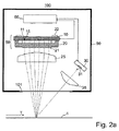
照明ユニット50は有価証券類を検査するために構成されるセンサ100に装備される(図2a参照)。照明ユニット50から放射される光は結像レンズ25によって有価証券類1上に結像される。そのようにする場合、有価証券類1はある領域にわたって一様な光強度で照明される。しかし、照明ユニット50によって放射される光を有価証券類1上に向けるために、結像レンズ25の代わりに、異なる光学コンポーネント、例えば、レンズシステム、回折光学コンポーネント、例えばフレネルレンズ、または結像ミラーを、結像光学系として用いることもできる。有価証券類1の光学特性に依存して、照明光の成分が有価証券類1によって反射される。有価証券類1から反射された光は、感光領域31を有する光検出ユニット30を用いて検出される。検出ユニット30は、例えばフォトダイオードまたはフォトトランジスタで形成することができる。必要に応じて、有価証券類1で反射された光を集光して感光領域31に向ける検出光学系35を検出ユニット30の前面に配置することができる。図示される例において、照明光は垂直方向で有価証券類1上に結像され、検出ユニット30は反射光を斜角方向で捕捉する。あるいは、照明を斜角方向で実施することもでき、検出ユニットは垂直方向で反射光を捕捉するかまたは斜角方向で反射光を補足することができる。
The
センサ100は、透明窓101がその下側に配置されているハウジング90を有する。照明ユニット50により放射される光は、搬送方向Tに沿って搬送されてセンサ100の下を通過する、検査されるべき有価証券類1上に窓101を通して結像される。照明ユニット50,詳しくは光源15,及び検出ユニット30は、本例においてはハウジング90内に配置されている、制御ユニット60によって駆動される。制御ユニット60は、例えばどの時点においても正確に1つの光源がオンに切り換えられるように、連続的に反復して光源15のオン/オフを切換える。光源のオン切換え段階中、検出ユニット30はそれぞれ、有価証券類1によって反射された光の強度に対応する1つの測定値を捕捉する。有価証券類1は相異なる光源15の相異なる発光スペクトルによって連続的に照明される。検出ユニット30はそれぞれ光源15による照明に同期して1つの測定値を検知するから、それぞれの光源15にあらかじめ定められたスペクトル領域において、有価証券類1によって反射された光の強度が測定される。
The
制御ユニット60は、光源15のオン/オフが切り換えられる照明シーケンスが周期的に反復するように光源15を駆動する。例えば、制御ユニット60は、照明ユニット50のそれぞれの光源15のオン/オフがそれぞれの照明シーケンス中に正確に1回切り換えられるように、プログラムすることができる。あるいは、光源15は、例えば低光度光源15の低強度を複数測定によって補償するため、照明シーケンス毎に数回駆動することもできる。照明シーケンスは、照明ユニット50に存在する全ての光源15の駆動、あるいは存在する光源15のサブセットだけの駆動を含むことができる。一照明シーケンス後、すなわち、その測定に対して与えられたそれぞれの発光スペクトルによる照明の下で測定値が検知された後、その測定に対して与えられたそれぞれの発光スペクトルによる照明の下で測定値が再び検知される、次の照明シーケンスが開始され、以下同様である。照明シーケンスの継続時間は、一照明シーケンスの相異なる測定値が有価証券類1上の少なくともほぼ同じ検出領域から得られるように、有価証券類1の搬送速度に整合される。したがって、同じ照明シーケンスの始めから終わりまでに有価証券類1がとる経路は検出領域の長さよりかなり短い。一照明シーケンス中に得られる測定値は、例えばそれぞれの検出領域の反射のスペクトル依存性を与えることができる。
The
センサ100は、光源支持手段10,マイクロレンズアレイ20,結像光学系25及び検出ユニット30を備えるセンサプラットフォーム70から作製される(図2b参照)。必要に応じて、センサプラットフォーム70は制御ユニット60及び/またはハウジング90及び/または検出光学系35を備える。しかし、本発明のセンサはこれらの要素が無くとも実現することができる。センサプラットフォーム70から、光源支持手段10に装着される光源15の選択に依存して、相異なるセンサが作製される。作製されるセンサによって満たされるべき要件に依存して、例えば第1のタイプのセンサ100Aまたは第2のタイプのセンサ100Bを同じセンサプラットフォーム70から作製することができる。
The
第1の実施形態例において、第1のタイプのセンサ100A及び第2のタイプのセンサ100Bには同じ選択Sの光源15が装着される(図3a参照)。センサ100A及び100Bのそれぞれの作製時にセンサプラットフォーム70に装着される選択Sの光源15は、図示される例において、14の相異なる光源15を有する。これらの光源15の相異なる発光ピークのスペクトル位置は図3aにおいてλ1からλ14として指定される。光源15の発光スペクトルは、例えば紫外スペクトル領域から可視スペクトル領域をわたって近赤外スペクトル領域まで広がる。しかし、第1のタイプのセンサ100A及び第2のタイプのセンサ100Bには、選択Sからの光源15の相異なるサブセットが用いられる。例えば、第1のタイプのセンサ100Aには、波長がλ1〜λ3,λ5,λ7及びλ9〜λ14の光源からなるサブセットAが用いられる(図3b参照)。第2のタイプのセンサ100Bには、波長がλ4〜λ10の光源からなるサブセットBが用いられる(図3c参照)。センサ100Aの制御ユニット60は、一照明シーケンス中に波長λ1〜λ3,λ5,λ7及びλ9〜λ14の光源のオン/オフが次々に切り換えられるように構成される。対照的に、第2のタイプのセンサ100Bの制御ユニット60は、第2のタイプのセンサ100Bの一照明シーケンス中に波長λ4〜λ10の光源のオン/オフが次々に切り換えられるように構成される。
In the first example embodiment, the
第2の実施形態例において、第2のタイプのセンサは第1のタイプのセンサ100Aに比較して異なる選択の光源を有する。したがってセンサプラットフォーム70には、第2のタイプのセンサ100Bを作製するため、センサ100Aの作製に比較して異なる選択の光源15が装着される。例えば、第1のタイプのセンサ100Aには第1の選択SAの光源15Aが装着され、第2のタイプのセンサ100Bには第2の選択SBの光源15Bが装着される(図4a及び4b参照)。本例において、第1の選択SAは、それぞれの波長がλ1〜λ10として指定される、10の相異なる光源15Aからなる。本例において、第2の選択SBは、それぞれの波長がλ10〜λ20として指定される、11の相異なる光源15Bからなる。ここで光源12Bは一部を光源12Aと同等とすることができる。
In the second example embodiment, the second type of sensor has a different selection of light sources compared to the first type of
1 有価証券類
10 光源支持手段
11 光源座
12 結合孔
15,15A,15B 光源
20 マイクロレンズアレイ
21 マイクロレンズ
22 結合ピン
25 結像レンズ
30 光検出ユニット
31 感光領域
35 検出光学系
50 照明ユニット
60 制御ユニット
70 センサプラットフォーム
90 ハウジング
100,100A,100B センサ
101 透明窓
DESCRIPTION OF SYMBOLS 1
Claims (13)
・複数の光源座(11)がその上に設けられる光源支持手段(10)であって、前記複数の光源座(11)のそれぞれは光源(15)を支持するために構成されるものである光源支持手段(10)、
・複数のマイクロレンズ(21)を有するマイクロレンズアレイ(20)であって、それによって、前記複数の光源座(11)のそれぞれが前記複数のマイクロレンズ(21)の内の正確に1つと対応付けられるように、前記光源支持手段(10)と、互いに対して配置することができるマイクロレンズアレイ(20)、
・結像光学系(25)、及び
・検出ユニット(30)、
を備える、センサプラットフォーム(70)を提供する工程、
照明ユニット(50)を、
・前記光源支持手段(10)に光源(15)を装着する工程であって、前記光源支持手段(10)の前記複数の光源座(11)の内のいくつかにはそれぞれ正確に1つの前記光源(15)が配置され、前記光源(15)の内の少なくとも2つの発光スペクトルが相異なるものである工程と、
・前記マイクロレンズアレイ(20)と、前記光源(15)が装着された、前記光源支持手段(10)を、前記光源(15)のそれぞれが前記マイクロレンズアレイ(20)の前記複数のマイクロレンズ(21)の内の正確に1つと対応付けられるように、互いに対して配置する工程と、
によって形成する工程、
前記照明ユニット(50)と前記結像光学系(25)を、前記センサ(100)の動作時に、前記照明ユニット(50)によって放射される光が前記センサ(100)によって検査されるべき有価証券類(1)上に前記結像光学系(25)により結像され得るように配置する工程、
前記検出ユニット(30)を、前記センサ(100)の動作時に、前記照明ユニット(50)によって照明された前記有価証券類(1)から発せられる検出光を前記検出ユニット(30)が検出できるように配置する工程、及び
前記光源(15)を駆動するために構成された制御ユニット(60)を前記センサ(100)に付与し、前記有価証券類(1)を相異なる発光スペクトルによって次々に照明できるように、前記照明ユニット(50)の前記光源(15)のオン/オフを次々に切り換えるために前記制御ユニット(60)を構成する工程
を含むことを特徴とする方法。 In a method of making a sensor (100) configured for inspection of securities,
A light source support means (10) provided thereon with a plurality of light source seats (11), each of the plurality of light source seats (11) being configured to support the light source (15). Light source support means (10),
A microlens array (20) having a plurality of microlenses (21), whereby each of the plurality of light source seats (11) corresponds to exactly one of the plurality of microlenses (21). As attached, the light source support means (10) and a microlens array (20) which can be arranged relative to each other,
An imaging optical system (25), and a detection unit (30),
Providing a sensor platform (70) comprising:
Lighting unit (50)
A step of mounting a light source (15) on the light source support means (10), wherein each of the plurality of light source seats (11) of the light source support means (10) has exactly one each A step in which a light source (15) is disposed and at least two of the light emission spectra of the light sources (15) are different from each other;
The microlens array (20) and the light source support means (10) on which the light source (15) is mounted, and each of the light sources (15) is the plurality of microlenses of the microlens array (20). Placing them relative to each other so as to be associated with exactly one of (21);
Forming by,
The illumination unit (50) and the imaging optical system (25) are provided with a security in which light emitted by the illumination unit (50) is to be inspected by the sensor (100) when the sensor (100) is operated. A step of arranging on the class (1) so as to be imaged by the imaging optical system (25) ;
The detection unit (30) can detect the detection light emitted from the securities (1) illuminated by the illumination unit (50) when the sensor (100) is operated. Placing in, and
The control unit (60) configured to drive the light source (15) is provided to the sensor (100) so that the securities (1) can be sequentially illuminated with different emission spectra. Configuring the control unit (60) to switch the light source (15) of the unit (50) on and off one after another .
・複数の光源座(11)がその上に設けられる光源支持手段(10)であって、前記複数の光源座(11)のそれぞれは光源(15)を支持するために構成されるものである光源支持手段(10)、
・複数のマイクロレンズ(21)を有するマイクロレンズアレイ(20)であって、それによって、前記複数の光源座(11)のそれぞれが前記複数のマイクロレンズ(21)の内の正確に1つと対応付けられるように、前記光源支持手段(10)と、互いに対して配置することができるマイクロレンズアレイ(20)、
・結像光学系(25)、及び
・検出ユニット(30)、
を備える、センサプラットフォーム(70)を提供する工程、
照明ユニット(50)を、
・前記光源支持手段(10)に光源(15)を装着する工程であって、前記光源支持手段(10)の前記複数の光源座(11)の内のいくつかにはそれぞれ正確に1つの前記光源(15)が配置され、前記光源(15)の内の少なくとも2つの発光スペクトルが相異なるものである工程と、
・前記マイクロレンズアレイ(20)と、前記光源(15)が装着された、前記光源支持手段(10)を、前記光源(15)のそれぞれが前記マイクロレンズアレイ(20)の前記複数のマイクロレンズ(21)の内の正確に1つと対応付けられるように、互いに対して配置する工程と、
によって形成する工程、
前記照明ユニット(50)と前記結像光学系(25)を、前記センサ(100)の動作時に、前記照明ユニット(50)によって放射される光が前記センサ(100)によって検査されるべき有価証券類(1)上に前記結像光学系(25)により結像され得るように配置する工程、及び
前記検出ユニット(30)を、前記センサ(100)の動作時に、前記照明ユニット(50)によって照明された前記有価証券類(1)から発せられる検出光を前記検出ユニット(30)が検出できるように配置する工程、
を含み、
有価証券類を検査するための相異なるセンサが、同じ前記センサプラットフォーム(70)から作製されることを特徴とする方法。 In a method of making a sensor (100) configured for inspection of securities,
A light source support means (10) provided thereon with a plurality of light source seats (11), each of the plurality of light source seats (11) being configured to support the light source (15). Light source support means (10),
A microlens array (20) having a plurality of microlenses (21), whereby each of the plurality of light source seats (11) corresponds to exactly one of the plurality of microlenses (21). As attached, the light source support means (10) and a microlens array (20) which can be arranged relative to each other,
An imaging optical system (25), and a detection unit (30),
Providing a sensor platform (70) comprising:
Lighting unit (50)
A step of mounting a light source (15) on the light source support means (10), wherein each of the plurality of light source seats (11) of the light source support means (10) has exactly one each A step in which a light source (15) is disposed and at least two of the light emission spectra of the light sources (15) are different from each other;
The microlens array (20) and the light source support means (10) on which the light source (15) is mounted, and each of the light sources (15) is the plurality of microlenses of the microlens array (20). Placing them relative to each other so as to be associated with exactly one of (21);
Forming by,
The illumination unit (50) and the imaging optical system (25) are provided with a security in which light emitted by the illumination unit (50) is to be inspected by the sensor (100) when the sensor (100) is operated. And a step of arranging the detection unit (30) on the class (1) so as to be imaged by the imaging optical system (25), and the illumination unit (50) during the operation of the sensor (100). Arranging the detection unit (30) so that the detection light emitted from the illuminated securities (1) can be detected;
Only including,
A method wherein different sensors for inspecting securities are made from the same sensor platform (70) .
照明ユニット(50)であって、
・それぞれの発光スペクトルが相異なる、少なくとも2つの光源(15)と、
・それぞれが前記光源(15)の内の1つを支持するために構成された、複数の光源座(11)がその上に設けられる光源支持手段(10)であって、前記光源座(11)のいくつかにおいて、それぞれに前記光源(15)の内の1つが正確に配置される光源支持手段(10)と、
・複数のマイクロレンズ(21)を有するマイクロレンズアレイ(20)であって、前記マイクロレンズアレイ(20)及び前記光源支持手段(10)は、前記光源支持手段(10)上に配置された前記光源(15)のそれぞれが前記複数のマイクロレンズ(21)の内の正確に1つと対応付けられ、よって前記光源(15)のそれぞれの発光光が前記光源(15)と対応付けられた前記マイクロレンズ(21)によって集光されるように、互いに対して配置されるものであるマイクロレンズアレイ(20)と、
を有する照明ユニット(50)、
前記照明ユニット(50)によって放射される光を、前記センサ(100)の動作時に、前記センサ(100)によって捕捉されるべき有価証券類(1)上に結像させることができる、結像光学系(25)、
前記センサ(100)の動作時に、前記照明ユニット(50)によって照明された前記有価証券類(1)から発せられる検出光を検出するために構成された検出ユニット(30)、及び
前記有価証券類(1)を相異なる発光スペクトルによって次々に照明するために前記照明ユニット(50)の前記光源(15)のオン/オフを次々に切り換えるように適合された制御ユニット(60)
を備えることを特徴とするセンサ(100)。 In the sensor (100) for inspecting securities,
A lighting unit (50),
At least two light sources (15), each having a different emission spectrum;
A light source support means (10) on which a plurality of light source seats (11), each of which is configured to support one of the light sources (15), the light source seat (11 ), A light source support means (10) in which one of the light sources (15) is precisely positioned,
A microlens array (20) having a plurality of microlenses (21), wherein the microlens array (20) and the light source support means (10) are disposed on the light source support means (10). Each of the light sources (15) is associated with exactly one of the plurality of microlenses (21), and thus each of the light emitted from the light source (15) is associated with the light source (15). A microlens array (20) that is arranged relative to each other so as to be focused by a lens (21);
A lighting unit (50) having
Imaging optics capable of imaging light emitted by the illumination unit (50) onto securities (1) to be captured by the sensor (100) during operation of the sensor (100) System (25) ,
A detection unit (30) configured to detect detection light emitted from the securities (1) illuminated by the illumination unit (50) during operation of the sensor (100); and
A control unit (60) adapted to turn on / off the light source (15) of the lighting unit (50) one after another in order to illuminate the securities (1) one after another with different emission spectra.
A sensor (100) comprising:
照明ユニット(50)であって、
・それぞれの発光スペクトルが相異なる、少なくとも2つの光源(15)と、
・それぞれが前記光源(15)の内の1つを支持するために構成された、複数の光源座(11)がその上に設けられる光源支持手段(10)であって、前記光源座(11)のいくつかにおいて、それぞれに前記光源(15)の内の1つが正確に配置される光源支持手段(10)と、
・複数のマイクロレンズ(21)を有するマイクロレンズアレイ(20)であって、前記マイクロレンズアレイ(20)及び前記光源支持手段(10)は、前記光源支持手段(10)上に配置された前記光源(15)のそれぞれが前記複数のマイクロレンズ(21)の内の正確に1つと対応付けられ、よって前記光源(15)のそれぞれの発光光が前記光源(15)と対応付けられた前記マイクロレンズ(21)によって集光されるように、互いに対して配置されるものであるマイクロレンズアレイ(20)と、
を有する照明ユニット(50)、
前記照明ユニット(50)によって放射される光を、前記センサ(100)の動作時に、前記センサ(100)によって捕捉されるべき有価証券類(1)上に結像させることができる、結像光学系(25)、及び
前記センサ(100)の動作時に、前記照明ユニット(50)によって照明された前記有価証券類(1)から発せられる検出光を検出するために構成された検出ユニット(30)、
を備え、
当該センサ(100)が、前記センサ(100)の動作時に、前記有価証券類(1)から発せられる光のスペクトル強度分布を捕捉するためにオン/オフが次々に切り換えられる、複数の相異なる光源(15)を備えていることを特徴とするセンサ(100)。 In the sensor (100) for inspecting securities,
A lighting unit (50),
At least two light sources (15), each having a different emission spectrum;
A light source support means (10) on which a plurality of light source seats (11), each of which is configured to support one of the light sources (15), the light source seat (11 ), A light source support means (10) in which one of the light sources (15) is precisely positioned,
A microlens array (20) having a plurality of microlenses (21), wherein the microlens array (20) and the light source support means (10) are disposed on the light source support means (10). Each of the light sources (15) is associated with exactly one of the plurality of microlenses (21), and thus each of the light emitted from the light source (15) is associated with the light source (15). A microlens array (20) that is arranged relative to each other so as to be focused by a lens (21);
A lighting unit (50) having
Imaging optics capable of imaging light emitted by the illumination unit (50) onto securities (1) to be captured by the sensor (100) during operation of the sensor (100) A detection unit (30) configured to detect detection light emitted from the securities (1) illuminated by the illumination unit (50) during operation of the system (25) and the sensor (100); ,
Equipped with a,
A plurality of different light sources that are switched on and off one after another in order for the sensor (100) to capture the spectral intensity distribution of light emitted from the securities (1) during operation of the sensor (100) A sensor (100) characterized by comprising (15 ).
前記少なくとも1つの第1のタイプのセンサ(100A)及び前記少なくとも1つの第2のタイプのセンサ(100B)がそれぞれ、
照明ユニット(50)であって、
・それぞれの発光スペクトルが相異なる、少なくとも2つの光源(15)と、
・それぞれが前記光源(15)の内の1つを支持するために構成された、複数の光源座(11)がその上に設けられる光源支持手段(10)であって、前記光源座(11)のいくつかにおいて、それぞれに前記光源(15)の内の1つが正確に配置される光源支持手段(10)と、
・複数のマイクロレンズ(21)を有するマイクロレンズアレイ(20)であって、前記マイクロレンズアレイ(20)及び前記光源支持手段(10)は、前記光源支持手段(10)上に配置された前記光源(15)のそれぞれが前記複数のマイクロレンズ(21)の内の正確に1つと対応付けられ、よって前記光源(15)のそれぞれの発光光が前記光源(15)と対応付けられた前記マイクロレンズ(21)によって集光されるように、互いに対して配置されるものであるマイクロレンズアレイ(20)と、
を有する照明ユニット(50)、
前記照明ユニット(50)によって放射される光を、前記センサ(100)の動作時に、前記センサ(100)によって捕捉されるべき有価証券類(1)上に結像させることができる、結像光学系(25)、及び
前記センサ(100)の動作時に、前記照明ユニット(50)によって照明された前記有価証券類(1)から発せられる検出光を検出するために構成された検出ユニット(30)、
を備え、
前記少なくとも1つの第1のタイプのセンサ(100A)がいくつかの第1の発光スペクトルを用いる照射によって有価証券類を検査するために構成され、前記少なくとも1つの第2のタイプのセンサ(100B)が、少なくとも1つが前記第1の発光スペクトルとは異なる、いくつかの第2の発光スペクトルを用いる照射によって有価証券類を検査するために構成されることを特徴とするセンサファミリー。 A sensor family comprising at least one first type sensor (100A) and at least one second type sensor (100B), comprising:
The at least one first type sensor (100A) and the at least one second type sensor (100B), respectively,
A lighting unit (50),
At least two light sources (15), each having a different emission spectrum;
A light source support means (10) on which a plurality of light source seats (11), each of which is configured to support one of the light sources (15), the light source seat (11 ), A light source support means (10) in which one of the light sources (15) is precisely positioned,
A microlens array (20) having a plurality of microlenses (21), wherein the microlens array (20) and the light source support means (10) are disposed on the light source support means (10). Each of the light sources (15) is associated with exactly one of the plurality of microlenses (21), and thus each of the light emitted from the light source (15) is associated with the light source (15). A microlens array (20) that is arranged relative to each other so as to be focused by a lens (21);
A lighting unit (50) having
Imaging optics capable of imaging light emitted by the illumination unit (50) onto securities (1) to be captured by the sensor (100) during operation of the sensor (100) System (25), and
A detection unit (30) configured to detect detection light emitted from the securities (1) illuminated by the illumination unit (50) during operation of the sensor (100);
With
The at least one first type sensor (100A) is configured for inspecting securities by irradiation with a number of first emission spectra, and the at least one second type sensor (100B) A sensor family, wherein at least one sensor is configured to inspect securities by irradiation with a number of second emission spectra different from the first emission spectrum.
Applications Claiming Priority (3)
| Application Number | Priority Date | Filing Date | Title |
|---|---|---|---|
| DE102009058804A DE102009058804A1 (en) | 2009-12-18 | 2009-12-18 | Sensor for checking value documents |
| DE102009058804.3 | 2009-12-18 | ||
| PCT/EP2010/007703 WO2011072862A1 (en) | 2009-12-18 | 2010-12-16 | Sensor for checking value documents |
Publications (3)
| Publication Number | Publication Date |
|---|---|
| JP2013514566A JP2013514566A (en) | 2013-04-25 |
| JP2013514566A5 JP2013514566A5 (en) | 2013-10-10 |
| JP5615935B2 true JP5615935B2 (en) | 2014-10-29 |
Family
ID=43709179
Family Applications (1)
| Application Number | Title | Priority Date | Filing Date |
|---|---|---|---|
| JP2012543526A Active JP5615935B2 (en) | 2009-12-18 | 2010-12-16 | Sensor for inspecting securities |
Country Status (7)
| Country | Link |
|---|---|
| US (1) | US8749768B2 (en) |
| EP (1) | EP2513873B1 (en) |
| JP (1) | JP5615935B2 (en) |
| KR (1) | KR101841301B1 (en) |
| DE (1) | DE102009058804A1 (en) |
| ES (1) | ES2827182T3 (en) |
| WO (1) | WO2011072862A1 (en) |
Families Citing this family (12)
| Publication number | Priority date | Publication date | Assignee | Title |
|---|---|---|---|---|
| CN102913810A (en) * | 2011-08-01 | 2013-02-06 | 吉鸿电子股份有限公司 | Identification device and light source module thereof |
| EP2568444B1 (en) * | 2011-09-12 | 2017-11-01 | International Currency Technologies Corporation | Validation apparatus and light source module thereof |
| JP6502630B2 (en) * | 2013-09-30 | 2019-04-17 | 株式会社リコー | Optical sensor, optical inspection apparatus, and optical characteristic detection method |
| DE102014105746C5 (en) * | 2013-12-05 | 2020-12-24 | Sick Ag | Optoelectronic sensor and method for detecting shiny objects |
| CN103791452B (en) * | 2014-02-21 | 2017-01-04 | 中国人民银行印制科学技术研究所 | Light-source system |
| US10509147B2 (en) | 2015-01-29 | 2019-12-17 | ams Sensors Singapore Pte. Ltd | Apparatus for producing patterned illumination using arrays of light sources and lenses |
| US9273846B1 (en) * | 2015-01-29 | 2016-03-01 | Heptagon Micro Optics Pte. Ltd. | Apparatus for producing patterned illumination including at least one array of light sources and at least one array of microlenses |
| US11728356B2 (en) * | 2015-05-14 | 2023-08-15 | Semiconductor Energy Laboratory Co., Ltd. | Photoelectric conversion element and imaging device |
| CN108779905B (en) * | 2016-01-26 | 2021-08-20 | 新加坡恒立私人有限公司 | Multi-mode lighting module and related methods |
| WO2018000036A1 (en) | 2016-07-01 | 2018-01-04 | Cylite Pty Ltd | Apparatus and method for confocal microscopy using dispersed structured illumination |
| EP3503049B1 (en) * | 2017-12-22 | 2021-02-24 | CI Tech Sensors AG | Device and method for detecting a machine-readable security feature of a valuable document |
| US11085609B1 (en) * | 2021-02-08 | 2021-08-10 | Himax Technologies Limited | Illumination device |
Family Cites Families (18)
| Publication number | Priority date | Publication date | Assignee | Title |
|---|---|---|---|---|
| US3743422A (en) * | 1970-06-18 | 1973-07-03 | Westinghouse Electric Corp | Optical image processor |
| US3765749A (en) * | 1972-05-23 | 1973-10-16 | Bell Telephone Labor Inc | Optical memory storage and retrieval system |
| EP0198819B1 (en) | 1983-12-27 | 1988-08-24 | BERGSTRÖM, Arne | Apparatus for authenticating bank notes |
| US5875259A (en) * | 1990-02-05 | 1999-02-23 | Cummins-Allison Corp. | Method and apparatus for discriminating and counting documents |
| CA2169865C (en) * | 1996-02-20 | 2007-07-03 | Vitold A. Khvostov | Optical reflection sensing arrangement for scanning devices |
| US5923413A (en) | 1996-11-15 | 1999-07-13 | Interbold | Universal bank note denominator and validator |
| DE10027726A1 (en) * | 2000-06-03 | 2001-12-06 | Bundesdruckerei Gmbh | Sensor for the authenticity detection of signets on documents |
| GB2366371A (en) * | 2000-09-04 | 2002-03-06 | Mars Inc | Sensing documents such as currency items |
| US7221512B2 (en) * | 2002-01-24 | 2007-05-22 | Nanoventions, Inc. | Light control material for displaying color information, and images |
| JP2005276849A (en) * | 2004-02-24 | 2005-10-06 | Ricoh Co Ltd | Led array element, method of manufacturing microlens array thereof optical writing device, and optical reader |
| DE102004021397A1 (en) | 2004-04-30 | 2005-11-24 | Bundesdruckerei Gmbh | Apparatus and method for checking the authenticity of a provided with a security feature security or value document that is applied to a support |
| JP2006058488A (en) | 2004-08-18 | 2006-03-02 | Nippon Sheet Glass Co Ltd | Illumination optical device and projection type display device using the same |
| DE102005029119A1 (en) | 2005-06-23 | 2006-12-28 | Carl Zeiss Jena Gmbh | Illumination device, especially for microscopes, has individual light sources designed as discrete cells |
| US7715001B2 (en) * | 2006-02-13 | 2010-05-11 | Pacific Biosciences Of California, Inc. | Methods and systems for simultaneous real-time monitoring of optical signals from multiple sources |
| WO2008024863A2 (en) * | 2006-08-22 | 2008-02-28 | Mei, Inc. | Optical detector arrangement for document acceptor |
| US7489456B2 (en) * | 2007-05-02 | 2009-02-10 | International Currency Technologies Corporation | Lens module |
| DE102007031230B3 (en) | 2007-07-04 | 2008-10-30 | Bundesdruckerei Gmbh | Document capture system and document capture process |
| DE202007013090U1 (en) * | 2007-09-19 | 2007-12-13 | International Currency Technologies Corporation | Anti-EMI lens module |
-
2009
- 2009-12-18 DE DE102009058804A patent/DE102009058804A1/en not_active Withdrawn
-
2010
- 2010-12-16 ES ES10792845T patent/ES2827182T3/en active Active
- 2010-12-16 KR KR1020127018659A patent/KR101841301B1/en active IP Right Grant
- 2010-12-16 US US13/515,720 patent/US8749768B2/en active Active
- 2010-12-16 WO PCT/EP2010/007703 patent/WO2011072862A1/en active Application Filing
- 2010-12-16 EP EP10792845.9A patent/EP2513873B1/en active Active
- 2010-12-16 JP JP2012543526A patent/JP5615935B2/en active Active
Also Published As
| Publication number | Publication date |
|---|---|
| ES2827182T3 (en) | 2021-05-20 |
| KR20120105525A (en) | 2012-09-25 |
| DE102009058804A1 (en) | 2011-06-22 |
| WO2011072862A1 (en) | 2011-06-23 |
| KR101841301B1 (en) | 2018-03-22 |
| EP2513873A1 (en) | 2012-10-24 |
| US20120257191A1 (en) | 2012-10-11 |
| US8749768B2 (en) | 2014-06-10 |
| EP2513873B1 (en) | 2020-10-07 |
| JP2013514566A (en) | 2013-04-25 |
Similar Documents
| Publication | Publication Date | Title |
|---|---|---|
| JP5615935B2 (en) | Sensor for inspecting securities | |
| JP5662469B2 (en) | Spectrum sensor for inspection of securities | |
| AU2009259721B2 (en) | Sensor device for the spectrally resolved capture of valuable documents and a corresponding method | |
| JP5822837B2 (en) | Document sensor | |
| US8817242B2 (en) | Sensor device for the spectrally resolved capture of valuable documents and a corresponding method | |
| US8482816B2 (en) | Document acquisition system and document acquisition method | |
| US8115910B2 (en) | Apparatus and method for the optical examination of value documents | |
| JP6469370B2 (en) | Optical line sensor device | |
| JP2009153149A (en) | Device for acquisition of image of predetermined section of moving print product, and method of operating the same | |
| JP2013514566A5 (en) | ||
| JP6775421B2 (en) | Measurement optics and methods using illumination pattern formation | |
| EP1861683A1 (en) | Apparatus and method for collecting and detecting light emitted by a lighting apparatus | |
| US8662278B2 (en) | Sensor for checking value documents | |
| CN114502930A (en) | Detector array and spectrometer system | |
| JP5820845B2 (en) | Illumination device, image sensor unit, and paper sheet identification device | |
| JP2004222284A (en) | Improvement of scanning head | |
| JPH0954850A (en) | Paper money discrimination device | |
| JP7106674B2 (en) | Spectrometer | |
| JP7106673B2 (en) | Spectrometer | |
| JP7050601B2 (en) | Lighting method, imaging method, lighting device and imaging device | |
| JP2022155138A (en) | identification device | |
| CN116348756A (en) | Device and method for the transmission inspection of containers having at least one light-emitting diode light source |
Legal Events
| Date | Code | Title | Description |
|---|---|---|---|
| A521 | Request for written amendment filed |
Free format text: JAPANESE INTERMEDIATE CODE: A523 Effective date: 20130823 |
|
| A621 | Written request for application examination |
Free format text: JAPANESE INTERMEDIATE CODE: A621 Effective date: 20130823 |
|
| A977 | Report on retrieval |
Free format text: JAPANESE INTERMEDIATE CODE: A971007 Effective date: 20140417 |
|
| A131 | Notification of reasons for refusal |
Free format text: JAPANESE INTERMEDIATE CODE: A131 Effective date: 20140422 |
|
| A521 | Request for written amendment filed |
Free format text: JAPANESE INTERMEDIATE CODE: A523 Effective date: 20140722 |
|
| TRDD | Decision of grant or rejection written | ||
| A01 | Written decision to grant a patent or to grant a registration (utility model) |
Free format text: JAPANESE INTERMEDIATE CODE: A01 Effective date: 20140819 |
|
| A61 | First payment of annual fees (during grant procedure) |
Free format text: JAPANESE INTERMEDIATE CODE: A61 Effective date: 20140910 |
|
| R150 | Certificate of patent or registration of utility model |
Ref document number: 5615935 Country of ref document: JP Free format text: JAPANESE INTERMEDIATE CODE: R150 |
|
| R250 | Receipt of annual fees |
Free format text: JAPANESE INTERMEDIATE CODE: R250 |
|
| S111 | Request for change of ownership or part of ownership |
Free format text: JAPANESE INTERMEDIATE CODE: R313113 |
|
| R350 | Written notification of registration of transfer |
Free format text: JAPANESE INTERMEDIATE CODE: R350 |
|
| R250 | Receipt of annual fees |
Free format text: JAPANESE INTERMEDIATE CODE: R250 |
|
| R250 | Receipt of annual fees |
Free format text: JAPANESE INTERMEDIATE CODE: R250 |
|
| R250 | Receipt of annual fees |
Free format text: JAPANESE INTERMEDIATE CODE: R250 |
|
| R250 | Receipt of annual fees |
Free format text: JAPANESE INTERMEDIATE CODE: R250 |
|
| R250 | Receipt of annual fees |
Free format text: JAPANESE INTERMEDIATE CODE: R250 |
|
| R250 | Receipt of annual fees |
Free format text: JAPANESE INTERMEDIATE CODE: R250 |