JP5612613B2 - Multicolor electronic device and method for forming it by printing - Google Patents
Multicolor electronic device and method for forming it by printing Download PDFInfo
- Publication number
- JP5612613B2 JP5612613B2 JP2011553162A JP2011553162A JP5612613B2 JP 5612613 B2 JP5612613 B2 JP 5612613B2 JP 2011553162 A JP2011553162 A JP 2011553162A JP 2011553162 A JP2011553162 A JP 2011553162A JP 5612613 B2 JP5612613 B2 JP 5612613B2
- Authority
- JP
- Japan
- Prior art keywords
- subpixel
- row
- printing
- rows
- workpiece
- Prior art date
- Legal status (The legal status is an assumption and is not a legal conclusion. Google has not performed a legal analysis and makes no representation as to the accuracy of the status listed.)
- Expired - Fee Related
Links
Images


Classifications
-
- G—PHYSICS
- G02—OPTICS
- G02B—OPTICAL ELEMENTS, SYSTEMS OR APPARATUS
- G02B5/00—Optical elements other than lenses
- G02B5/20—Filters
- G02B5/201—Filters in the form of arrays
-
- B—PERFORMING OPERATIONS; TRANSPORTING
- B41—PRINTING; LINING MACHINES; TYPEWRITERS; STAMPS
- B41J—TYPEWRITERS; SELECTIVE PRINTING MECHANISMS, i.e. MECHANISMS PRINTING OTHERWISE THAN FROM A FORME; CORRECTION OF TYPOGRAPHICAL ERRORS
- B41J2/00—Typewriters or selective printing mechanisms characterised by the printing or marking process for which they are designed
- B41J2/005—Typewriters or selective printing mechanisms characterised by the printing or marking process for which they are designed characterised by bringing liquid or particles selectively into contact with a printing material
- B41J2/01—Ink jet
- B41J2/135—Nozzles
- B41J2/14—Structure thereof only for on-demand ink jet heads
-
- G—PHYSICS
- G02—OPTICS
- G02B—OPTICAL ELEMENTS, SYSTEMS OR APPARATUS
- G02B5/00—Optical elements other than lenses
- G02B5/20—Filters
- G02B5/22—Absorbing filters
- G02B5/223—Absorbing filters containing organic substances, e.g. dyes, inks or pigments
-
- G—PHYSICS
- G02—OPTICS
- G02F—OPTICAL DEVICES OR ARRANGEMENTS FOR THE CONTROL OF LIGHT BY MODIFICATION OF THE OPTICAL PROPERTIES OF THE MEDIA OF THE ELEMENTS INVOLVED THEREIN; NON-LINEAR OPTICS; FREQUENCY-CHANGING OF LIGHT; OPTICAL LOGIC ELEMENTS; OPTICAL ANALOGUE/DIGITAL CONVERTERS
- G02F1/00—Devices or arrangements for the control of the intensity, colour, phase, polarisation or direction of light arriving from an independent light source, e.g. switching, gating or modulating; Non-linear optics
- G02F1/01—Devices or arrangements for the control of the intensity, colour, phase, polarisation or direction of light arriving from an independent light source, e.g. switching, gating or modulating; Non-linear optics for the control of the intensity, phase, polarisation or colour
- G02F1/13—Devices or arrangements for the control of the intensity, colour, phase, polarisation or direction of light arriving from an independent light source, e.g. switching, gating or modulating; Non-linear optics for the control of the intensity, phase, polarisation or colour based on liquid crystals, e.g. single liquid crystal display cells
- G02F1/133—Constructional arrangements; Operation of liquid crystal cells; Circuit arrangements
- G02F1/1333—Constructional arrangements; Manufacturing methods
- G02F1/1335—Structural association of cells with optical devices, e.g. polarisers or reflectors
- G02F1/133509—Filters, e.g. light shielding masks
- G02F1/133514—Colour filters
-
- H—ELECTRICITY
- H10—SEMICONDUCTOR DEVICES; ELECTRIC SOLID-STATE DEVICES NOT OTHERWISE PROVIDED FOR
- H10K—ORGANIC ELECTRIC SOLID-STATE DEVICES
- H10K71/00—Manufacture or treatment specially adapted for the organic devices covered by this subclass
- H10K71/10—Deposition of organic active material
- H10K71/12—Deposition of organic active material using liquid deposition, e.g. spin coating
- H10K71/13—Deposition of organic active material using liquid deposition, e.g. spin coating using printing techniques, e.g. ink-jet printing or screen printing
- H10K71/135—Deposition of organic active material using liquid deposition, e.g. spin coating using printing techniques, e.g. ink-jet printing or screen printing using ink-jet printing
-
- G—PHYSICS
- G02—OPTICS
- G02F—OPTICAL DEVICES OR ARRANGEMENTS FOR THE CONTROL OF LIGHT BY MODIFICATION OF THE OPTICAL PROPERTIES OF THE MEDIA OF THE ELEMENTS INVOLVED THEREIN; NON-LINEAR OPTICS; FREQUENCY-CHANGING OF LIGHT; OPTICAL LOGIC ELEMENTS; OPTICAL ANALOGUE/DIGITAL CONVERTERS
- G02F1/00—Devices or arrangements for the control of the intensity, colour, phase, polarisation or direction of light arriving from an independent light source, e.g. switching, gating or modulating; Non-linear optics
- G02F1/01—Devices or arrangements for the control of the intensity, colour, phase, polarisation or direction of light arriving from an independent light source, e.g. switching, gating or modulating; Non-linear optics for the control of the intensity, phase, polarisation or colour
- G02F1/13—Devices or arrangements for the control of the intensity, colour, phase, polarisation or direction of light arriving from an independent light source, e.g. switching, gating or modulating; Non-linear optics for the control of the intensity, phase, polarisation or colour based on liquid crystals, e.g. single liquid crystal display cells
- G02F1/133—Constructional arrangements; Operation of liquid crystal cells; Circuit arrangements
- G02F1/1333—Constructional arrangements; Manufacturing methods
- G02F1/1335—Structural association of cells with optical devices, e.g. polarisers or reflectors
- G02F1/133509—Filters, e.g. light shielding masks
- G02F1/133514—Colour filters
- G02F1/133516—Methods for their manufacture, e.g. printing, electro-deposition or photolithography
Landscapes
- Physics & Mathematics (AREA)
- General Physics & Mathematics (AREA)
- Optics & Photonics (AREA)
- Nonlinear Science (AREA)
- Engineering & Computer Science (AREA)
- Manufacturing & Machinery (AREA)
- Mathematical Physics (AREA)
- Chemical & Material Sciences (AREA)
- Crystallography & Structural Chemistry (AREA)
- Electroluminescent Light Sources (AREA)
- Ink Jet (AREA)
Description
[関連出願の相互参照]
本出願は、全体が参照により本明細書中に援用されている2009年3月6日出願の仮特許出願第61/158,017号からの優先権を、35.U.S.C.第119条(e)に基づき主張するものである。
[Cross-reference of related applications]
This application claims priority from provisional patent application No. 61 / 158,017 filed Mar. 6, 2009, which is incorporated herein by reference in its entirety. U. S. C. Claims based on Article 119 (e).
本開示は一般に、電子デバイスおよび方法、そしてより詳細には、電極および異なる色の有機活性領域を有する電子デバイス、ならびにこれを形成する方法に関する。 The present disclosure relates generally to electronic devices and methods, and more particularly to electronic devices having electrodes and organic active regions of different colors, and methods of forming the same.
電子デバイスは、液晶ディスプレイ(「LCD」)、有機発光ダイオード(OLED)ディスプレイなどを含み得る。電子デバイスの製造は、溶液堆積技術を用いて実施されてもよい。電子デバイスを製造する1つの方法は、印刷(例えばインクジェット印刷、連続印刷など)により基板上に有機層を堆積させることにある。印刷プロセスにおいて、印刷されている液体組成物は、有機溶媒、水性溶媒または溶媒の組合せを用いた溶液、分散体、エマルジョンまたは懸濁液の形で有機材料を含む。印刷の後、1つまたは複数の溶媒は蒸発させられ、有機材料が残って電子デバイスのための有機層を形成する。 Electronic devices may include liquid crystal displays (“LCD”), organic light emitting diode (OLED) displays, and the like. Electronic device manufacturing may be performed using solution deposition techniques. One method of manufacturing an electronic device is to deposit an organic layer on a substrate by printing (eg, ink jet printing, continuous printing, etc.). In the printing process, the liquid composition being printed comprises the organic material in the form of a solution, dispersion, emulsion or suspension using an organic solvent, an aqueous solvent or a combination of solvents. After printing, one or more solvents are evaporated, leaving the organic material to form an organic layer for the electronic device.
典型的には、第1の色が印刷され、その後印刷装置が再較正され、第2の色が印刷される。一部の場合、第1の印刷された色を伴う基板は、第2の色の印刷のために第2のプリンタまで移動される。これには同様に、プリンタの設定および整列のための時間も必要である。多くの場合において、赤、緑および青の3つの色が印刷される。この場合、各色について再較正および/または再整列の時間をかけなくてはならない。改善された印刷プロセスに対するニーズが存在する。 Typically, the first color is printed, after which the printing device is recalibrated and the second color is printed. In some cases, the substrate with the first printed color is moved to the second printer for printing the second color. This also requires time for printer setup and alignment. In many cases, three colors are printed: red, green and blue. In this case, recalibration and / or realignment time must be taken for each color. There is a need for an improved printing process.
加工物上に規則的アレイをサブピクセル行印刷するための方法において、サブピクセルがc種類の異なる色を有しかつサブピクセルピッチsを有する方法であって、
(a) pというノズル間間隔を伴って行の形で配置されたz個のノズルを有するプリントヘッドを提供するステップであって、z=n1(c)、p=(c−1)(s)であり、プリントヘッドが加工物に対して第1の位置にあるステップと;
(b) c種類の色の各々について1つずつのc種類の異なる印刷用インクを提供するステップと;
(c) 規則的な交互パターンでノズルに印刷用インクの各々を供給するステップと;
(d) プリントヘッドでz行のサブピクセルの第1のセットを印刷するステップと;
(e) プリントヘッドに対して横方向に加工物を距離d1だけ移動させるステップであって、d1=z(s)であるステップと;
(f) プリントヘッドでz行のサブピクセルの第2のセットを印刷するステップと;
(g) z行のサブピクセルを合計で(n2+2)セットのために、(e)ステップおよび(f)ステップをn2回反復するステップと、
を含み、
cは、1より大きい整数であり;
n1は、cが奇数である場合にはn1も奇数であることを条件として、0より大きい整数であり;
n2は0よりも大きい整数である、
方法が提供されている。
A method for printing a regular array of subpixel rows on a workpiece, wherein the subpixel has c different colors and has a subpixel pitch s, comprising:
(A) providing a printhead having z nozzles arranged in rows with an inter-nozzle spacing of p, where z = n 1 (c), p = (c−1) ( s) and the print head is in a first position relative to the workpiece;
(B) providing c different printing inks, one for each of the c colors;
(C) supplying each of the printing inks to the nozzles in a regular alternating pattern;
(D) printing a first set of z rows of sub-pixels with a printhead;
(E) moving the workpiece laterally relative to the print head by a distance d 1 , where d 1 = z (s);
(F) printing a second set of z-row sub-pixels with a printhead;
(G) repeating the steps (e) and (f) n 2 times for a total of (n 2 +2) sets of z rows of subpixels;
Including
c is an integer greater than 1;
n 1 is an integer greater than 0, provided that if c is odd, n 1 is also odd;
n 2 is an integer greater than 0,
A method is provided.
以上の一般的記述および以下の詳細な記述は単に例示および説明を目的としたものにすぎず、添付のクレームに定義されている通りの発明を限定するものではない。 The foregoing general description and the following detailed description are exemplary and explanatory only and are not restrictive of the invention as defined in the appended claims.
本明細書中で提示されている概念をよりよく理解するために、添付の図中に実施形態が示されている。 For a better understanding of the concepts presented herein, embodiments are shown in the accompanying figures.
当業者であれば、図中の要素が簡略化および明確化を期して示されたものであり、必ずしも原寸に比例して描かれているわけではないということがわかる。例えば、図中の一部の要素の寸法は、本発明の実施形態をより良く理解する一助となるように、他の要素に比べて誇張されていることがある。 Those skilled in the art will appreciate that the elements in the figures are shown for simplicity and clarity and are not necessarily drawn to scale. For example, the dimensions of some elements in the figures may be exaggerated relative to other elements to help better understand the embodiments of the present invention.
以上では数多くの態様および実施形態を記述してきたが、これらは単に例示的なものであり非限定的である。本明細書を読んだ後、当業者であれば、本発明の範囲から逸脱することなく他の態様および実施形態が可能であるということがわかる。 Although a number of aspects and embodiments have been described above, these are merely exemplary and not limiting. After reading this specification, skilled artisans will appreciate that other aspects and embodiments are possible without departing from the scope of the invention.
実施形態のうちのいずれか1つの実施形態の他の特徴および利益が、以下の詳細な説明およびクレームから明らかとなる。詳細な説明は、まず最初に「用語の定義と明確化」そしてそれに続く「プリンタ」「印刷方法」および「電子デバイス」を扱うものである。 Other features and benefits of any one of the embodiments will be apparent from the following detailed description and claims. The detailed description will first deal with "Term Definition and Clarification", followed by "Printer", "Printing Method" and "Electronic Device".
1.用語の定義および明確化
以下で記述する実施形態の詳細に触れる前に、いくつかの用語を定義づけし明確化する。
1. Definition and Clarification of Terms Before addressing details of the embodiments described below, some terms are defined and clarified.
「アレイ」という用語は、要素の秩序立った配置を意味するように意図されている。アレイは、ピクセル、サブピクセル、セルまたは通常行および列と呼ばれる秩序立った配置内のその他の構造を含んでいて良い。アレイを、x方向およびy方向の観点から記述することができる。 The term “array” is intended to mean an ordered arrangement of elements. The array may include pixels, sub-pixels, cells or other structures in an ordered arrangement usually referred to as rows and columns. An array can be described in terms of x and y directions.
「青色発光部品」という用語は、およそ400〜500nmの範囲内の波長で発光極大を有する放射線を発することのできる電子部品を意味するように意図されている。 The term “blue light-emitting component” is intended to mean an electronic component capable of emitting radiation having an emission maximum at a wavelength in the range of approximately 400-500 nm.
「連続的」という用語およびその変形形態は、実質的に切れ目がないことを意味するように意図されている。一実施形態において、連続的に印刷することは、液滴を用いた堆積技術とは対照的に、液体または液体組成物の実質的に切れ目のない流れを用いて印刷することである。別の実施形態においては、「連続的に延在する」とは、その一定長に沿って層、部材または構造内に有意な破断が一切無い、一定長の層、部材または構造を意味する。 The term “continuous” and variations thereof are intended to mean substantially unbroken. In one embodiment, continuous printing is printing using a substantially unbroken stream of liquid or liquid composition as opposed to deposition techniques using droplets. In another embodiment, “continuously extending” means a layer, member or structure of a certain length without any significant breaks in the layer, member or structure along that length.
「電子デバイス」という用語は、適切に電気接続され適切な電位が供給された場合に集合的に1つの機能を果たす回路、電子部品またはその任意の組合せの集合物を意味するように意図されている。電子デバイスは、1つのシステム内に含まれていても、またはその一部をなしていてもよい。電子デバイスの一例としては、ディスプレイ、センサーアレイ、コンピュータシステム、航空電子システム、自動車、携帯電話、その他の民生用または工業用電子製品、またはその任意の組合せが含まれる。 The term “electronic device” is intended to mean a collection of circuits, electronic components, or any combination thereof that collectively perform a function when properly electrically connected and supplied with an appropriate potential. Yes. The electronic device may be included in or part of one system. Examples of electronic devices include displays, sensor arrays, computer systems, avionic systems, automobiles, cell phones, other consumer or industrial electronic products, or any combination thereof.
「緑色発光部品」という用語は、およそ500〜600nmの範囲内の波長で発光極大を有する放射線を発することのできる電子部品を意味するように意図されている。 The term “green light-emitting component” is intended to mean an electronic component capable of emitting radiation having an emission maximum at a wavelength in the range of approximately 500-600 nm.
「ゲスト材料」という用語は、ホスト材料を含む層内の材料であって、このような材料がない場合の層の電子的特性または放射線放出、受容またはフィルタリングの波長と比較した場合に、層の電子的特性または放射線放出、受容またはフィルタリングの標的波長を変化させる材料を意味する。 The term “guest material” refers to a material in a layer that includes a host material and the layer's electronic properties or radiation emission, acceptance, or filtering wavelength in the absence of such material. It refers to a material that changes the electronic properties or the target wavelength of radiation emission, acceptance or filtering.
「ホスト材料」という用語は、ゲスト材料が追加されてもされなくてもよい、通常は層の形をした材料を意味するように意図されている。ホスト材料は、電子的特徴または放射線を放出、受容またはフィルタリングする能力を有していてもいなくてもよい。 The term “host material” is intended to mean a material, usually in the form of a layer, to which a guest material may or may not be added. The host material may or may not have electronic features or the ability to emit, accept or filter radiation.
「液体組成物」という用語は、液体媒質中に溶解されて溶液を形成し、液体媒質中に分散されて分散を形成し、あるいは液体媒質中に懸濁されて懸濁液またはエマルジョンを形成する材料を意味するように意図されている。 The term “liquid composition” is dissolved in a liquid medium to form a solution, dispersed in the liquid medium to form a dispersion, or suspended in the liquid medium to form a suspension or emulsion. It is intended to mean a material.
「液体媒質」という用語は、溶液、分散懸濁液またはエマルジョン中の液体を意味するように意図されている。「液体媒質」という用語は、1つ以上の溶媒が存在するか否かとは無関係に使用され、したがって、液体媒質はこの用語の単数形(liquid medium)または複数形(すなわちliquid media)として使用される。 The term “liquid medium” is intended to mean a liquid in solution, dispersion suspension or emulsion. The term “liquid medium” is used regardless of the presence or absence of one or more solvents, and thus liquid medium is used as the singular or plural of this term (ie, liquid media). The
「ノズル」という用語は、それを通して液体組成物または液体媒質を分配できる器材の一部分を意味するように意図されている。 The term “nozzle” is intended to mean a portion of equipment through which a liquid composition or liquid medium can be dispensed.
「配向する」という用語は、1つのフィーチャが延在する主要な方向を意味するように意図されている。同じ高さまたは異なる高さにある異なるフィーチャの間のように、フィーチャは、互いに対して実質的に平行に、実質的に垂直に、あるいは別の角度関係で配向されてもよい。 The term “orienting” is intended to mean the primary direction in which a feature extends. As between different features at the same or different heights, the features may be oriented substantially parallel to each other, substantially perpendicular, or in another angular relationship.
「有機活性層」という用語は、有機層のうちの少なくとも1層が単独で、または異種材料と接触した時点で整流接合を形成することのできる、1つ以上の有機層を意味するように意図されている。「有機活性領域」という用語は、有機領域のうちの少なくとも1つの領域が単独で、または異種材料と接触した時点で整流接合を形成することのできる、1つ以上の有機領域を意味するように意図されている。 The term “organic active layer” is intended to mean one or more organic layers that are capable of forming a rectifying junction when at least one of the organic layers alone or in contact with a dissimilar material. Has been. The term “organic active region” is intended to mean one or more organic regions that are capable of forming a rectifying junction when at least one of the organic regions alone or in contact with a dissimilar material. Is intended.
「有機層」という用語は、少なくとも1層が、炭素および少なくとも1つの他の元素、例えば水素、酸素、窒素、フッ素などを含む材料を含んでいる1つ以上の層を意味するように意図されている。 The term “organic layer” is intended to mean one or more layers, wherein at least one layer comprises a material comprising carbon and at least one other element such as hydrogen, oxygen, nitrogen, fluorine, and the like. ing.
「ピッチ」という用語は、フィーチャの寸法と、直接隣接するフィーチャ間の空間寸法の和を意味するように意図されている。 The term “pitch” is intended to mean the sum of a feature dimension and the spatial dimension between immediately adjacent features.
「ピクセル」という用語は、1アレイの最小の完全な反復単位を意味するように意図されている。「サブピクセル」という用語は、1ピクセルの全体ではなく一部分のみを構成する1ピクセルの1分量を意味するように意図されている。フルカラーディスプレイにおいて、フルカラーピクセルは、赤、緑および青色のスペクトル領域内の原色を伴う3つのサブピクセルを含み得る。センサーアレイは、サブピクセルを含んでいてもいなくてもよいピクセルを含むことができる。 The term “pixel” is intended to mean the smallest complete repeating unit of an array. The term “subpixel” is intended to mean a portion of a pixel that makes up only a portion of a pixel, but not the whole. In a full color display, a full color pixel may include three subpixels with primary colors in the red, green, and blue spectral regions. The sensor array can include pixels that may or may not include sub-pixels.
「印刷する」という用語は、液体および液体組成物を加工物上に分配するためにプリントヘッドまたはその他の類似の構造を使用することにより層を選択的に堆積させる行為を意味するように意図されている。 The term “printing” is intended to mean the act of selectively depositing layers by using a printhead or other similar structure to dispense liquids and liquid compositions onto a workpiece. ing.
「印刷用器材」という用語は、加工物上に層を印刷するように設計された1つ以上の材料、機器、アセンブリまたはサブアセンブリの組合せを意味するように意図されている。 The term “printing equipment” is intended to mean a combination of one or more materials, equipment, assemblies or subassemblies designed to print a layer on a workpiece.
「放射線放出用部品」という用語は、適切に付勢された場合に、標的の波長または波長スペクトルで放射線を放出する電子部品を意味するように意図されている。放射線は、可視光スペクトル内にあるかまたは可視光スペクトル外(UVまたはIR)にあってもよい。発光ダイオードなどの発光部品が、放射線放出部品の一例である。 The term “radiation emitting component” is intended to mean an electronic component that, when properly energized, emits radiation at a target wavelength or wavelength spectrum. The radiation may be in the visible light spectrum or outside the visible light spectrum (UV or IR). A light emitting component such as a light emitting diode is an example of a radiation emitting component.
「放射線応答性部品」という用語は、適切に付勢された時点で標的の波長または波長スペクトルで放射線に応答できる電子部品を意味するように意図されている。放射線は、可視光スペクトル内または可視光スペクトル外(UVまたはIR)にあってもよい。IRセンサーおよび光電池が、放射線応答性部品の例である。 The term “radiation-responsive component” is intended to mean an electronic component that can respond to radiation at a target wavelength or wavelength spectrum when properly energized. The radiation may be in the visible light spectrum or outside the visible light spectrum (UV or IR). IR sensors and photovoltaic cells are examples of radiation responsive components.
「整流接合」という用語は、半導体層内部または半導体領域内部の接合、あるいは半導体層または半導体領域と異種材料との間の界面により形成される接合を意味するように意図されており、ここで1つのタイプの電荷担体が、反対方向に比べてさらに容易に一方向に接合を通して流動する。pn接合が、ダイオードとして使用可能な整流接合の一例である。 The term “rectifying junction” is intended to mean a junction within a semiconductor layer or semiconductor region, or a junction formed by an interface between a semiconductor layer or semiconductor region and a dissimilar material, where 1 One type of charge carrier flows through the junction in one direction more easily than in the opposite direction. A pn junction is an example of a rectifying junction that can be used as a diode.
「赤色発光部品」は、およそ600〜700nmの範囲内の波長で発光極大を有する放射線を発することのできる電子部品を意味するように意図されている。 “Red light-emitting component” is intended to mean an electronic component capable of emitting radiation having an emission maximum at a wavelength in the range of approximately 600-700 nm.
「分解能限界」という用語は、特定の器材または他の機器を用いた場合に再現可能な形で形成され得る最小のフィーチャサイズを意味するように意図されている。 The term “resolution limit” is intended to mean the smallest feature size that can be formed in a reproducible manner when using specific equipment or other equipment.
「可視光スペクトル」という用語は、およそ400〜700nmに対応する波長を有する放射線スペクトルを意味するように意図されている。 The term “visible light spectrum” is intended to mean a radiation spectrum having a wavelength corresponding to approximately 400-700 nm.
「幅」という用語は、層の如何に関わらず、上面図で見た場合の特定のフィーチャの狭い方の寸法に対応する方向で測定される寸法を意味するように意図されている。「長さ」という用語は、層の如何に関わらず、上面図で見た場合の幅に対して実質的に垂直な方向で測定される寸法を意味するように意図されている。 The term “width” is intended to mean a dimension measured in a direction corresponding to the narrower dimension of a particular feature when viewed in a top view, regardless of the layer. The term “length” is intended to mean a dimension measured in a direction substantially perpendicular to the width as viewed in a top view, regardless of the layer.
「加工物」という用語は、上に1つ以上のデバイス層を伴う基板を意味するように意図されている。デバイス層は無機または有機であり得る。 The term “workpiece” is intended to mean a substrate with one or more device layers thereon. The device layer can be inorganic or organic.
本明細書中で使用される「comprise(含む)」、「comprising(含む)」、「include(含む)」、「including(含む)」、「has(有する)」、「having(有する)」またはその任意の他の変形形態は、非排他的内含を網羅するように意図されている。例えば、一連の特徴を含むプロセス、方法、物品または器材は必ずしもこれらの特徴のみに限定されるわけではなく、明示的に列挙されていないまたはこのようなプロセス、方法、物品または器材に固有のその他の特徴を含んでいてもよい。さらに、別段の明示的記述のないかぎり、「または」という用語は、排他的orではなく包含的orを意味する。例えば条件AまたはBは、Aが真であり(または存在する)Bが偽である(または存在しない)場合、Aが偽であり(または存在しない)Bが真である(または存在する)場合、およびAとBの両方が真である(または存在する)場合、のうちのいずれか1つの場合に満たされる。 As used herein, “comprise”, “comprising”, “include”, “including”, “has”, “having” or Any other variations thereof are intended to cover non-exclusive inclusions. For example, a process, method, article, or device that includes a set of features is not necessarily limited to only those features, and is not explicitly listed or otherwise unique to such a process, method, article, or device May be included. Further, unless expressly stated otherwise, the term “or” means inclusive or not exclusive or. For example, the condition A or B is when A is true (or present) B is false (or does not exist), A is false (or does not exist) and B is true (or exists) And if both A and B are true (or exist), then any one of the cases is satisfied.
同様に、「a」または「an」の使用は、本明細書中に記述されている要素および成分を記述するために用いられる。これは、単に便宜上、そして本発明の範囲の一般的意味合いを与えるためになされている。この記述は、1つまたは少なくとも1つを包含するものとして解釈されるべきであり、他の意図があることが明白でないかぎり、単数は複数をも包含している。 Similarly, the use of “a” or “an” is used to describe elements and components described herein. This is done merely for convenience and to give a general sense of the scope of the invention. This description should be construed as including one or at least one and the singular also includes the plural unless it is obvious that it is meant otherwise.
元素周期表内の縦列に対応する族番号は、CRC Handbook of Chemistry and Physics、81st Edition(2000−2001)に見られる「新表記法」規則を使用している。 The group numbers corresponding to the columns in the periodic table use the “new notation” rule found in CRC Handbook of Chemistry and Physics, 81 st Edition (2000-2001).
別段の定義のない限り、本明細書中で使用される全ての技術的および化学的用語は、本発明が属する技術分野の当業者により一般的に理解されるものと同じ意味を有する。本発明の実施形態の実践または試験において、本明細書中に記載されているものと類似のまたは同等の方法および材料を使用することが可能であるが、以下では適切な方法および材料について記述する。本明細書中で言及されている全ての刊行物、特許出願、特許およびその他の参考文献は、特定の語句が引用されているのでないかぎり、その全体が参照により本明細書中に援用される。不一致がある場合、定義を含めた本明細書に従うものとする。さらに、材料、方法および実施例は、単に例示的なものであって限定的であることを意図されたものではない。 Unless defined otherwise, all technical and chemical terms used herein have the same meaning as commonly understood by one of ordinary skill in the art to which this invention belongs. Although methods and materials similar or equivalent to those described herein can be used in the practice or testing of embodiments of the present invention, suitable methods and materials are described below. . All publications, patent applications, patents and other references mentioned herein are hereby incorporated by reference in their entirety, unless a particular word is cited. . In case of conflict, the present specification, including definitions, will control. In addition, the materials, methods, and examples are illustrative only and not intended to be limiting.
本明細書中に記載されていないかぎり、具体的な材料、加工行為および回路に関する数多くの詳細は従来通りであり、有機発光ダイオードディスプレイ、光検出器、光電池および半導体部材の技術分野内の教本およびその他の出典中に見出される。 Unless otherwise stated herein, numerous details regarding specific materials, processing operations, and circuits are conventional, textbooks within the technical fields of organic light emitting diode displays, photodetectors, photovoltaic cells, and semiconductor components, and Found in other sources.
2.プリンタ
特定の実施形態を扱う前に、本明細書中で記述されている概念を理解する上で一助となるようにプリンタに触れておく。
2. Printers Before dealing with specific embodiments, the printers will be touched to help understand the concepts described herein.
図1に示されている通り、プリンタ10は、ノズル120の付いたプリントヘッド110を有する。ノズル間の間隔はpとして示されている。プリンタは、各ノズルに適切な流体組成物を供給するためのライン(図示せず)に取付けられている。各色に1つずつの異なる液体組成物が規則的な交互パターンで供給されている。このことはすなわち、各色の1つの組成物が供給された後にいずれかが重ねられ、そして追加の色が同じ順序で供給されることを意味している。この図において、第1のノズルは色1を、第2のノズルは色2を、第3のノズルは色1をそして第4のノズルは色2を有することができる。こうしてこのシステムにおいて:
C=2
z=n1(c)=n1(2)=4(なおn1=2である)
p=(c−1)s=s
ノズル間の間隔はサブピクセルピッチに等しいことから、隣接するノズルは隣接するピクセル中に印刷する。
As shown in FIG. 1, the
C = 2
z = n 1 (c) = n 1 (2) = 4 (n 1 = 2)
p = (c-1) s = s
Since the spacing between nozzles is equal to the subpixel pitch, adjacent nozzles print in adjacent pixels.
プリントヘッドは加工物20の上に示されている。プリントヘッドと加工物を互いとの関係において移動させることができる。印刷する場合、プリントヘッドは、加工物との関係において紙の平面に出入りする方向で移動する。プリントヘッドは同様に、Lにより示されるとおり、加工物との関係において横方向にも移動する。この運動は相対的なものである。一部の場合、加工物が移動させられる。一部の場合、プリントヘッドと加工物の両方が移動させられる。簡略化を期して、この運動は、プリントヘッドだけが移動させられているかのように、かつ加工物が静止状態にあるかのように扱われる。プリントヘッドと加工物のいずれかまたは両方を移動することができ、問題となっているのは互いとの関係におけるそれらの運動だけである、ということを理解されたい。
The print head is shown on the
第2のプリンタが図2に示されている。プリンタ30は、ノズル320を伴うプリントヘッド310を有する。このプリンタは、3つの色R、GおよびBを印刷するために使用可能である。このシステムにおいて:
c=3
z=n1(c)=n1(3)=9(なおn1=3である)
p=(c−1)=2s
cは奇数であることから、n1も同じく奇数であり、したがってノズルの合計数は奇数であるという点を指摘しておくべきである。液体組成物は、第1のノズルがRを有し、第2のノズルがGを、第3のノズルがBを、第4のノズルがRを、第5のノズルがGを、第6のノズルがBを有する等々となるように供給され得る。色の実際の順序は重要ではない。図1にあるように、プリントヘッドは印刷すべき紙の平面に出入りするように移動し、Lにより示された方向で横方向にシフトすることができる。
A second printer is shown in FIG. The
c = 3
z = n 1 (c) = n 1 (3) = 9 (n 1 = 3)
p = (c-1) = 2s
It should be pointed out that since c is an odd number, n 1 is also an odd number, so the total number of nozzles is an odd number. In the liquid composition, the first nozzle has R, the second nozzle has G, the third nozzle has B, the fourth nozzle has R, the fifth nozzle has G, The nozzle can be supplied such as having B, and so on. The actual order of colors is not important. As shown in FIG. 1, the print head moves in and out of the plane of the paper to be printed and can be shifted laterally in the direction indicated by L.
図1に示された実施形態において、プリンタは4本のノズルを有する。図2に示された実施形態において、プリンタは9本のノズルを有する。ノズルの実際の数はこれより多い可能性があり、実際的な製造上の考慮事項によってのみ制限される。一部の実施形態において、ノズル数は6〜24本の範囲内にある。 In the embodiment shown in FIG. 1, the printer has four nozzles. In the embodiment shown in FIG. 2, the printer has nine nozzles. The actual number of nozzles can be higher and is limited only by practical manufacturing considerations. In some embodiments, the number of nozzles is in the range of 6-24.
印刷の送出は、液体材料を堆積させるための任意の公知のシステムによる。印刷技術の一部の例としては、インクジェットおよび連続ノズルスプレーが含まれるが、これらに限定されない。 Print delivery is by any known system for depositing liquid material. Some examples of printing techniques include, but are not limited to, ink jet and continuous nozzle spray.
3.印刷方法
図3は、電子デバイスを製造するための加工物20の平面図を含む。加工物は、サブピクセル開口部の規則的アレイ210を有する基板200を含んでいる。加工物は第1の縁部201および反対側縁部202を有する。図には、わずかなサブピクセルしか示されていない。実際には、デバイスは数百またはそれ以上のサブピクセルを含むかもしれない。一部の実施形態では、サブピクセル開口部は、物理的格納構造、化学的格納構造またはその両方であり得る格納構造(図示せず)によって画定される。サブピクセル開口部210は、211、212および213として示されている規則的な行アレイの形をしている。サブピクセルのピッチは、sとして示されている。この図では、3つのサブピクセルが一緒にピクセル220を形成する。示された実施形態において、サブピクセル210は矩形形状を有する。円形、楕円形、正方形または多角形などのその他のサブピクセル形状を使用することもできる。印刷方向は、図中にxとして示されている。横方向運動は、印刷方向に対して垂直なy方向での運動として定義される。
3. Printing Method FIG. 3 includes a plan view of a
本明細書で記述されている方法においては、サブピクセルの行の規則的アレイが、加工物上に印刷される。印刷される色数はcであり、cは少なくとも2であり、サブピクセルはサブピクセルピッチsを有する。この方法には、以下のステップが含まれる:
(a) pというノズル間間隔を伴って行の形で配置されたz個のノズルを有するプリントヘッドを提供するステップであって、z=n1(c)、p=(c−1)(s)であり、プリントヘッドが加工物に対して第1の位置にあるステップ;
(b) c種類の色の各々について1つずつのc種類の異なる印刷用インクを提供するステップ;
(c) 規則的な交互パターンでノズルに印刷用インクの各々を供給するステップ;
(d) プリントヘッドでz行のサブピクセルの第1のセットを印刷するステップ;
(e) プリントヘッドに対して横方向に加工物を距離d1だけ移動させるステップであって、d1=z(s)であるステップ;
(f) プリントヘッドでz行のサブピクセルの第2のセットを印刷するステップ;
(g) z行のサブピクセルを合計で(n2+2)セットのために、(e)ステップおよび(f)ステップをn2回反復するステップ、
なお、
cは、1より大きい整数であり;
n1は、cが奇数である場合にはn1も奇数であることを条件として、0より大きい整数であり;
n2は0よりも大きい整数である。
In the method described herein, a regular array of subpixel rows is printed on a workpiece. The number of colors printed is c, c is at least 2, and the sub-pixel has a sub-pixel pitch s. This method includes the following steps:
(A) providing a printhead having z nozzles arranged in rows with an inter-nozzle spacing of p, where z = n 1 (c), p = (c−1) ( s) and the print head is in a first position relative to the workpiece;
(B) providing c different printing inks, one for each of the c colors;
(C) supplying each of the printing inks to the nozzles in a regular alternating pattern;
(D) printing a first set of z rows of sub-pixels with a printhead;
(E) moving the workpiece laterally relative to the print head by a distance d 1 , where d 1 = z (s);
(F) printing a second set of z-row sub-pixels with a printhead;
(G) repeating the steps (e) and (f) n 2 times for a total of (n 2 +2) sets of z rows of subpixels;
In addition,
c is an integer greater than 1;
n 1 is an integer greater than 0, provided that if c is odd, n 1 is also odd;
n 2 is an integer greater than 0.
プリントヘッドはz個のノズルを有し、ここでzは色数cの倍数である。こうして、z=n1(c)であり、ここでcが奇数である場合にはn1もまた奇数であることを条件としてn1は0より大きい整数である。一部の実施形態において、cは2、3または4である。一部の実施形態において、c=3である場合、色は赤色、青色および緑色(「R、B、G」)である。一部の実施形態において、c=4である場合、色は赤色、青色、緑色および白色である。一部の実施形態において、n1は2以上である。一部の実施形態において、c=2でありn1=4〜8である。一部の実施形態において、c=3であり、n1=3または5である。一部の実施形態において、c=4でありn1=2〜4である。 The print head has z nozzles, where z is a multiple of the number of colors c. Thus, z = n 1 (c), where n 1 is an integer greater than 0, provided that if c is an odd number, n 1 is also an odd number. In some embodiments, c is 2, 3 or 4. In some embodiments, when c = 3, the colors are red, blue and green (“R, B, G”). In some embodiments, when c = 4, the colors are red, blue, green and white. In some embodiments, n 1 is 2 or greater. In some embodiments, c = 2 and n 1 = 4-8. In some embodiments, c = 3 and n 1 = 3 or 5. In some embodiments, c = 4 and n 1 = 2-4.
プリントヘッドは加工物より上の第1の印刷位置から出発する。この第1の位置は、A1と呼ばれ、これについては後出の項で論述される。一部の実施形態において、プリンタは、図3中に201として示されている加工物の1つの縁部に位置づけされ、サブピクセルの第1の行上にくるように整列される。ノズルは、サブピクセルピッチ単位である距離pだけ離隔され、こうしてこれらのノズルはサブピクセル行内に印刷するように全て整列されることになる。したがってこれらのノズルは、サブピクセルピッチsの倍数だけ離隔され、p=(c−1)(s)である。「1つの数の倍数」という用語は、0より大きい整数をこの数に乗じた値を意味する。 The print head starts from a first printing position above the workpiece. This first position is called A1 and will be discussed in a later section. In some embodiments, the printer is positioned at one edge of the workpiece, shown as 201 in FIG. 3, and aligned to be on the first row of subpixels. The nozzles are separated by a distance p, which is a subpixel pitch unit, so that these nozzles are all aligned to print in a subpixel row. These nozzles are therefore separated by a multiple of the subpixel pitch s, p = (c−1) (s). The term “a multiple of one number” means a value obtained by multiplying this number by an integer greater than zero.
プリンタは、図3に示されているようにx方向で加工物を横断して印刷を行い、第1のサブピクセル行セットを印刷する。印刷された行の数は、プリントヘッド上のノズル数に等しい。 The printer prints across the workpiece in the x direction as shown in FIG. 3 to print the first subpixel row set. The number of printed lines is equal to the number of nozzles on the printhead.
第1の行セットの印刷が完了した後、プリントヘッドは、加工物を横断して横方向に、隣接する印刷位置まで移動する。この位置はA2と呼ばれ、これについては後出の項で論述する。この運動は、加工物の平面に対して平行であり、行方向に対して垂直なy方向である。移動した距離d1も同様にサブピクセルピッチsの倍数であり、z(s)に等しい。次に、z行の第2のセットが印刷される。印刷は、最初の印刷と反対方向に行うことができ、あるいはプリントヘッドは最初の印刷の場合と同じ側まで戻って同じ方向に印刷することも可能である。これは、機器およびソフトウエアによって決定される。 After the printing of the first row set is complete, the print head moves across the workpiece laterally to an adjacent print position. This position is called A2 and will be discussed in a later section. This movement is parallel to the plane of the workpiece and in the y direction perpendicular to the row direction. The moved distance d 1 is also a multiple of the sub-pixel pitch s and is equal to z (s). Next, a second set of z rows is printed. Printing can be done in the opposite direction to the initial printing, or the printhead can go back to the same side as the initial printing and print in the same direction. This is determined by the equipment and software.
上述のステップは、合計n2+2セットのサブピクセル行の第1グループが印刷されてしまうまでn2回反復される。 The above steps are repeated n 2 times until the first group of total n 2 +2 sets of subpixel rows has been printed.
実際には、サブピクセル行を任意の順序で印刷することができる。加工物との関係におけるプリントヘッドの運動は上述の通りであり、必ずしも順番通りではないが位置A1、A2、A3などから出発してn2+2セットのサブピクセル行が印刷される。精確な印刷順序は、プリンタを使用するための最も効率よい方法により決定される。 In practice, the subpixel rows can be printed in any order. The movement of the print head in relation to the workpiece is as described above, and although not necessarily in order, starting from positions A1, A2, A3, etc., n 2 +2 sets of subpixel rows are printed. The exact printing order is determined by the most efficient way to use the printer.
本明細書中で記述されている方法は、図4−7においてさらに示されている。図4では、M1およびM2の2色が存在する。プリントヘッド上には6本のノズルが存在し、ノズル間の間隔どりは、1サブピクセルピッチ単位である。したがってこの図中:
c=2、
z=6、
p=1(s)および
n1=3である。
The method described herein is further illustrated in FIGS. 4-7. In FIG. 4, there are two colors M1 and M2. There are six nozzles on the print head, and the spacing between the nozzles is in units of one subpixel pitch. So in this figure:
c = 2,
z = 6,
p = 1 (s) and n 1 = 3.
色は、「プリンタ」と標示された列の下に示されている通りに配列される。プリントヘッドは、色M1を有する第1のノズルがサブピクセル行1の上にある状態で、第1の縁部に位置づけされる。これが、A1として示される第1の印刷位置である。位置A1は、第1のノズルが上に置かれたサブピクセル行として定義づけされる。プリンタは行方向に加工物を横断して印刷し、サブピクセル行1に色M1の行を形成し、サブピクセル行2に色M2の行を、サブピクセル行3に色M1の行を、サブピクセル行4に色M2の行を、サブピクセル行5に色M1の行をそしてサブピクセル行6に色M2の行を形成する。これは、印刷番号1と標示された列内に示されている。明確さを期して各色について1つのサブピクセルのみが示されているが、各々は1つのサブピクセル行全体を表わしている。次にプリンタは、zサブピクセル単位である距離d1だけ横方向にシフトする。この場合、z=6である。これはプリンタに関して配置A2である。プリンタは次に第2の行セット、すなわち印刷番号2と標示された列に示されているように、サブピクセル行7に色M1の行を、サブピクセル行8に色M2の行を、サブピクセル行9に色M1の行を、サブピクセル行10に色M2の行を、サブピクセル行11に色M1の行をそしてサブピクセル行12に色M2の行を印刷する。印刷番号2は、明確さを期して、印刷番号1の右へシフトされた状態で示されている。印刷番号1および印刷番号2の両方ならびに他の全てのPrint番号は、加工物を横断して印刷された全てのサブピクセル行を表わす。プリンタは次に再度横方向に6サブピクセル単位だけシフトする。これはプリンタに関しては位置A3である。プリンタは、次に第3の行セット、すなわち印刷番号3と標示された列に示されているように、サブピクセル行13に色M1の行を、サブピクセル行14に色M2の行を、サブピクセル行15に色M1の行を、サブピクセル行16に色M2の行を、サブピクセル行17に色M1の行をそしてサブピクセル行18に色M2の行を印刷する。プリンタは次に再度横方向に6サブピクセル単位だけシフトする。これはプリンタに関しては位置A4である。プリンタは次に第4の行セット、すなわち印刷番号4と標示された列に示されているように、サブピクセル行19に色M1の行を、サブピクセル行20に色M2の行を、サブピクセル行21に色M1の行を、サブピクセル行22に色M2の行を、サブピクセル行23に色M1の行をそしてサブピクセル行24に色M2の行を印刷する。
The colors are arranged as shown below the column labeled “Printer”. The printhead is positioned at the first edge with the first nozzle having color M1 above
この時点で、プリンタは、6サブピクセル行を4セット、つまり24サブピクセル行を印刷し終えている。この時点で印刷は、加工物の反対側の縁部に到達している。実際には、大部分のデバイスが、最高数百サブピクセル行以上のさらに多くの行を必要とし、これらの行は類似の要領で印刷される。図中の24本のサブピクセル行は、一例として示されているにすぎない。 At this point, the printer has finished printing 4 sets of 6 subpixel rows, ie, 24 subpixel rows. At this point, the print has reached the opposite edge of the workpiece. In practice, most devices require more lines, up to several hundred subpixel lines, which are printed in a similar manner. The 24 subpixel rows in the figure are shown as an example only.
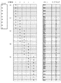
印刷された成果は、「パターン」と標示された列に示されている。いかなるサブピクセル行も欠けることなくパターンが完全であることがわかる。したがって、使用可能なデバイス部域は、サブピクセル行1からサブピクセル行24までである。
The printed results are shown in the column labeled “Pattern”. It can be seen that the pattern is complete without missing any subpixel rows. Thus, the usable device area is from
図5では、3つの色、赤、青そして緑が存在する。プリントヘッド上には9本のノズルが存在し、ノズル間の間隔どりは、2サブピクセルピッチ単位である。したがってこの図中:
c=3、
z=9、
p=2(s)および
n1=3である。
In FIG. 5, there are three colors, red, blue and green. There are nine nozzles on the print head, and the spacing between the nozzles is in units of 2 subpixel pitches. So in this figure:
c = 3,
z = 9,
p = 2 (s) and n 1 = 3.
色は、「プリンタ」列内に示されている通りに配列される。プリントヘッドは、加工物の第1の縁部で、サブピクセル行1の上のA1に位置づけされる。プリンタは行方向に加工物を横断して印刷し、サブピクセル行1に赤の行を形成し、サブピクセル行3に緑の行を、サブピクセル行5に青の行を、サブピクセル行7に赤の行を、サブピクセル行9に緑の行を、サブピクセル行11に青の行を、サブピクセル行13に赤の行を、サブピクセル行15に緑の行を、そしてサブピクセル行17に青の行を形成する。これは、印刷番号1と標示された列内に示されている。図3の場合と同様、明確さを期して各色について1つのサブピクセルのみが示されているが、各々全てのサブピクセル行を表わしている。次にプリンタは、zサブピクセル単位である距離d1だけ横方向にシフトする。この場合、z=9である。これはプリンタに関して配置A2である。プリンタは次に第2の行セット、すなわちサブピクセル行10、16および22に赤の行を、サブピクセル行12,18および24に緑の行をそしてサブピクセル行14、20および26に青の行を印刷する。これは印刷番号2の列内に示されている。印刷番号2は、明確さを期して、印刷番号1の右へシフトされた状態で示されている。印刷番号1および印刷番号2の両方ならびに他の全てのPrint番号は、加工物を横断して印刷された全サブピクセル行を表わす。プリンタは次に印刷番号3については9サブピクセル単位シフトされ、印刷番号4についてはさらに9サブピクセル単位シフトされ、印刷番号5についてはさらに9サブピクセル単位シフトされる。
The colors are arranged as shown in the “Printer” column. The printhead is positioned at A1 above
この時点でプリンタは、9サブピクセル行を5セット、つまり45サブピクセル行を印刷し終えている。印刷された成果は、「パターン」と標示された列に示されている。第1の縁部ではサブピクセル行2、4、6および8について、反対の縁部ではサブピクセル行46、48、50および52についてサブピクセルが欠けていることがわかる。3色が完全なセットひいては使用可能なデバイス部域は、サブピクセル行9からサブピクセル行44までに見出すことができる。この図では赤、青および緑が例示されているが、その他の色も使用できると考えられる。
At this point, the printer has finished printing 5 sets of 9 subpixel rows,
図6では、4種類の色M1、M2、M3およびM4が存在する。プリントヘッド上には8本のノズルが存在し、ノズル間の間隔どりは、3サブピクセルピッチ単位である。したがってこの図中:
c=4、
z=8、
p=3(s)および
n1=2である。
In FIG. 6, there are four types of colors M1, M2, M3 and M4. There are 8 nozzles on the print head, and the spacing between the nozzles is 3 subpixel pitch units. So in this figure:
c = 4,
z = 8,
p = 3 (s) and n 1 = 2.
色は、「プリンタ」の列内に示されている通りに配列される。プリントヘッドは、加工物の第1の縁部でサブピクセル行1より上のA1に位置づけされる。プリンタは行方向に加工物を横断して印刷し、サブピクセル行1にM1の行を形成し、サブピクセル行4にM2の行を、サブピクセル行7にM3の行を、サブピクセル行10にM4の行を、サブピクセル行13にM1の行を、サブピクセル行16にM2の行を、サブピクセル行19にM3の行をそしてサブピクセル行22にM4の行を形成する。これは、印刷番号1と標示された列内に示されている。図3の場合と同様、明確さを期して各色について1つのサブピクセルのみが示されているが、各々は全てのサブピクセル行を表わしている。次にプリンタは、zサブピクセル単位である距離d1だけ横方向にシフトする。この場合、z=8である。これはプリンタに関して配置A2である。プリンタは次に第2の行セット、すなわちサブピクセル行9および21にM1を、サブピクセル行12および24にM2を、サブピクセル行15および27にM3を、そしてサブピクセル行18および30にM4を印刷する。これは印刷番号2の列内に示されている。印刷番号2は、明確さを期して、印刷番号1の右へシフトされた状態で示されている。印刷番号1および印刷番号2の両方ならびに他の全ての印刷番号は、加工物を横断して印刷された全サブピクセル行を表わす。プリンタは次に印刷番号3については8サブピクセル単位シフトされ、印刷番号4についてはさらに8サブピクセル単位シフトされ、印刷番号5についてはさらに8サブピクセル単位シフトされる。
The colors are arranged as shown in the “Printer” column. The printhead is positioned at A1 above
この時点でプリンタは、8サブピクセル行を5セット、つまり40サブピクセル行を印刷し終えている。
At this point, the printer has finished printing 5 sets of 8 subpixel rows,
印刷された成果は、「パターン」と標示された列に示されている。第1の縁部ではサブピクセル行2、3、5、6、8、11および14について、反対の縁部ではサブピクセル行41、44、47、49、50、52および53についてサブピクセルが欠けていることがわかる。4色が完全なセットひいては使用可能なデバイス部域は、サブピクセル行15からサブピクセル行38までに見出すことができる。一例として4色システムは、赤、緑、青および白の色を使用する。所望される場合、その他の色セットを使用することもできる。
The printed results are shown in the column labeled “Pattern”. Missing subpixels for
一部の場合において、デバイスの全ての色が印刷されるわけではない。1つ以上の色を、他の堆積方法を用いて堆積させてもよい。このような方法には、蒸着、熱転写および連続液相成長技術、例えばスピンコーティング、グラビアコーティング、カーテンコーティング、ディップコーティング、スロットダイコーティングおよびスプレーコーティングが含まれるが、これらに限定されるわけではない。これらの場合において、印刷は、印刷ステップの前後に適用され得る印刷されていない色のための空間を残さなくてはならない。印刷パターンに関しては、空間が1つの色として計数される。 In some cases, not all colors of the device are printed. One or more colors may be deposited using other deposition methods. Such methods include, but are not limited to, vapor deposition, thermal transfer and continuous liquid phase growth techniques such as spin coating, gravure coating, curtain coating, dip coating, slot die coating and spray coating. In these cases, printing must leave space for unprinted colors that can be applied before and after the printing step. For the print pattern, the space is counted as one color.
この一例が図7に示されている。2つの色M1およびM2そして、異なる時点で堆積されるべき第3の色のための空間が存在し、この空間は図中で「空白」で示されている。これは3色として計数される。M1を印刷する3本のノズル、M2を印刷する3本のノズルそして印刷を行わない3本のノズルが存在する。非印刷ノズルは、プリントヘッド上に物理的に存在してもしなくてもよい。非印刷ノズルが存在しない場合、これらのための空間が存在し、この空間は、印刷パターンに関してはノズルとして計数される。したがって、これは合計9本のノズルとして計数される。各色に1種類ずつの異なる液体組成物と、空間のための1つの欠落が、規則的な交互パターンで供給される。ノズル(印刷ノズルと非印刷ノズル)の間の間隔どりは、2サブピクセルピッチ単位である。
したがってこの図中:
c=3、
z=9、
p=(c−1)s=2s、および
n1=3である。
An example of this is shown in FIG. There is a space for the two colors M1 and M2 and a third color to be deposited at different times, this space being indicated by “blank” in the figure. This is counted as three colors. There are three nozzles that print M1, three nozzles that print M2, and three nozzles that do not print. Non-printing nozzles may or may not be physically present on the printhead. If there are no non-printing nozzles, there is a space for them, which is counted as a nozzle with respect to the print pattern. Therefore, this counts as a total of 9 nozzles. One different liquid composition for each color and one drop for space are provided in a regular alternating pattern. The spacing between the nozzles (printing nozzles and non-printing nozzles) is 2 subpixel pitch units.
So in this figure:
c = 3,
z = 9,
p = (c−1) s = 2s, and n 1 = 3.
色は、「プリンタ」列内に示されている通りに配列され、ここで「空白」は非印刷ノズルを表わす。プリントヘッドは、加工物の第1の縁部で、サブピクセル行1の上のA1に位置づけされる。プリンタは行方向に加工物を横断して印刷し、サブピクセル行1、7および13にM1色の行を形成し、サブピクセル行3、9および15にM2色の行を形成する。これは、印刷番号1と標示された列内に示されている。図3の場合と同様、明確さを期して各色について1つのサブピクセルのみが示されているが、各々は1つのサブピクセル行全体を表わしている。次にプリンタは、9サブピクセル単位である距離d1=zだけ横方向にシフトする。これはプリンタに関して配置A2である。プリンタは次に第2の行セット、すなわちサブピクセル行10、16および22にM1色の行を、そしてサブピクセル行12、18および24にM2色の行を印刷する。これは印刷番号2の列内に示されている。印刷番号2は、明確さを期して、印刷番号1の右へシフトされた状態で示されている。印刷番号1および印刷番号2の両方ならびに他の全ての印刷番号は、加工物を横断して印刷された全サブピクセル行を表わす。プリンタは次に印刷番号3については9サブピクセル単位シフトされ、印刷番号4についてはさらに9サブピクセル単位シフトされ、印刷番号5についてはさらに9サブピクセル単位シフトされる。
The colors are arranged as shown in the “Printer” column, where “blank” represents a non-printing nozzle. The printhead is positioned at A1 above
この時点でプリンタは、非印刷ノズルからの行を含めて9サブピクセル行のセットを5セット、つまり45行を印刷し終えている。 At this point, the printer has finished printing 5 sets of 9 subpixel rows including the rows from the non-printing nozzles, that is, 45 rows.
印刷された成果は、「パターン」と標示された列に示されている。縁部ではサブピクセル行5、8、11など、第3の色のために利用可能である開放サブピクセルが非印刷行内に存在していることがわかる。2色が完全なセットに第3の色のための空欄を加えたものひいては使用可能なデバイス部域はサブピクセル行7からサブピクセル行45までに見出すことができる。一部の実施形態において、印刷された色は赤と緑であり、青は別途追加される。その他の色組合せも使用可能である。
The printed results are shown in the column labeled “Pattern”. It can be seen that there are open subpixels in the non-printed rows that are available for the third color, such as
4.電子デバイス
本明細書中で記述されている印刷方法を使用できるデバイスには、有機電子デバイスが含まれる。「有機電子デバイス」または時として単に「電子デバイス」という用語は、1つ以上の有機半導体層または材料を含むデバイスを意味するように意図されている。有機電子デバイスとしては、(1)電気エネルギーを放射線に変換するデバイス(例えば発光ダイオード、発光ダイオードディスプレイ、ダイオードレーザーまたは照明パネル)、(2)電子的プロセスを用いて信号を検出するデバイス(例えば光検出器、光伝導セル、フォトレジスター、フォトスイッチ、フォトトランジスタ、光電管、赤外線(「IR」)検出器またはバイオセンサー)、(3)放射線を電気エネルギーに変換するデバイス(例えば光起電装置または太陽電池)、(4)1つ以上の有機半導体層を含む1つ以上の電子部品を含むデバイス(例えばトランジスタまたはダイオード)、または項目(1)〜(4)中のデバイスの任意の組合せが含まれるがこれらに限定されない。
4). Electronic devices Devices that can use the printing methods described herein include organic electronic devices. The term “organic electronic device” or sometimes simply “electronic device” is intended to mean a device comprising one or more organic semiconductor layers or materials. Organic electronic devices include: (1) devices that convert electrical energy into radiation (eg, light emitting diodes, light emitting diode displays, diode lasers or lighting panels); (2) devices that detect signals using electronic processes (eg, light Detectors, photoconductive cells, photoresistors, photoswitches, phototransistors, phototubes, infrared (“IR”) detectors or biosensors), (3) devices that convert radiation into electrical energy (eg, photovoltaic or solar) Battery), (4) a device including one or more electronic components including one or more organic semiconductor layers (eg, transistors or diodes), or any combination of devices in items (1)-(4) However, it is not limited to these.
このようなデバイスにおいては、2つの電気接点層の間に有機活性層が挟まれている。電気接点層の少なくとも1つは光透過性であり、したがって光は電気接点層を通過できる。有機活性層は、電気接点層を横断して電気を印加した時点で、光透過性電気接点層を通って発光する。発光層と電気接点層の間に、追加の電気活性層が存在してもよい。 In such devices, an organic active layer is sandwiched between two electrical contact layers. At least one of the electrical contact layers is light transmissive, so that light can pass through the electrical contact layer. The organic active layer emits light through the light transmissive electrical contact layer when electricity is applied across the electrical contact layer. There may be an additional electroactive layer between the light emitting layer and the electrical contact layer.
必要な色を提供するためにこのようなデバイス内で活性成分として有機電界発光化合物を使用することは周知である。本明細書中に記述されている印刷方法は、異なる色を有する電界発光材料を含む液体組成物の印刷向けに適している。このような材料としては、小分子有機蛍光化合物、蛍光および燐光性金属錯体、共役ポリマーおよびそれらの混合物が含まれるがこれらに限定されない。蛍光化合物の例としてはクリセン類、ピレン類、ペリレン類、ルブレン類、クマリン類、アントラセン類、チアジアゾール類、その誘導体およびその混合物が含まれるがこれらに限定されない。金属錯体の例としては、金属キレート化オキシノイド化合物、例えばトリス(8−ヒドロキシキノラト)アルミニウム(Alq3);シクロメタレート化イリジウムおよび白金電界発光化合物、例えばPetrovらの米国特許第6,670,645号明細書および公開PCT出願国際公開第03/063555号パンフレットおよび国際公開第2004/016710号パンフレット中に開示されているフェニルピリジン、フェニルキノリンまたはフェニルピリミジンリガンドとイリジウムの錯体および例えば公開PCT出願国際公開第03/008424号パンフレット、国際公開第03/091688号パンフレットおよび国際公開第03/040257号パンフレット中に記載されている有機金属錯体およびそれらの混合物が含まれるがこれらに限定されない。一部の場合において、小分子蛍光または有機金属材料は、加工および/または電子特性を改善するためにホスト材料と共にドーパントとして堆積させられる。共役ポリマーの例としては、ポリ(フェニレンビニレン類)、ポリフルオレン類、ポリ(スピロビフルオレン類)、ポリチオフェン類、ポリ(p−フェニレン類)、そのコポリマーおよびその混合物が含まれるがこれらに限定されない。 It is well known to use organic electroluminescent compounds as active ingredients in such devices to provide the required color. The printing methods described herein are suitable for printing liquid compositions comprising electroluminescent materials having different colors. Such materials include, but are not limited to, small molecule organic fluorescent compounds, fluorescent and phosphorescent metal complexes, conjugated polymers, and mixtures thereof. Examples of fluorescent compounds include, but are not limited to, chrysenes, pyrenes, perylenes, rubrenes, coumarins, anthracenes, thiadiazoles, derivatives thereof and mixtures thereof. Examples of metal complexes include metal chelated oxinoid compounds such as tris (8-hydroxyquinolato) aluminum (Alq3); iridium cyclometallated and platinum electroluminescent compounds such as US Pat. No. 6,670,645 to Petrov et al. And iridium complexes of phenylpyridine, phenylquinoline or phenylpyrimidine ligands disclosed in WO 03/063555 and WO 2004/016710, and published PCT applications. Included are organometallic complexes and mixtures thereof described in pamphlet No. 03/008424, pamphlet of WO 03/091688 and pamphlet of WO 03/040257. But not limited to these. In some cases, small molecule fluorescent or organometallic materials are deposited as dopants with the host material to improve processing and / or electronic properties. Examples of conjugated polymers include, but are not limited to, poly (phenylene vinylenes), polyfluorenes, poly (spirobifluorenes), polythiophenes, poly (p-phenylenes), copolymers thereof and mixtures thereof. .
印刷用インクを形成するためには、上述の材料は、適切な液体組成物の中に溶解されるかまたは分散される。特定の化合物または関連する化合物部類のための適切な溶媒は、当業者が容易に決定できる。一部の利用分野のためには、化合物を非水性溶媒中に溶解させることが望ましい。このような非水性溶媒は比較的極性のもの、例えばC1〜C20アルコール、エーテルおよび酸性エステルであり得、または比較的非極性のもの、例えばC1〜C12アルカンまたは芳香族、例えばトルエン、キシレン類、トリフルオロトルエンなどであり得る。新規化合物を含む本明細書に記述されている通りの溶液または分散のいずれかとしての液体組成物を製造する上で使用するためのその他の適切な液体としては、塩素化炭化水素(例えば塩化メチレン、クロロホルム、クロロベンゼン)、芳香族炭化水素(たとえばトリフルオロトルエンを含む置換および未置換トルエンおよびキシレン類)、極性溶媒(例えばテトラヒドロフラン(THP)、N−メチルピロリドン)、エステル類(たとえば酢酸エチル)、アルコール類(イソプロパノール)、ケトン(keytones)類(シクロペンタトン)およびその混合物が含まれるがこれらに限定されない。光活性材料用の適切な溶媒は、例えば公開PCT出願国際公開第2007/145979号パンフレット中に記載されている。 To form a printing ink, the materials described above are dissolved or dispersed in a suitable liquid composition. Appropriate solvents for a particular compound or related compound class can be readily determined by one skilled in the art. For some applications, it is desirable to dissolve the compound in a non-aqueous solvent. Such non-aqueous solvents are relatively polar ones, for example, C 1 -C 20 alcohol, to give an ether and acid esters, or relatively non-polar ones, for example, C 1 -C 12 alkane or aromatic, such as toluene , Xylenes, trifluorotoluene and the like. Other suitable liquids for use in preparing liquid compositions as either solutions or dispersions as described herein containing the novel compound include chlorinated hydrocarbons (eg, methylene chloride). , Chloroform, chlorobenzene), aromatic hydrocarbons (eg substituted and unsubstituted toluene and xylenes including trifluorotoluene), polar solvents (eg tetrahydrofuran (THP), N-methylpyrrolidone), esters (eg ethyl acetate), Examples include, but are not limited to, alcohols (isopropanol), ketones (cyclopentatone), and mixtures thereof. Suitable solvents for the photoactive material are described, for example, in published PCT application WO 2007/1457979.
有機電子デバイス構造の一例はOLEDである。デバイスは、アノード層である第1の電気接点層と、カソード層160である第2の電気接点層を有する。光活性層はこれらの間にある。場合により、追加の層が存在してもよい。アノードに隣接して、緩衝層があってもよい。緩衝層に隣接して正孔輸送材料を含む正孔輸送層があってもよい。カソードに隣接して、電子輸送材料を含む電子輸送層があってもよい。一つの選択肢として、デバイスは、アノードに隣接して1つ以上の追加の正孔注入または正孔輸送層、および/またはカソードに隣接して1つ以上の追加の電子注入または電子輸送層を使用してもよい。 An example of an organic electronic device structure is an OLED. The device has a first electrical contact layer that is an anode layer and a second electrical contact layer that is a cathode layer 160. The photoactive layer is between them. In some cases, additional layers may be present. There may be a buffer layer adjacent to the anode. There may be a hole transport layer comprising a hole transport material adjacent to the buffer layer. There may be an electron transport layer comprising an electron transport material adjacent to the cathode. As one option, the device uses one or more additional hole injection or hole transport layers adjacent to the anode and / or one or more additional electron injection or electron transport layers adjacent to the cathode. May be.
一般的記述または実施例において上述した活動の全てが必要とされるわけではないこと、特定の活動の一部分が不要な場合があること、そして記述されているものに加えて1つ以上のさらなる活動が実施される場合があることに留意されたい。さらにまた活動が列挙されている順序は必ずしもそれらが実施される順序ではない。 That not all of the activities described above in the general description or examples are required, that some of the specific activities may be unnecessary, and one or more additional activities in addition to those described Note that may be implemented. Furthermore, the order in which activities are listed is not necessarily the order in which they are performed.
以上の明細書において、具体的実施形態を基準として概念を記述してきた。しかしながら、当業者であれば、以下のクレーム中で記されている本発明の範囲から逸脱することなくさまざまな修正および変更を加えることができるということがわかる。したがって、本明細書および図面は、限定的な意味合いでではなく例示的な意味で考慮されるべきものであり、このような修正は全て本発明の範囲内に含まれるように意図されている。 In the above specification, the concept has been described based on specific embodiments. However, one of ordinary skill in the art appreciates that various modifications and changes can be made without departing from the scope of the present invention as set forth in the claims below. The specification and drawings are, accordingly, to be regarded in an illustrative sense rather than a restrictive sense, and all such modifications are intended to be included within the scope of the present invention.
具体的実施形態に関して、利益、その他の利点および課題に対する解決法を、以上で記述してきた。しかしながら、利益、利点、課題に対する解決法ならびに、いずれかの利益、利点または解決法を発生させるまたはより顕著にさせることがあるあらゆる特徴を、いずれかのまたは全てのクレームの非常に重要な、所要のまたは不可欠の特徴とみなすべきではない。 With respect to specific embodiments, benefits, other advantages and solutions to problems have been described above. However, benefits, benefits, solutions to problems, and any features that may generate or make any benefit, advantage or solution a very important requirement of any or all claims It should not be considered an essential or essential feature.
本明細書中において、明確さを期して別個の実施形態に関連して記述されている一部の特徴を、単一の実施形態の中に組合せた形で提供してもよい、ということを認識すべきである。反対に、簡略化のため単一の実施形態に関連して記述されているさまざまな特徴を、別個に、または任意の下位組合せの形で提供してもよい。本明細書中で規定されているさまざまな範囲内の数値の使用は、あたかもその提示された範囲内の最小値および最大値の両方の前に「約」という語があるかのように、近似値として提示されてもよい。このようにして、提示された範囲の上下のわずかな変形形態を用いて、範囲内の値と実質的に同じ結果を達成することができる。同様に、これらの範囲の開示は、1つの値の一部の成分を異なる値の一部の成分と混合した場合に結果としてもたらされ得る少数値を含めた最小および最大平均値の間の全ての値を含む連続的範囲として意図されている。さらに、より広い範囲およびより狭い範囲が開示されている場合、1つの範囲からの最小値を、別の範囲からの最大値と整合させることおよびその逆が、本発明が企図するものの中に入る。
なお、本発明は、特許請求の範囲を含め、以下の発明を包含する。
1.加工物上に規則的アレイをサブピクセル行印刷する方法において、前記サブピクセルがc種類の異なる色を有しかつサブピクセルピッチsを有する方法であって、
(a) pというノズル間間隔を伴って行の形で配置されたz個のノズルを有するプリントヘッドを提供するステップであって、z=n1(c)、p=(c−1)(s)であり、前記プリントヘッドが前記加工物に対して第1の位置にあるステップと;
(b) 前記c種類の色の各々について1つずつのc種類の異なる印刷用インクを提供するステップと;
(c) 規則的な交互パターンで前記ノズルに前記印刷用インクの各々を供給するステップと;
(d) 前記プリントヘッドでz行のサブピクセルの第1のセットを印刷するステップと;
(e) 前記プリントヘッドに対して横方向に前記加工物を距離d1だけ移動させるステップであって、d1=z(s)であるステップと;
(f) 前記プリントヘッドでz行のサブピクセルの第2のセットを印刷するステップと;
(g) z行のサブピクセルを合計で(n2+2)セットのために、(e)ステップおよび(f)ステップをn2回反復するステップと、
を含み、
cは、1より大きい整数であり;
n1は、cが奇数である場合にはn1も奇数であることを条件として、0より大きい整数であり;
n2は0よりも大きい整数である、
方法。
2.cが2、3または4である、1に記載の方法。
3.n1が少なくとも2である、1に記載の方法。
4.c=2であり、かつn1=4〜8、n2=3である、1に記載の方法。
5.c=3であり、かつn1=3または5である、1に記載の方法。
6.c=4であり、n1=2〜4である、1に記載の方法。
7.各々の印刷用インクが電界発光材料と液体媒質を含む、1に記載の方法。
It is understood that some features described herein with reference to separate embodiments for clarity may be provided in combination in a single embodiment. Should be recognized. Conversely, various features that are described in the context of a single embodiment for simplicity may be provided separately or in any subcombination. The use of numerical values within the various ranges specified herein is an approximation as if the word “about” precedes both the minimum and maximum values within the stated range. It may be presented as a value. In this way, substantially the same results as values within the range can be achieved using slight variations above and below the presented range. Similarly, the disclosure of these ranges is between minimum and maximum average values, including decimal values that can result when some components of one value are mixed with some components of different values. It is intended as a continuous range that includes all values. Further, where a wider range and a narrower range are disclosed, matching the minimum value from one range to the maximum value from another range and vice versa is within the contemplation of the present invention. .
In addition, this invention includes the following invention including a claim.
1. A method of printing a regular array of subpixel rows on a workpiece, wherein the subpixels have c different colors and have a subpixel pitch s,
(A) providing a printhead having z nozzles arranged in rows with an inter-nozzle spacing of p, where z = n 1 (c), p = (c−1) ( s) and the print head is in a first position relative to the workpiece;
(B) providing c different printing inks, one for each of the c colors;
(C) supplying each of the printing inks to the nozzles in a regular alternating pattern;
(D) printing a first set of z rows of sub-pixels with the printhead;
(E) moving the workpiece laterally relative to the print head by a distance d 1 , where d 1 = z (s);
(F) printing a second set of z rows of sub-pixels with the printhead;
(G) repeating the steps (e) and (f) n 2 times for a total of (n 2 +2) sets of z rows of subpixels;
Including
c is an integer greater than 1;
n 1 is an integer greater than 0, provided that if c is odd, n 1 is also odd;
n 2 is an integer greater than 0,
Method.
2. 2. The method according to 1, wherein c is 2, 3 or 4.
3. The method of 1, wherein n 1 is at least 2.
4). The method according to 1, wherein c = 2, n 1 = 4 to 8, and n 2 = 3.
5. The method of 1, wherein c = 3 and n 1 = 3 or 5.
6). The method according to 1 , wherein c = 4 and n 1 = 2-4.
7). The method of 1, wherein each printing ink comprises an electroluminescent material and a liquid medium.
Claims (7)
(a) pというノズル間間隔を伴って一列に並んで配置されたz個のノズルを有するプリントヘッドを提供するステップであって、z=n1(c)、p=(c−1)(s)であり、前記プリントヘッドが前記加工物に対して第1の位置にあるステップと;
(b) 前記c種類の色の各々について1つずつのc種類の異なる印刷用インクを提供するステップと;
(c) 規則的な交互パターンで前記ノズルに前記印刷用インクの各々を供給するステップと;
(d) 前記プリントヘッドでz行のサブピクセルの第1のセットを印刷するステップと;
(e) 前記プリントヘッドの側面方向に対して前記加工物を距離d1だけ移動させるステップであって、d1=z(s)であるステップと;
(f) 前記プリントヘッドでz行のサブピクセルの第2のセットを印刷するステップと;
(g) z行のサブピクセルを合計で(n2+2)セットのために、(e)ステップおよび(f)ステップをn2回反復するステップと、
を含み、
cは、1より大きい整数であり;
n1は、cが奇数である場合にはn1も奇数であることを条件として、0より大きい整数であり;
n2は0よりも大きい整数である、
方法。 A method of printing a regular array of subpixel rows on a workpiece, wherein the subpixels have c different colors and have a subpixel pitch s,
(A) providing a print head having z nozzles arranged in a line with an inter-nozzle spacing of p, wherein z = n 1 (c), p = (c−1) ( s) and the print head is in a first position relative to the workpiece;
(B) providing c different printing inks, one for each of the c colors;
(C) supplying each of the printing inks to the nozzles in a regular alternating pattern;
(D) printing a first set of z rows of sub-pixels with the printhead;
(E) moving the workpiece by a distance d 1 with respect to the lateral direction of the print head , wherein d 1 = z (s);
(F) printing a second set of z rows of sub-pixels with the printhead;
(G) repeating the steps (e) and (f) n 2 times for a total of (n 2 +2) sets of z rows of subpixels;
Including
c is an integer greater than 1;
n 1 is an integer greater than 0, provided that if c is odd, n 1 is also odd;
n 2 is an integer greater than 0,
Method.
Applications Claiming Priority (3)
| Application Number | Priority Date | Filing Date | Title |
|---|---|---|---|
| US15801709P | 2009-03-06 | 2009-03-06 | |
| US61/158,017 | 2009-03-06 | ||
| PCT/US2010/026469 WO2010102274A2 (en) | 2009-03-06 | 2010-03-08 | Multicolor electronic devices and processes of forming the same by printing |
Publications (3)
| Publication Number | Publication Date |
|---|---|
| JP2012519942A JP2012519942A (en) | 2012-08-30 |
| JP2012519942A5 JP2012519942A5 (en) | 2013-04-25 |
| JP5612613B2 true JP5612613B2 (en) | 2014-10-22 |
Family
ID=42710247
Family Applications (1)
| Application Number | Title | Priority Date | Filing Date |
|---|---|---|---|
| JP2011553162A Expired - Fee Related JP5612613B2 (en) | 2009-03-06 | 2010-03-08 | Multicolor electronic device and method for forming it by printing |
Country Status (6)
| Country | Link |
|---|---|
| US (1) | US8459776B2 (en) |
| EP (1) | EP2404213A2 (en) |
| JP (1) | JP5612613B2 (en) |
| KR (1) | KR20110127735A (en) |
| CN (1) | CN102341747B (en) |
| WO (1) | WO2010102274A2 (en) |
Families Citing this family (6)
| Publication number | Priority date | Publication date | Assignee | Title |
|---|---|---|---|---|
| KR20100106470A (en) | 2007-12-10 | 2010-10-01 | 이 아이 듀폰 디 네모아 앤드 캄파니 | Multicolor electronic devices and processes of forming the same by printing |
| US8675252B2 (en) * | 2008-10-21 | 2014-03-18 | E. I. Du Pont De Nemours And Company | Multicolor electronic devices and processes of forming the same by printing |
| KR20110127735A (en) | 2009-03-06 | 2011-11-25 | 이 아이 듀폰 디 네모아 앤드 캄파니 | Multicolor electronic devices and processes of forming the same by printing |
| CN102449805B (en) * | 2009-06-04 | 2015-06-10 | E.I.内穆尔杜邦公司 | Multicolor electronic devices and processes of forming the same by printing |
| WO2010141699A2 (en) * | 2009-06-04 | 2010-12-09 | E. I. Du Pont De Nemours And Company | Multicolor electronic devices and processes of forming the same by printing |
| KR102642502B1 (en) * | 2018-11-07 | 2024-03-04 | 삼성디스플레이 주식회사 | Inkjet printer apparatus and method of manufacturing driving the same |
Family Cites Families (32)
| Publication number | Priority date | Publication date | Assignee | Title |
|---|---|---|---|---|
| US5592202A (en) | 1994-11-10 | 1997-01-07 | Laser Master Corporation | Ink jet print head rail assembly |
| JPH08300694A (en) | 1995-05-11 | 1996-11-19 | Seiko Epson Corp | Color printer |
| JP3111024B2 (en) | 1995-07-19 | 2000-11-20 | キヤノン株式会社 | Apparatus and method for manufacturing color filter, method for manufacturing display apparatus, and method for manufacturing apparatus provided with display apparatus |
| JPH1148503A (en) | 1997-08-05 | 1999-02-23 | Seiko Epson Corp | Ink-jet recording head and ink-jet recording apparatus |
| TW471011B (en) * | 1999-10-13 | 2002-01-01 | Semiconductor Energy Lab | Thin film forming apparatus |
| US6670645B2 (en) | 2000-06-30 | 2003-12-30 | E. I. Du Pont De Nemours And Company | Electroluminescent iridium compounds with fluorinated phenylpyridines, phenylpyrimidines, and phenylquinolines and devices made with such compounds |
| US6655783B2 (en) * | 2001-05-23 | 2003-12-02 | Seiko Epson Corporation | Printing by switching sub-scanning feed between monochromatic areas and color areas |
| JP2003010764A (en) * | 2001-06-29 | 2003-01-14 | Dainippon Screen Mfg Co Ltd | Substrate coating apparatus |
| US6875523B2 (en) | 2001-07-05 | 2005-04-05 | E. I. Du Pont De Nemours And Company | Photoactive lanthanide complexes with phosphine oxides, phosphine oxide-sulfides, pyridine N-oxides, and phosphine oxide-pyridine N-oxides, and devices made with such complexes |
| US6924047B2 (en) | 2001-07-18 | 2005-08-02 | E.I. Du Pont De Nemours And Company | Luminescent lanthanide complexes with imine ligands and devices made with such complexes |
| JP3958014B2 (en) | 2001-10-12 | 2007-08-15 | 富士フイルム株式会社 | Pattern sheet manufacturing method and manufacturing apparatus |
| US7166368B2 (en) | 2001-11-07 | 2007-01-23 | E. I. Du Pont De Nemours And Company | Electroluminescent platinum compounds and devices made with such compounds |
| EP2299785A1 (en) | 2001-12-26 | 2011-03-23 | E. I. du Pont de Nemours and Company | Iridium compounds |
| US6963005B2 (en) | 2002-08-15 | 2005-11-08 | E. I. Du Pont De Nemours And Company | Compounds comprising phosphorus-containing metal complexes |
| JP2004358314A (en) * | 2003-06-03 | 2004-12-24 | Seiko Epson Corp | Liquid drop delivery method, liquid drop delivery device, method for manufacturing device, apparatus for manufacturing device and electronic instrument |
| JP2005087801A (en) * | 2003-09-12 | 2005-04-07 | Seiko Epson Corp | Plotting method, plotting device and electro-optical device |
| JP4407225B2 (en) | 2003-10-07 | 2010-02-03 | セイコーエプソン株式会社 | Drawing method |
| KR100603837B1 (en) | 2004-12-09 | 2006-07-24 | 엘지.필립스 엘시디 주식회사 | Color filter substrate for liquid crystal display device and method of fabricating the same |
| JP2006341406A (en) | 2005-06-07 | 2006-12-21 | Canon Inc | Inkjet recording system |
| KR100727942B1 (en) | 2005-06-25 | 2007-06-13 | 삼성전자주식회사 | Ink-jet image forming apparatus and method for printing high resolution |
| KR20070073158A (en) | 2006-01-04 | 2007-07-10 | 삼성전자주식회사 | Ink jet printing system and manufacturing method of display using the same |
| KR100756581B1 (en) | 2006-02-15 | 2007-09-10 | 삼성전자주식회사 | Apparatus and method for manufacturing display device |
| JP2007256312A (en) * | 2006-03-20 | 2007-10-04 | Toppan Printing Co Ltd | Manufacturing method for color filter, manufacturing method for organic electroluminescence element, and ink jet coating device used therefor |
| KR100759838B1 (en) | 2006-05-08 | 2007-09-18 | (주)에스티아이 | Method for patterning color filter of liquid crystal display using ink-jet |
| WO2007145975A2 (en) | 2006-06-05 | 2007-12-21 | E. I. Du Pont De Nemours And Company | Process for forming an organic light-emitting diode and devices made by the process |
| US20080067473A1 (en) | 2006-06-05 | 2008-03-20 | Walker Dennis D | Liquid composition for deposition of organic active materials |
| US20080157659A1 (en) | 2006-12-28 | 2008-07-03 | Shiva Prakash | Electronic device including an organic device layer |
| JP2008197149A (en) * | 2007-02-08 | 2008-08-28 | Nsk Ltd | Method for producing color filter, and exposure apparatus for producing color filter |
| US8675252B2 (en) | 2008-10-21 | 2014-03-18 | E. I. Du Pont De Nemours And Company | Multicolor electronic devices and processes of forming the same by printing |
| KR20110127735A (en) | 2009-03-06 | 2011-11-25 | 이 아이 듀폰 디 네모아 앤드 캄파니 | Multicolor electronic devices and processes of forming the same by printing |
| WO2010141699A2 (en) | 2009-06-04 | 2010-12-09 | E. I. Du Pont De Nemours And Company | Multicolor electronic devices and processes of forming the same by printing |
| CN102449805B (en) | 2009-06-04 | 2015-06-10 | E.I.内穆尔杜邦公司 | Multicolor electronic devices and processes of forming the same by printing |
-
2010
- 2010-03-08 KR KR1020117023392A patent/KR20110127735A/en active Search and Examination
- 2010-03-08 WO PCT/US2010/026469 patent/WO2010102274A2/en active Application Filing
- 2010-03-08 EP EP10749430A patent/EP2404213A2/en not_active Withdrawn
- 2010-03-08 US US13/202,235 patent/US8459776B2/en active Active
- 2010-03-08 CN CN201080011411.0A patent/CN102341747B/en not_active Expired - Fee Related
- 2010-03-08 JP JP2011553162A patent/JP5612613B2/en not_active Expired - Fee Related
Also Published As
| Publication number | Publication date |
|---|---|
| US8459776B2 (en) | 2013-06-11 |
| CN102341747B (en) | 2014-04-30 |
| US20110298863A1 (en) | 2011-12-08 |
| WO2010102274A3 (en) | 2011-01-13 |
| EP2404213A2 (en) | 2012-01-11 |
| CN102341747A (en) | 2012-02-01 |
| WO2010102274A2 (en) | 2010-09-10 |
| JP2012519942A (en) | 2012-08-30 |
| KR20110127735A (en) | 2011-11-25 |
Similar Documents
| Publication | Publication Date | Title |
|---|---|---|
| JP5411283B2 (en) | Multicolor electronic device and method for forming the same by printing | |
| US9011967B2 (en) | Multicolor electronic devices and processes of forming the same by printing | |
| JP5612613B2 (en) | Multicolor electronic device and method for forming it by printing | |
| US8616666B2 (en) | Multicolor electronic devices and processes of forming the same by printing | |
| JP5576482B2 (en) | Multi-color electronic device and method for forming multi-color electronic device by printing | |
| US8574934B2 (en) | OVJP patterning of electronic devices | |
| US8154700B2 (en) | Electronic device having electrodes and organic active regions and processes of forming the same | |
| US7050697B1 (en) | Pixel arrangement for organic electronic devices | |
| US9662918B2 (en) | Gradient ink containment printing process and apparatus |
Legal Events
| Date | Code | Title | Description |
|---|---|---|---|
| A521 | Request for written amendment filed |
Free format text: JAPANESE INTERMEDIATE CODE: A523 Effective date: 20130304 |
|
| A621 | Written request for application examination |
Free format text: JAPANESE INTERMEDIATE CODE: A621 Effective date: 20130304 |
|
| A977 | Report on retrieval |
Free format text: JAPANESE INTERMEDIATE CODE: A971007 Effective date: 20131016 |
|
| A131 | Notification of reasons for refusal |
Free format text: JAPANESE INTERMEDIATE CODE: A131 Effective date: 20131022 |
|
| A521 | Request for written amendment filed |
Free format text: JAPANESE INTERMEDIATE CODE: A523 Effective date: 20140121 |
|
| TRDD | Decision of grant or rejection written | ||
| A01 | Written decision to grant a patent or to grant a registration (utility model) |
Free format text: JAPANESE INTERMEDIATE CODE: A01 Effective date: 20140805 |
|
| A61 | First payment of annual fees (during grant procedure) |
Free format text: JAPANESE INTERMEDIATE CODE: A61 Effective date: 20140904 |
|
| R150 | Certificate of patent or registration of utility model |
Ref document number: 5612613 Country of ref document: JP Free format text: JAPANESE INTERMEDIATE CODE: R150 |
|
| LAPS | Cancellation because of no payment of annual fees |