JP5606908B2 - Method for producing a fine conductive structure on a surface - Google Patents
Method for producing a fine conductive structure on a surface Download PDFInfo
- Publication number
- JP5606908B2 JP5606908B2 JP2010516400A JP2010516400A JP5606908B2 JP 5606908 B2 JP5606908 B2 JP 5606908B2 JP 2010516400 A JP2010516400 A JP 2010516400A JP 2010516400 A JP2010516400 A JP 2010516400A JP 5606908 B2 JP5606908 B2 JP 5606908B2
- Authority
- JP
- Japan
- Prior art keywords
- substrate
- ink
- channel
- conductive
- conductive structure
- Prior art date
- Legal status (The legal status is an assumption and is not a legal conclusion. Google has not performed a legal analysis and makes no representation as to the accuracy of the status listed.)
- Expired - Fee Related
Links
Images


Classifications
-
- H—ELECTRICITY
- H05—ELECTRIC TECHNIQUES NOT OTHERWISE PROVIDED FOR
- H05K—PRINTED CIRCUITS; CASINGS OR CONSTRUCTIONAL DETAILS OF ELECTRIC APPARATUS; MANUFACTURE OF ASSEMBLAGES OF ELECTRICAL COMPONENTS
- H05K3/00—Apparatus or processes for manufacturing printed circuits
- H05K3/10—Apparatus or processes for manufacturing printed circuits in which conductive material is applied to the insulating support in such a manner as to form the desired conductive pattern
- H05K3/12—Apparatus or processes for manufacturing printed circuits in which conductive material is applied to the insulating support in such a manner as to form the desired conductive pattern using thick film techniques, e.g. printing techniques to apply the conductive material or similar techniques for applying conductive paste or ink patterns
- H05K3/1258—Apparatus or processes for manufacturing printed circuits in which conductive material is applied to the insulating support in such a manner as to form the desired conductive pattern using thick film techniques, e.g. printing techniques to apply the conductive material or similar techniques for applying conductive paste or ink patterns by using a substrate provided with a shape pattern, e.g. grooves, banks, resist pattern
-
- H—ELECTRICITY
- H01—ELECTRIC ELEMENTS
- H01L—SEMICONDUCTOR DEVICES NOT COVERED BY CLASS H10
- H01L21/00—Processes or apparatus adapted for the manufacture or treatment of semiconductor or solid state devices or of parts thereof
- H01L21/02—Manufacture or treatment of semiconductor devices or of parts thereof
- H01L21/027—Making masks on semiconductor bodies for further photolithographic processing not provided for in group H01L21/18 or H01L21/34
-
- H—ELECTRICITY
- H05—ELECTRIC TECHNIQUES NOT OTHERWISE PROVIDED FOR
- H05K—PRINTED CIRCUITS; CASINGS OR CONSTRUCTIONAL DETAILS OF ELECTRIC APPARATUS; MANUFACTURE OF ASSEMBLAGES OF ELECTRICAL COMPONENTS
- H05K3/00—Apparatus or processes for manufacturing printed circuits
- H05K3/0011—Working of insulating substrates or insulating layers
- H05K3/0014—Shaping of the substrate, e.g. by moulding
-
- H—ELECTRICITY
- H05—ELECTRIC TECHNIQUES NOT OTHERWISE PROVIDED FOR
- H05K—PRINTED CIRCUITS; CASINGS OR CONSTRUCTIONAL DETAILS OF ELECTRIC APPARATUS; MANUFACTURE OF ASSEMBLAGES OF ELECTRICAL COMPONENTS
- H05K3/00—Apparatus or processes for manufacturing printed circuits
- H05K3/10—Apparatus or processes for manufacturing printed circuits in which conductive material is applied to the insulating support in such a manner as to form the desired conductive pattern
- H05K3/107—Apparatus or processes for manufacturing printed circuits in which conductive material is applied to the insulating support in such a manner as to form the desired conductive pattern by filling grooves in the support with conductive material
-
- H—ELECTRICITY
- H05—ELECTRIC TECHNIQUES NOT OTHERWISE PROVIDED FOR
- H05K—PRINTED CIRCUITS; CASINGS OR CONSTRUCTIONAL DETAILS OF ELECTRIC APPARATUS; MANUFACTURE OF ASSEMBLAGES OF ELECTRICAL COMPONENTS
- H05K1/00—Printed circuits
- H05K1/02—Details
- H05K1/09—Use of materials for the conductive, e.g. metallic pattern
- H05K1/092—Dispersed materials, e.g. conductive pastes or inks
- H05K1/097—Inks comprising nanoparticles and specially adapted for being sintered at low temperature
-
- H—ELECTRICITY
- H05—ELECTRIC TECHNIQUES NOT OTHERWISE PROVIDED FOR
- H05K—PRINTED CIRCUITS; CASINGS OR CONSTRUCTIONAL DETAILS OF ELECTRIC APPARATUS; MANUFACTURE OF ASSEMBLAGES OF ELECTRICAL COMPONENTS
- H05K2201/00—Indexing scheme relating to printed circuits covered by H05K1/00
- H05K2201/01—Dielectrics
- H05K2201/0104—Properties and characteristics in general
- H05K2201/0108—Transparent
-
- H—ELECTRICITY
- H05—ELECTRIC TECHNIQUES NOT OTHERWISE PROVIDED FOR
- H05K—PRINTED CIRCUITS; CASINGS OR CONSTRUCTIONAL DETAILS OF ELECTRIC APPARATUS; MANUFACTURE OF ASSEMBLAGES OF ELECTRICAL COMPONENTS
- H05K2203/00—Indexing scheme relating to apparatus or processes for manufacturing printed circuits covered by H05K3/00
- H05K2203/01—Tools for processing; Objects used during processing
- H05K2203/0104—Tools for processing; Objects used during processing for patterning or coating
- H05K2203/0108—Male die used for patterning, punching or transferring
-
- H—ELECTRICITY
- H05—ELECTRIC TECHNIQUES NOT OTHERWISE PROVIDED FOR
- H05K—PRINTED CIRCUITS; CASINGS OR CONSTRUCTIONAL DETAILS OF ELECTRIC APPARATUS; MANUFACTURE OF ASSEMBLAGES OF ELECTRICAL COMPONENTS
- H05K2203/00—Indexing scheme relating to apparatus or processes for manufacturing printed circuits covered by H05K3/00
- H05K2203/01—Tools for processing; Objects used during processing
- H05K2203/0104—Tools for processing; Objects used during processing for patterning or coating
- H05K2203/013—Inkjet printing, e.g. for printing insulating material or resist
-
- H—ELECTRICITY
- H05—ELECTRIC TECHNIQUES NOT OTHERWISE PROVIDED FOR
- H05K—PRINTED CIRCUITS; CASINGS OR CONSTRUCTIONAL DETAILS OF ELECTRIC APPARATUS; MANUFACTURE OF ASSEMBLAGES OF ELECTRICAL COMPONENTS
- H05K3/00—Apparatus or processes for manufacturing printed circuits
- H05K3/10—Apparatus or processes for manufacturing printed circuits in which conductive material is applied to the insulating support in such a manner as to form the desired conductive pattern
- H05K3/12—Apparatus or processes for manufacturing printed circuits in which conductive material is applied to the insulating support in such a manner as to form the desired conductive pattern using thick film techniques, e.g. printing techniques to apply the conductive material or similar techniques for applying conductive paste or ink patterns
- H05K3/1241—Apparatus or processes for manufacturing printed circuits in which conductive material is applied to the insulating support in such a manner as to form the desired conductive pattern using thick film techniques, e.g. printing techniques to apply the conductive material or similar techniques for applying conductive paste or ink patterns by ink-jet printing or drawing by dispensing
- H05K3/125—Apparatus or processes for manufacturing printed circuits in which conductive material is applied to the insulating support in such a manner as to form the desired conductive pattern using thick film techniques, e.g. printing techniques to apply the conductive material or similar techniques for applying conductive paste or ink patterns by ink-jet printing or drawing by dispensing by ink-jet printing
-
- Y—GENERAL TAGGING OF NEW TECHNOLOGICAL DEVELOPMENTS; GENERAL TAGGING OF CROSS-SECTIONAL TECHNOLOGIES SPANNING OVER SEVERAL SECTIONS OF THE IPC; TECHNICAL SUBJECTS COVERED BY FORMER USPC CROSS-REFERENCE ART COLLECTIONS [XRACs] AND DIGESTS
- Y10—TECHNICAL SUBJECTS COVERED BY FORMER USPC
- Y10T—TECHNICAL SUBJECTS COVERED BY FORMER US CLASSIFICATION
- Y10T428/00—Stock material or miscellaneous articles
- Y10T428/26—Web or sheet containing structurally defined element or component, the element or component having a specified physical dimension
Description
本発明は、小さいミクロの伝導性構造体を表面に製造することを可能にする方法を開示する。本明細書中、小さいミクロの構造体は、通常、視覚補助具を用いた裸眼によってはじめて見られる構造体と理解される。これは、ナノスケールのくぼみの(ホット)スタンピングおよび/またはインプリンティングによってミクロチャネルを製造すること、次の、このようにして作り出されるくぼみへの毛細管現象の物理的効果に補助される伝導性材料の的を絞った導入、および最後に伝導性材料の好適な後処理によって達成される。 The present invention discloses a method that allows small micro conductive structures to be produced on a surface. In the present specification, a small micro structure is generally understood as a structure that is first seen by the naked eye using a visual aid. This is a conductive material that is assisted by the fabrication of microchannels by nanoscale indentation (hot) stamping and / or imprinting, followed by the physical effect of capillary action on the indentation thus created This is achieved by targeted introduction and finally by suitable post-treatment of the conductive material.
表面、特に非導電性であるかまたは導電性の低い透明物体の表面、に導電性構造体を付け、それによってそれらの光学的または機械的および物理的特性に影響を及ぼさないことへの要求がある。更に、可能であれば表面の透明度、例えば半透明および光沢、に悪影響を及ぼさずに、裸眼で見えないような構造体を表面に付けることへの要求がある。一般的に、そのような構造体は特性寸法(characteristic measurement)が25μm以下であることがわかっている。例えば、最大幅および深さが25μmのあらゆる長さのラインである。 There is a need to attach conductive structures to surfaces, especially surfaces of transparent objects that are non-conductive or less conductive, thereby not affecting their optical or mechanical and physical properties is there. Furthermore, there is a need to apply a structure to the surface that is not visible to the naked eye without adversely affecting the transparency of the surface, such as translucency and gloss, if possible. In general, it has been found that such structures have a characteristic measurement of 25 μm or less. For example, any length line with a maximum width and depth of 25 μm.
小さい構造体を基材に適用する様々なプリント技術がある。これらのプリント技術の一つは、様々な態様において利用可能な、いわゆるインクジェット技術である。位置合わせ可能ノズル(positionable jet)を使用して液滴または液体ジェットを基材に適用する。ここで使用されるノズルの直径が、インクジェットによって作り出されるラインの幅に影響を及ぼす主な因子である。更に、未だ議論の余地がある法則によると、ライン幅は、少なくとも使用されるノズルの直径と同じ幅であるか、たいていの場合使用されるノズルの直径よりも広い。結果として、例えば、出口開口60μmのノズルを使用する場合、幅60μm以上のラインが生じる[J.Mater.Sci.2006,41,4153;Adv.Mater.2006,18,2101]。伝導性ラインのプリント用の伝導性キャリア材料としてのカーボンナノチューブベースのインクの例が、US 2006/124028 A1に公開されている。 There are various printing techniques that apply small structures to a substrate. One of these printing technologies is the so-called inkjet technology that can be used in various embodiments. A droplet or liquid jet is applied to the substrate using a positionable nozzle. The nozzle diameter used here is the main factor affecting the width of the lines produced by the inkjet. Furthermore, according to a law that is still debatable, the line width is at least as wide as the diameter of the nozzle used, or in most cases larger than the diameter of the nozzle used. As a result, for example, when a nozzle having an outlet opening of 60 μm is used, a line having a width of 60 μm or more is generated [J. Mater. Sci. 2006, 41, 4153; Adv. Mater. 2006, 18, 2101]. An example of a carbon nanotube based ink as a conductive carrier material for printing conductive lines is published in US 2006/1224028 A1.
従って、この開口を単純に約15〜20μmまで小さくして25μm以下の所望のライン幅を得ることが提案されている。この解決方法は、実現可能でない。というのも、直径を小さくすることは使用されるプリント物質(ワニス、インク、導体ペースト等)のレオロジー限界が支配的になり始めることを意味するからである。このことは、しばしば、プリント物質をその用途に利用できなくする。ここで起こりうる特定の複雑化要因は、プリント物質が分散粒子を含むため、ノズルブロッキング(jet blocking)に起因する。更に、レオロジー要求(決定される粘度および表面張力、並びに接触角および基材の濡れ)は、互いに独立して調節できないので、インクは、そのようなノズルでプリント可能であっても、基材にプリントされるイメージに所望される特性を示さない。 Therefore, it has been proposed to simply reduce this opening to about 15-20 μm to obtain a desired line width of 25 μm or less. This solution is not feasible. This is because reducing the diameter means that the rheological limits of the printing materials used (varnish, ink, conductor paste, etc.) begin to dominate. This often makes the printed material unavailable for its use. A particular complicating factor that can occur here is due to jet blocking because the printed material contains dispersed particles. Furthermore, since the rheological requirements (determined viscosity and surface tension, and contact angle and substrate wetting) cannot be adjusted independently of each other, the ink can be applied to the substrate even if it can be printed with such nozzles. Does not exhibit the desired properties in the printed image.
別の商業用プリント技術、例えばオフセット印刷またはスクリーン印刷、は、一般的に、そのような微細構造体を表面に適用することができない。 Other commercial printing techniques, such as offset printing or screen printing, generally cannot apply such microstructures to a surface.
小さいミクロの構造体を作り出す別のアプローチは、好適な方法(例えばプラズマ法)を使用して、例えば作り出される構造体のネガティブ(negative)を含むマスクを使用することによって、濡れ性の異なるエリアが形成されるように基材を処理することである。このことは、例えば、水性ポリマーを使用して5μmライン幅をもたらす[Science 2000,290,2123]。同様のアプローチを使用して、幅5μm未満の構造体を作り出すことが可能であった。しかしながら、これらの方法は、大きな労力を要するリソグラフィ段階を要求する[Nature Mater.2004,3,171]。 Another approach to creating small micro-structures is to use different methods (eg, plasma methods), such as by using a mask containing negatives of the structures to be created, so that areas with different wettability are Treating the substrate to form. This results, for example, in 5 μm line widths using aqueous polymers [Science 2000, 290, 2123]. Using a similar approach, it was possible to create structures less than 5 μm wide. However, these methods require a laborious lithography step [Nature Mater. 2004, 3, 171].
US 2006/188823 A1は、追加の感光性コーティングを基材に適用するプロセスを公表している。そこでは、構造体を物理的にインプリントしている。次にもたらされる構造体を、紫外光を使用して硬化している。更に、次のエッチング段階および硬化段階を提供している。しかしながら、形成される構造体を満たすために使用される伝導性材料の正確な性質は公表されていない。このプロセスは、比較的困難であり、多くの処理段階のために大きな労力を要する。 US 2006/188823 A1 discloses a process for applying an additional photosensitive coating to a substrate. There, the structure is physically imprinted. The resulting structure is then cured using ultraviolet light. In addition, the following etching and curing steps are provided. However, the exact nature of the conductive material used to fill the formed structure has not been published. This process is relatively difficult and labor intensive for many processing steps.
伝導性構造体を作り出さずに小さい構造体を、特にポリマー上に、作り出すための、機械的手段のみを使用するシンプルな方法は、(ホット)スタンピングまたはナノスケールのインプリンティングを使用する。基本的に、これは、圧力を使用して基材上にダイをプレスし、このようにして表面にダイの構造体のネガティブのキャストを達成することを伴う。特に、ポリマーのガラス転移温度よりも高いダイを用いるポリマー基材のホットスタンピングが直径25nmの構造体を作り出すためにここで既に使用されている。上記リソグラフィの方法とは対照的に、スタンピング法において使用されるステンシル(マスターともいう。)は常に完全なままで再使用可能である[Appl.Phys.Lett.1995,67,3114;Adv.Mater.2000,12,189;Appl.Phys.Lett.2002,81,1955]。 A simple method that uses only mechanical means to create small structures without creating conductive structures, especially on polymers, uses (hot) stamping or nanoscale imprinting. Basically, this entails pressing the die onto the substrate using pressure, thus achieving a negative cast of the die structure on the surface. In particular, hot stamping of a polymer substrate using a die that is higher than the glass transition temperature of the polymer has already been used here to create a 25 nm diameter structure. In contrast to the lithography method described above, the stencil (also called master) used in the stamping method is always intact and reusable [Appl. Phys. Lett. 1995, 67, 3114; Adv. Mater. 2000, 12, 189; Appl. Phys. Lett. 2002, 81, 1955].
得られる構造体から伝導性構造体のみを得るために、これらを好適な材料で満たさなければならない。このアプローチに関して、ブレード法およびワイピング法が主に好適である。そのような方法は、例えばWO 1999 45375 A1で知られている。このアレンジメントにおいて、過剰の材料であって、この構造体を満たす材料、を基材に適用し、この材料がとどまらなければならない構造体に分配し、一方、残りの基材はワイピング技術を使用してこの材料を十分に取り除く。この方法の欠点は、充填材料の潜在的な高い損失以外に、この材料が満たされない場所において基材を完全に充填材料の残留物なしにすることを確実にすることが非常に困難であることである。プロセスがUS 6911385 B1に公表されており、ここでは連続および不連続スタンピング法が使用されている。いずれの場合においても、伝導性インクを表面に均質フィルムとして適用し、次に表面が伝導性であってはならない場所から材料をスタンピングによって除去している。代わりのプロセスが公表されており、ここでは、多孔性スタンピングパターン(ダイ)の開口を通じて伝導性インクが適用され、これは基材に残る。インクを適用するときにダイが基材に直接接触する場所において、インクは適用されず、従って、所望の構造体が達成される In order to obtain only conductive structures from the resulting structure, these must be filled with a suitable material. For this approach, the blade method and the wiping method are mainly preferred. Such a method is known, for example, from WO 1999 45375 A1. In this arrangement, an excess of material that fills the structure is applied to the substrate and distributed to the structure that the material must stay on, while the remaining substrate uses wiping technology. Thoroughly remove the leverage. The disadvantage of this method is that, besides the potential high loss of the filling material, it is very difficult to ensure that the substrate is completely free of filling material residue where this material is not filled. It is. A process is published in US 6911385 B1, where continuous and discontinuous stamping methods are used. In either case, the conductive ink is applied to the surface as a homogeneous film, and then the material is removed by stamping from where the surface should not be conductive. An alternative process has been published, where conductive ink is applied through the openings in the porous stamping pattern (die), which remains on the substrate. Where the die is in direct contact with the substrate when the ink is applied, no ink is applied, thus achieving the desired structure.
微細な構造体は、基本的に毛細管現象を使用することによって満たされるが、その理に適った使用は、材料の浪費を避けるために充填材料を作り出される構造体に的を絞った方法で適用することを必要とする。毛細管現象によって満たされる小さい構造体(またはチューブ、J.Colloid Interface Sci.1995,172,278参照。)は、特に液体プレポリマー(例えば、ポリメチルアクリレート;J.Phys.Chem.B 1997,101,855)、または生体分子の水溶液、例えばマイクロ流体成分中のDNA、を用いて、既に記述されている(ChemPhysChem 2003,4,1291)。しかしながら、そのような構造体を後で伝導性にされる材料で満たすことはまだ公表されていない。 Fine structures are basically filled by using capillarity, but their rational use is applied in a targeted way to the structure from which the filling material is created to avoid wasting material. You need to do. Small structures filled by capillary action (or tubes, see J. Colloid Interface Sci. 1995, 172, 278) are particularly liquid prepolymers (eg polymethyl acrylate; J. Phys. Chem. B 1997, 101, 855), or using aqueous solutions of biomolecules, such as DNA in microfluidic components (ChemPhys Chem 2003, 4, 1291). However, it has not yet been published to fill such structures with materials that are subsequently rendered conductive.
従って、本発明の目的は、ヒトの裸眼の最小可知差違以下(すなわち25μm以下)であり、成分の特性に他の影響を及ぼさない伝導性構造体を表面に作り出すことである。そのようにして、上記既知のプロセスの別の欠点を避けるべきである。 Accordingly, it is an object of the present invention to create a conductive structure on the surface that is less than the minimum perceptible difference of the human naked eye (ie, 25 μm or less) and does not otherwise affect the properties of the components. As such, another drawback of the known process should be avoided.
この目的に関して、基材表面へのくぼみのスタンピングと、次の連続伝導パスを形成するためのナノ粒子の焼結を伴う伝導性ナノ粒子を含むインク配合物の使用と、の組み合わせが使用されうることがわかった。図1は、この手順を簡単に説明している。 For this purpose, a combination of stamping the indentation into the substrate surface and using an ink formulation comprising conductive nanoparticles with sintering of the nanoparticles to form the next continuous conductive path can be used. I understood it. FIG. 1 briefly illustrates this procedure.
本発明は、2つの次元における寸法が25μmを超えない導電性構造体の、成形可能表面を有する基材上における製造方法であって、機械的および要すれば追加の熱的効果によってチャネルを基材表面に作り出し、前記チャネルは好ましくは1つの次元において寸法が25μmを超えず(例えば、チャネルの基底の幅は25μm未満である。)、インク、好ましくは伝導性粒子のサスペンジョン、をチャネルに適用し、それによって前記インク伝導性構造体を作り出し、毛細管現象を使用してチャネルをインクで満たし、かつ、エネルギーを導入することによって、特に熱処理によってインクを伝導性構造体に転化することによる方法に関する。 The present invention is a method for producing a conductive structure on a substrate having a moldable surface whose dimensions in two dimensions do not exceed 25 μm, based on the channel by mechanical and optionally additional thermal effects. Created on the material surface, the channel preferably does not exceed 25 μm in one dimension (eg, the width of the base of the channel is less than 25 μm), and ink, preferably a suspension of conductive particles, is applied to the channel. And thereby creating said ink conductive structure, using capillary action to fill the channel with ink and introducing energy into the conductive structure, in particular by heat treatment. .
本発明は、上記新規の方法によって得られる基材であって、2つの次元において25μmを超えない寸法を有する構造体を示す基材にも関する。 The invention also relates to a substrate obtained by the above-described novel method, which shows a structure having a dimension not exceeding 25 μm in two dimensions.
最初に、ダイの構造体のネガティブを基材の表面にスタンプするために、それぞれ浮出ミクロ構造体(ポジティブ)を備えるプレスダイまたはプレスローラーを好ましくは基材、好ましくはポリマー基材、に押しつける。ポリマー基材を使用する場合、ダイまたはプレスローラーは、好ましくは少なくともここで使用されるポリマー基材のガラス転移点の温度を有する。ダイローラーまたはプレスローラー温度が少なくともガラス転移温度の20℃上であることが特に好ましい。ダイまたはプレスローラーがその表面に、1つの次元の寸法が25μm以下、好ましくは25μm〜100nm、特に好ましくは10μm〜100nm、最も特に好ましくは1μm〜100nmである小さい構造体を示すことが更に好ましい。ダイを基材にプレスする継続時間は、特に1〜60分、好ましくは2〜5分であるべきであり、特に好ましくは3〜4分間プレスする。一方、プレスローラーの使用は、より大きな圧力が使用されるので、より短いプレス時間を要求する。スタンプ構造体の作成は、このアレンジメントで連続的に行われる。 First, in order to stamp the negative of the die structure on the surface of the substrate, a press die or press roller, each with a raised microstructure (positive), is preferably pressed against the substrate, preferably a polymer substrate. When using a polymer substrate, the die or press roller preferably has at least the temperature of the glass transition point of the polymer substrate used herein. It is particularly preferred that the die roller or press roller temperature is at least 20 ° C. above the glass transition temperature. It is further preferred that the die or press roller presents a small structure on its surface whose one-dimensional dimension is 25 μm or less, preferably 25 μm to 100 nm, particularly preferably 10 μm to 100 nm, most particularly preferably 1 μm to 100 nm. The duration of pressing the die onto the substrate should be in particular 1-60 minutes, preferably 2-5 minutes, particularly preferably 3-4 minutes. On the other hand, the use of a press roller requires a shorter press time because a greater pressure is used. The creation of the stamp structure is performed continuously in this arrangement.
この手順において、基材のローラーに対する相対速度は、10〜0.00001m/秒、好ましくは1〜0.0001m/秒、特に好ましくは0.1〜0.0001m/秒である。 In this procedure, the relative speed of the substrate to the roller is 10 to 0.00001 m / sec, preferably 1 to 0.0001 m / sec, and particularly preferably 0.1 to 0.0001 m / sec.
しかしながら、プレスの圧力、温度および継続時間のパラメータは、高い温度または高い圧力において、プレス時間が減るように相関する。結果として、本明細書中で提示する方法を用いて、相応じて短い時間および従って高いコンポネント処理量が可能である。更に、比較的低いダイまたはローラー温度であっても、高い圧力および短い継続時間を使用して所望の結果を示す方法があり得る。 However, the pressure, temperature and duration parameters of the press are correlated to reduce the press time at high temperature or high pressure. As a result, using the methods presented herein, correspondingly shorter times and thus higher component throughputs are possible. In addition, there may be ways to achieve the desired results using high pressure and short duration, even at relatively low die or roller temperatures.
従って、ローラーを基材にプレスし、一方、基材をこのローラーの下で引っ張り、それによってローラーが回転するか、またはローラーを駆動し、そのようにして基材をプッシュし、チャネルを基材にスタンピングすることが好ましい。 Thus, the roller is pressed onto the substrate, while the substrate is pulled under this roller, thereby rotating or driving the roller, thus pushing the substrate and pushing the channel to the substrate It is preferable to stamp.
このようにして製造されるチャネルを次にインクで満たし、これによって伝導性構造体を作り出す。最もシンプルな場合、インクは、溶媒またはサスペンジョン液と導電性材料または導電性材料の前駆化合物とからなる。 The channels thus produced are then filled with ink, thereby creating a conductive structure. In the simplest case, the ink consists of a solvent or suspension liquid and a conductive material or a precursor compound of a conductive material.
インクは、例えば、導電性ポリマー、金属もしくは金属酸化物、カーボン粒子または半導体を含みうる。溶媒、例えば水、中に分散された伝導性材料、特にカーボンナノチューブおよび/または金属粒子、のナノ粒子を含むインクが好ましく、前記ナノ粒子は、焼結によって連続的伝導性構造体をもたらす。インクが水中の銀のナノ粒子を含むことが特に好ましい。水中の銀のナノ粒子は銀粒子を焼結することによって連続的伝導性構造体をもたらす。好適な金属酸化物は、例えば、インジウム錫酸化物、フッ素錫酸化物(fluorine tin oxide)、アンチモン錫酸化物、亜鉛アルミニウム酸化物(zinc aluminum oxide)である。半導体は、例えば、亜セレン酸亜鉛、亜テルル酸亜鉛、硫化亜鉛、亜セレン酸カドミウム、亜テルル酸カドミウム、硫化カドミウム、亜セレン酸鉛、硫化鉛、亜テルル酸鉛および亜ヒ酸インジウムを包含する。更に、改良された毛細管現象の利用のために、新規の方法で好ましく使用されるインクは基材を最適に濡らさなければならない。すなわち、基材上で60°を超えない、好ましくは30°を超えないできるだけ低い接触角および20mN/mを超え、好ましくは40mN/mを超え、特に好ましくは50mN/mを超えるできるだけ高い表面張力を形成する。インクが上記のようにナノ粒子を含む場合、これらは特に1μmよりも小さく、好ましくは100nmよりも小さいべきである。80nmよりも小さく、特に60nmよりも小さく、かつ、二峰性の粒度分布を示すナノ粒子が特に好ましい。 The ink can include, for example, a conductive polymer, a metal or metal oxide, carbon particles, or a semiconductor. Preference is given to inks comprising nanoparticles of conductive material, in particular carbon nanotubes and / or metal particles, dispersed in a solvent, for example water, said nanoparticles providing a continuous conductive structure by sintering. It is particularly preferred that the ink comprises silver nanoparticles in water. The silver nanoparticles in water provide a continuous conductive structure by sintering the silver particles. Suitable metal oxides are, for example, indium tin oxide, fluorine tin oxide, antimony tin oxide, zinc aluminum oxide. Semiconductors include, for example, zinc selenite, zinc tellurite, zinc sulfide, cadmium selenite, cadmium tellurite, cadmium sulfide, lead selenite, lead sulfide, lead tellurite and indium arsenite To do. Furthermore, in order to take advantage of the improved capillary action, the inks preferably used in the new method must wet the substrate optimally. That is, as low as possible contact angle on the substrate not exceeding 60 °, preferably not exceeding 30 ° and exceeding 20 m N / m, preferably exceeding 40 m N / m, particularly preferably 50 m N / m. As high a surface tension as possible is formed. If the ink contains nanoparticles as described above, these should in particular be smaller than 1 μm, preferably smaller than 100 nm. Nanoparticles smaller than 80 nm, especially smaller than 60 nm and exhibiting a bimodal particle size distribution are particularly preferred.
次にこのインクを上記のように作り出されるチャネルに添加する。個々の液滴をチャネルに添加することが好ましい。プレッシャーノズル(pressure jet)をチャネル上に正確に配置し、個々の液滴をチャネルに噴出するプレッシャーヘッド(pressure head)を備えるインクプリンタが添加に特に好ましい。 This ink is then added to the channel created as described above. It is preferred to add individual droplets to the channel. Particularly preferred for the addition is an ink printer with a pressure head that precisely places the pressure jet on the channel and ejects individual droplets into the channel.
新規の方法を使用して好ましいバリエーションで基材のチャネルの最大長をインクで満たすために、チャネルに数回添加することが必要である。従って、インクをチャネルに沿って規則的な間隔で数回添加することが好ましい。代わりに、インクを好ましく使用されるインクジェットプリンタによってプレッシャーヘッドの下を通る基材に連続的に添加してもよい。このことは、好ましくは基材上のチャネルのタイプおよび形状に依存して好適な間隔で起こる。例えば、連続インクストリームを基材の通過方向に沿って配向した連続ラインで適用してもよい。不連続ラインの場合、例えば、途切れの間添加を停止してもよい。この場合、用語、不連続ラインは、基材の通過方向に対して平行に引かれないライン、例えば、通過方向に対して直角に引かれるライン、とも理解されうる。このために、プレッシャーノズルを互いに近接する規則的な間隔で提供して一回の通行で全てのチャネル構造体を満たしてもよい。 In order to fill the maximum length of the substrate channel with ink in a preferred variation using the new method, it is necessary to add several times to the channel. Therefore, it is preferable to add the ink several times along the channel at regular intervals. Alternatively, the ink may be continuously added to the substrate passing under the pressure head by the ink jet printer preferably used. This preferably occurs at suitable intervals depending on the type and shape of the channels on the substrate. For example, a continuous ink stream may be applied in a continuous line oriented along the direction of passage of the substrate. In the case of a discontinuous line, for example, the addition may be stopped during the break. In this case, the term discontinuous line can also be understood as a line that is not drawn parallel to the direction of passage of the substrate, for example a line that is drawn perpendicular to the direction of passage. For this purpose, pressure nozzles may be provided at regular intervals close to each other to fill all channel structures in a single pass.
好ましいバリエーションにおいて、可動プレッシャーヘッドであって、その下の基材の相対移動中にスタンプチャネル構造体をたどる可動プレッシャーヘッドが提供される。例えば、カーブした、好ましくは波形の、チャネルが基材の方向に沿ってスタンプされている場合に当てはまる。プレッシャーヘッドが基材の通過方向に対して直角に動く場合、プレッシャーヘッドの後者に対して相対的な基材に対する垂直方向の振動が波動運動をもたらす。このようにして、波形構造体が連続的にインクで満たされる。特に不連続構造体で、これは、プレッシャーヘッドが基材の通過方向を短時間たどるアセンブリに拡張されうる。このことは、2つの次元における運動を可能にするプレッシャーヘッドデバイスが提供されることを意味する。 In a preferred variation, a movable pressure head is provided that follows the stamp channel structure during relative movement of the underlying substrate. This is the case, for example, when curved, preferably corrugated, channels are stamped along the direction of the substrate. When the pressure head moves at right angles to the direction of passage of the substrate, vibrations perpendicular to the substrate relative to the latter of the pressure head result in wave motion. In this way, the corrugated structure is continuously filled with ink. Especially with discontinuous structures, this can be extended to an assembly in which the pressure head follows the direction of passage of the substrate for a short time. This means that a pressure head device is provided that allows movement in two dimensions.
本発明による方法において使用される基材は、成形可能面を有する基材、例えばガラス、セラミックまたはポリマー、特に透明ポリマーである。これらの基材は電気絶縁体である。しかしながら、基材からもたらされるコンポネントが少なくともある位置において伝導性を備えることが望ましい。 The substrate used in the process according to the invention is a substrate having a moldable surface, for example glass, ceramic or polymer, in particular a transparent polymer. These substrates are electrical insulators. However, it is desirable for the component resulting from the substrate to be conductive at least at certain locations.
ポリマー材料は、しばしば、多くの分野の用途においてそれを好ましい材料にする特別な特性を有する。これは、例えば、比較的高い可撓性、無機材料と比較して同一かまたは類似の負荷容量と共にしばしば低い密度およびこれらの材料の容易な成形性に起因する広いデザイン自由度を含む。いくつかの材料(例えば、ポリカーボネート、ポリプロピレン、ポリメチルメタクリレート(PMMA)およびいくつかのPVCタイプ)は同時に別の特別な特性、例えば光透過性、を示す。この新規な方法で使用される好ましいポリマーは、透明であり、かつ/または、それらはガラス転移温度が高い。ガラス転移温度が高いポリマーは、ガラス転移温度が100℃を超えるポリマーを云う。新規の方法で使用される特に好ましいポリマーは、ポリカーボネート、ポリウレタン、ポリスチレン、ポリメチル(メタ)アクリレートまたはポリエチレンテレフタレートから選択される。 Polymer materials often have special properties that make them a preferred material in many areas of application. This includes, for example, relatively high flexibility, often low density with the same or similar load capacity compared to inorganic materials, and wide design freedom due to the easy formability of these materials. Some materials (eg polycarbonate, polypropylene, polymethylmethacrylate (PMMA) and some PVC types) at the same time exhibit other special properties, such as light transmission. Preferred polymers used in this novel process are transparent and / or they have a high glass transition temperature. A polymer having a high glass transition temperature refers to a polymer having a glass transition temperature exceeding 100 ° C. Particularly preferred polymers used in the novel process are selected from polycarbonate, polyurethane, polystyrene, polymethyl (meth) acrylate or polyethylene terephthalate.
上記段階によると、作り出されるチャネルにおいてインクを形成し、このインクから所望の伝導性を有する構造体を好適な後処理によって作り出す。 According to the above steps, an ink is formed in the channel to be created, and a structure having the desired conductivity is created from this ink by a suitable post-treatment.
本発明によると、この後処理は、インクが満たされた作り出されたチャネルへのエネルギーの入力を包含する。溶媒中の伝導性ポリマーサスペンジョンを含むインクの好ましい使用の場合、溶媒中のサスペンジョンで存在するポリマー粒子は、例えばサスペンジョンを基材上で加熱することによって、溶媒が蒸発しながら、互いに融合する。後処理段階は、好ましくは、伝導性ポリマーの溶融温度において、特に好ましくは溶融温度よりも高い温度において、行われる。このことは、連続導体パスをもたらす。 According to the present invention, this post-processing involves the input of energy into the created channel filled with ink. In the preferred use of an ink comprising a conductive polymer suspension in a solvent, the polymer particles present in the suspension in the solvent are fused together as the solvent evaporates, for example by heating the suspension on the substrate. The post-treatment stage is preferably carried out at the melting temperature of the conductive polymer, particularly preferably at a temperature higher than the melting temperature. This results in a continuous conductor path.
代わりの、カーボンナノチューブを含むインクの好ましい使用の場合、伝導性カーボンで作られた連続パーコレートパス(percolating path)を得るために、存在する分散カーボン粒子間の溶媒を基材表面の熱による後処理によって蒸発させる。処理段階は、インクに含まれる溶媒の蒸発温度範囲、好ましくは溶媒の蒸発温度よりも高い温度、において行われる。パーコレーション限界に達すると、本発明による導体パスが形成される。 In the preferred use of an ink containing carbon nanotubes instead, the solvent between the dispersed carbon particles present is post-heated by the heat of the substrate surface in order to obtain a continuous percolating path made of conductive carbon. Evaporate by treatment. The processing step is performed in the evaporation temperature range of the solvent contained in the ink, preferably higher than the evaporation temperature of the solvent. When the percolation limit is reached, a conductor path according to the invention is formed.
上記のように溶媒中の金属ナノ粒子のサスペンジョンをこの方法の別の好ましいバリエーションで使用する場合、後処理は、このコンポネント全体または導体パスだけを、金属粒子が互いに焼結し、溶媒が少なくとも部分的に蒸発する温度に加熱することからなる。このアレンジメントにおいて、焼結温度がナノスケールの粒子の粒度に比例し、小さい粒子に必要とされる焼結温度は大きい粒子に必要とされる焼結温度よりも小さいので、できるだけ粒径が小さい金属粒子が有利である。このアレンジメントにおいて、基材を熱的効果から保護するために、溶媒の沸点を、粒子の焼結温度にできるだけ近く、かつ、できるだけ低くする。使用される好ましいインク溶媒は、沸点250℃未満、特に好ましくは200℃未満、特別には100℃以下の溶媒である。ここで挙げる全ての温度は、圧力1013hPaにおける沸点をいう。特に好ましい溶媒は、炭素原子12個以下のn−アルカン、炭素原子4個以下のアルコール、例えばメタノール、エタノール、プロパノールおよびブタノール、炭素原子5個以下のケトンおよびアルデヒド、例えばアセトンおよびプロパナール、水、並びにアセトニトリル、ジメチルエーテル、ジメチルアセトアミド、ジメチルホルムアミド、N−メチル−ピロリドン(NMP)およびテトラヒドロフランである。焼結段階は、所定の温度において、連続導体パスが形成されるまで行われる。焼結に好ましい継続時間は、1分〜24時間、特に好ましくは5分〜8時間、より特に好ましくは2〜8時間である。 When a suspension of metal nanoparticles in a solvent as described above is used in another preferred variation of the method, the post-treatment is to sinter the entire component or just the conductor path, the metal particles are sintered together, and the solvent is at least partially Heating to an evaporating temperature. In this arrangement, the sintering temperature is proportional to the size of the nanoscale particles, and the sintering temperature required for small particles is lower than the sintering temperature required for large particles, so metal with the smallest possible particle size Particles are advantageous. In this arrangement, the boiling point of the solvent is as close as possible to the sintering temperature of the particles and as low as possible in order to protect the substrate from thermal effects. The preferred ink solvent used is a solvent having a boiling point of less than 250 ° C., particularly preferably less than 200 ° C., especially 100 ° C. or less. All temperatures listed here refer to the boiling point at a pressure of 1013 hPa. Particularly preferred solvents are n-alkanes having 12 or less carbon atoms, alcohols having 4 or less carbon atoms such as methanol, ethanol, propanol and butanol, ketones and aldehydes having 5 or less carbon atoms such as acetone and propanal, water, And acetonitrile, dimethyl ether, dimethylacetamide, dimethylformamide, N-methyl-pyrrolidone (NMP) and tetrahydrofuran. The sintering step is performed at a predetermined temperature until a continuous conductor path is formed. The preferred duration for sintering is 1 minute to 24 hours, particularly preferably 5 minutes to 8 hours, more particularly preferably 2 to 8 hours.
本発明は、更に、1つの次元の寸法が25μmを超えず、好ましくは20μm〜100nm、特に好ましくは10μm〜100nm、より特に好ましくは1μm〜100nmの伝導性構造体を表面に示す基材を製造するための、伝導性構造体を作り出すインクの使用、であって、インクが好ましくは上記のような伝導性粒子のサスペンジョンであり、基材が好ましくは上記のように透明、例えばガラス、透明セラミックまたは透明ポリマー、であるものにも関する。 The present invention further produces a substrate having on its surface a conductive structure whose one-dimensional dimension does not exceed 25 μm, preferably 20 μm to 100 nm, particularly preferably 10 μm to 100 nm, more particularly preferably 1 μm to 100 nm. Use of an ink to create a conductive structure, wherein the ink is preferably a suspension of conductive particles as described above, and the substrate is preferably transparent as described above, eg glass, transparent ceramic Or a transparent polymer.
本発明の別の特徴および利点が、添付の図面に示される以下の態様の説明からわかる。 Other features and advantages of the present invention will be apparent from the following description of embodiments, which is illustrated in the accompanying drawings.
実施例1
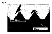
グリッド構造体(MASTER)をガラス転移温度Tg100℃のポリスチレン基材(N5000,Shell AG)にプレスすることによってポリマー基材上にチャネルのグリッドを製造した。この目的のために、MASTERを180℃に加熱し、小型プレス(Tribotrak,DACA Instruments,米国カリフォルニア州サンタバーバラ)を用いて基材に3kgの負荷で3分間プレスした。MASTERは、42μmのライン間隔を示し、MASTERにおけるくぼみは、断面で見ると、逆立ちしたカットオフトライアングル(cut−off triangles)のように見えた(図2)。MASTERにおける隆起は、高さ20μmを示し、更に、断面で見るとカットオフトライアングルである。MASTERにおける隆起の基底幅は32μmであり、隆起のピークの幅は約4.5μmであった。
Example 1
A grid of channels was fabricated on a polymer substrate by pressing the grid structure (MASTER) onto a polystyrene substrate (N5000, Shell AG) with a glass transition temperature Tg of 100 ° C. For this purpose, the MASTER was heated to 180 ° C. and pressed on a substrate with a 3 kg load for 3 minutes using a small press (Tribotrak, DACA Instruments, Santa Barbara, Calif., USA). The MASTER showed a line spacing of 42 μm, and the depression in the MASTER looked like a cut-off triangles when viewed in cross-section (FIG. 2). The ridge in the MASTER has a height of 20 μm and is a cut-off triangle when viewed in cross section. The base width of the ridge in the MASTER was 32 μm, and the width of the peak of the ridge was about 4.5 μm.
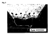
銀ナノインク(NanopasteTM,ハリマ化成株式会社,日本)の1つの液滴を上記のように製造したラインの1つに配置した。このインクは、テトラデカン中の平均径約5nmの銀ナノ粒子の分散体からなる。毛細管現象のために、インクのラインがチャネルに速やかに形成する。長さ約4mmの均一なラインを維持することが可能であった。インクジェットシステム(AutodropTMシステム;Microdrop Technologies,ドイツ国ノルダーシュテット)を用いてインク液滴の正確な位置合わせを達成した。このシステムは68μmのノズルヘッドを備えていた。もたらされる銀のラインの最大幅は、図3からわかるように、完全な高さで約6.3μmであった。最も狭い位置で幅約3.7μmであった(図3の基底参照。)。次に、基材を200℃において1.5時間調質し(temper)、インクを焼結銀からなる連続ラインに転化した。基底における窪みの幅(3.7μm)とMASTERプロファイルの対応する上縁の幅(4.5μm)との間のずれは、インク溶媒の影響下における基材の膨潤およびスタンピング中の基材の加熱によって説明できる。2.5Ωの抵抗が6mmの4本の平行ラインにおいて測定された。 One droplet of silver nanoink (Nanopathe ™, Harima Kasei Co., Ltd., Japan) was placed on one of the lines produced as described above. This ink consists of a dispersion of silver nanoparticles with an average diameter of about 5 nm in tetradecane. Due to capillary action, ink lines quickly form in the channel. It was possible to maintain a uniform line about 4 mm in length. Accurate alignment of the ink droplets was achieved using an inkjet system (Autodrop ™ system; Microdrop Technologies, Norderstedt, Germany). This system was equipped with a 68 μm nozzle head. The maximum width of the resulting silver line was about 6.3 μm at full height, as can be seen in FIG. The narrowest position was about 3.7 μm wide (see the base in FIG. 3). The substrate was then tempered at 200 ° C. for 1.5 hours, and the ink was converted to a continuous line of sintered silver. Deviations between the width of the depression at the base (3.7 μm) and the corresponding upper edge width of the MASTER profile (4.5 μm) are due to the swelling of the substrate under the influence of the ink solvent and heating of the substrate during stamping Can be explained by A resistance of 2.5Ω was measured on 4 parallel lines of 6 mm.
実施例2
ガラス転移温度Tg205℃のポリカーボネートフィルム(Bayfol(登録商標),Bayer MaterialScience AG)であって、270℃に加熱されたものにグリッドをプレスすることによってチャネルのグリッドを作り出した。他の全てのスタンピングパラメータは実施例1に相当した。実施例1と同じ方法で、伝導性ラインを作り出した。達せられたライン幅および導電性銀導体パスの長さは、実施例1において作り出されるパスのそれらと同じであった。
Example 2
A grid of channels was created by pressing the grid onto a polycarbonate film (Bayfol®, Bayer MaterialScience AG) with a glass transition temperature Tg of 205 ° C. heated to 270 ° C. All other stamping parameters corresponded to Example 1. Conductive lines were created in the same way as in Example 1. The achieved line width and conductive silver conductor path length were the same as those of the path created in Example 1.
実施例3
方法は実施例1と同じであったが、プレスダイを用いるスタンピング法の代わりにプレスローラーを使用した。
Example 3
The method was the same as in Example 1, but a press roller was used instead of the stamping method using a press die.
小型プレス(Tribotrak,DACA Instruments,米国カリフォルニア州サンタバーバラ)上に載置されたローラーを用いて厚さ10mmのポリカーボネート基材(Makrolon,Bayer,ドイツ国,ガラス転移温度148℃)上に連続構造体を作り出した。小型プレス上に載置された特別に仕上げられたローラーは、幅10μmかつ間隔3mmの浮出ライン状構造体を有していた。このアレンジメントにおいて、基材の表面を60℃に加熱し、ローラーの温度は155℃であった。プレスの圧力を、上述のアセンブリにおいて10kgの重しを用いてセットした。セットされる温度および使用される圧力に対してローラーから基材への相対駆動速度0.25mm/秒を選択した。このアレンジメントにおいて、上記相対速度を達成するために、基材をスライドによってローラーの下に沿って引っ張った。圧力はローラーが基材上で回転するのに十分であった。 Continuous structure on 10 mm thick polycarbonate substrate (Makrolon, Bayer, Germany, glass transition temperature 148 ° C.) using rollers mounted on a small press (Tribotrak, DACA Instruments, Santa Barbara, Calif.) Produced. A specially finished roller mounted on a small press had raised line-like structures with a width of 10 μm and a spacing of 3 mm. In this arrangement, the surface of the substrate was heated to 60 ° C., and the roller temperature was 155 ° C. The press pressure was set using a 10 kg weight in the above assembly. A relative drive speed from the roller to the substrate of 0.25 mm / sec was chosen for the temperature set and the pressure used. In this arrangement, to achieve the relative speed, the substrate was pulled along the bottom of the roller by a slide. The pressure was sufficient for the roller to rotate on the substrate.
Claims (6)
機械的および要すれば熱的効果によって、幅が10μm以下であるチャネルを基材表面に作り出す工程であって、ここで前記チャネルがプレスダイまたはプレスローラーを用いて基材の表面にスタンプされる、工程、
導電性構造体が作り出されることを可能にするインクを該チャネルに適用する工程、
毛細管現象によって該チャネルにインクを満たす工程、
エネルギーを導入することによってインクを導電性構造体に転化する工程
を包含し、
前記インクは、直径が100nm未満である銀ナノ粒子のサスペンジョンであることを特徴とする、方法。 A method for producing a conductive structure having a dimension of 10 μm or less in two dimensions on a particularly optically transparent substrate having a moldable surface, comprising:
Creating a channel on the surface of the substrate by mechanical and, if necessary, thermal effects, having a width of 10 μm or less , wherein the channel is stamped on the surface of the substrate using a press die or a press roller. Process,
Applying an ink to the channel that allows a conductive structure to be created;
Filling the channel with ink by capillary action;
Including the step of converting the ink into a conductive structure by introducing energy;
The method, wherein the ink is a suspension of silver nanoparticles having a diameter of less than 100 nm.
Applications Claiming Priority (5)
| Application Number | Priority Date | Filing Date | Title |
|---|---|---|---|
| DE102007033523.9 | 2007-07-19 | ||
| DE200710033523 DE102007033523A1 (en) | 2007-07-19 | 2007-07-19 | Conductive structures production involves generating channels on surface of substrate by mechanical effect, where ink is suspension of conductive particles and is applied on channels |
| DE102007043396.6 | 2007-09-12 | ||
| DE200710043396 DE102007043396A1 (en) | 2007-09-12 | 2007-09-12 | Method for manufacturing electrical conducting structures, involves producing channels on surface of substrate by mechanical and additionally thermal effects and ink is applied on channels |
| PCT/EP2008/005543 WO2009010208A1 (en) | 2007-07-19 | 2008-07-08 | Method for producing thin, conductive structures on surfaces |
Publications (3)
| Publication Number | Publication Date |
|---|---|
| JP2010533939A JP2010533939A (en) | 2010-10-28 |
| JP2010533939A5 JP2010533939A5 (en) | 2011-08-04 |
| JP5606908B2 true JP5606908B2 (en) | 2014-10-15 |
Family
ID=39929915
Family Applications (1)
| Application Number | Title | Priority Date | Filing Date |
|---|---|---|---|
| JP2010516400A Expired - Fee Related JP5606908B2 (en) | 2007-07-19 | 2008-07-08 | Method for producing a fine conductive structure on a surface |
Country Status (7)
| Country | Link |
|---|---|
| US (1) | US20090061213A1 (en) |
| EP (1) | EP2179633A1 (en) |
| JP (1) | JP5606908B2 (en) |
| KR (1) | KR20100044176A (en) |
| CN (1) | CN101755493A (en) |
| TW (1) | TW200924576A (en) |
| WO (1) | WO2009010208A1 (en) |
Families Citing this family (18)
| Publication number | Priority date | Publication date | Assignee | Title |
|---|---|---|---|---|
| TWI438906B (en) * | 2007-12-20 | 2014-05-21 | Cima Nanotech Israel Ltd | Photovoltaic device having transparent electrode formed with nanoparticles |
| KR101009442B1 (en) * | 2009-04-15 | 2011-01-19 | 한국과학기술연구원 | Method for fabrication of conductive film using conductive frame and conductive film |
| KR101145752B1 (en) * | 2010-07-20 | 2012-05-16 | 김용문 | Ink Composition For Printed Circuit Board |
| US9011651B2 (en) | 2010-12-09 | 2015-04-21 | Ut-Battelle, Llc | Apparatus and method for the electrolysis of water |
| KR101771138B1 (en) | 2011-05-13 | 2017-08-25 | 삼성전자주식회사 | Wire grid polarizer, method of fabricating the wire grid polarizer and display panel including the wire grid polarizer |
| KR101968635B1 (en) * | 2012-11-22 | 2019-04-12 | 삼성전자주식회사 | Method of forming electric wiring using inkjet printing and inkjet printing apparatus |
| CN106166792A (en) | 2015-10-16 | 2016-11-30 | 圣戈本陶瓷及塑料股份有限公司 | There is crystalline ceramics and its manufacture method of complex geometric shapes |
| JP6938024B2 (en) * | 2015-10-22 | 2021-09-22 | 国立研究開発法人産業技術総合研究所 | Surface structure of substrate to be printed and its manufacturing method |
| WO2019035094A1 (en) * | 2017-08-17 | 2019-02-21 | California Institute Of Technology | Fabrication processes for effectively transparent contacts |
| US11227964B2 (en) | 2017-08-25 | 2022-01-18 | California Institute Of Technology | Luminescent solar concentrators and related methods of manufacturing |
| JP2021515983A (en) * | 2018-03-06 | 2021-06-24 | スリーエム イノベイティブ プロパティズ カンパニー | Automatic alignment between circuit dies and interconnects |
| US11362229B2 (en) | 2018-04-04 | 2022-06-14 | California Institute Of Technology | Epitaxy-free nanowire cell process for the manufacture of photovoltaics |
| EP3572873A1 (en) * | 2018-05-24 | 2019-11-27 | Paul Scherrer Institut | Method for reducing the width of structures generated by ink deposition on pre-patterned substrates |
| WO2020041522A1 (en) | 2018-08-21 | 2020-02-27 | California Institute Of Technology | Windows implementing effectively transparent conductors and related methods of manufacturing |
| CN109395790B (en) * | 2018-12-11 | 2024-03-29 | 福州大学 | Paper-based composite three-dimensional micro/nano circuit and processing method thereof |
| US11939688B2 (en) | 2019-03-29 | 2024-03-26 | California Institute Of Technology | Apparatus and systems for incorporating effective transparent catalyst for photoelectrochemical application |
| US11745440B2 (en) * | 2020-04-03 | 2023-09-05 | The Boeing Company | Automated lamination system and method for embedding printed electronic elements in a composite structure |
| WO2023069739A1 (en) * | 2021-10-22 | 2023-04-27 | Worcester Polytechnic Institute | Microchannel printing |
Family Cites Families (16)
| Publication number | Priority date | Publication date | Assignee | Title |
|---|---|---|---|---|
| US5091339A (en) * | 1990-07-23 | 1992-02-25 | Microelectronics And Computer Technology Corporation | Trenching techniques for forming vias and channels in multilayer electrical interconnects |
| JP2900335B2 (en) * | 1992-08-06 | 1999-06-02 | アルプス電気株式会社 | Transfer printed wiring board |
| NL1008460C2 (en) * | 1998-03-03 | 1999-09-06 | Acheson Colloiden B V | Conductive ink or paint. |
| US6103033A (en) | 1998-03-04 | 2000-08-15 | Therasense, Inc. | Process for producing an electrochemical biosensor |
| SG108820A1 (en) * | 2001-02-23 | 2005-02-28 | Agency Science Tech & Res | Method and apparatus for forming a metallic feature on a substrate |
| US6896864B2 (en) * | 2001-07-10 | 2005-05-24 | Battelle Memorial Institute | Spatial localization of dispersed single walled carbon nanotubes into useful structures |
| US6887450B2 (en) * | 2002-01-02 | 2005-05-03 | Zyvex Corporation | Directional assembly of carbon nanotube strings |
| US6872645B2 (en) * | 2002-04-02 | 2005-03-29 | Nanosys, Inc. | Methods of positioning and/or orienting nanostructures |
| US6911385B1 (en) | 2002-08-22 | 2005-06-28 | Kovio, Inc. | Interface layer for the fabrication of electronic devices |
| US7013562B2 (en) * | 2003-03-31 | 2006-03-21 | Intel Corporation | Method of using micro-contact imprinted features for formation of electrical interconnects for substrates |
| US7618704B2 (en) * | 2003-09-29 | 2009-11-17 | E.I. Du Pont De Nemours And Company | Spin-printing of electronic and display components |
| US20060124028A1 (en) * | 2004-12-09 | 2006-06-15 | Xueying Huang | Inkjet ink compositions comprising carbon nanotubes |
| WO2006076603A2 (en) | 2005-01-14 | 2006-07-20 | Cabot Corporation | Printable electrical conductors |
| US8097400B2 (en) | 2005-02-22 | 2012-01-17 | Hewlett-Packard Development Company, L.P. | Method for forming an electronic device |
| WO2006100790A1 (en) | 2005-03-22 | 2006-09-28 | Cluster Technology Co., Ltd. | Process for producing wiring board, and wiring board |
| JP2007062254A (en) * | 2005-09-01 | 2007-03-15 | Dainippon Ink & Chem Inc | Method of molding laminated sheet for thermoforming |
-
2008
- 2008-07-08 EP EP08784642A patent/EP2179633A1/en not_active Withdrawn
- 2008-07-08 CN CN200880025345A patent/CN101755493A/en active Pending
- 2008-07-08 KR KR1020107001083A patent/KR20100044176A/en active IP Right Grant
- 2008-07-08 WO PCT/EP2008/005543 patent/WO2009010208A1/en active Application Filing
- 2008-07-08 JP JP2010516400A patent/JP5606908B2/en not_active Expired - Fee Related
- 2008-07-11 US US12/171,513 patent/US20090061213A1/en not_active Abandoned
- 2008-07-18 TW TW097127233A patent/TW200924576A/en unknown
Also Published As
| Publication number | Publication date |
|---|---|
| CN101755493A (en) | 2010-06-23 |
| TW200924576A (en) | 2009-06-01 |
| US20090061213A1 (en) | 2009-03-05 |
| JP2010533939A (en) | 2010-10-28 |
| WO2009010208A1 (en) | 2009-01-22 |
| KR20100044176A (en) | 2010-04-29 |
| EP2179633A1 (en) | 2010-04-28 |
Similar Documents
| Publication | Publication Date | Title |
|---|---|---|
| JP5606908B2 (en) | Method for producing a fine conductive structure on a surface | |
| Chang et al. | Direct writing and repairable paper flexible electronics using nickel–liquid metal ink | |
| Wisser et al. | Precursor strategies for metallic nano-and micropatterns using soft lithography | |
| CN104919572B (en) | Forming method, conducting film, conductive pattern and the nesa coating of conductive pattern | |
| KR20140113630A (en) | Aqueous ink formulation containing metal-based nanoparticles for usage in microcontact printing | |
| US20090074955A1 (en) | Methods for patterning electronic elements and fabricating molds | |
| CN104583814A (en) | Antifouling body, display device, input device, and electronic device | |
| Lee et al. | High-resolution conductive patterns fabricated by inkjet printing and spin coating on wettability-controlled surfaces | |
| Chen et al. | Self-assembly, alignment, and patterning of metal nanowires | |
| CN107850958B (en) | Patterned overcoat | |
| Zhou et al. | Fabrication of conductive paths on a fused deposition modeling substrate using inkjet deposition | |
| Jambhulkar et al. | A multimaterial 3D printing-assisted micropatterning for heat dissipation applications | |
| Suganuma et al. | Printing Technology | |
| JP2007110054A (en) | Pattern forming method and pattern-formed substrate | |
| Sung et al. | Fabrication of high-resolution conductive lines by combining inkjet printing with soft lithography | |
| JP2013142158A (en) | Metallic nanostructure and method for producing the same | |
| WO2019224007A1 (en) | Method for reducing the width of structures generated by ink deposition on pre-patterned substrates | |
| US11284521B2 (en) | Electronic devices comprising a via and methods of forming such electronic devices | |
| Choi et al. | Direct imprint of conductive silver patterns using nanosilver particles and UV curable resin | |
| Keum et al. | Principle of topography-directed inkjet printing for functional micro-tracks in flexible substrates | |
| KR20170040070A (en) | A method of manufacturing metal stamps | |
| KR101717952B1 (en) | Elastic mold for direct imprinting and method for manufacturing electrode using the same | |
| US20210162788A1 (en) | Method for manufacturing an optical element | |
| DE102007043396A1 (en) | Method for manufacturing electrical conducting structures, involves producing channels on surface of substrate by mechanical and additionally thermal effects and ink is applied on channels | |
| Choi et al. | Direct imprinted conductive patterns using nanosilver colloid-applied UV curable resist |
Legal Events
| Date | Code | Title | Description |
|---|---|---|---|
| A521 | Written amendment |
Free format text: JAPANESE INTERMEDIATE CODE: A523 Effective date: 20110615 |
|
| A621 | Written request for application examination |
Free format text: JAPANESE INTERMEDIATE CODE: A621 Effective date: 20110615 |
|
| A711 | Notification of change in applicant |
Free format text: JAPANESE INTERMEDIATE CODE: A711 Effective date: 20130417 |
|
| A131 | Notification of reasons for refusal |
Free format text: JAPANESE INTERMEDIATE CODE: A131 Effective date: 20130604 |
|
| A711 | Notification of change in applicant |
Free format text: JAPANESE INTERMEDIATE CODE: A711 Effective date: 20130812 |
|
| A601 | Written request for extension of time |
Free format text: JAPANESE INTERMEDIATE CODE: A601 Effective date: 20130903 |
|
| A602 | Written permission of extension of time |
Free format text: JAPANESE INTERMEDIATE CODE: A602 Effective date: 20130910 |
|
| A601 | Written request for extension of time |
Free format text: JAPANESE INTERMEDIATE CODE: A601 Effective date: 20131003 |
|
| A602 | Written permission of extension of time |
Free format text: JAPANESE INTERMEDIATE CODE: A602 Effective date: 20131010 |
|
| A521 | Written amendment |
Free format text: JAPANESE INTERMEDIATE CODE: A523 Effective date: 20131031 |
|
| A131 | Notification of reasons for refusal |
Free format text: JAPANESE INTERMEDIATE CODE: A131 Effective date: 20131126 |
|
| RD04 | Notification of resignation of power of attorney |
Free format text: JAPANESE INTERMEDIATE CODE: A7424 Effective date: 20131219 |
|
| A601 | Written request for extension of time |
Free format text: JAPANESE INTERMEDIATE CODE: A601 Effective date: 20140225 |
|
| A602 | Written permission of extension of time |
Free format text: JAPANESE INTERMEDIATE CODE: A602 Effective date: 20140304 |
|
| A521 | Written amendment |
Free format text: JAPANESE INTERMEDIATE CODE: A523 Effective date: 20140313 |
|
| A131 | Notification of reasons for refusal |
Free format text: JAPANESE INTERMEDIATE CODE: A131 Effective date: 20140408 |
|
| A521 | Written amendment |
Free format text: JAPANESE INTERMEDIATE CODE: A523 Effective date: 20140704 |
|
| TRDD | Decision of grant or rejection written | ||
| A01 | Written decision to grant a patent or to grant a registration (utility model) |
Free format text: JAPANESE INTERMEDIATE CODE: A01 Effective date: 20140729 |
|
| A61 | First payment of annual fees (during grant procedure) |
Free format text: JAPANESE INTERMEDIATE CODE: A61 Effective date: 20140827 |
|
| R150 | Certificate of patent or registration of utility model |
Ref document number: 5606908 Country of ref document: JP Free format text: JAPANESE INTERMEDIATE CODE: R150 |
|
| LAPS | Cancellation because of no payment of annual fees |