JP5606090B2 - Method for digitally programmable optimization of hybrid signal circuits - Google Patents
Method for digitally programmable optimization of hybrid signal circuits Download PDFInfo
- Publication number
- JP5606090B2 JP5606090B2 JP2010027440A JP2010027440A JP5606090B2 JP 5606090 B2 JP5606090 B2 JP 5606090B2 JP 2010027440 A JP2010027440 A JP 2010027440A JP 2010027440 A JP2010027440 A JP 2010027440A JP 5606090 B2 JP5606090 B2 JP 5606090B2
- Authority
- JP
- Japan
- Prior art keywords
- bias
- transistor
- body tie
- voltage
- signal circuit
- Prior art date
- Legal status (The legal status is an assumption and is not a legal conclusion. Google has not performed a legal analysis and makes no representation as to the accuracy of the status listed.)
- Expired - Fee Related
Links
Images


Classifications
-
- H—ELECTRICITY
- H03—ELECTRONIC CIRCUITRY
- H03F—AMPLIFIERS
- H03F1/00—Details of amplifiers with only discharge tubes, only semiconductor devices or only unspecified devices as amplifying elements
- H03F1/30—Modifications of amplifiers to reduce influence of variations of temperature or supply voltage or other physical parameters
- H03F1/301—Modifications of amplifiers to reduce influence of variations of temperature or supply voltage or other physical parameters in MOSFET amplifiers
-
- G—PHYSICS
- G05—CONTROLLING; REGULATING
- G05F—SYSTEMS FOR REGULATING ELECTRIC OR MAGNETIC VARIABLES
- G05F1/00—Automatic systems in which deviations of an electric quantity from one or more predetermined values are detected at the output of the system and fed back to a device within the system to restore the detected quantity to its predetermined value or values, i.e. retroactive systems
- G05F1/10—Regulating voltage or current
- G05F1/46—Regulating voltage or current wherein the variable actually regulated by the final control device is dc
-
- H—ELECTRICITY
- H03—ELECTRONIC CIRCUITRY
- H03F—AMPLIFIERS
- H03F1/00—Details of amplifiers with only discharge tubes, only semiconductor devices or only unspecified devices as amplifying elements
- H03F1/30—Modifications of amplifiers to reduce influence of variations of temperature or supply voltage or other physical parameters
- H03F1/303—Modifications of amplifiers to reduce influence of variations of temperature or supply voltage or other physical parameters using a switching device
- H03F1/304—Modifications of amplifiers to reduce influence of variations of temperature or supply voltage or other physical parameters using a switching device and using digital means
-
- H—ELECTRICITY
- H03—ELECTRONIC CIRCUITRY
- H03F—AMPLIFIERS
- H03F2200/00—Indexing scheme relating to amplifiers
- H03F2200/366—Multiple MOSFETs are coupled in parallel
Description
本発明は、混成信号回路のデジタル式プログラム可能な最適化のための方法に関する。 The present invention relates to a method for digital programmable optimization of hybrid signal circuits.
混成信号回路は、トランジスタの不整合に敏感である。よく知られているPelgromモデルでは、同じダイ上の2つの素子の間のランダム不整合に起因するばらつきは、素子面積の平方根に反比例することが実証されている。トランジスタの不整合効果は、トランジスタの小型化に伴い更に悪化するので、高速混成信号回路設計では、不整合効果が歩留まり及び性能の有力な制限要因になっている。このような不整合効果のせいで、アナログ及び無線周波数(RF)回路は、それぞれの新しいプロセス技術ノードで利用可能なトランジスタ尺度化から恩恵を受けることが益々難しくなっている。不整合効果に対処するために幾つかの手法が開発されてきたが、それらは全て様々な制限に悩まされている。 Hybrid signal circuits are sensitive to transistor mismatch. The well-known Pelgrom model demonstrates that variations due to random mismatch between two devices on the same die are inversely proportional to the square root of the device area. Since the transistor mismatch effect is further aggravated with the miniaturization of the transistor, the mismatch effect has become a significant limiting factor in yield and performance in high speed hybrid signal circuit design. Because of such mismatch effects, analog and radio frequency (RF) circuits are becoming increasingly difficult to benefit from transistor scaling available at each new process technology node. Several approaches have been developed to deal with inconsistent effects, but they all suffer from various limitations.
例えば、デジタル回路動作には、ダイ間及びダイ内のばらつきについてポストプロセス調整を提供するために、アダプティブ・ボディ・バイアス(ABB)技法が適用されている。とはいえ、開発努力の殆どは、必要なボディバイアス調整を施すために精密なアナログ電圧を作り出す1つ又はそれ以上の複合的なアナログ式ボディバイアス発生器の実装と調整に向けられてきた。類似の技法を混成信号回路に適用することもできるかもしれないが、アナログ式ボディバイアス発生器の追加は、それらをそれぞれの臨界サブ回路ノードのボディ端子まで通さねばならないため、複数の面積が食いつぶされることを犠牲にしなければならないと推測される。 For example, adaptive body bias (ABB) techniques have been applied to digital circuit operation to provide post-process adjustment for die-to-die and within-die variations. Nonetheless, most of the development effort has been directed to the implementation and adjustment of one or more complex analog body bias generators that produce precise analog voltages to provide the necessary body bias adjustments. Similar techniques may be applied to hybrid signal circuits, but the addition of analog body bias generators takes multiple areas because they must be routed to the body terminals of each critical subcircuit node. It is speculated that it must be sacrificed to be crushed.
或いは、アナログ回路については、並列に接続された複数の差動対の物理的実装と所望の整合レベルを実現するサブセットの選択を伴う技法が提案されている。この手法では、余分なシリコン面積とゲートキャパシタンスの増大が重大な制限事項になっている。 Alternatively, for analog circuits, techniques have been proposed that involve the physical implementation of multiple differential pairs connected in parallel and the selection of a subset that achieves the desired matching level. In this approach, extra silicon area and increased gate capacitance are significant limitations.
本発明は、混成信号回路のデジタル式プログラム可能な最適化のための方法に関する。この方法は、混成信号回路の1つ又はそれ以上のトランジスタ素子を、1つ又はそれ以上のトランジスタ区分に、それぞれのトランジスタ区分がボディタイバイアス端子を含むようにして、分割することを含んでいる。ぞれぞれのボディタイバイアス端子は、少なくとも1つの電圧バイアスに、それぞれのボディタイバイアス端子を混成信号回路の1つ又はそれ以上のバイアスノードと信号連通させるか、又はそれぞれのボディタイバイアス端子を非精密バイアス電圧ソースと信号連通させるかの何れかによって、連結される。各々のボディタイ端子は、更に、1つ又はそれ以上のデジタル式プログラム可能な記憶要素の別々の1つと信号連通するように配置される。 The present invention relates to a method for digital programmable optimization of hybrid signal circuits. The method includes dividing one or more transistor elements of the hybrid signal circuit into one or more transistor sections, each transistor section including a body tie bias terminal. Each body tie bias terminal communicates at least one voltage bias with each body tie bias terminal in signal communication with one or more bias nodes of the hybrid signal circuit or with each body tie bias terminal. Are either in signal communication with a non-precision bias voltage source. Each body tie terminal is further arranged in signal communication with a separate one of one or more digitally programmable storage elements.
当業者には、図面を参照しながら以下の説明を読んで頂ければ、本発明の特徴が明らかになるであろう。図面は本発明の代表的な実施形態を描いているに過ぎず、従って、本発明の範囲に限定を課すものと考えられるべきではないことが理解された上で、添付図面を用いながら本発明を更に明確に詳しく説明してゆく。 The features of the present invention will become apparent to those skilled in the art when the following description is read with reference to the drawings. It is understood that the drawings depict only typical embodiments of the invention and, therefore, should not be considered as limiting the scope of the invention, and the invention is described with reference to the accompanying drawings. Will be explained more clearly and in detail.
以下の詳細な説明では、各実施形態は、当業者が本発明を実践することができるように十分に詳細に説明されている。なお、本発明の範囲を逸脱することなく、他の実施形態を利用することもできるものと理解頂きたい。従って、以下の詳細な説明は、制限を課すという意味で捉えられるべきではない。 In the following detailed description, each embodiment is described in sufficient detail to enable those skilled in the art to practice the invention. It should be understood that other embodiments may be utilized without departing from the scope of the present invention. Accordingly, the following detailed description should not be taken in the sense of imposing limitations.
本発明は、歩留まりを改善し、性能を向上させ、パワー消費量を削減する、混成信号回路のデジタル式プログラム可能な最適化のためのシステム及び方法に関する。本発明の技法は、概括的には、個々のトランジスタをより小さい区分に分割することと、それぞれの区分のボディを、既に利用可能になっているバイアスノード又は単純な非精密バイアス電圧に個別に接続することを含んでいる。これにより、複合的なトランジスタ特性を、要求される精密度に調整することができるようになり、臨界ノード毎の複数の精密バイアス発生器の必要がなくなる。それら臨界回路ノードにおけるトランジスタ特性をプロセス後に調整できるようにすることによって、最適回路動作に必要な整合が実現される。 The present invention relates to systems and methods for digitally programmable optimization of hybrid signal circuits that improve yield, improve performance, and reduce power consumption. The technique of the present invention generally divides individual transistors into smaller sections and separates the body of each section individually into bias nodes or simple non-precision bias voltages that are already available. Includes connecting. This allows complex transistor characteristics to be adjusted to the required precision, eliminating the need for multiple precision bias generators per critical node. By allowing the transistor characteristics at these critical circuit nodes to be adjusted post-process, the matching required for optimal circuit operation is achieved.
本手法は、トランジスタとプロセスが引き起こすトランジスタ不整合に付随する、混成信号の歩留まり及び性能に限界を生じさせる業界規模の尺度化に課せられた制限の問題解決に対処している。それらの問題は、相補型金属酸化膜半導体(CMOS)の新しい技術ノードが導入されるたびに悪化する。本技法は、トランジスタ密度を改善し、不整合に起因する尺度化制限に対する実行可能な解決策を提供している。例えば、本発明の方法では、150nm、90nm、及びより先進的な技術で、プロセスとトランジスタの不整合特性をプロセス後に補正することができるようになる。 This approach addresses the problem of limitations imposed by industry-scale scaling that limits the yield and performance of mixed signals associated with transistor mismatch caused by transistors and processes. These problems are exacerbated with the introduction of new technology nodes for complementary metal oxide semiconductors (CMOS). This technique improves transistor density and provides a viable solution to scaling limitations due to mismatch. For example, the method of the present invention allows the process and transistor mismatch characteristics to be corrected post-process with 150 nm, 90 nm, and more advanced technologies.
本手法は、混成信号回路構成のみならず、デジタル回路構成においても使用することができる。そのような回路構成は、既知の技法によって耐放射線性を持たせることもできる。本手法は、歩留まりの最大化、及びアナログ用とデジタル用の両方の自己修復回路の作製に非常に有用である。本技法では、臨界ノードトランジスタのゲート面積を削減することができ、回路動作に必要な速度とパワーの両方を向上させることができる。 This technique can be used not only in a hybrid signal circuit configuration but also in a digital circuit configuration. Such circuit configurations can also be made radiation resistant by known techniques. This approach is very useful for maximizing yield and creating both analog and digital self-healing circuits. With this technique, the gate area of the critical node transistor can be reduced, and both the speed and power required for circuit operation can be improved.
本回路設計技法では、混成信号回路で普通に利用できるバイアス電圧を使用して、トランジスタボディ端子を単純なトランジスタスイッチを介して接続させることができる代わりの電圧を提供している。これにより、個々のトランジスタは、プロセスによるダイ間のばらつきと個々の素子の不整合の両方について調整を施すために、異なるバイアスに接続することができるようになる。最適な回路機能のための所望の整合解決策を実現するために、トランジスタは、平均トランジスタ特性が設計ウィンドウ内に収まるように調整するのに必要なバイアスノードに切り替えることができる各自個別のボディバイアス端子をぞれぞれが備えているn個の区分に分割される。 The circuit design technique provides an alternative voltage that allows the transistor body terminals to be connected through a simple transistor switch using a bias voltage commonly available in hybrid signal circuits. This allows individual transistors to be connected to different biases in order to adjust for both process-to-die variation and individual device mismatch. In order to achieve the desired matching solution for optimal circuit function, each transistor can be switched to a bias node necessary to adjust the average transistor characteristics to be within the design window. The terminal is divided into n sections each provided.
デジタル回路制御論理と混成信号回路構成の間の物理的インターフェースは、ボディタイ端子を通して達成することができる。標準的なシリコン・オン・インシュレータ(SOI)回路設計技法は、ボディタイ端子のこと、それをソース又は電源の何れかに接続することを無視している。更に、商業的に最も利用可能なSOI CMOSプロセスでは、ボディの接続には、ゲートキャパシタンスの増大という多大なオーバーヘッドの不利益を被ることが伴う。これらの問題は、個々のボディタイ接続をゲートキャパシタンスを著しく増大させることなく効率的に実装するよう設計された、本手法のSOI CMOSプロセスへの実装によって解決が図られている。個々のボディタイ接続を作製する場合のこのSOIプロセスの効率の良さにより、バルクCMOSを同じように構成しようとした場合に必要になるトリプルウェルのような追加のプロセス工程を導入することなしに、面積への影響を最小限に抑えることができる。 The physical interface between the digital circuit control logic and the hybrid signal circuitry can be achieved through body tie terminals. Standard silicon-on-insulator (SOI) circuit design techniques ignore the body tie terminal, connecting it to either the source or the power supply. Furthermore, in the most commercially available SOI CMOS process, the connection of the body is associated with a significant overhead penalty of increased gate capacitance. These problems are addressed by the implementation of this approach in SOI CMOS processes, designed to efficiently implement individual body tie connections without significantly increasing gate capacitance. The efficiency of this SOI process when making individual body tie connections allows for the introduction of additional process steps such as triple wells that would be required if the bulk CMOS was to be configured in the same way. The influence on the area can be minimized.
回路のスイッチは、デジタル式フリップフロップのようなデジタル式プログラム可能な記憶要素を用いて制御することができ、同要素は、幾つかの実施形態では、デジタル式リアルタイム性能最適化制御システムへのインターフェースを提供することができる。本技法は、単純な非精密バイアス発生器を関心対象のサブ回路に局所的に追加すれば、デジタル回路に適用することができる。非精密バイアス発生器は、必要に応じ、アナログ回路に追加することもできる。 Circuit switches can be controlled using digitally programmable storage elements such as digital flip-flops, which in some embodiments interface to a digital real-time performance optimization control system. Can be provided. The technique can be applied to digital circuits if a simple non-precision bias generator is added locally to the subcircuit of interest. Non-precision bias generators can be added to the analog circuitry as needed.
本方法を使用して、最大SerDes(シリアライザ/デシリアライザ)周波数を、3.125GHzから、次に高い作動周波数ノードの4.25GHz、そして恐らくは6GHzまで上げることができる。 Using this method, the maximum SerDes (serializer / deserializer) frequency can be increased from 3.125 GHz to the next higher operating frequency node, 4.25 GHz, and possibly 6 GHz.
本発明のシステム及び方法の更なる詳細を、図面を参照しながら以下に説明する。
トランジスタボディタイ
本手法は、トリプルウェルバルクプロセス及び非ボディタイ型SOI技術で実装することもできるが、面積効率の高いボディタイ型SOI技術で実装するのが最も有利である。本技法を実装するのに使用されるSOI技術の固有特性は、「ボディタイ」と呼ばれる、接続部のトランジスタのボディへの面積効率の高い集積化である。ボディタイは、ヒステリシスと、混成信号設計を非常に難しくする他のフローティングボディ効果を排除する。ボディタイ接続は、ゲートキャパシタンスを増大させないので、周波数応答を、高速混成信号回路設計に対応できるように最大化することができる。
Further details of the system and method of the present invention are described below with reference to the drawings.
Transistor body tie Although this technique can be implemented with a triple well bulk process and non-body tie SOI technology, it is most advantageous to implement with a body tie SOI technology with high area efficiency. An inherent property of SOI technology used to implement this technique is an area efficient integration into the body of the transistor of the connection, referred to as a “body tie”. Body ties eliminate hysteresis and other floating body effects that make hybrid signal design very difficult. Since the body tie connection does not increase the gate capacitance, the frequency response can be maximized to accommodate high speed hybrid signal circuit designs.
ボディタイ端子が利用可能になったことで、各個別のトランジスタの性能特性に対する追加的な入力が提供されることになり、これを利用すれば、普通のプロセスばらつきとトランジスタの不整合を補償することによって性能設計の限界が広がるように臨界性能ノードを調整することができるようになる。更に、ボディタイ端子がSOIプロセスで利用可能になったことで、混成信号回路をシステム修復アーキテクチャに組み込めば、歩留まりと性能の両方を修復する実用的なやり方を提供することができる。
混成信号回路実施形態
図1は、本発明の1つの実施形態によるn状態デジタル制御式混成信号トランジスタ素子100の回路図である。トランジスタ素子100は、様々な幅の複数のトランジスタ区分T1、T2、…Tnに分割されており、各トランジスタ区分は、個別に制御されるボディバイアスを有している。トランジスタ区分の数は、アプリケーションの詳細に従い、面積と必要な制御の精密度の間の費用/利益分析を使って求められる。
The availability of body tie terminals provides an additional input for the performance characteristics of each individual transistor, which can be used to compensate for normal process variations and transistor mismatches. As a result, the critical performance node can be adjusted so that the limit of the performance design is expanded. In addition, the availability of body tie terminals in the SOI process can provide a practical way to repair both yield and performance if hybrid signal circuits are incorporated into the system repair architecture.
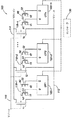
Hybrid Signal Circuit Embodiment FIG. 1 is a circuit diagram of an n-state digitally controlled hybrid
それぞれのトランジスタ区分のソース領域は、電圧ソース(Vソース)バス112に連結され、ドレイン領域は、電圧ドレイン(Vドレイン)バス114に連結されている。トランジスタ区分のゲートは、電圧ゲート(Vゲート)バス116に連結されている。実際の閾値電圧は、各トランジスタ区分の閾値の加重平均である。
The source region of each transistor section is coupled to a voltage source (V source)
トランジスタ区分T1からTnのそれぞれは、一対の最小サイズのインターフェーストランジスタN1及びN2を通して電圧V1又はV2に接続されている独立したボディタイバイアス端子118−1から118−nを有している。インターフェーストランジスタN1、N2はといえば、トランジスタN1、N2のゲートG1、G2で、各自のn制御フリップフロップ(CFF)122−1から122−nに連結されている。これにより、トランジスタ素子100の正味特性がCFFの状態によって決まるようにすることができる。電圧V1及びV2は、Vソースを含んでいる混成信号回路で利用可能な何れのバイアスであってもよい。区分T1からTnまでのトランジスタ幅は、トランジスタ素子の有効閾値と電流を規定のウィンドウ内に収まるように修正するのに必要な一定度の調整が許容されるように選択される。得られたトランジスタ平均閾値電圧は、V1、V2及びnフリップフロップの状態に応じて2n値に制御されることになる。
Each of the transistor sections T1 to Tn has an independent body tie bias terminal 118-1 to 118-n connected to a voltage V1 or V2 through a pair of minimum size interface transistors N1 and N2. Speaking of the interface transistors N1 and N2, the gates G1 and G2 of the transistors N1 and N2 are connected to the respective n control flip-flops (CFF) 122-1 to 122-n. Thereby, the net characteristic of the
アプリケーションの詳細に応じ、回路設計者は、本手法を、プロセス及び温度ばらつき並びに不整合について調整するのに使用してもよい。多くの用途では、単一のフリップフロップで十分であり、設計者にはトランジスタ幅の全部を制御するか又は一部だけを制御するかの選択肢がある。 Depending on the details of the application, circuit designers may use this approach to adjust for process and temperature variations and mismatches. For many applications, a single flip-flop is sufficient and the designer has the option of controlling all or only part of the transistor width.
図2は、本発明のもう1つの実施形態によるn状態デジタル制御式混成信号トランジスタ素子200の回路図である。トランジスタ素子200は、トランジスタ区分T1からTnに分割されており、それぞれのトランジスタ区分は個別に制御されるボディバイアスを有している。それぞれのトランジスタ区分のソース領域は、Vソースバス212に連結され、ドレイン領域はVドレインバス214に連結されている。トランジスタ区分のゲートはVゲートバス216に連結されている。
FIG. 2 is a circuit diagram of an n-state digitally controlled hybrid
トランジスタ区分のそれぞれは、最小サイズのインターフェーストランジスタN1を通して電圧V1に、そして最小サイズのインターフェーストランジスタP2を通して電圧V2に接続されている、独立したボディタイバイアス端子218−1から218−nを有している。各トランジスタ区分のインターフェーストランジスタN1とP2のそれぞれは、単一の制御ライン230−1から230−nを使用して、各自のn制御フリップフロップ222−1から222−nに連結されている。 Each of the transistor sections has independent body tie bias terminals 218-1 through 218-n connected to voltage V1 through minimum size interface transistor N1 and to voltage V2 through minimum size interface transistor P2. Yes. Each interface transistor N1 and P2 in each transistor segment is coupled to its own n-control flip-flops 222-1 to 222-n using a single control line 230-1 to 230-n.
このトランジスタ素子200の構成は、電圧V2がVソースより大きいときに有用である。これは、1つの制御ラインを制御フリップフロップから両インターフェーストランジスタN1とP2へ配線できるようにする。1つの実施形態では、V2がVソースより約0.6V大きいとき、トランジスタP2とボディタイバイアス端子218の間に電流制限抵抗器232を差し挟むこともできる。電圧V2は、正の供給電圧(Vdd)に接続されている1つ又はそれ以上のダイオード(図示せず)を用いて局所的に発生させることができる。例えば、Vdd=1.8Vのとき、直列につながれた3つのダイオードなら、約1.8/4=0.45Vのボディバイアスを発生させることになる。同じダイオードを使用して、同時に複数の区分でV2を発生させることもできる。
This configuration of the
図1と図2のインターフェーストランジスタN1、N2、及びP2は、それらのボディがソース端子に接続されているものとして示されている。多くの用途では、この構成は必須ではなく、フローティングにしておけば、物理的実装に必要なレイアウト面積を縮小することができる。 The interface transistors N1, N2, and P2 of FIGS. 1 and 2 are shown as having their bodies connected to the source terminal. In many applications, this configuration is not essential, and if left floating, the layout area required for physical mounting can be reduced.
図3は、本発明の別の実施形態によるn状態デジタル制御式混成信号トランジスタ素子300の回路図である。トランジスタ素子300は、トランジスタ区分T1からTnに分割されており、それぞれのトランジスタ区分は、個別に制御されるボディバイアスを有している。それぞれのトランジスタ区分のソース領域は、Vソースバス312に連結され、ドレイン領域は、Vドレインバス314に連結されている。トランジスタ区分のゲートはVゲートバス316に連結されている。トランジスタ区分のそれぞれは、何らのインターフェーストランジスタも差し挟まずに、単一の制御ライン330−1から330−nと抵抗器332−1から332−nを使用して各自のn制御フリップフロップ322−1から322−nに接続されている、独立したボディタイバイアス端子318−1から318−nを有している。
FIG. 3 is a circuit diagram of an n-state digitally controlled hybrid
このトランジスタ素子300の構成は、電圧V1とV2が、それぞれ、Vss(負の供給電圧)とVddであるときに有用である。その場合、それぞれのトランジスタ区分のボディタイは、抵抗器を通してフリップフロップに直接接続することができるので、面積への影響が最小限になる。
This configuration of the
図2と図3のトランジスタ素子を回路で使用する場合の特定の使用法に応じて、トランジスタ区分の制御フリップフロップの厳密な効果を巧みに操作するのに、トランジスタ、ダイオード、及び抵抗要素の様々な組合せを採用することもできる。
PLL実装
図4は、本発明の技法により修正された位相固定ループ(PLL)で使用される電圧制御式発振器(VCO)回路の形態をしている混成信号回路400の回路図である。このような混成信号回路では、バイアス電圧V1、V2についての代わりの選択肢が既に利用可能になっており、追加のパワー発生回路構成は不要である。回路400は、トランジスタの差動対TRとTLを含んでいる。それぞれのトランジスタ用のボディタイ端子410−1、410−2は、ソース又はグランドの何れかに接続することができる。
Depending on the particular use of the transistor elements of FIGS. 2 and 3 in a circuit, a variety of transistors, diodes, and resistor elements can be used to manipulate the exact effects of the transistor section control flip-flops. Various combinations can also be adopted.
PLL Implementation FIG. 4 is a circuit diagram of a
代表的な1.8V回路設計では、トランジスタの差動対のソース電圧とグランドの差は約0.3Vであり、閾値電圧(Vt)が約40−50mV調整されることになる。約40−50mVのVt不整合を取り除くことができる性能により、最小ゲート長さのトランジスタを使用することができるようになり、必要なゲート面積が大幅に削減される。 In a typical 1.8V circuit design, the difference between the source voltage and ground of the differential pair of transistors is about 0.3V, and the threshold voltage (Vt) will be adjusted by about 40-50 mV. The ability to remove a Vt mismatch of about 40-50 mV allows the use of a minimum gate length transistor, greatly reducing the required gate area.
Vtに約40mV増分の調整を施すことができる性能により、それぞれのトランジスタ用の単一のフリップフロップに、+/−20mVの整合を実現させることができる。20mVを凌ぐ整合が必要とされる回路設計では、図4のトランジスタTRとTLは、図1に関連して上で説明したようにn個の区分に分割することができる。トランジスタを幅の等しい2つの区分に分割すると、整合能力は2倍分向上する。更に、2つの区分の内の1つを2分割すると、整合能力は更に2倍分向上する。分割毎に、トランジスタの新しい区分を制御するための追加のフリップフロップが必要になる。 With the ability to adjust Vt in increments of about 40 mV, a single flip-flop for each transistor can achieve +/− 20 mV matching. In the circuit design matching surpassing 20mV is required, transistors T R and T L in FIG. 4 can be divided into n segments as described above in connection with FIG. If the transistor is divided into two equal width sections, the matching capability is improved by a factor of two. Furthermore, if one of the two sections is divided into two, the matching capability is further improved by a factor of two. Each division requires an additional flip-flop to control a new section of the transistor.
図4に示すように、例えば、トランジスタTRとTL用のボディタイ端子410−1と410−2のそれぞれは、一対のインターフェーストランジスタN1、N2を通してVsに接続されている。それぞれのインターフェーストランジスタN1、N2は、トランジスタの差動対TRとTLのボディをどの電圧ノードに接続するかを確定するデジタルラッチ又はフリップフロップの出力QL及びQRに連結されている。 As shown in FIG. 4, for example, each of body tie terminals 410-1 of the transistor T R and T L and 410-2 are connected to Vs through a pair of interface transistors N1, N2. Each interface transistors N1, N2 is connected to the output Q L and Q R of the digital latch or flip-flop to determine whether to connect the body of the differential pair T R and T L of the transistor to which voltage node.
このように、必要な整合の仕様と必要な制御ビットの数の間に存在する関係は単純である。しかしながら、この臨界トランジスタのn個の区分への分割は、これに伴う追加の寄生キャパシタンスが小さいために、速度及びパワーに関する多大な不利益を伴わない。実際、所与の必要な整合精密度については、本手法は常に最良の速度/パワー比を生み出すことができ、というのも標準的な方法を使用した場合は、整合はトランジスタのゲート面積の自乗に比例して向上するが、同様に速度は下がりパワーは上がるという結果しかもたらさないからである。 Thus, the relationship that exists between the required matching specifications and the number of required control bits is simple. However, the division of this critical transistor into n sections does not involve significant speed and power penalties due to the small additional parasitic capacitance associated therewith. In fact, for a given required matching accuracy, this approach can always produce the best speed / power ratio, since when using the standard method, matching is the square of the transistor gate area. This is because the speed decreases and the power increases as well.
本手法を使用したPLL実装を分析したところ、最小サイズのインターフェーススイッチトランジスタの追加が伴っても、混成信号回路トランジスタ面積の15−30%削減を実現することができ、同時に高速回路のゲート面積の40−80%削減、ACパワーの減少又は最大速度の増加を実現できることが示唆された。局部記憶フリップフロップと制御回路構成の引き換え加算分に費やされる面積は、所望される速度と高度化と制御インターフェースノードの数の関数であるが、合理的な推定値は、正味増分ゼロと総トランジスタ面積倍化が総PLL面積の約10%未満に納まる間のどこかになるであろう。
システム実装と動作
或る例示的なシステム実装では、前述の混成信号回路ノードのデジタル制御式トランジスタは、動作時、環境又は速度/パワー要件の変化を勘案するように、回路に集積されているシステムレベル又は局所の制御エンジンで動的にプログラムすることができる。例えば、1つの実施形態では、フリップフロップにデジタルコントローラを接続することができる。そのような構成が図1に示されており、同構成では、コントローラ130は、制御フリップフロップ1221から122−nとインターフェースさせることができる。コントローラは、混成信号回路とオンチップ集積化することもできるし、オフチップにすることもできる。フリップフロップは、コントローラによって読み込まれるように連続走査モードで接続することもできる。
Analysis of PLL implementation using this technique shows that even with the addition of the minimum size interface switch transistor, a 15-30% reduction in the area of the hybrid signal circuit transistor can be achieved, and at the same time the gate area of the high-speed circuit can be reduced. It was suggested that a 40-80% reduction, a decrease in AC power or an increase in maximum speed could be realized. The area spent on the exchange addition of local storage flip-flops and control circuitry is a function of the desired speed, sophistication, and number of control interface nodes, but a reasonable estimate is a net increment of zero and total transistors It will be somewhere while the area doubling falls below about 10% of the total PLL area.
System Implementation and Operation In one exemplary system implementation, the digitally controlled transistor of the hybrid signal circuit node described above is integrated into a circuit to account for changes in environment or speed / power requirements during operation. It can be dynamically programmed with a level or local control engine. For example, in one embodiment, a digital controller can be connected to the flip-flop. Such a configuration is shown in FIG. 1, in which the
コントローラは、当業者に知られているように、ソフトウェア、ファームウェア、ハードウェア、又はそれらの何らかの適切な組合せを使用して実装することができる。一例として、ハードウェア構成要素には、1つ又はそれ以上のマイクロプロセッサ、メモリ要素、デジタル信号処理(DSP)要素、インターフェースカード、及び当技術で既知の他の標準的な構成要素を挙げることができる。前記は何れも、1つ又はそれ以上の特別に設計された特定用途向け集積回路(ASIC)又はフィールド・プログラマブル・ゲート・アレイ(FPGA)によって補完されていてもよいし、又はそれに組み込まれていてもよい。 The controller may be implemented using software, firmware, hardware, or any suitable combination thereof, as is known to those skilled in the art. As an example, hardware components may include one or more microprocessors, memory elements, digital signal processing (DSP) elements, interface cards, and other standard components known in the art. it can. Any of the foregoing may be supplemented by, or incorporated in, one or more specially designed application specific integrated circuits (ASICs) or field programmable gate arrays (FPGAs). Also good.
コントローラは、プロセス及び不整合によって引き起こされるばらつき効果を補償するように、混成信号回路の機能性を調整する働きをする。これにより、システムは自己を「修復」できるようになり、混成信号回路トランジスタを普通のプロセスばらつきウィンドウ一杯に対応できるように特大化する必要がなくなるため、歩留まりと性能が改善する。コントローラが混成信号回路の機能性及び周囲温度を監視することができる性能を追加すれば、システムが自身を標準的な回路設計で可能とされるよりも狭いウィンドウ内に維持することができるようになるフィードバックループを作成することができる。 The controller serves to adjust the functionality of the hybrid signal circuit to compensate for variability effects caused by process and mismatch. This allows the system to “repair” itself and improves yield and performance by eliminating the need to oversize the hybrid signal circuit transistor to accommodate the full process variation window. Adding the ability for the controller to monitor the functionality and ambient temperature of the hybrid signal circuit allows the system to maintain itself within a narrower window than is possible with standard circuit designs. A feedback loop can be created.
回路が温度又は放射線の変化について調整できるよう同回路にリアルタイム修正を施すために、直列フリップフロップとインターフェーストランジスタの間に簡単なラッチを設置することができる。これは、情報が直列スリップフロップを通して所望の場所へ読み取られる際に、インターフェーストランジスタが状態を変えることを阻止する。データをフリップフロップからラッチへ動かす大域制御転送信号を使用して、変化を同時に、中間的な非機能的状態を一切経ずに、新しい状態へ実装することができるようになる。この構成では、回路は、常時、仕様内で機能し続けることになる。こうして、システムコントローラによって監視される温度及び放射線センサー情報の漸進的変化を使用して、回路応答を、より複雑なアナログ/混成信号回路設計が温度効果を補償するのに行う場合と同様のリアルタイムベースで修正することができるようになる。 A simple latch can be placed between the series flip-flop and the interface transistor to provide real-time correction to the circuit so that it can adjust for changes in temperature or radiation. This prevents the interface transistor from changing state as information is read through the series slip flop to the desired location. Global control transfer signals that move data from flip-flops to latches can be used to implement changes to a new state at the same time without any intermediate non-functional state. With this configuration, the circuit will continue to function within specifications at all times. Thus, using gradual changes in temperature and radiation sensor information monitored by the system controller, the circuit response can be similar to a real-time basis as more complex analog / hybrid signal circuit designs compensate for temperature effects Will be able to fix it.
PLL実装用のシステムレベルでは、リング発振器構造は、ゲート及びMIM(金属−絶縁体−金属)キャパシタンス、閾値電圧、及びボディタイバイアス効果を含めたトランジスタドライブ強度のような、臨界ダイレベルパラメータ類のオンチップ分析が可能になるように実装することができる。これらの構造は、修復手続き中にチップ制御アルゴリズムが公称ダイ間レベルプロセス及び周辺温度と放射線について調整できるように、チップ制御システムによって問い合わせが行われるようにしてもよい。 At the system level for PLL implementation, the ring oscillator structure has critical die level parameters such as gate and MIM (metal-insulator-metal) capacitance, threshold voltage, and transistor drive strength including body tie bias effects. It can be implemented to allow on-chip analysis. These structures may be interrogated by the chip control system so that the chip control algorithm can adjust for nominal inter-die level processes and ambient temperature and radiation during the repair procedure.
混成信号回路の臨界ノード素子特性をデジタル式に調整することができるポストプロセス性能は、トランジスタのゲート面積の削減をもたらし、パワー及び性能メトリック並びに歩留りを改善する。 Post-process performance that can digitally adjust the critical node device characteristics of a hybrid signal circuit results in a reduction in transistor gate area and improves power and performance metrics and yield.
混成信号回路歩留まりを改善することだけが求められる場合には、フリップフロップ又は制御インターフェーストランジスタゲート電圧の状態は、初期試験時に標準的なレーザー補修技法を使用して永久的にプログラムしてもよい。例えば、ワンタイム・プログラマビリティの場合は、初期素子試験時に、スタティック・ランダム・アクセス・メモリ(SRAM)歩留まり増進技法と同様のレーザーヒューズを採用することができる。これにより、回路感知と制御回路構成が通常の動作時の実地でのリアルタイム調整に必要でない場合には、それらに必要なチップ面積オーバーヘッド全てを無くすことができる。
回路試験モデル化
図5Aと図5Bは、異なるバイアス電圧をボディタイ端子(Vボディ)に印加したときの、測定されたトランジスタ閾値電圧とSPICE(Simulation Program with Integrated Circuit Emphasis:スパイス)モデル化されたトランジスタ閾値電圧をゲート長(Ldes)の関数として比較した図である。具体的には、図5Aは、Vボディ=0から1.8V(0、0.45、0.9、1.35、及び1.8Vを含む)におけるPチャネル線形Vt対Ldesの図を示している。図5Bは、Vボディ=0から−1.8V(0、−0.45、−0.9、−1.35、及び−1.8Vを含む)におけるNチャネル線形Vt対Ldesの図を描いている。
If it is desired only to improve the hybrid signal circuit yield, the state of the flip-flop or control interface transistor gate voltage may be permanently programmed using standard laser repair techniques during initial testing. For example, in the case of one-time programmability, a laser fuse similar to a static random access memory (SRAM) yield enhancement technique can be employed during initial device testing. This eliminates all of the chip area overhead required for circuit sensing and control circuitry when they are not needed for real-time real-time adjustment during normal operation.
Circuit Test Modeling FIG. 5A and FIG. 5B were modeled using the measured transistor threshold voltage and SPICE (Simulation Program with Integrated Circuit Emphasis: Spice) when different bias voltages were applied to the body tie terminal (V body). It is the figure which compared the transistor threshold voltage as a function of gate length (Ldes). Specifically, FIG. 5A shows a diagram of P-channel linear Vt versus Ldes for V body = 0 to 1.8V (including 0, 0.45, 0.9, 1.35, and 1.8V). ing. FIG. 5B depicts a diagram of N-channel linear Vt vs. Ldes at V body = 0 to −1.8V (including 0, −0.45, −0.9, −1.35, and −1.8V). ing.
図5Aと図5Bは、ボディタイ端子に印加されるバイアスを調整することにより、デバイス閾値を200mVより大きな変化量で変化させることができる性能を実証している。これをSPICEモデルで正確にモデル化し、標準的な回路設計環境が、混成信号回路を臨界回路ノードのデジタル制御論理路とインターフェースさせるための数多くの設計オプションをシミュレートできるようにした。デジタル制御論理によって切り替えられる小型最小サイズのトランジスタを使用して、臨界ノードトランジスタのボディタイ端子を、トランジスタのシステム上及びランダムなばらつきが回路性能要件に狙いを定めて補償されるように、回路内の異なる電圧ノードに接続することができる。 5A and 5B demonstrate the ability to change the device threshold with a change greater than 200 mV by adjusting the bias applied to the body tie terminal. This was modeled accurately with the SPICE model, allowing the standard circuit design environment to simulate numerous design options for interfacing hybrid signal circuits with the digital control logic of critical circuit nodes. Using small minimum size transistors that are switched by digital control logic, the body tie terminals of critical node transistors can be compensated in-circuit so that transistor variations on the system and random variations are targeted and compensated for circuit performance requirements. Can be connected to different voltage nodes.
本発明のシステム及び方法の動作に使用される、様々なプロセスタスク、計算、及び、信号及び他のデータの生成を実行するための命令は、ソフトウェア、ファームウェア、又は他のコンピュータ可読命令として実装することができる。それらの命令は、通常、コンピュータ可読命令又はデータ構造を記憶するのに使用される何らかの適切なコンピュータ可読媒体に記憶されている。そのようなコンピュータ可読媒体は、汎用又は特殊用途のコンピュータ又はプロセッサによってアクセスできるどのような利用可能な媒体であってもよいし、又はどのようなプログラム可能な論理素子であってもよい。 The instructions for performing various process tasks, calculations, and generation of signals and other data used in the operation of the systems and methods of the present invention are implemented as software, firmware, or other computer readable instructions. be able to. These instructions are typically stored on any suitable computer readable medium used to store computer readable instructions or data structures. Such computer-readable media can be any available media that can be accessed by a general purpose or special purpose computer or processor, or any programmable logic device.
適したコンピュータ可読媒体は、例えば、EPROM、EEPROM、又はフラッシュメモリ素子のような半導体メモリ素子を含む不揮発性メモリ素子;内部ハードディスク又はリムーバブルディスクのような磁気ディスク;光磁気ディスク;CD、DVD、又は他の光学記憶ディスク;不揮発性ROM、RAM、及び他の同様の媒体;又はコンピュータ実行可能命令又はデータ構造の形態をしている所望のプログラムコード手段を持ち運ぶ又は記憶するのに使用することができるその他の媒体を備えていてもよい。情報が、ネットワーク又は別の通信接続(配線、無線、又は配線又は無線の組合せ、の何れか)によりコンピュータに転送されると、コンピュータは、適正に、この接続をコンピュータ可読媒体と見なす。従って、そのような接続は何れの接続も、適正に、コンピュータ可読媒体と呼ばれる。上記の組合せも、コンピュータ可読媒体の範囲内に含められる。 Suitable computer readable media include, for example, non-volatile memory elements including semiconductor memory elements such as EPROM, EEPROM, or flash memory elements; magnetic disks such as internal hard disks or removable disks; magneto-optical disks; CDs, DVDs, or Other optical storage disks; non-volatile ROM, RAM, and other similar media; or can be used to carry or store desired program code means in the form of computer-executable instructions or data structures Other media may be provided. When information is transferred to a computer over a network or another communication connection (either wired, wireless, or a combination of wired or wireless), the computer properly regards this connection as a computer-readable medium. Accordingly, any such connection is properly termed a computer-readable medium. Combinations of the above are also included within the scope of computer-readable media.
100、200、300 n状態デジタル制御式混成信号トランジスタ素子
112、212、312 電圧ソース(Vソース)バス
114、214、314 電圧ドレイン(Vドレイン)バス
115、216、316 電圧ゲート(Vゲート)バス
118−1から118−n、218−1から218−n、318−1から318−n ボディタイバイアス端子
122−1から122−n、222−1から122−n、322−1から122−n n制御フリップフロップ(CFF)
130 コントローラ
230−1から230−n、330−1から330−n 制御ライン
400 混成信号回路
410−1、410−2 ボディタイ端子
G1、G2 ゲート
N1、N2、P2 インターフェーストランジスタ
QL、QR 出力
T1からTn トランジスタ区分
TR、TL トランジスタ差動対
V1、V2 電圧
Vt 閾値電圧
100, 200, 300 n-state digitally controlled hybrid
From 130 controller 230-1 230-n, 330-1 from 330-
Claims (3)
前記混成信号回路の1つ又は複数のトランジスタ素子を、第1のトランジスタ区分と第2のトランジスタ区分を含む複数のトランジスタ区分に、それぞれのトランジスタ区分がボディタイバイアス端子を含むようにして、且つ、それぞれのトランジスタ区分が同一の電圧ソースバス、同一の電圧ドレインバス、及び同一の電圧ゲートバスと直接連結されるようにして、分割するステップと、
前記第1のトランジスタ区分の第1のボディタイバイアス端子を第1の電圧バイアスに連結するステップであって、
前記第1のボディタイバイアス端子を前記混成信号回路の第1のバイアスノードと信号連通させるステップ、又は、
前記第1のボディタイバイアス端子を前記混成信号回路の第1の非精密バイアス電圧ソースと信号連通させるステップを含む、ステップと、
前記第2のトランジスタ区分の第2のボディタイバイアス端子を第2の電圧バイアスに連結するステップであって、
前記第2のボディタイバイアス端子を前記混成信号回路の前記第1のバイアスノードと異なる第2のバイアスノードと信号連通させるステップ、又は、
前記第2のボディタイバイアス端子を前記混成信号回路の前記第1の非精密バイアス電圧ソースと異なる第2の非精密バイアス電圧ソースと信号連通させるステップを含む、ステップと、
それぞれのボディタイバイアス端子を、1つ又は複数のデジタル式プログラム可能な記憶要素の別々の1つと連結されるように配置するステップと、を含む方法。 In a method for digital programmable optimization of a hybrid signal circuit,
One or more transistor elements of the hybrid signal circuit in a plurality of transistor sections including a first transistor section and a second transistor section, each transistor section including a body tie bias terminal; and as the transistor segment is coupled same voltage source bus, the same voltage drain bus, and directly with the same voltage gate bus, dividing,
Connecting a first body tie bias terminal of the first transistor section to a first voltage bias;
First bias node and the signal communicated to the step of the first body tie bias terminal of said composite signal circuit, or,
Comprising a first non-precision bias voltage source and signal communication step of pass of the first body tie bias terminal of said composite signal circuit, comprising the steps,
Coupling a second body tie bias terminal of the second transistor section to a second voltage bias;
Communicating the second body tie bias terminal with a second bias node different from the first bias node of the hybrid signal circuit; or
Communicating the second body tie bias terminal with a second non-precision bias voltage source different from the first non-precision bias voltage source of the hybrid signal circuit;
Method comprising each of the body tie bias terminal, placing as separate connecting one of the one or more digital programmable storage elements, the.
第1のトランジスタ区分と第2のトランジスタ区分を含む複数のトランジスタ区分を備えているトランジスタ素子であって、前記トランジスタ区分のそれぞれは、ボディタイバイアス端子を含み、同一の電圧ソースバス、同一の電圧ドレインバス、及び同一の電圧ゲートバスと連結されている、トランジスタ素子と、
第1の電圧バイアスと連結している、前記第1のトランジスタ区分の第1のボディタイバイアス端子であって、前記第1の電圧バイアスは、
前記混成信号回路の第1のバイアスノードからの第1のバイアス電圧、又は
前記混成信号回路の第1の非精密バイアス電圧ソースによって生成された第1の非精密バイアス電圧、を含む、第1のボディタイバイアス端子と、
第2の電圧バイアスと連結している、前記第2のトランジスタ区分の第2のボディタイバイアス端子であって、前記第2の電圧バイアスは、
前記混成信号回路の前記第1のバイアスノードと異なる第2のバイアスノードからの第2のバイアス電圧、又は
前記混成信号回路の前記第1の非精密バイアス電圧ソースと異なる第2の非精密バイアス電圧ソースによって生成された第2の非精密バイアス電圧、を含む、第2のボディタイバイアス端子と、
それぞれが、前記1つ又は複数のボディタイバイアス端子の別々の1つと連結している、1つ又は複数のデジタル式プログラム可能な記憶要素と、を備えている混成信号回路。 In a digital programmable hybrid signal circuit,
A transistor element comprising a plurality of transistor sections including a first transistor section and a second transistor section, each of the transistor sections including a body tie bias terminal, the same voltage source bus, the same voltage A transistor element coupled to the drain bus and the same voltage gate bus;
A first body tie bias terminal of the first transistor section coupled to a first voltage bias, wherein the first voltage bias is:
A first bias voltage from a first bias node of the hybrid signal circuit; or
A first body tie bias terminal including a first non-precision bias voltage generated by a first non-precision bias voltage source of the hybrid signal circuit ;
A second body tie bias terminal of the second transistor section coupled to a second voltage bias, wherein the second voltage bias is
A second bias voltage from a second bias node different from the first bias node of the hybrid signal circuit; or
A second body tie bias terminal including a second non-precision bias voltage generated by a second non-precision bias voltage source different from the first non-precision bias voltage source of the hybrid signal circuit;
A hybrid signal circuit comprising one or more digitally programmable storage elements each coupled to a separate one of the one or more body tie bias terminals.
Applications Claiming Priority (2)
| Application Number | Priority Date | Filing Date | Title |
|---|---|---|---|
| US12/390,792 | 2009-02-23 | ||
| US12/390,792 US8742831B2 (en) | 2009-02-23 | 2009-02-23 | Method for digital programmable optimization of mixed-signal circuits |
Publications (3)
| Publication Number | Publication Date |
|---|---|
| JP2010200318A JP2010200318A (en) | 2010-09-09 |
| JP2010200318A5 JP2010200318A5 (en) | 2013-03-28 |
| JP5606090B2 true JP5606090B2 (en) | 2014-10-15 |
Family
ID=42224905
Family Applications (1)
| Application Number | Title | Priority Date | Filing Date |
|---|---|---|---|
| JP2010027440A Expired - Fee Related JP5606090B2 (en) | 2009-02-23 | 2010-02-10 | Method for digitally programmable optimization of hybrid signal circuits |
Country Status (3)
| Country | Link |
|---|---|
| US (1) | US8742831B2 (en) |
| EP (1) | EP2221961A1 (en) |
| JP (1) | JP5606090B2 (en) |
Families Citing this family (7)
| Publication number | Priority date | Publication date | Assignee | Title |
|---|---|---|---|---|
| KR101699033B1 (en) * | 2009-11-30 | 2017-01-24 | 에스케이하이닉스 주식회사 | Output driver |
| US9209784B2 (en) | 2010-04-27 | 2015-12-08 | Rf Micro Devices, Inc. | Switchable capacitive elements for programmable capacitor arrays |
| US10056895B2 (en) | 2010-04-27 | 2018-08-21 | Qorvo Us, Inc. | High power FET switch |
| KR102013607B1 (en) * | 2012-12-10 | 2019-08-23 | 삼성전자주식회사 | Semiconductor device and body bias method thereof |
| US20150228714A1 (en) * | 2014-02-13 | 2015-08-13 | Rfaxis, Inc. | Isolation methods for leakage, loss and non-linearity mitigation in radio-frequency integrated circuits on high-resistivity silicon-on-insulator substrates |
| KR102299862B1 (en) * | 2014-12-23 | 2021-09-08 | 삼성전자주식회사 | Apparatus and method for processing signal |
| TWI708134B (en) * | 2019-09-18 | 2020-10-21 | 新唐科技股份有限公司 | Body bias voltage generating circuit |
Family Cites Families (20)
| Publication number | Priority date | Publication date | Assignee | Title |
|---|---|---|---|---|
| US6489833B1 (en) * | 1995-03-29 | 2002-12-03 | Hitachi, Ltd. | Semiconductor integrated circuit device |
| US5602790A (en) | 1995-08-15 | 1997-02-11 | Micron Technology, Inc. | Memory device with MOS transistors having bodies biased by temperature-compensated voltage |
| US6411156B1 (en) | 1997-06-20 | 2002-06-25 | Intel Corporation | Employing transistor body bias in controlling chip parameters |
| US6166584A (en) | 1997-06-20 | 2000-12-26 | Intel Corporation | Forward biased MOS circuits |
| US6239649B1 (en) | 1999-04-20 | 2001-05-29 | International Business Machines Corporation | Switched body SOI (silicon on insulator) circuits and fabrication method therefor |
| US6373281B1 (en) | 2001-01-22 | 2002-04-16 | International Business Machines Corporation | Tri-state dynamic body charge modulation for sensing devices in SOI RAM applications |
| US7218151B1 (en) | 2002-06-28 | 2007-05-15 | University Of Rochester | Domino logic with variable threshold voltage keeper |
| US6936898B2 (en) | 2002-12-31 | 2005-08-30 | Transmeta Corporation | Diagonal deep well region for routing body-bias voltage for MOSFETS in surface well regions |
| US20060132187A1 (en) | 2004-12-20 | 2006-06-22 | Tschanz James W | Body biasing for dynamic circuit |
| US7164307B2 (en) | 2005-01-21 | 2007-01-16 | Intel Corporation | Bias generator for body bias |
| TWI300653B (en) * | 2005-06-22 | 2008-09-01 | Ind Tech Res Inst | Clock generator and phase locked loop and clock generation method using the same |
| JP4764086B2 (en) * | 2005-07-27 | 2011-08-31 | パナソニック株式会社 | Semiconductor integrated circuit device |
| US20070139098A1 (en) * | 2005-12-15 | 2007-06-21 | P.A. Semi, Inc. | Wearout compensation mechanism using back bias technique |
| US7400186B2 (en) | 2006-01-03 | 2008-07-15 | Intel Corporation | Bidirectional body bias regulation |
| US7936184B2 (en) | 2006-02-24 | 2011-05-03 | Altera Corporation | Apparatus and methods for adjusting performance of programmable logic devices |
| US7330049B2 (en) | 2006-03-06 | 2008-02-12 | Altera Corporation | Adjustable transistor body bias generation circuitry with latch-up prevention |
| US7355437B2 (en) | 2006-03-06 | 2008-04-08 | Altera Corporation | Latch-up prevention circuitry for integrated circuits with transistor body biasing |
| US7495471B2 (en) | 2006-03-06 | 2009-02-24 | Altera Corporation | Adjustable transistor body bias circuitry |
| US7687856B2 (en) | 2007-05-10 | 2010-03-30 | Texas Instruments Incorporated | Body bias to facilitate transistor matching |
| KR20090025627A (en) | 2007-09-06 | 2009-03-11 | 삼성전자주식회사 | Complementary metal oxide semiconductor amplifier reducing 1/f noise |
-
2009
- 2009-02-23 US US12/390,792 patent/US8742831B2/en active Active
-
2010
- 2010-02-04 EP EP10152695A patent/EP2221961A1/en not_active Withdrawn
- 2010-02-10 JP JP2010027440A patent/JP5606090B2/en not_active Expired - Fee Related
Also Published As
| Publication number | Publication date |
|---|---|
| US20100214009A1 (en) | 2010-08-26 |
| US8742831B2 (en) | 2014-06-03 |
| JP2010200318A (en) | 2010-09-09 |
| EP2221961A1 (en) | 2010-08-25 |
Similar Documents
| Publication | Publication Date | Title |
|---|---|---|
| JP5606090B2 (en) | Method for digitally programmable optimization of hybrid signal circuits | |
| US7573317B2 (en) | Apparatus and methods for adjusting performance of integrated circuits | |
| US7948263B2 (en) | Power gating circuit and integrated circuit including same | |
| US9197199B2 (en) | Level shifter for high density integrated circuits | |
| KR100859234B1 (en) | Semiconductor integrated circuit | |
| US8598941B2 (en) | Hybrid impedance compensation in a buffer circuit | |
| US20010052623A1 (en) | Semiconductor integrated circuit | |
| JP2007243178A (en) | Adjustable transistor body bias circuit network | |
| US11336269B2 (en) | Clock gating cell with low power and integrated circuit including the same | |
| KR20130131448A (en) | Semiconductor device | |
| US20060097769A1 (en) | Level shift circuit and semiconductor circuit device including the level shift circuit | |
| US7131074B2 (en) | Nested voltage island architecture | |
| US10447251B2 (en) | Power efficient high speed latch circuits and systems | |
| US7770139B2 (en) | Design structure for a flexible multimode logic element for use in a configurable mixed-logic signal distribution path | |
| US7429877B2 (en) | Design structure for a flexible multimode logic element for use in a configurable mixed-logic signal distribution path | |
| US6525570B2 (en) | Input/output interfacing circuit, input/output interface, and semiconductor device having input/output interfacing circuit | |
| Singhvi et al. | A fine-grained, uniform, energy-efficient delay element for FD-SOI technologies | |
| JP2012080523A (en) | Control voltage generation circuit, constant current source circuit, and delay circuit and logic circuit having them | |
| JPH10163826A (en) | Driving method of cmos inverter and schmitt trigger circuit | |
| US20140070851A1 (en) | Semiconductor device | |
| JP3696501B2 (en) | Semiconductor integrated circuit | |
| US20220166427A1 (en) | Low power clock gating cell and an integrated circuit including the same | |
| JP2010035106A (en) | Variable delay circuit | |
| TW201138310A (en) | Clock duty correction circuit | |
| JPH04357710A (en) | Logic circuit |
Legal Events
| Date | Code | Title | Description |
|---|---|---|---|
| A521 | Request for written amendment filed |
Free format text: JAPANESE INTERMEDIATE CODE: A523 Effective date: 20130207 |
|
| A621 | Written request for application examination |
Free format text: JAPANESE INTERMEDIATE CODE: A621 Effective date: 20130207 |
|
| A131 | Notification of reasons for refusal |
Free format text: JAPANESE INTERMEDIATE CODE: A131 Effective date: 20131211 |
|
| TRDD | Decision of grant or rejection written | ||
| A01 | Written decision to grant a patent or to grant a registration (utility model) |
Free format text: JAPANESE INTERMEDIATE CODE: A01 Effective date: 20140728 |
|
| A61 | First payment of annual fees (during grant procedure) |
Free format text: JAPANESE INTERMEDIATE CODE: A61 Effective date: 20140826 |
|
| R150 | Certificate of patent or registration of utility model |
Ref document number: 5606090 Country of ref document: JP Free format text: JAPANESE INTERMEDIATE CODE: R150 |
|
| R250 | Receipt of annual fees |
Free format text: JAPANESE INTERMEDIATE CODE: R250 |
|
| LAPS | Cancellation because of no payment of annual fees |