JP5586787B2 - Electronics - Google Patents
Electronics Download PDFInfo
- Publication number
- JP5586787B2 JP5586787B2 JP2013529869A JP2013529869A JP5586787B2 JP 5586787 B2 JP5586787 B2 JP 5586787B2 JP 2013529869 A JP2013529869 A JP 2013529869A JP 2013529869 A JP2013529869 A JP 2013529869A JP 5586787 B2 JP5586787 B2 JP 5586787B2
- Authority
- JP
- Japan
- Prior art keywords
- touch panel
- display
- housing
- electronic device
- display unit
- Prior art date
- Legal status (The legal status is an assumption and is not a legal conclusion. Google has not performed a legal analysis and makes no representation as to the accuracy of the status listed.)
- Active
Links
Images


Classifications
-
- G—PHYSICS
- G06—COMPUTING; CALCULATING OR COUNTING
- G06F—ELECTRIC DIGITAL DATA PROCESSING
- G06F3/00—Input arrangements for transferring data to be processed into a form capable of being handled by the computer; Output arrangements for transferring data from processing unit to output unit, e.g. interface arrangements
- G06F3/01—Input arrangements or combined input and output arrangements for interaction between user and computer
- G06F3/016—Input arrangements with force or tactile feedback as computer generated output to the user
-
- G—PHYSICS
- G06—COMPUTING; CALCULATING OR COUNTING
- G06F—ELECTRIC DIGITAL DATA PROCESSING
- G06F1/00—Details not covered by groups G06F3/00 - G06F13/00 and G06F21/00
- G06F1/16—Constructional details or arrangements
- G06F1/1613—Constructional details or arrangements for portable computers
- G06F1/1626—Constructional details or arrangements for portable computers with a single-body enclosure integrating a flat display, e.g. Personal Digital Assistants [PDAs]
-
- G—PHYSICS
- G06—COMPUTING; CALCULATING OR COUNTING
- G06F—ELECTRIC DIGITAL DATA PROCESSING
- G06F1/00—Details not covered by groups G06F3/00 - G06F13/00 and G06F21/00
- G06F1/16—Constructional details or arrangements
- G06F1/1613—Constructional details or arrangements for portable computers
- G06F1/1633—Constructional details or arrangements of portable computers not specific to the type of enclosures covered by groups G06F1/1615 - G06F1/1626
- G06F1/1637—Details related to the display arrangement, including those related to the mounting of the display in the housing
- G06F1/1643—Details related to the display arrangement, including those related to the mounting of the display in the housing the display being associated to a digitizer, e.g. laptops that can be used as penpads
-
- G—PHYSICS
- G06—COMPUTING; CALCULATING OR COUNTING
- G06F—ELECTRIC DIGITAL DATA PROCESSING
- G06F3/00—Input arrangements for transferring data to be processed into a form capable of being handled by the computer; Output arrangements for transferring data from processing unit to output unit, e.g. interface arrangements
- G06F3/01—Input arrangements or combined input and output arrangements for interaction between user and computer
- G06F3/03—Arrangements for converting the position or the displacement of a member into a coded form
- G06F3/041—Digitisers, e.g. for touch screens or touch pads, characterised by the transducing means
-
- G—PHYSICS
- G06—COMPUTING; CALCULATING OR COUNTING
- G06F—ELECTRIC DIGITAL DATA PROCESSING
- G06F2203/00—Indexing scheme relating to G06F3/00 - G06F3/048
- G06F2203/041—Indexing scheme relating to G06F3/041 - G06F3/045
- G06F2203/04105—Pressure sensors for measuring the pressure or force exerted on the touch surface without providing the touch position
Description
本出願は、2011年8月19日に日本国に特許出願された特願2011−179821の優先権を主張するものであり、この先の出願の開示全体をここに参照のために取り込む。 This application claims the priority of Japanese Patent Application No. 2011-179821 filed in Japan on August 19, 2011, the entire disclosure of which is incorporated herein by reference.
本発明は、電子機器、より詳しくは、タッチパネルに対する操作入力を検出して、操作感をフィードバックする電子機器に関するものである。 The present invention relates to an electronic device, and more particularly to an electronic device that detects an operation input to a touch panel and feeds back an operational feeling.
現在、電子機器の入力装置として、タッチパネルやタッチパッドなど(以下、これらを総称してタッチパネルと言う)が広く採用されている。そのような入力装置において、操作者がタッチパネルを操作した際に、タッチパネルを振動させることにより、操作者の指先などに操作感をフィードバックするものが種々提案されている(例えば、特許文献1参照)。 Currently, touch panels, touch pads, and the like (hereinafter collectively referred to as touch panels) are widely used as input devices for electronic devices. In such an input device, when an operator operates the touch panel, various types of devices that feed back an operational feeling to the operator's fingertip or the like by vibrating the touch panel have been proposed (for example, see Patent Document 1). .
図8は、特許文献1に記載の電子機器を分解した外観斜視図である。図8に示すように、特許文献1に記載の電子機器(ディスプレイ装置)は、ディスプレイモニタ100、パネル固定用フレーム210、タッチパネル400、およびカバー500を備えている。この電子機器は、タッチパネル400等の各部品が、ディスプレイモニタ100に対して組付けられることにより構成されている。
FIG. 8 is an external perspective view in which the electronic device described in Patent Document 1 is disassembled. As shown in FIG. 8, the electronic device (display device) described in Patent Document 1 includes a
特許文献1に記載の電子機器において、ディスプレイモニタ100は、液晶ディスプレイ(LCD)からなり、全体が矩形かつ扁平な形状を有している。ディスプレイモニタ100は、図示しない回路基板に搭載されて、当該回路基板に実装された表示制御回路による制御に従って、例えばキーやボタン等のオブジェクトまたは各種の情報などを、その表示面に表示する。このディスプレイモニタ100の表示面上には、当該モニタ100とほぼ同じ大きさのタッチパネル400が位置するように組付けられる。
In the electronic device described in Patent Document 1, the
タッチパネル400は、例えば透明な樹脂板にマトリクス状のスイッチ回路が形成され、パネル表面が操作者の指先などにより接触されると、その接触位置に応じた検出信号を、図示しない回路基板に実装されたタッチパネル制御回路に出力するように構成されている。つまり、操作者は、タッチパネル400を通して映し出されるディスプレイモニタ100の表示に従って当該パネル400に対して操作を行うことにより、電子機器に対して当該表示に応じた各種情報を入力することができる。
In the
この電子機器においては、タッチパネル400の裏面側の対向する2辺に沿って、それぞれ圧電素子(ピエゾ素子)420が貼り付けられている。電子機器は、タッチパネル400が操作者による接触を検出すると、図示しない回路基板に実装された圧電素子駆動回路から圧電素子420に駆動信号(電圧)を付与する。これにより、圧電素子420は伸縮して、タッチパネル400の操作面に対して振動を発生させることができる。すなわち、上記操作に伴って、タッチパネル400が振動することにより、操作者は操作感を得ることができるようになっている。
In this electronic device, piezoelectric elements (piezo elements) 420 are attached along two opposing sides on the back surface side of the
タッチパネル400は、パネル固定用フレーム210を介してディスプレイモニタ100に組付けられている。パネル固定用フレーム210は、ABS等の硬質の樹脂材料から形成されることにより全体が剛性を有した構成となっている。
The
パネル固定用フレーム210には、タッチパネル400をその四隅において保持するホルダ220が組付けられる。図9は、4つのホルダ220のうち1つが、タッチパネル400の隅に取り付けられる様子を示す拡大図である。各ホルダ220には、タッチパネル400の角部を差込み可能なスリット状の差込み部360がそれぞれ形成されている。また、図8に示すように、パネル固定用フレーム210の周囲側面には、各側面それぞれの端部付近に、ホルダ220を固定するための固定孔320が設けられている。そして、図9に示すホルダ220に形成されたフック340aが、図8に示す各固定孔320に差し込まれることにより、各ホルダ220は、タッチパネル400をパネル固定用フレーム210に固定される。
The
このように、各ホルダ220にタッチパネル400の四隅がそれぞれ差込まれると、各ホルダ220は、タッチパネル400を四隅で外側から拘束するとともに、厚み方向の両側からも拘束した状態で保持する。したがって、特許文献1に記載の電子機器は、タッチパネル400が固定されるように配置することができる。
As described above, when the four corners of the
また、ホルダ220は、それぞれ、パネル固定用フレーム210よりも弾性係数の小さい材料、例えばシリコン系の樹脂またはゴムにより一体成型されている。このように、ホルダ220は、タッチパネル400を安定的に保持する一方で、タッチパネル400が振動できるように弾性変形可能に構成されている。なお、タッチパネル400とディスプレイモニタ100との間には、タッチパネル400の厚み方向の変位を可能とする隙間が確保される。このため、圧電素子420が振動する際に、当該振動に伴うタッチパネル400の厚み方向の変位が可能となっている。
Each of the
したがって、特許文献1に記載の電子機器は、タッチパネル400を振動させる際に、その振動を大きく妨げることがないようになっているため、タッチパネル400の振動による操作感を良好に確保することができる。
Therefore, since the electronic device described in Patent Document 1 is configured not to greatly disturb the vibration when the
しかしながら、特許文献1に記載の電子機器は、例えば車載用ナビゲーションシステムのディスプレイ装置などを想定しており、電子機器そのものの防塵対策は特に施されていない。例えば、図8に示す電子機器を組み立てると、タッチパネル400は、弾性材料のホルダ220の差込み部360に差し込まれた状態で、つまりホルダ220を介して、パネル固定用フレーム210に取り付けられる。これは、タッチパネル400をパネル固定用フレーム210に強固に固定してしまうと、圧電素子420が振動する際に、タッチパネル400が厚み方向に変位せず、タッチパネル400を良好に振動させることができなくなるためである。そのため、タッチパネル400とパネル固定用フレーム210との間には、隙間ができることになり、当該隙間から埃が浸入してディスプレイモニタ100の表示面上に埃が付着することが多分に想定される。
However, the electronic device described in Patent Document 1 is assumed to be, for example, a display device of an in-vehicle navigation system, and no dust-proof measures are taken on the electronic device itself. For example, when the electronic device shown in FIG. 8 is assembled, the
そこで、防塵対策として、例えば、タッチパネル400とパネル固定用フレーム210との間の隙間に、圧縮可能な防塵用クッションなどの弾性部材を挿入することが考えられる。しかし、圧縮可能な弾性部材を挿入すると、弾性部材が常にタッチパネル400とパネル固定用フレーム210との間に位置して、弾性部材の両端面が抑えられることになる。その結果、このような構造においては、タッチパネルが振動する際の振幅を稼ぐことができないことになる。
Therefore, as a dustproof measure, for example, it is conceivable to insert an elastic member such as a compressible dustproof cushion in the gap between the
また、ディスプレイ装置には、例えば、回路基板に接続されて電源や映像等の外部入出力部が設けられる場合も想定される。この場合、その外部入出力部の例えばコネクタピンの挿入開口等から埃が浸入して、ディスプレイモニタ100の表示面上に埃が付着することも想定される。しかし、特許文献1に開示の電子機器は、このようなタッチパネル400の近傍以外からの埃の侵入によるディスプレイモニタ100に対する防塵対策については何ら考慮されていない。
In addition, it is assumed that the display device is provided with an external input / output unit such as a power source and an image connected to a circuit board, for example. In this case, it is also assumed that dust enters from the insertion opening of the connector pin of the external input / output unit, for example, and adheres to the display surface of the
したがって、かかる事情に鑑みてなされた本発明の目的は、タッチパネルの振動減衰を抑制して表示部への防塵対策を施した電子機器を提供することにある。 Therefore, an object of the present invention made in view of such circumstances is to provide an electronic device in which vibration attenuation of a touch panel is suppressed and a dust-proof measure is taken on a display unit.
上記目的を達成する本発明に係る電子機器の発明は、
タッチパネルと、
該タッチパネルを筐体の開口部に位置させて振動可能に支持する弾性支持部材と、
前記タッチパネルを振動させる振動部と、
前記タッチパネルの裏面側に、該裏面から離間して配置される表示部と、
該表示部の裏面側に、該裏面から離間して配置される回路基板と、
前記表示部の裏面側周縁部を支持するように前記筐体に形成された支持部と、を有し、
前記タッチパネルの表面および前記筐体の表面には、該タッチパネルの周縁と前記筐体との間隙に跨って可撓性のシート部材が設けられ、
前記表示部は、その裏面側周縁部が全周に亘って前記支持部に対して気密に支持されている、ことを特徴とするものである。The invention of the electronic device according to the present invention that achieves the above object is as follows:
A touch panel;
An elastic support member for supporting the touch panel so as to vibrate by being positioned at the opening of the housing;
A vibrating section for vibrating the touch panel;
A display unit disposed on the back side of the touch panel, spaced apart from the back side;
A circuit board disposed on the back side of the display unit and spaced from the back side;
A support portion formed on the housing so as to support a peripheral portion on the back surface side of the display portion,
On the surface of the touch panel and the surface of the housing, a flexible sheet member is provided across the gap between the periphery of the touch panel and the housing,
The display portion is characterized in that the rear-surface-side peripheral portion is airtightly supported with respect to the support portion over the entire periphery.
本発明の一実施の形態においては、前記支持部が、前記筐体の内壁から、前記表示部の裏面側周縁部の全周に亘って突出して形成されている、ことを特徴とするものである。 In one embodiment of the present invention, the support portion is formed so as to protrude from the inner wall of the housing over the entire periphery of the rear surface side peripheral portion of the display portion. is there.
本発明の一実施の形態においては、前記支持部が、前記筐体の底部から、前記表示部の裏面側周縁部の全周に亘って枠状に突出して形成されている、ことを特徴とするものである。 In one embodiment of the present invention, the support part is formed to project from the bottom part of the housing in a frame shape over the entire circumference of the rear face side peripheral part of the display part. To do.
本発明によれば、タッチパネルの振動減衰を抑制して表示部への防塵対策を施した電子機器を提供することができる。 ADVANTAGE OF THE INVENTION According to this invention, the electronic device which suppressed the vibration attenuation | damping of the touch panel and took the dust-proof measure to a display part can be provided.
以下、本発明の実施の形態について、図を参照して説明する。 Hereinafter, embodiments of the present invention will be described with reference to the drawings.
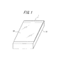
図1は、本発明の一実施の形態に係る電子機器の全体を示す斜視図である。本実施の形態に係る電子機器1は、外観上、筐体10と、可撓性のシート部材20とを備えている。筐体10は、例えば樹脂製のケースなどとして、ある程度の衝撃に耐えうる素材により構成するのが好適である。なお、図示の例では、筐体10を一つの筐体として示しているが、上部筐体と下部筐体とが一体に組み合わされて構成される場合もある。この場合、上部筐体と下部筐体との間は、例えばゴム製のパッキンを介した密閉構造にする等して、適当な防塵対策が施される。
FIG. 1 is a perspective view showing an entire electronic apparatus according to an embodiment of the present invention. The electronic device 1 according to the present embodiment includes a
図2(a)〜(c)は、図1に示した電子機器1の内部の概略構成を示す図であり、図2(a)は平面図、図2(b)は図2(a)のB−B線断面図、図2(c)は図2(a)のC−C線断面図である。筐体10は、その表面側に矩形状の開口部11を有し、この開口部11に位置してタッチパネル30が配置され、タッチパネル30の裏面側に、該裏面から離間して表示部40が配置され、さらに、表示部40の裏面側に、該裏面から離間して回路基板50が配置される。
2A to 2C are diagrams showing a schematic configuration inside the electronic apparatus 1 shown in FIG. 1, FIG. 2A being a plan view, and FIG. 2B being FIG. FIG. 2C is a cross-sectional view taken along the line BB in FIG. 2A. The
タッチパネル30は、例えば、抵抗膜方式、静電容量方式、光学式等の公知の方式の透明なものを用いることができる。また、タッチパネル30は、図2に示す例では長方形状となっているが、正方形状であってもよい。本明細書において「長方形状」、「正方形状」とは、各辺が直線である場合に限らず、円弧である場合も含むものである。
As the
タッチパネル30は、タッチパネル制御回路に接続されて、タッチパネル制御回路により表示部40に表示されたオブジェクトに対する操作者の指やスタイラスペン等(以下、単に「接触物」と総称する)によるタッチパネル30のタッチ面(表面)31に対する接触を検出するとともに、タッチ面31に対する接触物の接触の位置を検出する。なお、タッチパネル30が接触物による接触を検出する上で、接触物がタッチパネル30に物理的に触れることは必須ではない。例えば、タッチパネル30が光学式である場合は、タッチパネル30は当該タッチパネル30上の赤外線が接触物で遮られた位置を検出するため、接触物がタッチパネル30に触れることは不要である。
The
タッチパネル30のタッチ面31とは反対側の面(裏面)32で、図2(a)に仮想線で示す表示部40の表示領域41から外れた領域には、2個の振動部60が設けられている。本実施の形態では、2個の振動部60を、タッチパネル30の短辺側の近傍において、その短辺に沿う向きにほぼ並行に延在して、例えば両面テープや接着剤等によって固着して設けられている。
Two
振動部60は、所定の振動パターンによる振動を発生させることにより、タッチパネル30に接触している接触物に対して触感を呈示する。本実施の形態において、振動部60は、例えば圧電素子からなり、圧電素子駆動回路から供給される駆動信号に基づいて、長手方向に伸縮変位する。これにより、タッチパネル30を、駆動信号に応じた振動パターンで長辺側を節として湾曲振動させて、タッチ面31に接触している接触物に対して触感を呈示する。
The
表示部40は、例えば、液晶表示パネル(LCD)や有機EL表示パネル等を用いて構成される。表示部40は、表示制御回路による制御に従って、例えばキーのような押しボタンスイッチ(プッシュ式ボタンスイッチ)等のオブジェクトを画像で表示する。このオブジェクトは、タッチパネル30のタッチ面31上において接触すべき領域を操作者に示唆する画像である。また、押しボタンスイッチとは、操作者が入力の操作に用いるボタンやキー等(以下、単に「キー等」と総称する)である。なお、本明細書においては、表示関連の事項については、詳細な説明を省略する。
The
回路基板50は、上述したタッチパネル制御回路、圧電素子駆動回路および表示制御回路を含む電子機器1の動作に必要な回路を実装し、タッチパネル30、振動部60および表示部40とフレキシブル配線基板(FPC)等を介して接続される。また、筐体10に電源や映像等の外部入出力部が設けられる場合は、回路基板50に外部入出力部に対応する回路が実装されて、回路基板50と外部入出力部とがFPC等を介して接続される。
The
本実施の形態において、表示部40は、画像表示面(表面)42とは反対側の面(裏面)43が、筐体10の内壁12に形成された支持部13に支持される。支持部13は、筐体10の内壁12から、表示部40の裏面43側の周縁部の全周に亘って凸状に突出して形成されている。そして、表示部40は、その裏面43側の周縁部が、全周に亘って支持部13に固着されて支持される。なお、表示部40の支持部13への固着は、接着剤、両面テープ、ビス止め等の公知の態様が可能である。表示部40は、支持部13へ、例えば接着剤、両面テープ、ビス止め等により気密に支持されることにより、回路基板50から表示部40の表面側へ埃が侵入するおそれを低減することができる。なお、ここで、表示部40と支持部13との間の気密の度合いは、回路基板50側から表示部40の表面側へ埃が侵入するおそれを低減することができる程度の気密の度合いであればよく、気体が全く侵入しないような完全な気密の度合いである必要はない。
In the present embodiment, the
また、タッチパネル30は、筐体10の開口部11に位置して、振動部60により振動可能に、弾性支持部材70を介して表示部40の表面42に支持される。本実施の形態では、振動部60による振動の節となるタッチパネル30の各長辺部の裏面32において、表示部40の表示領域41から外れた両端部および中央部の3箇所、したがって両辺で合計6箇所を、それぞれ弾性支持部材70を介して、表示部40の表示領域41から外れた表面42に支持する。なお、筐体10の開口部11は、タッチパネル30の側面と筐体10との間に、タッチパネル30の振動に支障をきたさない程度の間隙14が、タッチパネル30の周縁に亘って形成される大きさとする。
In addition, the
また、シート部材20は、タッチパネル30の周縁の間隙14からの埃が侵入するおそれを低減するもので、間隙14を跨ってタッチパネル30の表面31および筐体10の表面15に、接着剤や両面テープ等を用いて接着して設けられる。なお、シート部材20は、間隙14を跨れば、必ずしもタッチパネル30の表面全体を覆う必要はないが、本実施の形態においては、タッチパネル30を傷等から保護するために、タッチパネル30の表面全体を覆うように設けている。したがって、本実施の形態において、シート部材20は、少なくとも、表示部40の表示領域41に対応する領域は、透明となっている。なお、シート部材20の厚さは、耐久性等に応じて適宜設定される。また、シート部材20は、例えばPET(ポリエチレンテレフタレート)等の可撓性材料により構成される。
In addition, the
回路基板50は、筐体10の底部16と表示部40との間、図示の例では、底部16と支持部13との間に配置される。なお、タッチパネル30や振動部60のFPCは、表示部40と支持部13との間を、両面テープ等を用いて気密に通して回路基板50に接続する。あるいは、支持部13の一部にFPCが貫通する開口を形成し、FPCを貫通させて回路基板50に接続した後、樹脂等により開口を閉塞する。あるいは、表示部40に中継コネクタを設けて、中継コネクタを介して回路基板50に接続する。
The
上記のように構成される本実施の形態における電子機器1は、表示部40にキー等を表示させることで、タッチパネル30を通してそのキー等が視認される。ここで、操作者が、接触物によって、キー等が視認される部位のタッチパネル30に触れると、振動部60が駆動されて、タッチパネル30が湾曲振動する。これにより、タッチパネル30に触れている接触物に対して、例えば押しボタンスイッチを押したような触感を呈示することができる。
The electronic device 1 according to the present embodiment configured as described above causes the keys and the like to be visually recognized through the
しかも、タッチパネル30の周縁と筐体10との間隙14は、可撓性を有するシート部材20で覆われており、表示部40は、その裏面43の周縁部が全周に亘って、筐体10の内壁12から突出して形成された支持部13に固着されている。したがって、タッチパネル30とその支持部材との間、本実施の形態では表示部40との間に、全周に亘って弾性部材を介在させる防塵構造と比較して、タッチパネル30の振動の減衰を抑制して、表示部40の画像表示面である表面42への防塵機能を十分に発揮させることができる。
In addition, the
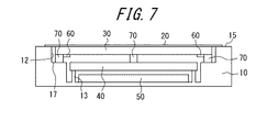
次に、上述した電子機器1の各種の変形例について、図3〜図7を参照して説明する。なお、図3〜図7は、図2(c)の断面図に相当するものであり、上述した構成要素と同様の作用をなす構成要素には、同一参照符号を付して説明を省略する。 Next, various modifications of the electronic device 1 described above will be described with reference to FIGS. 3 to 7 correspond to the cross-sectional view of FIG. 2 (c), and the same reference numerals are given to the constituent elements having the same functions as the constituent elements described above, and the description thereof will be omitted. .
図3に示す変形例は、表示部40の支持部13を、筐体10の内壁12から底部16に亘って段差状に突出して形成したものである。図4に示す変形例は、筐体10にタッチパネル30を支持する段差部17を形成し、この段差部17に弾性支持部材70を介してタッチパネル30を振動可能に支持したものである。図5に示す変形例は、図3に示した表示部40の支持構造と、図4に示したタッチパネル30の支持構造とを組み合わせたものである。
In the modification shown in FIG. 3, the
図6に示す変形例は、表示部40の支持部13を、筐体10の底部16から表示部40の裏面側周縁部の全周に亘って枠状に突出して、つまり底部16から立ち上げて形成し、その上面に表示部40を固着したものである。図7に示す変形例は、図6において、タッチパネル30の支持構造を図4および図5と同様の支持構造としたものである。なお、図6および図7において、回路基板50に接続される外部入出力部がある場合は、表示部40の表面42が位置する空間に、外部入出力部が連通しないように、外部入出力部のみを独立して防塵構造としたり、外部入出力部が回路基板50の位置する空間に存在するように支持部13を適宜変形したりすればよい。
In the modification shown in FIG. 6, the
図3〜図7の電子機器においても、図2に示した電子機器1と同様に、タッチパネル30の振動の減衰を抑制して、表示部40の画像表示面である表面42への防塵機能を十分に発揮させることができる。
3 to 7, similarly to the electronic device 1 shown in FIG. 2, the vibration attenuation of the
なお、本発明は、上記実施の形態や変形例に限定されるものではなく、更なる変形または変更が可能である。例えば、表示部40の支持部13は、必ずしも表示部40の裏面周縁部の全周に亘って設ける必要はなく、一部に例えばタッチパネル30や振動部60のFPCを通すための切り欠きがあってもよい。この場合は、例えば、表示部40の裏面43から閉塞用のシート状部材を延在させて、該シート状部材により当該切り欠きを閉塞するようにして、表示部40の裏面側周縁部が全周に亘って支持部13に対して気密に支持されるようにすればよい。
In addition, this invention is not limited to the said embodiment and modification, The further deformation | transformation or change is possible. For example, the
また、タッチパネル30を振動させる振動部60は、2個に限らず、所要の振動振幅に応じて任意の個数とすることができる。また、振動部60は、タッチパネル30の全面に透明圧電素子を設けて構成したり、振動モータ(偏心モータ)を用いて構成したり、することもできる。また、タッチパネル30を振動可能に支持する弾性支持部材70は、6個に限らず、タッチパネル30の大きさに応じて、4点支持や8点支持等、適宜変更可能である。また、タッチパネル30は、筐体10の開口部11の側面に振動可能に支持してもよい。
Further, the number of
さらに、タッチパネル30は、接触の位置を検出する構成に限らず、単に接触の有無を検出する構成であってもよい。また、タッチパネル30に、例えば、押圧を検出する押圧検出部をさらに設け、押圧検出部により検出される押圧に基づくデータが所定の基準を満たした際に、タッチパネル30に対する接触がなされたものと判定したり、振動部60を駆動して触感を提示したりすることができる。ここで、押圧に基づくデータが所定の基準を満たした際とは、押圧に基づくデータが基準値に達した際であってもよいし、押圧に基づくデータが基準値を超えた際でもよいし、基準値が検出された際でもよい。
Furthermore, the
このような押圧検出部は、例えば、タッチパネル30に任意の個数の歪みゲージセンサ等を設けて構成したり、振動部60を圧電素子で構成する場合は、当該圧電素子を共用して構成したりすることができる。あるいは、押圧検出部は、タッチパネル30による接触検出方式に応じて構成したりすることもできる。例えば、抵抗膜方式の場合は、接触面積による抵抗変化に基づく出力信号の変化から押圧に基づくデータを取得するように押圧検出部を構成したり、また、静電容量方式の場合は、静電容量の変化に基づく出力信号の変化から押圧に基づくデータを取得するように押圧検出部を構成したりすることができる。
For example, such a pressure detection unit is configured by providing an arbitrary number of strain gauge sensors or the like on the
1 電子機器
10 筐体
11 筐体の開口部
12 筐体の内壁
13 支持部
14 間隙
15 筐体の表面
16 筐体の底部
17 段差部
20 シート部材
30 タッチパネル
31 タッチパネルのタッチ面(表面)
32 タッチパネルの裏面
40 表示部
41 表示領域
42 表示部の画像表示面(表面)
43 表示部の裏面
50 回路基板
60 振動部
70 弾性支持部材
DESCRIPTION OF SYMBOLS 1
32 Rear surface of
43 Back surface of
Claims (3)
該タッチパネルを筐体の開口部に位置させて振動可能に支持する弾性支持部材と、
前記タッチパネルを振動させる振動部と、
前記タッチパネルの裏面側に、該裏面から離間して配置される表示部と、
該表示部の裏面側に、該裏面から離間して配置される回路基板と、
前記表示部の裏面側周縁部を支持するように前記筐体に形成された支持部と、を有し、
前記タッチパネルの表面および前記筐体の表面には、該タッチパネルの周縁と前記筐体との間隙に跨って可撓性のシート部材が設けられ、
前記表示部は、その裏面側周縁部が全周に亘って前記支持部に対して気密に支持されている、ことを特徴とする電子機器。A touch panel;
An elastic support member for supporting the touch panel so as to vibrate by being positioned at the opening of the housing;
A vibrating section for vibrating the touch panel;
A display unit disposed on the back side of the touch panel, spaced apart from the back side;
A circuit board disposed on the back side of the display unit and spaced from the back side;
A support portion formed on the housing so as to support a peripheral portion on the back surface side of the display portion,
On the surface of the touch panel and the surface of the housing, a flexible sheet member is provided across the gap between the periphery of the touch panel and the housing,
The display device is an electronic device characterized in that the back side peripheral edge thereof is airtightly supported with respect to the support part over the entire circumference.
The electronic device according to claim 1, wherein the support portion is formed to protrude in a frame shape from the bottom portion of the housing to the entire periphery of the rear surface side peripheral portion of the display portion.
Priority Applications (1)
| Application Number | Priority Date | Filing Date | Title |
|---|---|---|---|
| JP2013529869A JP5586787B2 (en) | 2011-08-19 | 2012-08-14 | Electronics |
Applications Claiming Priority (4)
| Application Number | Priority Date | Filing Date | Title |
|---|---|---|---|
| JP2011179821 | 2011-08-19 | ||
| JP2011179821 | 2011-08-19 | ||
| PCT/JP2012/005151 WO2013027374A1 (en) | 2011-08-19 | 2012-08-14 | Electronic apparatus |
| JP2013529869A JP5586787B2 (en) | 2011-08-19 | 2012-08-14 | Electronics |
Publications (2)
| Publication Number | Publication Date |
|---|---|
| JP5586787B2 true JP5586787B2 (en) | 2014-09-10 |
| JPWO2013027374A1 JPWO2013027374A1 (en) | 2015-03-05 |
Family
ID=47746143
Family Applications (1)
| Application Number | Title | Priority Date | Filing Date |
|---|---|---|---|
| JP2013529869A Active JP5586787B2 (en) | 2011-08-19 | 2012-08-14 | Electronics |
Country Status (3)
| Country | Link |
|---|---|
| US (1) | US9317122B2 (en) |
| JP (1) | JP5586787B2 (en) |
| WO (1) | WO2013027374A1 (en) |
Families Citing this family (7)
| Publication number | Priority date | Publication date | Assignee | Title |
|---|---|---|---|---|
| JP5687331B2 (en) * | 2011-02-24 | 2015-03-18 | 京セラ株式会社 | Waterproof electronic equipment |
| JP5610096B2 (en) * | 2011-12-27 | 2014-10-22 | 株式会社村田製作所 | Tactile presentation device |
| JP6194716B2 (en) * | 2013-09-19 | 2017-09-13 | 株式会社デンソーウェーブ | Remote controller |
| KR20160148881A (en) * | 2015-06-17 | 2016-12-27 | 에스프린팅솔루션 주식회사 | Image forming apparatus and electronic apparatus |
| JP6111315B1 (en) | 2015-11-27 | 2017-04-05 | 京セラ株式会社 | Tactile presentation device |
| US20170357322A1 (en) * | 2016-06-08 | 2017-12-14 | Mplus Co., Ltd. | Terminal device on which piezo actuator module using piezo has been installed |
| JP6818572B2 (en) * | 2017-01-31 | 2021-01-20 | 京セラ株式会社 | Touch panel and display device |
Citations (9)
| Publication number | Priority date | Publication date | Assignee | Title |
|---|---|---|---|---|
| JPH05143233A (en) * | 1991-11-25 | 1993-06-11 | Sharp Corp | Electronic apparatus with display function |
| JPH07231178A (en) * | 1994-02-18 | 1995-08-29 | Yoshiaki Iida | Water-proof and dust-proof structure of casing |
| JPH08130381A (en) * | 1994-10-31 | 1996-05-21 | Nec Corp | Dust-proof structure of electronic equipment provided with display |
| JP2005209868A (en) * | 2004-01-22 | 2005-08-04 | Casio Comput Co Ltd | Electronic apparatus |
| JP2007034736A (en) * | 2005-07-27 | 2007-02-08 | Sharp Corp | Display device with touch panel |
| JP2007293488A (en) * | 2006-04-24 | 2007-11-08 | Koyo Electronics Ind Co Ltd | Indicator |
| JP2007316861A (en) * | 2006-05-24 | 2007-12-06 | Sharp Corp | Sealing structure |
| JP2010282534A (en) * | 2009-06-08 | 2010-12-16 | Panasonic Corp | Touch panel and terminal device having the same |
| JP2011113461A (en) * | 2009-11-30 | 2011-06-09 | Smk Corp | Holding structure for touch panel |
Family Cites Families (12)
| Publication number | Priority date | Publication date | Assignee | Title |
|---|---|---|---|---|
| US6504713B1 (en) * | 1998-01-22 | 2003-01-07 | Iv Phoenix Group, Inc. | Ultra-rugged, high-performance computer system |
| US6751552B1 (en) * | 2002-06-28 | 2004-06-15 | Garmin Ltd. | Rugged, waterproof, navigation device with touch panel |
| JP4516852B2 (en) * | 2005-02-04 | 2010-08-04 | Necインフロンティア株式会社 | Electronics |
| US9007309B2 (en) * | 2007-04-05 | 2015-04-14 | Japan Display Inc. | Input device, and electro-optical device |
| JP2010044497A (en) | 2008-08-11 | 2010-02-25 | Sumitomo Wiring Syst Ltd | Frame for fixing panel, and display |
| DE102008058568A1 (en) * | 2008-11-21 | 2010-05-27 | Continental Automotive Gmbh | Haptic control device |
| JP4723656B2 (en) * | 2009-02-03 | 2011-07-13 | 京セラ株式会社 | Input device |
| KR20110023030A (en) * | 2009-08-28 | 2011-03-08 | 삼성전기주식회사 | Touch screen device |
| EP2325733B1 (en) * | 2009-11-02 | 2013-06-12 | SMK Corporation | Holding structure for a touch panel |
| EP2325731B1 (en) | 2009-11-02 | 2013-11-13 | SMK Corporation | Holding structure for a touch panel |
| JP4811965B2 (en) * | 2009-11-02 | 2011-11-09 | Smk株式会社 | Touch panel holding structure |
| JP2012027855A (en) * | 2010-07-27 | 2012-02-09 | Kyocera Corp | Tactile sense presentation device and control method of tactile sense presentation device |
-
2012
- 2012-08-14 WO PCT/JP2012/005151 patent/WO2013027374A1/en active Application Filing
- 2012-08-14 US US14/239,526 patent/US9317122B2/en active Active
- 2012-08-14 JP JP2013529869A patent/JP5586787B2/en active Active
Patent Citations (9)
| Publication number | Priority date | Publication date | Assignee | Title |
|---|---|---|---|---|
| JPH05143233A (en) * | 1991-11-25 | 1993-06-11 | Sharp Corp | Electronic apparatus with display function |
| JPH07231178A (en) * | 1994-02-18 | 1995-08-29 | Yoshiaki Iida | Water-proof and dust-proof structure of casing |
| JPH08130381A (en) * | 1994-10-31 | 1996-05-21 | Nec Corp | Dust-proof structure of electronic equipment provided with display |
| JP2005209868A (en) * | 2004-01-22 | 2005-08-04 | Casio Comput Co Ltd | Electronic apparatus |
| JP2007034736A (en) * | 2005-07-27 | 2007-02-08 | Sharp Corp | Display device with touch panel |
| JP2007293488A (en) * | 2006-04-24 | 2007-11-08 | Koyo Electronics Ind Co Ltd | Indicator |
| JP2007316861A (en) * | 2006-05-24 | 2007-12-06 | Sharp Corp | Sealing structure |
| JP2010282534A (en) * | 2009-06-08 | 2010-12-16 | Panasonic Corp | Touch panel and terminal device having the same |
| JP2011113461A (en) * | 2009-11-30 | 2011-06-09 | Smk Corp | Holding structure for touch panel |
Also Published As
| Publication number | Publication date |
|---|---|
| US20140176318A1 (en) | 2014-06-26 |
| US9317122B2 (en) | 2016-04-19 |
| WO2013027374A1 (en) | 2013-02-28 |
| JPWO2013027374A1 (en) | 2015-03-05 |
Similar Documents
| Publication | Publication Date | Title |
|---|---|---|
| WO2012114761A1 (en) | Electronic device | |
| JP5586787B2 (en) | Electronics | |
| JP5919025B2 (en) | Electronics | |
| JP2012190450A (en) | Electronic device | |
| JP2012190452A (en) | Electronic device | |
| JP5809081B2 (en) | Electronics | |
| JP5638634B2 (en) | Electronics | |
| JP5809080B2 (en) | Electronics | |
| JP5611078B2 (en) | Electronics | |
| JP2012173955A (en) | Electronic apparatus | |
| JP5767995B2 (en) | Electronics | |
| JP5777552B2 (en) | Electronics | |
| JP5805571B2 (en) | Electronics | |
| JP5719196B2 (en) | Electronics | |
| JP5530026B2 (en) | Electronics | |
| JP2012185815A (en) | Electronic device | |
| JP5496373B2 (en) | Electronics | |
| JP5731227B2 (en) | Electronics | |
| JP5606954B2 (en) | Electronics | |
| JP5715862B2 (en) | Electronics | |
| WO2012140878A1 (en) | Electronic device | |
| JP2012216141A (en) | Electronic device | |
| JP5921811B2 (en) | Electronics | |
| JP5665591B2 (en) | Electronics | |
| WO2012140877A1 (en) | Electronic device |
Legal Events
| Date | Code | Title | Description |
|---|---|---|---|
| TRDD | Decision of grant or rejection written | ||
| A01 | Written decision to grant a patent or to grant a registration (utility model) |
Free format text: JAPANESE INTERMEDIATE CODE: A01 Effective date: 20140624 |
|
| A61 | First payment of annual fees (during grant procedure) |
Free format text: JAPANESE INTERMEDIATE CODE: A61 Effective date: 20140722 |
|
| R150 | Certificate of patent or registration of utility model |
Ref document number: 5586787 Country of ref document: JP Free format text: JAPANESE INTERMEDIATE CODE: R150 |