JP5576480B2 - Vertical coplanar waveguide with tunable characteristic impedance, its design structure, and its fabrication method - Google Patents
Vertical coplanar waveguide with tunable characteristic impedance, its design structure, and its fabrication method Download PDFInfo
- Publication number
- JP5576480B2 JP5576480B2 JP2012513950A JP2012513950A JP5576480B2 JP 5576480 B2 JP5576480 B2 JP 5576480B2 JP 2012513950 A JP2012513950 A JP 2012513950A JP 2012513950 A JP2012513950 A JP 2012513950A JP 5576480 B2 JP5576480 B2 JP 5576480B2
- Authority
- JP
- Japan
- Prior art keywords
- line
- ground line
- signal line
- lower ground
- upper ground
- Prior art date
- Legal status (The legal status is an assumption and is not a legal conclusion. Google has not performed a legal analysis and makes no representation as to the accuracy of the status listed.)
- Expired - Fee Related
Links
Images


Classifications
-
- H—ELECTRICITY
- H01—ELECTRIC ELEMENTS
- H01P—WAVEGUIDES; RESONATORS, LINES, OR OTHER DEVICES OF THE WAVEGUIDE TYPE
- H01P3/00—Waveguides; Transmission lines of the waveguide type
- H01P3/003—Coplanar lines
-
- H—ELECTRICITY
- H01—ELECTRIC ELEMENTS
- H01P—WAVEGUIDES; RESONATORS, LINES, OR OTHER DEVICES OF THE WAVEGUIDE TYPE
- H01P3/00—Waveguides; Transmission lines of the waveguide type
- H01P3/02—Waveguides; Transmission lines of the waveguide type with two longitudinal conductors
- H01P3/08—Microstrips; Strip lines
- H01P3/085—Triplate lines
Description
本発明は、一般にオンチップ伝送線路に関し、さらに具体的には、整調可能な特性インピーダンスを有するオンチップ垂直型共平面導波路、その設計構造、およびその作製方法に関する。 The present invention generally relates to an on-chip transmission line, and more specifically to an on-chip vertical coplanar waveguide having a tunable characteristic impedance, a design structure thereof, and a manufacturing method thereof.
オンチップ伝送線路など、オンチップ相互接続のパフォーマンスは、全体的なチップのパフォーマンスに影響する重要なファクタである。設計時間を短縮するために、オンチップ伝送線路は、多くの場合生産開始の前にモデリングされる。オンチップ伝送線路は全体的なチップのパフォーマンスにとって重要であるが故に、高性能設計を評価する際には、オンチップ伝送線路の正確なモデルが必要である。伝送線路のモデルに何らかのエラーが存在すると、チップ中の該伝送線路に関連する特性インピーダンスもしくは減衰またはその両方の不正確な見積もりをもたらすことになる。誤ったモデリングに基づいて作られたチップは、設計仕様書で要求される仕方で機能できず、しかして、時間、労力および資本の使用が非効率となる。 The performance of on-chip interconnects, such as on-chip transmission lines, is an important factor that affects overall chip performance. To reduce design time, on-chip transmission lines are often modeled before production begins. Because on-chip transmission lines are important to overall chip performance, accurate models of on-chip transmission lines are required when evaluating high performance designs. Any error in the transmission line model will lead to an inaccurate estimate of the characteristic impedance and / or attenuation associated with the transmission line in the chip. A chip made based on incorrect modeling cannot function in the way required by the design specification, which results in inefficient use of time, effort and capital.
オンチップ伝送線路の一般的な型は、共平面導波路である。従来型の共平面導波路は、2本の接地ラインを両側に配置された一本の信号ラインを備える。全3本のライン、すなわち信号ラインおよび2本の接地ラインは、半導体構造体の共通の配線レベルに形成され、しかして、ほぼ水平な共平面にある。 A common type of on-chip transmission line is a coplanar waveguide. A conventional coplanar waveguide comprises a single signal line with two ground lines on either side. All three lines, namely the signal line and the two ground lines, are formed at a common wiring level of the semiconductor structure and are therefore in a substantially horizontal coplanar.
従来型のオンチップ共平面導波路は、共平面導波路の近辺の半導体構造体の非対称性によってモデリングの難しい非対称性電界が生ずるので、モデリングするのが難しい。従来型共平面導波路のモデリングの難しさは、電界が、例えば共平面導波路の上側で空気と交差したり、例えば共平面導波路の下側でシリコン基板と交差したりする場合、さらにその度合いを増す。これは、空気とのカップリングもしくは基板とのカップリングまたはその両方に対する高精度なモデルがないからである。その結果、ほとんどの設計者は、モデリングを用いるよりはむしろ、作製済みのプロトタイプのハードウエア測定に依存してチップ設計を検証するので、設計サイクルおよび製品のマーケティングの時間が遅延する。 Conventional on-chip coplanar waveguides are difficult to model because an asymmetry field that is difficult to model is generated by the asymmetry of the semiconductor structure in the vicinity of the coplanar waveguide. The difficulty in modeling conventional coplanar waveguides is further increased if the electric field crosses air, for example, above the coplanar waveguide, or crosses the silicon substrate, for example, below the coplanar waveguide. Increase the degree. This is because there is no highly accurate model for air coupling and / or substrate coupling. As a result, design cycles and product marketing time are delayed because most designers rely on the hardware measurements of fabricated prototypes rather than using modeling to validate chip designs.
そこで、前述の欠陥および制限を克服することが当該分野で求められている。 Thus, there is a need in the art to overcome the aforementioned deficiencies and limitations.
本発明の第一態様には、信号ライン、信号ラインの上側にあって該信号ラインから離間された上方接地ライン、および信号ラインの下側にあって該信号ラインから離間された下方接地ラインを包含する、オンチップ伝送線路がある。この信号ライン、上方接地ライン、および下方接地ラインは、誘電体材料中にほぼ垂直並びに配列されている。 The first aspect of the present invention includes a signal line, an upper ground line above the signal line and spaced from the signal line, and a lower ground line below the signal line and spaced from the signal line. Includes on-chip transmission lines. The signal line, upper ground line, and lower ground line are arranged substantially vertically and in the dielectric material.
本発明の別の態様には、半導体構造体を作製する方法がある。該方法は、能動デバイスの上側の少なくとも一つの配線レベル中にオンチップ伝送線路の下方接地ラインを形成するステップと、少なくとも一つの配線レベルの上側の第二配線レベル中にオンチップ伝送線路の信号ラインを形成するステップと、第二配線レベルの上側の第三配線レベルにオンチップ伝送線路の上方接地ラインを形成するステップとを含む。 Another aspect of the invention is a method for fabricating a semiconductor structure. The method includes forming a lower ground line of an on-chip transmission line in at least one wiring level above the active device, and a signal on the on-chip transmission line in a second wiring level above the at least one wiring level. Forming a line and forming an upper ground line of the on-chip transmission line at a third wiring level above the second wiring level.
本発明の別の態様には、集積回路を設計、製造、または試験するために用いるマシン可読媒体中に有形に具現された設計構造がある。設計構造は、信号ライン、信号ラインの上側にあって該信号ラインから離間された上方接地ライン、および信号ラインの下側にあって該信号ラインから離間された下方接地ラインを包含する。この信号ライン、上方接地ライン、および下方接地ラインは、誘電体材料中にほぼ垂直並びに配列されている。 Another aspect of the invention is a design structure tangibly embodied in a machine readable medium used to design, manufacture, or test an integrated circuit. The design structure includes a signal line, an upper ground line above the signal line and spaced from the signal line, and a lower ground line below the signal line and spaced from the signal line. The signal line, upper ground line, and lower ground line are arranged substantially vertically and in the dielectric material.
本発明を、言及された複数の図面を本発明の典型的実施形態の非限定の例として参照しながら、以下の詳細な記述で説明する。 The invention will be described in the following detailed description, with reference to the drawings referred to as non-limiting examples of exemplary embodiments of the invention.
本発明は、一般にオンチップ伝送線路に関し、さらに具体的には、整調可能な特性インピーダンスを有するオンチップ垂直型共平面導波路、その設計構造、およびその作製方法に関する。諸実施形態において、オンチップ伝送線路は、能動デバイス上方の配線レベル中に形成された信号ラインを含む。第一接地ラインは、信号ラインの下側の配線レベルに形成され、誘電体材料によって信号ラインから隔てられている。第二接地ラインは、信号ラインの上側の配線レベルに形成され、これも誘電体材料によって信号ラインから隔てられている。信号ラインおよび2本の接地ラインは誘電体材料中に垂直並びに配列され、垂直型共平面導波路に対してほぼ対称的な電界をもたらす。このような方法で、本発明の実装は正確にモデリングするのがより容易な設計構造を提供する。 The present invention generally relates to an on-chip transmission line, and more specifically to an on-chip vertical coplanar waveguide having a tunable characteristic impedance, a design structure thereof, and a manufacturing method thereof. In embodiments, the on-chip transmission line includes a signal line formed in a wiring level above the active device. The first ground line is formed at the lower wiring level of the signal line and is separated from the signal line by a dielectric material. The second ground line is formed at the wiring level above the signal line, which is also separated from the signal line by a dielectric material. The signal line and the two ground lines are aligned vertically in the dielectric material, resulting in a substantially symmetric electric field with respect to the vertical coplanar waveguide. In this way, the implementation of the present invention provides a design structure that is easier to model accurately.
本発明の態様によれば、垂直型共平面導波路の特性インピーダンスは整調可能で、例えば、信号ラインもしくは接地ラインまたはその両方の厚さ(例、水平方向の寸法)を変化させることによって調整することができる。本発明のさらなる態様によれば、垂直型共平面導波路の特性インピーダンスは、垂直型共平面導波路の長手沿いに、垂直型共平面導波路の両側に金属ストリップを形成することによって整調することができる。例えば、垂直型共平面導波路の特性インピーダンスは、垂直型共平面導波路と金属ストリップとの間の水平方向間隔、垂直型共平面導波路長手沿いの金属ストリップ間の間隔、垂直型共平面導波路長手沿いの金属ストリップの寸法、もしくは、金属ストリップを垂直型共平面導波路の接地ラインに対し浮遊させたり接続させたりすることによって、またはこれらの組み合わせによって変化させることができる。 In accordance with aspects of the present invention, the characteristic impedance of a vertical coplanar waveguide can be tuned, for example, by changing the thickness (eg, horizontal dimension) of a signal line and / or ground line. be able to. According to a further aspect of the invention, the characteristic impedance of the vertical coplanar waveguide is tuned by forming metal strips on both sides of the vertical coplanar waveguide along the length of the vertical coplanar waveguide. Can do. For example, the characteristic impedance of a vertical coplanar waveguide is the horizontal spacing between the vertical coplanar waveguide and the metal strip, the spacing between the metal strips along the length of the vertical coplanar waveguide, and the vertical coplanar waveguide. The size of the metal strip along the length of the waveguide, or the metal strip can be suspended or connected to the ground line of the vertical coplanar waveguide, or a combination thereof.
図1は、酸化物層25中に形成された、伝導性信号ライン10、および伝導性接地ライン15、20を包含する水平型共平面導波路5を示す。酸化物層25は、シリコン基板30の上に形成される。窒化物層35およびパッシベーション層40(例、ポリイミド)が、酸化物層25の上に形成される。パッシベーション層40の上面は、通常、空気45と連通している。矢印線「E」は、信号ライン10から発し接地ライン15、20で終端する電界を表す。
FIG. 1 shows a
図1に示されるように、水平型共平面導波路5の上方に存在する電界「E」は、水平型共平面導波路の下方に存在する電界「E」とは異なる材料の異なった層を通過する。さらに具体的には、水平型共平面導波路5の上部において、電界「E」は、酸化物層25の薄い部分と、窒化物層35と、パッシベーション層40と、空気45とを通過する。他方、水平型共平面導波路5の底部では、電界「E」は、酸化物層25の厚い部分およびシリコン基板30を通過する。水平型共平面導波路5を取り囲む材料中の非対称性は、モデリングすることが困難な非対称の電界「E」をもたらす。水平型共平面導波路5のモデリングの難しさは、電界「E」に対する空気45およびシリコン基板30の影響の正確なモデルの欠如によって、その度合いをさらに増す。
As shown in FIG. 1, the electric field “E” existing above the
また、図1に示された水平型共平面導波路5は、シリコン基板30と交差する電界「E」に起因するパフォーマンス上の不利も被る。CMOS技術において、電気的に信号ライン10および接地ライン15、20にカップリングしている低抵抗率のシリコン基板30の影響で、オンチップ伝送線路の挿入損失が増大する。かかる基板のカップリングに関連する損失誘起の特性は、水平型共平面導波路5のRFパフォーマンスに悪影響を与える。
The
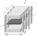
図2は、本発明の態様による垂直型共平面導波路60を示す。諸実施形態において、垂直型共平面導波路60は、誘電体材料80中に相互にほぼ垂直並びの配列で形成された、伝導性信号ライン65、伝導性上方接地ライン70、および伝導性下方接地ライン75を包含する。誘電体材料80は、能動デバイスのシリコン基板85上を覆って形成することができる。窒化物層90およびパッシベーション層95は、パッシベーション層95の上面を空気100に露出させて、酸化物層80の上に重ねて形成することができる。誘電体材料80には、以下に限らないが、high−k誘電体、low−k誘電体、超low−k誘電体、酸化物などを含めることができる。例えば、誘電体材料80には、ホウ燐ケイ酸ガラス(BPSG:borophosphosilicate glass)または高密プラズマ(HDP:high density plasma)酸化物を含めることができる。
FIG. 2 illustrates a
図2に示されるように、垂直型共平面導波路60の電界「E」は、完全にまたはほぼ完全に、単一種の材料、例えば誘電体材料80の内部に存在する。これは、垂直型共平面導波路60に対し、図1の水平型共平面導波路5に比べてより高い対称性の電界「E」をもたらす。しかして、垂直型共平面導波路60は、図1の水平型共平面導波路5に比べてモデリングし易い。
As shown in FIG. 2, the electric field “E” of the vertical
さらに図2を参照すると、誘電体材料80中の、信号ライン65、上方接地ライン70、および下方接地ライン75の垂直並び配列によって、垂直型共平面導波路60の電界「E」に対する空気100およびシリコン基板85の影響はほとんどない。しかして、垂直型共平面導波路60は、図1の水平型共平面導波路5と比べて、より正確にモデリングすることができる。さらに、本発明の態様による垂直型共平面導波路60では、電界が基本的には誘電体材料80内に包含されているので、基板のカップリングの影響は最小化される。かくして、垂直型共平面導波路60は、図1の水平型共平面導波路5よりも、より良好な損失特性を有する。
Still referring to FIG. 2, the vertical alignment of
図3は、本発明の態様による、垂直型共平面導波路60の両側の随意的な金属ストリップ110、115を示す。諸実施形態において、金属ストリップ110、115は、信号ライン65、上方接地ライン70、および下方接地ライン75の、左側および右側の誘電体材料80中に形成される。本明細書中でさらに詳しく説明するように、垂直型共平面導波路60の特性インピーダンスは、信号ライン65、上方接地ライン70、および下方接地ライン75の両側に金属ストリップ110、115を設けることによって、特定の所望の値に整調することができる。これらストリップは、接地レベル面(例、上方接地ライン70および下方接地ライン75)に直接接続することができ、あるいは浮遊させる(例えば、接地レベル面に直接接続しない)ことができる。また、垂直型共平面導波路60の特性インピーダンスは、信号ライン65、上方接地ライン70、および下方接地ライン75の厚さ「t」を変えることによっても整調することができる。
FIG. 3 illustrates
図4は、本発明の態様による、垂直並びに配列された信号ライン65、上方接地ライン70、および下方接地ライン75を含む垂直型共平面導波路60の透視図を示す。複数の金属ストリップ110、115が、垂直アレイの垂直型共平面導波路60の長手沿いに、垂直型共平面導波路60の左側および右側に配置されている。寸法「t」は、信号ライン65、上方接地ライン70、および下方接地ライン75の水平方向の厚さを表す。寸法「d」は、垂直型共平面導波路60と金属ストリップ110、115との間の水平方向の距離を表す。寸法「w」は、金属ストリップ110、115の幅を表し、寸法「s」は、水平および垂直方向に対し直交方向(例、垂直型共平面導波路60の長手沿い)の、金属ストリップ110、115間の間隔を表す。寸法「t」、「d」、「w」、および「s」は、下記で説明するいくつかの例示的な非限定の寸法を含め、特定のアプリケーションおよび設計に応じて変えることができる。
FIG. 4 illustrates a perspective view of a vertical
接地レベル面(例、上方および下方接地ライン70、75)と信号レベル面(例、信号ライン65)との間の静電容量は、「t」、「d」、「w」、および「s」寸法のいずれか一つ以上を変えることによって変化させることができる。特性インピーダンスは、Z0=SQRT(L/C)で定義され、「L」は単位長あたりのインダクタンスであり、「C」は単位長あたりの静電容量である。従って、垂直型共平面導波路60の特性インピーダンスは、「t」、「d」、「w」、および「s」寸法を適切に選択することによって整調することができる。このように、本発明の実装を用いて、約35オーム〜約75オームの範囲、望ましくは約50オームの特性インピーダンスを実現することができる。ただし、本発明はこれらの値に限定されるものでなく、「t」、「d」、「w」、および「s」寸法を調整することによって、任意の所望の特性インピーダンスを求めることができる。
The capacitance between the ground level plane (eg, upper and
本発明の態様によれば、図2〜4に図示された構造は、従来式の処理技術を用い、積層された半導体構造体として作製することができる。例えば、図5〜7は、本発明の態様による、伝送線路構造体を形成するための構造およびそれぞれの処理ステップを示す。具体的に、図5は、基板85およびその上に形成された誘電体層125を含む、例示的半導体構造体の断面を示す。基板85は、従来式の処理技術を用いて形成することができ、これには、例えば、半導体デバイス(例、ゲート、ソース/ドレイン領域など)が中に形成されるシリコン基板を包含させることができる。誘電体層125は、従来式のプロセスを用いて形成することができ、以下に限らないが、high−k誘電体、low−k誘電体、超low−k誘電体などを含め、任意の適切な材料で構成することができる。例えば、誘電体層125は、図2および3に関連して前述した誘電体材料80に相当する、任意の適切な酸化物材料を含めることができる。
According to aspects of the present invention, the structures illustrated in FIGS. 2-4 can be fabricated as stacked semiconductor structures using conventional processing techniques. For example, FIGS. 5-7 illustrate structures and respective processing steps for forming a transmission line structure in accordance with aspects of the present invention. Specifically, FIG. 5 shows a cross-section of an exemplary semiconductor structure that includes a
さらに図5を参照すると、誘電体層125の上に配線レベルM1が形成されている。諸実施形態において、配線レベルM1は、例えば酸化物材料など誘電体層125と同じ材料から成る。従来式のリソグラフィ・エッチングおよび堆積プロセスを用いて、配線レベルM1中に導体部分130が形成される。導体部分130は、以下に限らないが、銅、アルミニウム、合金類などを含め、任意の適切な伝導材料で構成することができ、従来式のプロセスを用いて形成することができる。
Still referring to FIG. 5, a wiring level M <b> 1 is formed on the
図6は、図5の構造体の上に、追加の配線レベルM2、M3、M4、およびMQ、並びにビア・レベルV1、V2、V3、およびVQが形成された構造体を示す。諸実施形態において、配線レベルM2〜MQおよびビア・レベルV1〜VQの全ては、例えば酸化物など、第一配線レベルM1と同じ材料から成る。さらに、各配線レベルM2〜MQおよびビア・レベルV1〜VQは、それぞれ、導体部分130と類似の導体部分を包含する。複数のそれぞれの導体部分は、図2〜4に関連して前述した下方接地ライン75を形成するように構築され配置される。このようにして、下方接地ライン75は、複数の配線レベルおよびビア・レベルに拡延する。
FIG. 6 shows a structure in which additional wiring levels M2, M3, M4, and MQ and via levels V1, V2, V3, and VQ are formed on the structure of FIG. In embodiments, the interconnect levels M2-MQ and the via levels V1-VQ are all made of the same material as the first interconnect level M1, such as an oxide. Further, each of the wiring levels M2 to MQ and the via levels V1 to VQ includes a conductor portion similar to the
図7は、図6の構造体の上に、M1〜MQレベルを覆って、追加の配線レベル135、LY、145、AM、および155が形成された構造体を示す。諸実施形態において、配線レベル135、LY、145、AM、および155の全ては、例えば酸化物など、配線レベルM1〜MQと同じ材料から成る。本発明の態様によれば、信号ライン65は、配線レベルLY中に形成され、上方接地ライン70は配線レベルAM中に形成される。信号ライン65および上方接地ライン70は、以下に限らないが、銅、アルミニウム、合金類などを含め、任意の適切な伝導性材料で作製することができ、従来式のプロセスを用いて形成することができる。
FIG. 7 shows a structure in which
図5〜7のフィーチャは、標準的な配線形成(BEOL:back end of line)プロセスなど、従来式の技術を用いて形成することができる。例えば、これらのフィーチャは、以下に限らないが、フォトリソグラフィ・マスキングおよび露光、エッチング(例、反応性イオン・エッチング(RIE:reactive ion etching)など)、メタライゼーション(例、化学気相堆積(CVD:chemical vapor deposition)など)、および平坦化・研磨プロセス(例、化学機械研磨(CMP:chemical mechanical polishing)など)を包含する、製造プロセスを用いて形成することができる。加えて、図5〜7に示されていないさらなるフィーチャを、本発明の実装に用いることができる。例えば、バリヤ材を、ライナ、キャップなどとして用いることができる。 The features of FIGS. 5-7 can be formed using conventional techniques, such as a standard end-of-line (BEOL) process. For example, these features include, but are not limited to, photolithography masking and exposure, etching (eg, reactive ion etching (RIE), etc.), metallization (eg, chemical vapor deposition (CVD) : Chemical vapor deposition), and planarization / polishing processes (eg, chemical mechanical polishing (CMP), etc.). In addition, additional features not shown in FIGS. 5-7 can be used to implement the present invention. For example, a barrier material can be used as a liner, a cap, or the like.
さらに、図5〜7に示された各種のレベルは、任意の適切な高さにすることができ、相互に異なった高さとすることができる。例えば、配線レベルM1〜MQを合わせて約3.56μmの高さとし、レベル135を約4μmの高さとし、レベルLYを約1.25μmの高さとし、レベル145を約4μmの高さとし、レベルAMを約4μmの高さとすることができる。ただし、本発明はこれらの値に限定されるものでなく、任意の適切な高さを用いることができる。さらに、本発明は、図示した配線レベルの数には限定されない。それどころか、本発明の態様は、任意の数の配線レベルを有する半導体デバイス(例、アナログ・デバイス、デジタル・デバイスなど)に使うことができる。
Further, the various levels shown in FIGS. 5-7 can be any suitable height and can be different from each other. For example, the wiring levels M1 to MQ are about 3.56 .mu.m, the
さらになお、上方接地ライン70、下方接地ライン75、および信号ライン65は、任意の適切な厚さ「t」にすることができる。図3および7の図示では、上方接地ライン70、下方接地ライン75、および信号ライン65の全ては同じ厚さ「t」を有する。しかしながら、本発明は、この構成に限定されるものでなく、代わりに、上方接地ライン70、下方接地ライン75、および信号ライン65各々をそれぞれ異なる厚さ「t」にすることができる。さらに、上方接地ライン70、および信号ライン65は、それぞれ単一の配線レベルに限定されるものでなく、複数の配線レベルに拡延することができる(存在する場合、ビア・レベルについても同様)。同様に、下方接地ライン75が複数のレベルM1〜MQにまたがって示されているが、かかる実装に限定されるものでなく、それどころか、単一のレベルで遜色なく形成することができる。
Still further, the
図5〜7には示されていないが、金属ストリップ110および115は、図5〜7に示された積層半導体構造体のレベル群中の、上方接地ライン70、下方接地ライン75、および信号ライン65と、実質上同時に形成することができる。すなわち、金属ストリップ110および115に対応する伝導性材料は、従来式プロセスを用いて、選択された配線レベルおよびビア・レベル中の選択された位置に形成することができる。配線レベル内の選択された位置に金属ストリップ110および115を形成することによって、(図4に関連して前述した)「d」、「w」、および「s」寸法を任意の所望のやり方で調整することができる。図4に関連して前述したように、接地レベル面(例、上方および下方接地ライン70、75)と信号レベル面(例、信号ライン65)との間の静電容量は、「t」、「d」、「w」、および「s」寸法の任意の一つ以上を変更することによって変化させることができる。従って、垂直型共平面導波路60の特性インピーダンスは、図5〜7に関連する処理ステップの過程で、「t」、「d」、「w」、および「s」寸法を適切に選択することによって整調することができる。本発明の態様によれば、寸法「t」、「d」、「w」、および「s」に対し、任意の所望値を選択することができる。
Although not shown in FIGS. 5-7, the metal strips 110 and 115 are upper ground lines 70,
図8は、水平型共平面導波路と本発明の態様による垂直型共平面導波路との間での挿入損失値の比較を示す。カーブ200は、LY層に形成され、1.52μmの幅を有する水平型共平面導波路の挿入損失を表す。カーブ205は、図5〜7に従って形成され、1.25μmの「t」寸法を有する垂直型共平面導波路を表す。図8に示されるように、垂直型共平面導波路は、水平型共平面導波路よりも小さな挿入損失を示す。
FIG. 8 shows a comparison of insertion loss values between a horizontal coplanar waveguide and a vertical coplanar waveguide according to aspects of the present invention.
図9は、本発明の態様によって形成された垂直型共平面導波路に対する特性インピーダンスの値の比較を示す。4つのカーブ220、225、230、235は、図5〜7に従って形成され、金属ストリップ(例、エレメント110、115)を一切有せず、それぞれ、1.25μm、4μm、5μm、および10μmの「t」寸法を有する、垂直型共平面導波路にそれぞれ対応している。図9に示されるように、特性インピーダンスは、「t」寸法が増すにつれて低減する。
FIG. 9 shows a comparison of characteristic impedance values for a vertical coplanar waveguide formed in accordance with aspects of the present invention. The four
図10は、本発明の態様によって形成された垂直型共平面導波路の特性インピーダンスの値の比較を示す。3つのカーブ250、255、および260は、それぞれ、図5〜7に従って形成され、各々5μmの「t」寸法を有する垂直型共平面導波路に対応する。カーブ250は、金属ストリップ(例、110、115)を持たない垂直型共平面導波路に対応する。カーブ255は、「d」が1.0μmに等しく「s」が0に等しい浮遊金属ストリップを有する垂直型共平面導波路に対応する。カーブ260は、「d」が0.5μmに等しく「w」が2μmに等しく「s」が2μmに等しい金属ストリップを有する垂直型共平面導波路に対応する。図10に示されたデータは、金属ストリップの使用がインピーダンスに影響を与えることを明示している。
FIG. 10 shows a comparison of characteristic impedance values of vertical coplanar waveguides formed according to aspects of the present invention. The three
図11は、本発明の態様によって形成された垂直型共平面導波路の、単位長あたりの静電容量の比較を示す。4つのカーブ270、275、280、285は、それぞれ、図5〜7に従って形成され、各々10μmの「t」寸法を有する垂直型共平面導波路に対応する。カーブ270は、金属ストリップ(例、110、115)を持たない垂直型共平面導波路に対応する。カーブ275は、「d」が1.0μmに等しく「s」が0に等しい浮遊金属ストリップを有する(例えば、金属ストリップが、垂直型共平面導波路の長手沿いに走る固体プレートである)垂直型共平面導波路に対応する。カーブ280および285は、各々、「d」が0.5μmに等しく「w」が2μmに等しく「s」が2μmに等しい金属ストリップを有する垂直型共平面導波路に対応する。カーブ280は、金属ストリップが垂直型共平面導波路に直接接続されていない(例えば、金属ストリップが浮遊している)構造に対応し、カーブ285は、金属ストリップが接地レベル面に直接接続されている(例えば、ストリップ110および115が上方および下方接地ライン70、75に直接接続されている)構造に対応する。
FIG. 11 shows a comparison of capacitance per unit length for vertical coplanar waveguides formed according to aspects of the present invention. The four
図12は、図11に示された静電容量値に対応する特性インピーダンスの値の比較を示す。さらに具体的には、カーブ270’、275’、280’、および285’は、それぞれ、カーブ270、275、280、および285に対応するインピーダンスを表す。図11および図12に図示されたデータは、金属ストリップが静電容量に、従ってインピーダンスに影響を与えることを明示している。
FIG. 12 shows a comparison of characteristic impedance values corresponding to the capacitance values shown in FIG. More specifically, curves 270 ', 275', 280 ', and 285' represent impedances corresponding to
図13は、本発明の態様によって形成された垂直型共平面導波路に対する特性インピーダンスの値の比較を示す。4つのカーブ300、305、310、および315は、それぞれ、図5〜7に従って形成され、各々15μmの「t」寸法を有する垂直型共平面導波路に対応する。カーブ300は、金属ストリップ(例、110、115)を持たない垂直型共平面導波路に対応する。カーブ305、310、および315は、「d」が0.5μmに等しく「w」が2μmに等しく、異なった「s」寸法を持つ浮遊金属ストリップ、を有する垂直型共平面導波路に対応する。具体的には、カーブ305に対する「s」は1μmに等しく、カーブ310に対する「s」は2μmに等しく、カーブ315に対する「s」は5μmに等しい。図13に示されたデータは、金属ストリップ間の間隔がインピーダンスに影響を与えることを明示している。
FIG. 13 shows a comparison of characteristic impedance values for a vertical coplanar waveguide formed according to aspects of the present invention. The four
既に説明したように、本発明の態様によって形成された垂直型共平面導波路は、基板損失の低減によって、従来型の水平型共平面導波路に比べてより良好な挿入損失を有する。加えて、この垂直型共平面導波路は、垂直型共平面導波路に関連する電界の対称性の故に、水平型共平面導波路よりもモデリングがし易い。さらに、垂直型共平面導波路の特性インピーダンスは、信号ラインおよび接地ラインの厚さ(例、「t」寸法)を変えることによって広範囲に整調することができる。また、特性インピーダンスは、信号ラインおよび接地ライン沿いに金属ストリップを加えることによって、さらに、金属ストリップに関連する「d」、「s」、および「w」寸法を適切に選択することによって整調することができる。 As already explained, vertical coplanar waveguides formed in accordance with aspects of the present invention have better insertion loss than conventional horizontal coplanar waveguides due to reduced substrate loss. In addition, this vertical coplanar waveguide is easier to model than a horizontal coplanar waveguide because of the symmetry of the electric field associated with the vertical coplanar waveguide. Furthermore, the characteristic impedance of a vertical coplanar waveguide can be tuned over a wide range by changing the thickness of the signal and ground lines (eg, the “t” dimension). Also, the characteristic impedance is tuned by adding metal strips along the signal and ground lines and by appropriately selecting the “d”, “s”, and “w” dimensions associated with the metal strip. Can do.
図14は、例えば半導体ICロジックの設計、シミュレーション、試験、レイアウト、および製造に用いられる、例示的設計フロー900のブロック図を示す。設計フロー900は、前述し図2〜7で示した設計構造もしくはデバイスまたはその両方と論理的にまたは別途機能的に等しい表現を生成するための、設計構造またはデバイスを処理するプロセス、マシン、もしくはメカニズムまたはこれらの組み合わせを包含する。設計フロー900によって処理もしくは生成されまたはその両方が行われる設計構造については、マシン可読の送信媒体または記憶媒体上に符号化して、データ処理システムで実行または別途処理されたときに、ハードウエア・コンポーネント、回路、デバイス、またはシステムと論理的に、構造的に、機械的にまたは別途機能的に等しい表現を生成する、データもしくは命令またはその両方を包含させることができる。マシンは、以下に限らないが、回路、コンポーネント、デバイス、またはシステムの設計、製造、またはシミュレーションなど、IC設計プロセスで用いられる任意のマシンを包含する。例えば、マシンは、リソグラフィ・マシン、マスクを生成するためのマシンもしくは設備またはその両方(例、電子ビーム・ライタ)、設計構造をシミュレーティングするためのコンピュータまたは設備、製造または試験プロセスで使われる任意の装置、または設計構造と機能的に等しい表現を任意の媒体中にプログラミングするための任意のマシン(例、プログラム可能ゲート・アレイをプログラミングするためのマシン)を包含し得る。
FIG. 14 shows a block diagram of an
設計フロー900は、設計される表現の種類によって変わり得る。例えば、特定用途向けIC(ASIC:application specific IC)の作製のための設計フロー900は、標準コンポーネント設計のための設計フロー900、あるいは、設計を、例えば、Altera(R) Inc.またはXilinx(R) Inc.によって提供されるプログラム可能ゲート・アレイ(PGA:programmable gate array)またはフィールド・プログラム可能ゲート・アレイ(FPGA:field programmable gate array)などのプログラム可能アレイの中にインスタンス化するための設計フロー900とは異なり得る。
The
図14は、望ましくは設計プロセス910によって処理されるインプット設計構造920を含め、かかる複数の設計構造を示す。設計構造920は、設計プロセス910によって生成、処理されて、ハードウエア・デバイスと論理的に等しい機能的表現を生成する論理シミュレーション設計構造とすることができる。設計構造920には、さらにあるいは上記に換えて、設計プロセス910によって処理されたときハードウエア・デバイスの物理的構造の機能的表現を生成する、データもしくはプログラム命令、またはその両方を含めることができる。機能的なもしくは構造的な設計特質またはその両方の現出を行うかどうかにかかわらず、設計構造920は、例えばコア開発者/設計者によって実装された、電子的コンピュータ支援設計(ECAD:electronic computer−aided design)を用いて生成することができる。設計構造920は、マシン可読のデータ送信、ゲート・アレイ、または記憶媒体に符号化された場合、設計プロセス910内の一つ以上のハードウエア・モジュールもしくはソフトウエア・モジュールまたはこれらの両方によって、アクセスされて処理され、図2〜7に示されるような、電子コンポーネント、回路、電子または論理モジュール、装置、デバイス、またはシステムをシミュレートするか、または別途機能的に現出させることができる。しかして、設計構造920には、設計またはシミュレーション・データ処理システムで処理されたとき、ハードウエア論理設計の回路または他のレベルを機能的にシミュレートまたは別途現出させる、人間可読もしくはマシン可読またはその両方のソース・コード、コンパイル済み構造、および、コンピュータ実行可能コード構造を包含する、ファイルまたは他のデータ構造を含めることができる。かかるデータ構造には、Verilog(R)およびVHDLなどの低レベルのHDL設計言語もしくはCまたはC++などのより高度なレベルの設計言語またはその両方に適合するもしくはこれらと両立するまたはその両方の、ハードウエア記述言語(HDL:hardware−description language)設計エンティティまたは他のデータ構造を包含させることができる。
FIG. 14 illustrates such a plurality of design structures, including an
設計プロセス910は、望ましくは、図2〜7に示されたコンポーネント、回路、デバイス、または論理構造の設計/シミュレーションの機能的同等物を合成、変換、または別途に処理し、設計構造920などの設計構造を包含可能なネットリスト980を生成するための、ハードウエア・モジュールもしくはソフトウエア・モジュールまたはその両方を使用しこれらを組み込む。ネットリスト980には、例えば、集積回路設計中の他のエレメントおよび回路への接続を記載した、配線、個別コンポーネント、論理ゲート、制御回路、I/Oデバイス、モデルなどのリストを表す、コンパイル済みのまたは別途処理されたデータ構造を含めることができる。ネットリスト980は、デバイスに対する設計仕様およびパラメータに応じ、ネットリスト980が一回以上再編成される反復プロセスを使って編成される。ネットリスト980は、本明細書に記載する他の設計構造の種類とともに、マシン可読データ記憶媒体に記録、またはプログラム可能ゲート・アレイにプログラムすることができる。この媒体は、磁気または光ディスク・ドライブなどの不揮発性記憶媒体、プログラム可能ゲート・アレイ、コンパクト・フラッシュ、または他のフラッシュ・メモリとすることができる。追加または代替として、該媒体は、システムまたはキャッシュ・メモリ、バッファ・スペースとしてもよいし、データ・パケットをインターネットを介して送信し、中間で格納することが可能な電気的または光学的伝導性デバイスおよび材料としてもよいし、あるいは他のネットワーク利用に適した手段としてもよい。
The
設計プロセス910には、ネットリスト980を含むさまざまな入力データ構造の種類を処理するための、ハードウエアおよびソフトウエア・モジュールを包含させることができる。かかるデータ構造の種類は、例えばライブラリ・エレメント930内に在置し、これに、所与の製造技術(例、各種技術ノード、32nm、45nm、90nmなど)のための、モデル、レイアウト、および記号的表現を含めて、一連のよく使われるエレメント、回路、およびデバイスを包含させることができる。これらデータ構造の種類には、設計仕様940と、特性設定データ950と、検証データ960と、設計ルール970、インプット試験パターン、アウトプット試験結果および他の試験情報を含めればよい試験データ・ファイル985とをさらに包含させることができる。設計プロセス910には、例えば、ストレス解析、熱解析、機械的事象シミュレーション、鋳込み、モールド、および金型プレス形成などの作業に対する工程シミュレーションなどの標準的な機械設計プロセスをさらに包含させることができる。機械的設計の当業者は、本発明の範囲および思想から逸脱することなく、設計プロセス910において用いることが可能な機械設計ツールおよびアプリケーションの範囲は十分理解できよう。また、設計プロセス910には、タイミング解析、検証、設計ルール・チェック、配置配線オペレーションなど、標準の回路設計プロセスを遂行するためのモジュールを包含させることができる。
The
設計プロセス910は、任意の追加的機械設計またはデータ(適用される場合)に加え、図示のサポート・データ構造の一部または全てと一緒に、設計構造920を処理して第二設計構造990を生成するための、HDLコンパイラおよびシミュレーション・モデル構築ツールなどのロジックおよび物理的設計のツールを使用し組み込む。設計構造990は、機械的デバイスおよび構造のデータの交換に使われるデータ・フォーマット(例、IGES、DXF、Parasolid(R)XT、JT、DRGによって、またはかかる機械的設計構造を格納またはレンダリングするために適した他の任意のフォーマットによって格納された情報)で、記憶媒体またはプログラム可能ゲート・アレイに在置される。設計構造990は、望ましくは設計構造920と同様に、送信またはデータ記憶媒体上に在置されていて、ECADシステムによって処理されたとき、図2〜7に示された本発明の実施形態の一つ以上と論理的にまたは別途機能的に同等な形態を生成する、一つ以上のファイル、データ構造、あるいは他のコンピュータ符号化のデータまたは命令を含む。一つの実施形態において、設計構造990には、図2〜7に示されたデバイスを機能的にシミュレートする、コンパイル済みの実行可能なHDLシミュレーション・モデルを含めることができる。
The
また、設計構造990は、集積回路のレイアウト・データの交換に使われるデータ・フォーマットもしくは記号的データ・フォーマット(例、GDSII(GDS2)、GL1、OASIS(R)、マップ・ファイル、または、かかる設計データ構造を格納するために適した他の任意のフォーマット)またはその両方を用いることができる。設計構造990には、例えば、記号的データ、マップ・ファイル、試験データ・ファイル、設計コンテント・ファイル、製造データ、レイアウト・パラメータ、配線、金属のレベル、ビア、形状、製造ラインを回送するデータ、および、前述し図2〜7に示したデバイスまたは構造を産生するため、製造者または他の設計者/開発者によって必要とされる任意の他のデータなどの情報を含めることができる。次いで、設計構造990は、ステージ995に進み、そこでは、例えば、設計構造990はテープアウトに進み、製造にリリースされたり、マスク事業所にリリースされたり、別の設計事業所に送付されたり、顧客に送り返されたりする。
The
前述の方法は、集積回路チップの作製に用いられる。得られた集積回路チップは、作製者によって、ベア・ダイとして生ウエハの形(すなわち、複数の未パッケージ・チップを有する単一のウエハ)で、またはパッケージされた形で流通させることができる。後者の場合、チップは、(マザーボードまたは他のより高次レベルのキャリヤに取り付けるためのリードを有するプラスチック・キャリヤなどの)単一チップ・パッケージ中に、または(表面相互接続または埋め込み相互接続のいずれかまたは両方を有するセラミック・キャリヤなどの)マルチ・チップ・パッケージ中に搭載される。いずれの場合でも、次いでチップは、(a)マザーボードなどの中間製品または(b)最終製品のいずれかの一部として、他のチップ、個別回路エレメント、もしくは他の信号処理デバイス、またはこれらの組み合わせとともに統合される。最終製品は、玩具および他のローエンド・アプリケーションから、ディスプレイ、キーボード、または他の入力デバイス、および中央処理装置を有する高度なコンピュータ製品に至るまでの、集積回路チップを包含する任意の製品であり得る。 The method described above is used to fabricate integrated circuit chips. The resulting integrated circuit chip can be distributed by the manufacturer as a bare die in the form of a raw wafer (ie, a single wafer having a plurality of unpackaged chips) or in a packaged form. In the latter case, the chip is either in a single chip package (such as a plastic carrier with leads for attachment to a motherboard or other higher level carrier) or either (surface or embedded interconnect) Or in a multi-chip package (such as a ceramic carrier having both). In any case, the chip then becomes another part, individual circuit element, or other signal processing device, or a combination thereof, as part of either (a) an intermediate product such as a motherboard or (b) an end product. Integrated with. The final product can be any product that includes integrated circuit chips, ranging from toys and other low-end applications to advanced computer products with displays, keyboards or other input devices, and central processing units. .
本明細書で用いられる用語は、特定の実施形態を説明する目的だけのためのものであり、本発明を限定することは意図していない。本明細書で用いられる、単数形「ある(a、an)」、および「前記、該(the)」は、文脈上明確に示されているものを除き、複数形も同じように含むことが意図されている。さらに、本明細書で用いられる「含む(comprise)」もしくは「含んでいる(comprising)」またはその両方は、述べられた機能、完全体、ステップ、オペレーション、エレメント、もしくはコンポーネント、またはこれらの組み合わせの存在を特定するが、一つ以上の他の機能、完全体、ステップ、オペレーション、エレメント、コンポーネント、もしくはこれらの群またはこれらの組み合わせの存在または追加を排除するものではない。 The terminology used herein is for the purpose of describing particular embodiments only and is not intended to be limiting of the invention. As used herein, the singular forms “a”, “an”, and “the” include the plural as well, unless the context clearly dictates otherwise. Is intended. Further, as used herein, “comprise” or “comprising” or both refers to the described function, completeness, step, operation, element, or component, or combinations thereof Identifying the presence does not exclude the presence or addition of one or more other functions, completeness, steps, operations, elements, components, or groups or combinations thereof.
添付の請求項中の全ての手段またはステップ・プラス・ファンクション・エレメントに対応する構造、材料、処置および同等物が、適用できる場合、それらには、明確に請求されている他の請求エレメントと組み合わせて該機能を遂行するための、一切の構造、材料、または処置を含めることが意図されている。本発明の記述は、例示および説明目的で提示されたもので、網羅的であることも、本発明を開示した形態に限定することも意図されていない。当業者には、本発明の範囲および思想から逸脱しない多くの変更および変形が明らかであろう。これら実施形態は、本発明の原理および実際的な応用を最善に説明し、他の当業者が、意図する特定の用途に適したさまざまな変更を加えたさまざまな実施形態のため、本発明を理解できるように選択し説明したものである。従って、本発明を実施形態に関連させて説明してきたが、当業者は、添付の請求項の思想および範囲内において、各種変更を用いて本発明を実施できることを認識していよう。 Where applicable, structures, materials, treatments and equivalents corresponding to all means or step-plus-function elements in the appended claims may be combined with other claimed elements specifically claimed. It is intended to include any structure, material, or procedure for performing the function. The description of the present invention has been presented for purposes of illustration and description, and is not intended to be exhaustive or limited to the invention in the form disclosed. Many modifications and variations will be apparent to those skilled in the art without departing from the scope and spirit of the invention. These embodiments best illustrate the principles and practical applications of the invention, and others skilled in the art will appreciate the invention for various embodiments with various modifications suitable for the particular application intended. It is chosen and explained so that it can be understood. Thus, while the invention has been described in connection with the embodiments, those skilled in the art will recognize that the invention can be practiced with various modifications within the spirit and scope of the appended claims.
Claims (11)
前記信号ラインの上側にあって前記信号ラインから離間された上方接地ラインと、
前記信号ラインの下側にあって前記信号ラインから離間された下方接地ラインと、
を含むオンチップ伝送線路であって、
前記信号ライン、前記上方接地ラインおよび前記下方接地ラインは、誘電体材料中に垂直並びに配列され、同一の水平方向厚さを有し、
前記信号ライン、前記上方接地ラインおよび前記下方接地ラインは、チップのそれぞれ異なった配線レベルに配置され、
前記信号ライン、前記上方接地ライン、および前記下方接地ラインの第一側に離間されて隣接する、該信号ライン、該上方接地ライン、および該下方接地ラインが配列する垂直方向へ延びる少なくとも一つの金属ストリップと、前記信号ライン、前記上方接地ライン、および前記下方接地ラインの第二側に離間されて隣接する、前記垂直方向へ延びる少なくとも一つの他の金属ストリップとをさらに含み、前記第一側は前記第二側に対向している、
オンチップ伝送線路。 A signal line;
An upper ground line above the signal line and spaced from the signal line;
A lower ground line below the signal line and spaced from the signal line;
Including an on-chip transmission line,
The signal line, the upper ground line and the lower ground line are arranged vertically and in a dielectric material and have the same horizontal thickness;
The signal line, the upper ground line, and the lower ground line are disposed at different wiring levels of the chip,
At least one metal extending in the vertical direction in which the signal line, the upper ground line, and the lower ground line are arranged adjacent to each other on the first side of the signal line, the upper ground line, and the lower ground line. Further comprising: a strip; and at least one other metal strip extending in the vertical direction spaced apart and adjacent to a second side of the signal line, the upper ground line, and the lower ground line; Facing the second side,
On-chip transmission line.
前記少なくとも一つの他の金属ストリップは、前記信号ライン、前記上方接地ラインおよび前記下方接地ラインの長手沿いの第二側から離間された第二の複数の金属ストリップを含む、
請求項1に記載のオンチップ伝送線路。 The at least one metal strip includes a first plurality of metal strips spaced from a first side along a length of the signal line, the upper ground line, and the lower ground line;
The at least one other metal strip includes a second plurality of metal strips spaced from a second side along a length of the signal line, the upper ground line, and the lower ground line;
The on-chip transmission line according to claim 1 .
(i)前記信号ライン、前記上方接地ライン、および前記下方接地ラインの前記第一側と、(ii)前記第一の複数の金属ストリップとの間の距離、
(i)前記信号ライン、前記上方接地ライン、および前記下方接地ラインの前記第二側と、(ii)前記第二の複数の金属ストリップとの間の距離、
前記第一の複数の金属ストリップおよび第二の複数の金属ストリップの各個の幅、および
前記第一の複数の金属ストリップおよび第二の複数の金属ストリップの各個の間隔の少なくとも一つは、前記伝送線路の特性インピーダンスが35オーム〜75オームの範囲になるように設定される、
請求項4に記載のオンチップ伝送線路。 The thickness of the signal line, the upper ground line, and the lower ground line;
(I) a distance between the first side of the signal line, the upper ground line, and the lower ground line and (ii) the first plurality of metal strips;
(Ii) a distance between the second side of the signal line, the upper ground line, and the lower ground line; and (ii) the second plurality of metal strips;
At least one of the width of each of the first plurality of metal strips and the second plurality of metal strips and the spacing of each of the first plurality of metal strips and the second plurality of metal strips is the transmission The characteristic impedance of the line is set to be in the range of 35 ohms to 75 ohms,
The on-chip transmission line according to claim 4 .
前記信号ラインの上側にあって前記信号ラインから離間された上方接地ラインと、
前記信号ラインの下側にあって前記信号ラインから離間された下方接地ラインと、
を含むオンチップ伝送線路であって、
前記信号ライン、前記上方接地ラインおよび前記下方接地ラインは、誘電体材料中に垂直並びに配列され、同一の水平方向厚さを有し、
前記信号ライン、前記上方接地ライン、および前記下方接地ラインの第一側から離間されて隣接する、該信号ライン、該上方接地ライン、および該下方接地ラインが配列する垂直方向へ延びる少なくとも一つの金属ストリップと、前記信号ライン、前記上方接地ライン、および前記下方接地ラインの第二側から離間されて隣接する、前記垂直方向へ延びる少なくとも一つの他の金属ストリップとをさらに含み、前記第一側は前記第二側に対向していて、
前記下方接地ラインは、複数の配線レベルに広がっており、
前記信号ライン、前記上方接地ラインおよび前記下方接地ラインは、それぞれ単一または複数の配線レベルに含まれており、
前記下方接地ラインは3.56μmの高さを有し、
前記信号ラインは1.25μmの高さを有し、
前記上方接地ラインは4μmの高さを有する、
オンチップ伝送線路。 A signal line;
An upper ground line above the signal line and spaced from the signal line;
A lower ground line below the signal line and spaced from the signal line;
Including an on-chip transmission line,
The signal line, the upper ground line and the lower ground line are arranged vertically and in a dielectric material and have the same horizontal thickness;
At least one metal extending in the vertical direction in which the signal line, the upper ground line, and the lower ground line are arranged adjacent to and spaced apart from the first side of the signal line, the upper ground line, and the lower ground line Further comprising: a strip; and at least one other metal strip extending in the vertical direction adjacent to and spaced from the second side of the signal line, the upper ground line, and the lower ground line, the first side comprising: Facing the second side,
The lower ground line extends to a plurality of wiring levels;
The signal line , the upper ground line, and the lower ground line are each included in a single or a plurality of wiring levels,
The lower ground line has a height of 3.56 μm;
The signal line has a height of 1.25 μm;
The upper ground line has a height of 4 μm;
On-chip transmission line.
能動デバイスの上側の少なくとも一つの配線レベル中にオンチップ伝送線路の下方接地ラインを形成するステップと、
前記少なくとも一つの配線レベルの上側の第二配線レベル中に前記オンチップ伝送線路の信号ラインを形成するステップと、
前記第二配線レベルの上側の第三配線レベル中に前記オンチップ伝送線路の上方接地ラインを形成するステップとを含み、
前記オンチップ伝送線路は、単一の型の材料内に形成された垂直な共平面の導波路を含み、
前記共平面の導波路の電界は、前記単一の型の材料内で相補的か、または略相補的とされ、
前記方法は、さらに、前記信号ライン、前記上方接地ライン、および前記下方接地ラインの第一側から離間されて隣接する、該信号ライン、該上方接地ライン、および該下方接地ラインが配列する垂直方向へ延びる第一の複数の金属ストリップを形成するステップと、前記信号ライン、前記上方接地ライン、および前記下方接地ラインの第二側から離間されて隣接する、前記垂直方向へ延びる第二の複数の金属ストリップを形成するステップとを含み、前記下方接地ライン、信号ライン、および上方接地ラインは、垂直並びに形成され、同一の水平方向厚さを有し、前記第一側は前記第二側と対向している、方法。 A method for fabricating a semiconductor structure comprising:
Forming a lower ground line of the on-chip transmission line in at least one wiring level above the active device;
Forming a signal line of the on-chip transmission line in a second wiring level above the at least one wiring level;
Forming an upper ground line of the on-chip transmission line in a third wiring level above the second wiring level;
The on-chip transmission line includes a vertical coplanar waveguide formed in a single type of material;
The electric field of the coplanar waveguide is complementary or substantially complementary within the single type of material;
The method further includes a vertical direction in which the signal line, the upper ground line, and the lower ground line are arranged adjacent to each other and spaced apart from the first side of the signal line, the upper ground line, and the lower ground line. Forming a first plurality of metal strips extending to , and a second plurality of vertically extending, spaced apart and adjacent to a second side of the signal line, the upper ground line, and the lower ground line Forming a metal strip, wherein the lower ground line, the signal line, and the upper ground line are formed vertically and have the same horizontal thickness, and the first side faces the second side The way you are.
能動デバイスの上側の少なくとも一つの配線レベル中にオンチップ伝送線路の下方接地ラインを形成するステップと、
前記少なくとも一つの配線レベルの上側の第二配線レベル中に前記オンチップ伝送線路の信号ラインを形成するステップと、
前記第二配線レベルの上側の第三配線レベル中に前記オンチップ伝送線路の上方接地ラインを形成するステップとを含み、
前記少なくとも一つの配線レベルは、複数の配線レベルおよび複数のビア・レベルとして形成され、
前記下方接地ラインを形成する前記ステップは、前記複数の配線レベルおよび前記複数のビア・レベルの各々の中に導体材料を配置するステップを含み、
前記方法は、さらに、前記信号ライン、前記上方接地ライン、および前記下方接地ラインの第一側に離間されて隣接する、該信号ライン、該上方接地ライン、および該下方接地ラインが配列する垂直方向へ延びる第一の複数の金属ストリップを形成するステップと、前記信号ライン、前記上方接地ライン、および前記下方接地ラインの第二側に離間されて隣接する、前記垂直方向へ延びる第二の複数の金属ストリップを形成するステップとを含み、前記下方接地ライン、信号ライン、および上方接地ラインは、垂直並びに形成され、同一の水平方向厚さを有し、前記第一側は前記第二側と対向している、方法。 A method for fabricating a semiconductor structure comprising:
Forming a lower ground line of the on-chip transmission line in at least one wiring level above the active device;
Forming a signal line of the on-chip transmission line in a second wiring level above the at least one wiring level;
Forming an upper ground line of the on-chip transmission line in a third wiring level above the second wiring level;
The at least one wiring level is formed as a plurality of wiring levels and a plurality of via levels;
The step of forming the lower ground line includes disposing a conductive material within each of the plurality of wiring levels and the plurality of via levels;
The method further includes a vertical direction in which the signal line, the upper ground line, and the lower ground line are arranged adjacent to each other on the first side of the signal line, the upper ground line, and the lower ground line. Forming a first plurality of metal strips extending to the signal line, the upper ground line, and a second plurality of the vertically extending second adjacent to the second side of the lower ground line. Forming a metal strip, wherein the lower ground line, the signal line, and the upper ground line are formed vertically and have the same horizontal thickness, and the first side faces the second side The way you are.
(i)前記信号ライン、前記上方接地ライン、および前記下方接地ラインの前記第一側と、(ii)前記第一の複数の金属ストリップとの間の距離、
(i)前記信号ライン、前記上方接地ライン、および前記下方接地ラインの前記第二側と、(ii)前記第二の複数の金属ストリップとの間の距離、
前記第一の複数の金属ストリップおよび第二の複数の金属ストリップの各個の幅、および
前記第一の複数の金属ストリップおよび第二の複数の金属ストリップの各個の間隔の少なくとも一つを調整することによって、前記伝送線路の特性インピーダンスを35オーム〜75オームの範囲内に整調するステップをさらに含む、請求項10に記載の方法 The thickness of the signal line, the upper ground line, and the lower ground line;
(I) a distance between the first side of the signal line, the upper ground line, and the lower ground line and (ii) the first plurality of metal strips;
(Ii) a distance between the second side of the signal line, the upper ground line, and the lower ground line; and (ii) the second plurality of metal strips;
Adjusting at least one of the width of each of the first plurality of metal strips and the second plurality of metal strips and the spacing of each of the first plurality of metal strips and the second plurality of metal strips; 11. The method of claim 10 , further comprising: tuning the characteristic impedance of the transmission line to within a range of 35 ohms to 75 ohms.
Applications Claiming Priority (3)
| Application Number | Priority Date | Filing Date | Title |
|---|---|---|---|
| US12/478,385 | 2009-06-04 | ||
| US12/478,385 US8212634B2 (en) | 2009-06-04 | 2009-06-04 | Vertical coplanar waveguide with tunable characteristic impedance design structure and method of fabricating the same |
| PCT/US2010/032645 WO2010141167A2 (en) | 2009-06-04 | 2010-04-28 | Vertical coplanar waveguide with tunable characteristic impedance, design structure and method of fabricating the same |
Publications (3)
| Publication Number | Publication Date |
|---|---|
| JP2012529226A JP2012529226A (en) | 2012-11-15 |
| JP2012529226A5 JP2012529226A5 (en) | 2013-10-03 |
| JP5576480B2 true JP5576480B2 (en) | 2014-08-20 |
Family
ID=43298387
Family Applications (1)
| Application Number | Title | Priority Date | Filing Date |
|---|---|---|---|
| JP2012513950A Expired - Fee Related JP5576480B2 (en) | 2009-06-04 | 2010-04-28 | Vertical coplanar waveguide with tunable characteristic impedance, its design structure, and its fabrication method |
Country Status (7)
| Country | Link |
|---|---|
| US (1) | US8212634B2 (en) |
| EP (1) | EP2438644A4 (en) |
| JP (1) | JP5576480B2 (en) |
| CN (1) | CN102428603B (en) |
| CA (1) | CA2757501A1 (en) |
| TW (1) | TWI513093B (en) |
| WO (1) | WO2010141167A2 (en) |
Families Citing this family (7)
| Publication number | Priority date | Publication date | Assignee | Title |
|---|---|---|---|---|
| US8994456B2 (en) | 2012-01-30 | 2015-03-31 | International Business Machines Corporation | Multi-stage amplifier using tunable transmission lines and frequency response calibration of same |
| US9362606B2 (en) | 2013-08-23 | 2016-06-07 | International Business Machines Corporation | On-chip vertical three dimensional microstrip line with characteristic impedance tuning technique and design structures |
| US9851506B2 (en) | 2015-06-04 | 2017-12-26 | Elenion Technologies, Llc | Back end of line process integrated optical device fabrication |
| US9588298B2 (en) * | 2015-06-04 | 2017-03-07 | Elenion Technologies, Llc | Edge coupler |
| TWI690043B (en) | 2016-02-17 | 2020-04-01 | 瑞昱半導體股份有限公司 | Integrated circuit device |
| DE102019126433A1 (en) * | 2019-03-14 | 2020-09-17 | Taiwan Semiconductor Manufacturing Company, Ltd. | Transmission line structures for millimeter wave signals |
| US11515609B2 (en) * | 2019-03-14 | 2022-11-29 | Taiwan Semiconductor Manufacturing Company, Ltd. | Transmission line structures for millimeter wave signals |
Family Cites Families (26)
| Publication number | Priority date | Publication date | Assignee | Title |
|---|---|---|---|---|
| US2812501A (en) * | 1954-03-04 | 1957-11-05 | Sanders Associates Inc | Transmission line |
| JP3362535B2 (en) | 1994-12-14 | 2003-01-07 | 株式会社村田製作所 | High frequency electromagnetic field coupling type thin film laminated electrode, high frequency transmission line, high frequency resonator, high frequency filter, high frequency device, and method of setting film thickness of high frequency electromagnetic field coupling type thin film laminated electrode |
| US5561405A (en) * | 1995-06-05 | 1996-10-01 | Hughes Aircraft Company | Vertical grounded coplanar waveguide H-bend interconnection apparatus |
| JP3307212B2 (en) * | 1996-02-13 | 2002-07-24 | 株式会社村田製作所 | Transmission line |
| US6353189B1 (en) * | 1997-04-16 | 2002-03-05 | Kabushiki Kaisha Toshiba | Wiring board, wiring board fabrication method, and semiconductor package |
| KR100287646B1 (en) | 1998-07-27 | 2001-04-16 | 김병규 | Microwave device with strip line structure and manufacturing method thereof |
| EP0977263A3 (en) * | 1998-07-31 | 2002-07-10 | STMicroelectronics, Inc. | Apparatus and method for reducing propagation delay in a conductor |
| JP3255118B2 (en) * | 1998-08-04 | 2002-02-12 | 株式会社村田製作所 | Transmission line and transmission line resonator |
| SE514406C2 (en) * | 1999-06-17 | 2001-02-19 | Ericsson Telefon Ab L M | Electric transmission device with intersecting stripline lines |
| JP2001006941A (en) | 1999-06-18 | 2001-01-12 | Fujitsu General Ltd | High frequency transformer and impedance converter |
| US7554829B2 (en) * | 1999-07-30 | 2009-06-30 | Micron Technology, Inc. | Transmission lines for CMOS integrated circuits |
| US6975189B1 (en) * | 2000-11-02 | 2005-12-13 | Telasic Communications, Inc. | On-chip multilayer metal shielded transmission line |
| JP2003234606A (en) * | 2002-02-07 | 2003-08-22 | Nippon Telegr & Teleph Corp <Ntt> | Microwave transmission line |
| US6759923B1 (en) * | 2002-02-19 | 2004-07-06 | Raytheon Company | Device for directing energy, and a method of making same |
| TW200409153A (en) * | 2002-09-04 | 2004-06-01 | Nec Corp | Strip line element, printed circuit board carrying member, circuit board, semiconductor package and method for forming same |
| US6832029B2 (en) * | 2002-12-17 | 2004-12-14 | Mcnc | Impedance control devices for use in the transition regions of electromagnetic and optical circuitry and methods for using the same |
| US6847273B2 (en) * | 2003-04-25 | 2005-01-25 | Cyntec Co., Ltd. | Miniaturized multi-layer coplanar wave guide low pass filter |
| US7504587B2 (en) * | 2003-08-29 | 2009-03-17 | Semiconductor Technology Academic Research Center | Parallel wiring and integrated circuit |
| US20050062137A1 (en) * | 2003-09-18 | 2005-03-24 | International Business Machines Corporation | Vertically-stacked co-planar transmission line structure for IC design |
| JP3982511B2 (en) * | 2004-03-09 | 2007-09-26 | ソニー株式会社 | Flat cable manufacturing method |
| US7103488B2 (en) * | 2004-07-16 | 2006-09-05 | International Business Machines Corporation | Method for determining fringing capacitances on passive devices within an integrated circuit |
| US7292449B2 (en) * | 2004-12-13 | 2007-11-06 | Lexmark International, Inc. | Virtual ground return for reduction of radiated emissions |
| JP4336319B2 (en) | 2005-02-24 | 2009-09-30 | 京セラ株式会社 | Multilayer stripline filter |
| DE102005033306B3 (en) * | 2005-07-16 | 2006-08-03 | Atmel Germany Gmbh | Monolithic integrated circuit for use as FlexRay (RTM) transceiver, has interference suppressing device for reducing interference radiation, and comprising strip conductor with section whose length is selected based on radiation frequency |
| WO2007044436A2 (en) * | 2005-10-05 | 2007-04-19 | Massachusetts Institute Of Technology | Ultra-high-q surface-tension-induced monolithically integrated on-chip resonator and associated devices |
| US7612638B2 (en) * | 2006-07-14 | 2009-11-03 | Taiwan Semiconductor Manufacturing Co., Ltd. | Waveguides in integrated circuits |
-
2009
- 2009-06-04 US US12/478,385 patent/US8212634B2/en not_active Expired - Fee Related
-
2010
- 2010-04-28 CA CA2757501A patent/CA2757501A1/en active Pending
- 2010-04-28 JP JP2012513950A patent/JP5576480B2/en not_active Expired - Fee Related
- 2010-04-28 WO PCT/US2010/032645 patent/WO2010141167A2/en active Application Filing
- 2010-04-28 EP EP10783756A patent/EP2438644A4/en not_active Withdrawn
- 2010-04-28 CN CN201080021236.3A patent/CN102428603B/en active Active
- 2010-06-01 TW TW099117559A patent/TWI513093B/en active
Also Published As
| Publication number | Publication date |
|---|---|
| EP2438644A4 (en) | 2013-01-23 |
| CA2757501A1 (en) | 2010-12-09 |
| TWI513093B (en) | 2015-12-11 |
| CN102428603A (en) | 2012-04-25 |
| EP2438644A2 (en) | 2012-04-11 |
| WO2010141167A3 (en) | 2011-01-27 |
| WO2010141167A2 (en) | 2010-12-09 |
| TW201123605A (en) | 2011-07-01 |
| CN102428603B (en) | 2014-01-22 |
| JP2012529226A (en) | 2012-11-15 |
| US20100315181A1 (en) | 2010-12-16 |
| US8212634B2 (en) | 2012-07-03 |
Similar Documents
| Publication | Publication Date | Title |
|---|---|---|
| JP5613244B2 (en) | Method, structure and design structure for feedthrough Wilkinson power divider | |
| JP5576480B2 (en) | Vertical coplanar waveguide with tunable characteristic impedance, its design structure, and its fabrication method | |
| US9035719B2 (en) | Three dimensional branchline coupler using through silicon vias and design structures | |
| US10712498B2 (en) | Shielding structures between optical waveguides | |
| KR101137060B1 (en) | Millimeter wave transmission line for slow phase velocity | |
| US20080079114A1 (en) | Striped on-chip inductor | |
| US8842412B2 (en) | Tapered via and MIM capacitor | |
| US8680689B1 (en) | Coplanar waveguide for stacked multi-chip systems | |
| US8916463B2 (en) | Wire bond splash containment | |
| US9553348B2 (en) | On-chip vertical three dimensional microstrip line with characteristic impedance tuning technique and design structures | |
| JP5567658B2 (en) | On-chip slow wave structure, manufacturing method and design structure thereof | |
| US9263782B2 (en) | Notch filter structure with open stubs in semiconductor substrate and design structure | |
| US8822993B2 (en) | Integrated circuit including sensor structure, related method and design structure | |
| US9443767B2 (en) | Structure for metal oxide semiconductor capacitor | |
| US8815733B2 (en) | Isolated wire structures with reduced stress, methods of manufacturing and design structures |
Legal Events
| Date | Code | Title | Description |
|---|---|---|---|
| A621 | Written request for application examination |
Free format text: JAPANESE INTERMEDIATE CODE: A621 Effective date: 20130116 |
|
| RD12 | Notification of acceptance of power of sub attorney |
Free format text: JAPANESE INTERMEDIATE CODE: A7432 Effective date: 20130731 |
|
| A521 | Request for written amendment filed |
Free format text: JAPANESE INTERMEDIATE CODE: A523 Effective date: 20130808 |
|
| A871 | Explanation of circumstances concerning accelerated examination |
Free format text: JAPANESE INTERMEDIATE CODE: A871 Effective date: 20130808 |
|
| A521 | Request for written amendment filed |
Free format text: JAPANESE INTERMEDIATE CODE: A821 Effective date: 20130731 |
|
| A977 | Report on retrieval |
Free format text: JAPANESE INTERMEDIATE CODE: A971007 Effective date: 20130911 |
|
| A131 | Notification of reasons for refusal |
Free format text: JAPANESE INTERMEDIATE CODE: A131 Effective date: 20130924 |
|
| A975 | Report on accelerated examination |
Free format text: JAPANESE INTERMEDIATE CODE: A971005 Effective date: 20131024 |
|
| A521 | Request for written amendment filed |
Free format text: JAPANESE INTERMEDIATE CODE: A523 Effective date: 20131030 |
|
| A02 | Decision of refusal |
Free format text: JAPANESE INTERMEDIATE CODE: A02 Effective date: 20131203 |
|
| A521 | Request for written amendment filed |
Free format text: JAPANESE INTERMEDIATE CODE: A523 Effective date: 20140327 |
|
| A911 | Transfer to examiner for re-examination before appeal (zenchi) |
Free format text: JAPANESE INTERMEDIATE CODE: A911 Effective date: 20140404 |
|
| TRDD | Decision of grant or rejection written | ||
| A01 | Written decision to grant a patent or to grant a registration (utility model) |
Free format text: JAPANESE INTERMEDIATE CODE: A01 Effective date: 20140617 |
|
| RD14 | Notification of resignation of power of sub attorney |
Free format text: JAPANESE INTERMEDIATE CODE: A7434 Effective date: 20140617 |
|
| A61 | First payment of annual fees (during grant procedure) |
Free format text: JAPANESE INTERMEDIATE CODE: A61 Effective date: 20140703 |
|
| R150 | Certificate of patent or registration of utility model |
Ref document number: 5576480 Country of ref document: JP Free format text: JAPANESE INTERMEDIATE CODE: R150 |
|
| R250 | Receipt of annual fees |
Free format text: JAPANESE INTERMEDIATE CODE: R250 |
|
| LAPS | Cancellation because of no payment of annual fees |