JP5554059B2 - Improved display device - Google Patents
Improved display device Download PDFInfo
- Publication number
- JP5554059B2 JP5554059B2 JP2009524263A JP2009524263A JP5554059B2 JP 5554059 B2 JP5554059 B2 JP 5554059B2 JP 2009524263 A JP2009524263 A JP 2009524263A JP 2009524263 A JP2009524263 A JP 2009524263A JP 5554059 B2 JP5554059 B2 JP 5554059B2
- Authority
- JP
- Japan
- Prior art keywords
- pixel
- electrode
- particles
- pixels
- addressing
- Prior art date
- Legal status (The legal status is an assumption and is not a legal conclusion. Google has not performed a legal analysis and makes no representation as to the accuracy of the status listed.)
- Expired - Fee Related
Links
- 239000002245 particle Substances 0.000 claims abstract description 163
- 230000003287 optical effect Effects 0.000 claims abstract description 38
- 238000000034 method Methods 0.000 claims abstract description 31
- 102100022769 POC1 centriolar protein homolog B Human genes 0.000 abstract description 15
- 101710125069 POC1 centriolar protein homolog B Proteins 0.000 abstract description 15
- 102100022778 POC1 centriolar protein homolog A Human genes 0.000 abstract description 11
- 101710125073 POC1 centriolar protein homolog A Proteins 0.000 abstract description 11
- 230000005684 electric field Effects 0.000 description 12
- 239000000758 substrate Substances 0.000 description 10
- 238000010586 diagram Methods 0.000 description 6
- 238000001962 electrophoresis Methods 0.000 description 2
- 230000000694 effects Effects 0.000 description 1
- 239000012530 fluid Substances 0.000 description 1
- 239000007788 liquid Substances 0.000 description 1
- 239000011159 matrix material Substances 0.000 description 1
- 239000007787 solid Substances 0.000 description 1
- 239000010409 thin film Substances 0.000 description 1
Images


Classifications
-
- G—PHYSICS
- G02—OPTICS
- G02F—OPTICAL DEVICES OR ARRANGEMENTS FOR THE CONTROL OF LIGHT BY MODIFICATION OF THE OPTICAL PROPERTIES OF THE MEDIA OF THE ELEMENTS INVOLVED THEREIN; NON-LINEAR OPTICS; FREQUENCY-CHANGING OF LIGHT; OPTICAL LOGIC ELEMENTS; OPTICAL ANALOGUE/DIGITAL CONVERTERS
- G02F1/00—Devices or arrangements for the control of the intensity, colour, phase, polarisation or direction of light arriving from an independent light source, e.g. switching, gating or modulating; Non-linear optics
- G02F1/01—Devices or arrangements for the control of the intensity, colour, phase, polarisation or direction of light arriving from an independent light source, e.g. switching, gating or modulating; Non-linear optics for the control of the intensity, phase, polarisation or colour
- G02F1/165—Devices or arrangements for the control of the intensity, colour, phase, polarisation or direction of light arriving from an independent light source, e.g. switching, gating or modulating; Non-linear optics for the control of the intensity, phase, polarisation or colour based on translational movement of particles in a fluid under the influence of an applied field
- G02F1/166—Devices or arrangements for the control of the intensity, colour, phase, polarisation or direction of light arriving from an independent light source, e.g. switching, gating or modulating; Non-linear optics for the control of the intensity, phase, polarisation or colour based on translational movement of particles in a fluid under the influence of an applied field characterised by the electro-optical or magneto-optical effect
- G02F1/167—Devices or arrangements for the control of the intensity, colour, phase, polarisation or direction of light arriving from an independent light source, e.g. switching, gating or modulating; Non-linear optics for the control of the intensity, phase, polarisation or colour based on translational movement of particles in a fluid under the influence of an applied field characterised by the electro-optical or magneto-optical effect by electrophoresis
-
- G—PHYSICS
- G09—EDUCATION; CRYPTOGRAPHY; DISPLAY; ADVERTISING; SEALS
- G09G—ARRANGEMENTS OR CIRCUITS FOR CONTROL OF INDICATING DEVICES USING STATIC MEANS TO PRESENT VARIABLE INFORMATION
- G09G3/00—Control arrangements or circuits, of interest only in connection with visual indicators other than cathode-ray tubes
- G09G3/20—Control arrangements or circuits, of interest only in connection with visual indicators other than cathode-ray tubes for presentation of an assembly of a number of characters, e.g. a page, by composing the assembly by combination of individual elements arranged in a matrix no fixed position being assigned to or needed to be assigned to the individual characters or partial characters
- G09G3/34—Control arrangements or circuits, of interest only in connection with visual indicators other than cathode-ray tubes for presentation of an assembly of a number of characters, e.g. a page, by composing the assembly by combination of individual elements arranged in a matrix no fixed position being assigned to or needed to be assigned to the individual characters or partial characters by control of light from an independent source
- G09G3/3433—Control arrangements or circuits, of interest only in connection with visual indicators other than cathode-ray tubes for presentation of an assembly of a number of characters, e.g. a page, by composing the assembly by combination of individual elements arranged in a matrix no fixed position being assigned to or needed to be assigned to the individual characters or partial characters by control of light from an independent source using light modulating elements actuated by an electric field and being other than liquid crystal devices and electrochromic devices
- G09G3/344—Control arrangements or circuits, of interest only in connection with visual indicators other than cathode-ray tubes for presentation of an assembly of a number of characters, e.g. a page, by composing the assembly by combination of individual elements arranged in a matrix no fixed position being assigned to or needed to be assigned to the individual characters or partial characters by control of light from an independent source using light modulating elements actuated by an electric field and being other than liquid crystal devices and electrochromic devices based on particles moving in a fluid or in a gas, e.g. electrophoretic devices
- G09G3/3446—Control arrangements or circuits, of interest only in connection with visual indicators other than cathode-ray tubes for presentation of an assembly of a number of characters, e.g. a page, by composing the assembly by combination of individual elements arranged in a matrix no fixed position being assigned to or needed to be assigned to the individual characters or partial characters by control of light from an independent source using light modulating elements actuated by an electric field and being other than liquid crystal devices and electrochromic devices based on particles moving in a fluid or in a gas, e.g. electrophoretic devices with more than two electrodes controlling the modulating element
-
- G—PHYSICS
- G02—OPTICS
- G02F—OPTICAL DEVICES OR ARRANGEMENTS FOR THE CONTROL OF LIGHT BY MODIFICATION OF THE OPTICAL PROPERTIES OF THE MEDIA OF THE ELEMENTS INVOLVED THEREIN; NON-LINEAR OPTICS; FREQUENCY-CHANGING OF LIGHT; OPTICAL LOGIC ELEMENTS; OPTICAL ANALOGUE/DIGITAL CONVERTERS
- G02F1/00—Devices or arrangements for the control of the intensity, colour, phase, polarisation or direction of light arriving from an independent light source, e.g. switching, gating or modulating; Non-linear optics
- G02F1/01—Devices or arrangements for the control of the intensity, colour, phase, polarisation or direction of light arriving from an independent light source, e.g. switching, gating or modulating; Non-linear optics for the control of the intensity, phase, polarisation or colour
- G02F1/13—Devices or arrangements for the control of the intensity, colour, phase, polarisation or direction of light arriving from an independent light source, e.g. switching, gating or modulating; Non-linear optics for the control of the intensity, phase, polarisation or colour based on liquid crystals, e.g. single liquid crystal display cells
- G02F1/133—Constructional arrangements; Operation of liquid crystal cells; Circuit arrangements
- G02F1/1333—Constructional arrangements; Manufacturing methods
- G02F1/1343—Electrodes
- G02F1/134309—Electrodes characterised by their geometrical arrangement
- G02F1/134363—Electrodes characterised by their geometrical arrangement for applying an electric field parallel to the substrate, i.e. in-plane switching [IPS]
-
- G—PHYSICS
- G02—OPTICS
- G02F—OPTICAL DEVICES OR ARRANGEMENTS FOR THE CONTROL OF LIGHT BY MODIFICATION OF THE OPTICAL PROPERTIES OF THE MEDIA OF THE ELEMENTS INVOLVED THEREIN; NON-LINEAR OPTICS; FREQUENCY-CHANGING OF LIGHT; OPTICAL LOGIC ELEMENTS; OPTICAL ANALOGUE/DIGITAL CONVERTERS
- G02F1/00—Devices or arrangements for the control of the intensity, colour, phase, polarisation or direction of light arriving from an independent light source, e.g. switching, gating or modulating; Non-linear optics
- G02F1/01—Devices or arrangements for the control of the intensity, colour, phase, polarisation or direction of light arriving from an independent light source, e.g. switching, gating or modulating; Non-linear optics for the control of the intensity, phase, polarisation or colour
- G02F1/165—Devices or arrangements for the control of the intensity, colour, phase, polarisation or direction of light arriving from an independent light source, e.g. switching, gating or modulating; Non-linear optics for the control of the intensity, phase, polarisation or colour based on translational movement of particles in a fluid under the influence of an applied field
- G02F1/1675—Constructional details
- G02F1/1677—Structural association of cells with optical devices, e.g. reflectors or illuminating devices
-
- G—PHYSICS
- G09—EDUCATION; CRYPTOGRAPHY; DISPLAY; ADVERTISING; SEALS
- G09G—ARRANGEMENTS OR CIRCUITS FOR CONTROL OF INDICATING DEVICES USING STATIC MEANS TO PRESENT VARIABLE INFORMATION
- G09G2300/00—Aspects of the constitution of display devices
- G09G2300/04—Structural and physical details of display devices
- G09G2300/0421—Structural details of the set of electrodes
- G09G2300/0434—Flat panel display in which a field is applied parallel to the display plane
-
- G—PHYSICS
- G09—EDUCATION; CRYPTOGRAPHY; DISPLAY; ADVERTISING; SEALS
- G09G—ARRANGEMENTS OR CIRCUITS FOR CONTROL OF INDICATING DEVICES USING STATIC MEANS TO PRESENT VARIABLE INFORMATION
- G09G2320/00—Control of display operating conditions
- G09G2320/02—Improving the quality of display appearance
- G09G2320/0252—Improving the response speed
Landscapes
- Physics & Mathematics (AREA)
- Nonlinear Science (AREA)
- General Physics & Mathematics (AREA)
- Engineering & Computer Science (AREA)
- Chemical & Material Sciences (AREA)
- Optics & Photonics (AREA)
- Electrochemistry (AREA)
- Molecular Biology (AREA)
- Health & Medical Sciences (AREA)
- Chemical Kinetics & Catalysis (AREA)
- Life Sciences & Earth Sciences (AREA)
- Computer Hardware Design (AREA)
- Theoretical Computer Science (AREA)
- Geometry (AREA)
- Mathematical Physics (AREA)
- Crystallography & Structural Chemistry (AREA)
- Control Of Indicators Other Than Cathode Ray Tubes (AREA)
- Electrochromic Elements, Electrophoresis, Or Variable Reflection Or Absorption Elements (AREA)
Abstract
Description
本発明は、移動粒子によるディスプレイデバイスに関し、特に、面内電気泳動表示装置に関する。 The present invention relates to a display device using moving particles, and more particularly to an in-plane electrophoretic display device.
移動粒子によるディスプレイは、たとえば米国特許US3612758で開示される電気泳動ディスプレイといった、長年にわたり知られている。電気泳動ディスプレイの基本原理は、ディスプレイでカプセル化された電気泳動媒体の外観が電場により制御可能であることである。 Moving particle displays have been known for many years, for example, electrophoretic displays disclosed in US Pat. No. 3,612,758. The basic principle of an electrophoretic display is that the appearance of the electrophoretic medium encapsulated in the display can be controlled by an electric field.
このため、電気泳動媒体は、液体のような流体に含まれる第一の光学的な外観(たとえば黒)を有する帯電粒子と、第二の光学的な外観(たとえば白)を有する空気とを典型的に有しており、第一の光学的な外観は、第二の光学的な外観とは異なる。ディスプレイは、複数の画素を典型的に有しており、それぞれの画素は、電極のアレンジメントにより供給される個別の電場により個別に制御可能である。したがって、粒子は、目に見える領域、目に見えない領域及び中間的な半分だけ目に見える領域の間の電場により移動可能である。これにより、ディスプレイの外観は制御可能である。 For this reason, electrophoretic media are typically charged particles having a first optical appearance (eg, black) contained in a fluid such as a liquid and air having a second optical appearance (eg, white). And the first optical appearance is different from the second optical appearance. A display typically has a plurality of pixels, each of which can be individually controlled by a separate electric field supplied by an arrangement of electrodes. Thus, the particles can be moved by an electric field between the visible area, the invisible area, and the intermediate half visible area. Thereby, the appearance of the display can be controlled.
電気泳動媒体を通して粒子が移動する距離は、時間に関して印加された電場の積分に大まかに比例する。したがって、電場の強度が大きくなると、電場が印加される期間が長くなり、更に粒子が移動する。 The distance that the particles travel through the electrophoretic medium is roughly proportional to the integral of the applied electric field over time. Therefore, as the electric field strength increases, the period during which the electric field is applied becomes longer and the particles move further.
電気泳動ディスプレイのような移動粒子によるディスプレイによる一般的な課題は、ディスプレイの様々な領域間を粒子が進行するために必要とされる時間による応答速度である。 A common problem with moving particle displays, such as electrophoretic displays, is the response speed due to the time required for the particles to travel between the various areas of the display.
いわゆる、面内“in-plane”電気泳動表示装置は、基板に対して横方向で電気泳動媒体において粒子を選択的に移動させる。典型的に、それぞれのディスプレイの画素は、視聴する領域を有しており、画素の光学的な外観を変更するため、この領域に対して粒子が移動する。出願人の国際出願WO2004/008238は、典型的な面内電気泳動ディスプレイの例を与える。 So-called “in-plane” electrophoretic display devices selectively move particles in an electrophoretic medium in a direction transverse to the substrate. Typically, each display pixel has a viewing area in which particles move relative to this area to change the optical appearance of the pixel. Applicant's international application WO2004 / 008238 gives an example of a typical in-plane electrophoretic display.
面内電気泳動装置は、粒子が基板に対して横方向の大きな面内の距離を進行する必要があり、したがって応答速度の問題がより深刻になる場合があるが、半透過型又は透過型ディスプレイを実現するために使用される。 In-plane electrophoretic devices require that the particles travel a large in-plane distance transverse to the substrate and thus response speed issues may be more severe, but transflective or transmissive displays Used to realize.
シンプルなパッシブマトリクスの実現では、ディスプレイデバイスは、面内電気泳動画素の行及び列のアレイを有する。それぞれの行の画素は、それぞれの行電極へのコネクションを有しており、それぞれの列の画素は、それぞれの列電極へのコネクションを有する。行電極は、列電極のデータでそれぞれの行の画素を書き込むため、1つずつ作動される。したがって、唯一の画素の行が一度にアドレス指定され、したがって画像の更新時間は、数百の画素の行及び列をもつ大型ディスプレイの時間に拡張される。 In a simple passive matrix implementation, the display device has an array of rows and columns of in-plane electrophoretic pixels. Each row pixel has a connection to each row electrode, and each column pixel has a connection to each column electrode. The row electrodes are activated one at a time to write the pixels in each row with the column electrode data. Thus, only one row of pixels is addressed at a time, so the image update time is extended to the time of a large display with hundreds of rows and columns of pixels.
したがって、本発明の目的は、従来技術を改善することにある。 Accordingly, it is an object of the present invention to improve the prior art.
本発明の第一の態様では、複数の画素を有する表示装置の駆動方法が提供され、それぞれの画素は、画素の第一の領域に関連される第一の駆動電極、画素の第二の領域に関連されるビューイング電極、画素の第一の領域と第二の領域との間の境界で、第一の駆動電極とビューイング電極の中間にある第二の駆動電極、及び移動可能な帯電粒子を有している。それぞれの画素の光学的な外観は、第一及び第二の駆動電極及びビューイング電極に印加される制御信号の影響下で、ビューイング電極の周辺での帯電粒子の数を制御することで変更される。当該方法は、それぞれの画素について、アドレス指定の前の段階で、制御信号を画素に印加して、第一の領域と第二の領域の間の境界で第二の駆動電極に向けて粒子を移動するステップ、及び、アドレス指定の段階で、制御信号を画素に印加して、画素の所望の光学的な外観に依存して、第一の領域又は第二の領域に粒子を移動するステップを含む。 In a first aspect of the present invention, a method for driving a display device having a plurality of pixels is provided, each pixel having a first drive electrode associated with a first region of the pixel, a second region of the pixel. A viewing electrode associated with the second driving electrode at the boundary between the first and second regions of the pixel and between the first driving electrode and the viewing electrode, and movable charge Has particles. The optical appearance of each pixel is changed by controlling the number of charged particles around the viewing electrode under the influence of control signals applied to the first and second drive and viewing electrodes. Is done. The method applies, for each pixel, a control signal to the pixel prior to addressing to direct particles toward the second drive electrode at the boundary between the first region and the second region. Moving and applying a control signal to the pixel at the addressing stage to move the particles to the first region or the second region, depending on the desired optical appearance of the pixel. Including.
これに応じて、それぞれの画素について、プレアドレス指定(pre-addressing)の段階及びアドレス指定(addressing)の段階を有する駆動方法が提供される。プレアドレス指定の段階では、第一の領域と第二の領域の間の境界に向かって粒子が移動し、次いで、アドレス指定の段階では、画素の所望の光学的な外観に依存して、第一の領域と第二の領域の間の境界の一方のサイド又は他方のサイドに粒子が移動するように画素がアドレス指定される。 In response, a driving method is provided having a pre-addressing stage and an addressing stage for each pixel. In the pre-addressing stage, the particles move towards the boundary between the first area and the second area, and then in the addressing stage, depending on the desired optical appearance of the pixel, Pixels are addressed so that particles move to one side or the other side of the boundary between one region and the second region.
プレアドレス指定の段階は、それぞれの画素の所望の光学的な外観に関わらず、それぞれの画素について同じであるので、プレアドレス指定の段階の間に個々にそれぞれの画素にデータを供給する重要な時間を費やす必要がない。 The pre-addressing stage is the same for each pixel regardless of the desired optical appearance of each pixel, so it is important to supply data to each pixel individually during the pre-addressing stage. There is no need to spend time.
プレアドレス指定の段階では境界に向かって粒子が移動されるので、画素の第一の領域と第二の領域との間の閾値(境界)に既に非常に近い位置で粒子がアドレス指定の段階を開始するとき、アドレス指定の段階の間に粒子が移動しなければならない距離が低減される。したがって、粒子がアドレス指定の段階の間に進行する必要がある低減された距離のため、データがそれぞれ個々の画素に供給される必要がある時間が大幅に低減される場合がある。 Since the particles are moved towards the boundary during the pre-addressing phase, the particles are addressed at a position that is already very close to the threshold (boundary) between the first and second regions of the pixel. When starting, the distance that the particles must travel during the addressing phase is reduced. Thus, because of the reduced distance that the particles need to travel during the addressing phase, the time that the data needs to be supplied to each individual pixel may be greatly reduced.
有利なことに、粒子は、プレアドレス指定の段階の間に第二の駆動電極の周辺に様々に移動され、これにより、アドレス指定の段階の間に粒子が進行しなければならない距離が更に低減される。 Advantageously, the particles are variously moved around the second drive electrode during the pre-addressing phase, thereby further reducing the distance that the particles must travel during the addressing phase. Is done.
代替的に、粒子は、プレアドレス指定の段階の間に第二の駆動電極に向かって移動される場合があるが、第二の駆動電極の周辺に完全に移動されない。これは、アドレス指定の段階の間に画素に印加される制御信号を簡略化することにおいて利点がある。たとえば、第二の領域との境界に向かって第一の駆動電極の周辺から移動される粒子は、実際に第二の領域に移動されないが、所望の光学的な外観を与えるために全ての粒子が第一の領域に留まることが必要とされる場合に、更なる制御信号が印加されることが必要とされない。 Alternatively, the particles may be moved towards the second drive electrode during the pre-addressing phase, but not completely moved around the second drive electrode. This is advantageous in simplifying the control signals applied to the pixels during the addressing phase. For example, particles that are moved from the periphery of the first drive electrode towards the boundary with the second region are not actually moved to the second region, but all particles to give the desired optical appearance. Is required to remain in the first region, no further control signals need be applied.
有利なことに、プレアドレス指定の段階は、所望の光学的な外観とは完全に独立であり、したがって個々の画素のデータを必要としないので、ある画素のプレアドレス指定の段階は、別の画素のアドレス指定の段階の間に行なわれる。したがって、プレアドレス指定の段階は、プレアドレス指定の段階が他の画素がアドレス指定の段階にある間に行なわれる場合があるので、画素をアドレス指定するために必要とされる全体の時間を著しく拡張しない。 Advantageously, the pre-addressing stage is completely independent of the desired optical appearance and therefore does not require individual pixel data, so that the pre-addressing stage for one pixel can be This is done during the pixel addressing stage. Thus, the pre-addressing stage may take place while the other pixels are in the addressing stage while the pre-addressing stage significantly reduces the overall time required to address the pixel. Do not expand.
さらに、駆動方法は、アドレス指定の段階の後のポストアドレス指定(post-addressing)の段階を更に有する。ポストアドレス指定の段階は、第一の領域における粒子が第一の駆動電極の周辺に移動するように、及び第二の領域における粒子がビューイング電極の周辺に移動するように、制御信号を画素に印加する段階を含む。したがって、アドレス指定の間、粒子は、画素の第一の領域と第二の領域の間の境界の一方のサイド又は他のサイドに短い距離で移動する必要があるだけである。短い距離のため、データがそれぞれ個々の画素に供給される必要がある時間が更に低減される。 Furthermore, the driving method further comprises a post-addressing stage after the addressing stage. The post-addressing step is a step in which control signals are pixelated so that particles in the first region move around the first drive electrode and particles in the second region move around the viewing electrode. Applying to. Thus, during addressing, the particles need only travel a short distance to one or the other side of the boundary between the first and second regions of pixels. Due to the short distance, the time that the data needs to be supplied to each individual pixel is further reduced.
さらに、ポストアドレス指定の段階はそれぞれの画素について同じであり、個々の画素に特化したデータを必要としないので、ある画素のポストアドレス指定の段階は、別の画素のアドレス指定の間に行なわれる場合がある。したがって、他の画素がアドレス指定の段階にある間にポストアドレス指定の段階が行なわれるので、ポストアドレス指定の段階は、画素をアドレス指定するために必要とされる全体の時間を著しく拡張しない。 Furthermore, the post-addressing stage is the same for each pixel and does not require data specific to each pixel, so the post-addressing stage for one pixel is performed during the addressing of another pixel. May be. Thus, the post-addressing stage does not significantly extend the overall time required to address a pixel, since the post-addressing stage is performed while other pixels are in the addressing stage.
有利なことに、駆動方法は、ポストアドレス指定の段階の後に行なわれる進化の段階を更に含む。この進化の段階は、制御信号を全ての画素に印加して、ビューイング電極の周辺内にあるそれぞれの画素の粒子を実質的に一様に分散する段階を含む。これにより、ビューイング電極にわたる粒子の分布の一様性、従って画素の光学的な外観の一様性が増加される。任意に、それぞれの画素は、進化の段階を容易にするために更なる電極を含む。更なる電極は、第二の領域内であってビューイング電極の近く(たとえばビューイング電極と第二の駆動電極との間)に位置される。更なる電極は、ビューイング電極の周辺にわたり画素の粒子を分散させるのを助けるため、同時に同じ駆動信号で全て駆動される場合がある。 Advantageously, the driving method further comprises a stage of evolution that takes place after the stage of post addressing. This stage of evolution involves applying a control signal to all pixels to substantially uniformly disperse the particles of each pixel within the periphery of the viewing electrode. This increases the uniformity of the distribution of particles across the viewing electrode, and thus the uniformity of the optical appearance of the pixel. Optionally, each pixel includes additional electrodes to facilitate the evolution stage. The further electrode is located in the second region and close to the viewing electrode (eg, between the viewing electrode and the second drive electrode). The additional electrodes may all be driven with the same drive signal at the same time to help disperse the pixel particles across the periphery of the viewing electrode.
さらに、駆動方法は、プレアドレス指定の段階の前にリセットする段階を更に有する。リセットする段階は、制御信号を全ての画素に印加して、画素の第一の駆動電極の周辺にそれぞれの画素の粒子を移動させる段階を含む。したがって、粒子は、プレアドレス指定の段階の間に第一の駆動電極の周辺からそれらの移動を開始し、これにより、プレアドレス指定の段階の終わりで粒子の位置における不確かさが低減される。 Further, the driving method further includes a resetting step before the pre-addressing step. The resetting step includes applying a control signal to all pixels to move the particles of each pixel around the first drive electrode of the pixel. Thus, the particles begin their movement from the periphery of the first drive electrode during the pre-addressing phase, thereby reducing the uncertainty in the position of the particles at the end of the pre-addressing phase.
有利なことに、複数の画素は、行及び列のアレイで構成され、アレイは、行及び列の電極を有する。それぞれの行電極は、それぞれの行に含まれる画素に制御信号を供給し、それぞれの列電極は、それぞれの列に含まれる画素に制御信号を供給する。行電極は、一度にアレイを通して1行をスキャンするために使用され、行のそれぞれの画素は、画素を所望の光学的な外観に設定するため、それぞれの列電極からデータを受ける。 Advantageously, the plurality of pixels comprises an array of rows and columns, the array having row and column electrodes. Each row electrode supplies a control signal to the pixels included in each row, and each column electrode supplies a control signal to the pixels included in each column. Row electrodes are used to scan one row through the array at a time and each pixel in the row receives data from each column electrode to set the pixel to the desired optical appearance.
さらに、画素の行は、隣接する画素の行がアドレス指定の段階にあるとき、プレアドレス指定の段階にある。さらに、アドレス指定の段階にある画素の行に隣接する画素の行は、ポストアドレス指定の段階にある。したがって、プレアドレス指定の段階及びポストアドレス指定の段階は、画素をアドレス指定するために必要とされる全体の時間を著しく増加しない。さらに、プレアドレス指定の段階及び/又はポストアドレス指定の段階は、アドレス指定の段階よりも長い期間続く。たとえば、ある行は、2以上のアドレス指定の段階の期間についてプレアドレス指定の段階及び/又はポストアドレス指定の段階で設定される。したがって、2以上の行は、時間的に同じ瞬間でプレアドレス指定の段階及び/又はポストアドレス指定の段階にある。 Further, the row of pixels is in the pre-addressing stage when the adjacent row of pixels is in the addressing stage. Further, the row of pixels adjacent to the row of pixels in the addressing stage is in the post addressing stage. Thus, the pre-addressing stage and the post-addressing stage do not significantly increase the overall time required to address a pixel. Furthermore, the pre-addressing stage and / or the post-addressing stage lasts longer than the addressing stage. For example, a row is set in the pre-addressing stage and / or the post-addressing stage for a period of two or more addressing stages. Thus, two or more rows are in the pre-addressing stage and / or the post-addressing stage at the same instant in time.
さらに、アレイにおける画素の行は、プレアドレス指定の段階、アドレス指定の段階、及びポストアドレス指定の段階を通してスキャンされ、画素の行は、スキャニングが開始する前にリセットの段階に全てセットされ、画素の行は、スキャニングが完了された後、進化の段階に全て設定される。 Furthermore, the rows of pixels in the array are scanned through the pre-addressing phase, the addressing phase, and the post-addressing phase, and the pixel rows are all set in the reset phase before scanning begins. These rows are all set to the stage of evolution after scanning is completed.
本発明の第二の態様によれば、複数の画素を含む表示装置が提供され、それぞれの画素は、画素の第一の領域に関連される第一の駆動電極、画素の第二の領域に関連されるビューイング電極、画素の第一の領域と第二の領域との間の境界で、第一の駆動電極とビューイング電極の中間にある第二の駆動電極、及び移動可能な帯電粒子を有している。それぞれの画素の光学的な外観は、第一及び第二の駆動電極及びビューイング電極に印加される制御信号の影響下で、ビューイング電極の周辺での帯電粒子の数を制御することで変更される。当該ディスプレイは、それぞれの画素について、プレアドレス指定の段階で、制御信号を画素に印加して、第一の領域と第二の領域の間の境界で第二の駆動電極に向けて粒子を移動させ、及び、アドレス指定の段階で、制御信号を画素に印加して、画素の所望の光学的な外観に依存して、第一の領域又は第二の領域に粒子を移動させるために構成される電子駆動回路を更に有する。 According to a second aspect of the present invention, there is provided a display device including a plurality of pixels, each pixel having a first drive electrode associated with the first region of the pixel and a second region of the pixel. An associated viewing electrode, a second drive electrode intermediate the first drive electrode and the viewing electrode at the boundary between the first and second regions of the pixel, and movable charged particles have. The optical appearance of each pixel is changed by controlling the number of charged particles around the viewing electrode under the influence of control signals applied to the first and second drive and viewing electrodes. Is done. The display applies a control signal to the pixel for each pixel at the pre-addressing stage to move the particles toward the second drive electrode at the boundary between the first and second regions And, at the addressing stage, is configured to apply control signals to the pixel to move the particles to the first region or the second region, depending on the desired optical appearance of the pixel And an electronic drive circuit.
有利なことに、表示装置は、面内電気泳動ディスプレイである。本発明は、光学的な外観を制御するために粒子が典型的に進行しなければならない大きな距離のため、面内電気泳動ディスプレイに印加されたときに有利である。勿論、本発明は、面内電気泳動ディスプレイに限定されるものではなく、当業者にとって明らかであるように、光学的な外観を制御するために粒子の動きを使用する多くのディスプレイタイプに適用される場合がある。 Advantageously, the display device is an in-plane electrophoretic display. The present invention is advantageous when applied to an in-plane electrophoretic display due to the large distance that particles typically have to travel to control the optical appearance. Of course, the present invention is not limited to in-plane electrophoretic displays, but applies to many display types that use particle motion to control the optical appearance, as will be apparent to those skilled in the art. There is a case.
本発明の実施の形態は、例示を通して、添付図面を参照して記載される。図面は、スケーリングするために描かれていない。同じ又は類似の参照符号は、同じ又は類似の特徴を示す。
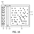
図1A及び図1Bは、本発明の実施の形態での使用のための、面内電気泳動画素の例の断面図CRS及び平面図PLNをそれぞれ示す。画素15は、第一の駆動電極10、第二の駆動電極12及びビューイング電極14を有する。画素15は、第一の駆動電極及び第二の駆動電極並びにビューイング電極に印加される制御信号の影響下で移動する帯電された黒の粒子16を更に有する。これらの制御信号は、様々な電極の周辺(すなわち様々な電極の領域、様々な電極の直接的に上又は下のエリア、或いは様々な電極に直接に隣接するエリア)間で帯電された黒の粒子16を移動する。画素は、概念的(すなわち仮想的、非現実的又は理論的)な境界114により分割される第一の領域110及び第二の領域112を有し、この境界は、第二の駆動電極12に横たわる。
1A and 1B show a cross-sectional view CRS and a plan view PLN, respectively, of an example of an in-plane electrophoretic pixel for use in an embodiment of the present invention. The
画素15の光学的な外観は、ビューイング電極14の周辺にある粒子16の数及び分布を制御することで制御される。画素15は、反射型の画素であり、表示効果を与えるために見る人122に対して光120を反射するビューイング電極14の下にある反射レイヤ118を有する。反射レイヤ118は、ビューイング電極14と少なくとも同じエリアにわたり典型的に延びる。ビューイング電極14の周辺にある粒子が多くなると、見る人に対して少ない光120が反射され、画素が暗く見える。反射レイヤ118は、明確さのために平面図で示されていない。代替的に、ビューイング電極14は反射型であり、これにより反射レイヤ118の必要が除かれる。
The optical appearance of the
画素15の粒子116は正に帯電され、印加された電場と同じ方向で、すなわち最も低い電位を有する電極に向かって移動する。しかし、他のディスプレイの画素において、粒子116は、負に帯電され、したがって当業者にとって明らかであるように、印加された電場に対して反対の方向で移動する。
The
境界114は、第二の領域112から第一の領域110を分離する。第二の駆動電極12が第一の駆動電極10とビューイング電極14の両者よりも高い電位であるとき、(第一の領域110内の)境界14の左への位置を有する正に帯電された粒子116は、第一の駆動電極10に向けて引き付けられ、(第二の領域112内の)境界114の右への位置を有する正に帯電された粒子116は、ビューイング電極14に向けて引き付けられる。
A
本発明の実施の形態は、図2A〜図2Eを参照して以下に記載される。これらの図は、(図2Aで示される)リセット段階RST、(図2Bで示される)プレアドレス指定の段階PRA、(図2Cで示される)アドレス指定の段階ADD、(図2Dで示される)ポストアドレス指定の段階POA、及び(図2Eに示される)進化の段階EVLの終わりでの、図1の電気泳動画素15内での粒子の分布を示す。粒子116は、実線の黒のエリアとして集合的に示されている。
Embodiments of the present invention are described below with reference to FIGS. 2A-2E. These figures show a reset stage RST (shown in FIG. 2A), a pre-addressing stage PRA (shown in FIG. 2B), an addressing stage ADD (shown in FIG. 2C), (shown in FIG. 2D). FIG. 2 shows the distribution of particles in the
はじめに、リセット段階RSTの間、全ての粒子116を第一の駆動電極10の周辺に移動するため、制御信号は、画素15の電極に印加される。粒子116は正に帯電されているので、第二の駆動電極12よりも低い電位を第一の駆動電極10が有し、ビューイング電極14よりも低い電位を第二の駆動電極12が有するために制御信号を印加することで、粒子は第一の駆動電極10に向けて引き付けられる。代替的に、第二の駆動電極及びビューイング電極は、同じ電位に設定され、第一の駆動電極は、より低い電位に設定される。
First, during the reset phase RST, a control signal is applied to the electrode of the
図2Aは、リセット段階RSTの終わりでの、第一の駆動電極10の周辺での(すなわち第一の駆動電極に直接隣接する)全ての帯電粒子116を示す。
FIG. 2A shows all charged
リセットステージRSTの直後には、ポストアドレス指定の段階PRAが続く。プレアドレス指定の段階PRAの間、全ての粒子116は、第二の駆動電極12の周辺に到達するまで、第二の駆動電極12に向けて移動される。粒子116は正に帯電されているので、第一の駆動電極10よりも低い電位を第二の駆動電極12が有するために制御信号を印加することで、第二の駆動電極12に移動される。制御信号は、第二の駆動電極12の周辺に粒子が到達するために十分に長い間、第一及び第二の駆動電極に印加され、これにより、ビューイング電極14の電位は、第二の駆動電極の電位よりも高くなるか又は低くなる。代替的に、制御信号は、第二の駆動電極に粒子が到達するために必要な時間よりも長い間、第一の及び第二の駆動電極に印加され、この場合、第二の駆動電極は、プレアドレス指定の段階の間にビューイング電極の周辺に粒子が移動するのを防止するため、ビューイング電極よりも低い電位を有する。
Immediately after the reset stage RST, a post addressing stage PRA follows. During the pre-addressing phase PRA, all
図2Bは、プレアドレス指定の段階PRAの終わりで、第二の駆動電極12の周辺における全ての帯電された粒子を示す。
FIG. 2B shows all charged particles around the
プレアドレス指定の段階PRAの直後には、アドレス指定の段階ADDが続く。アドレス指定の段階ADDの間、粒子16は、所望の光学状態に依存して、境界114の一方のサイド及び他方のサイド、すなわち第一の領域110及び第二の領域112に移動される。それぞれの粒子116が境界114の一方のサイド又は他方のサイドに移動しなければならない距離は短く、したがってアドレス指定の段階のために必要とされる時間は、これに応じて短い。
Immediately after the pre-addressing stage PRA, an addressing stage ADD follows. During the addressing phase ADD, the
第一の駆動電極10及び第二の駆動電極12よりも低い電位をビューイング電極14が有するために画素15に制御信号を印加することで、粒子は第二の領域112に移動され、これにより、ビューイング電極14に向けて粒子116が引き付けられる。第一の駆動電極10及び第二の駆動電極12よりも高い電位をビューイング電極14が有するために制御信号を印加することで、粒子は第一の領域110に移動され、これにより、ビューイング電極14から粒子116が離れる。
By applying a control signal to the
図2Cは、段階ADDの終わりで、粒子116がビューイング電極14に向けて(短い距離だけ)引き付けられ、粒子116の3分の1が第一の領域110にあり、粒子116の3分の2が第二の領域112にあることを示す。
FIG. 2C shows that at the end of stage ADD,
アドレス指定の段階ADDの直後には、ポストアドレス指定の段階POAが続く。ポストアドレス指定の段階POAの間、第一の領域110における粒子116は、第一の駆動電極10の周辺に移動され、第二の領域112における粒子は、ビューイング電極14の周辺に移動される。
Immediately following the addressing stage ADD is a post-addressing stage POA. During the post-addressing phase POA, the
第一の駆動電極10とビューイング電極14の両者よりも高い電位を第二の駆動電極12が有するために制御信号を画素の電極に印加することで、粒子は移動され、これにより、第一の領域110における粒子は第一の駆動電極に向かい、第二の領域112における粒子はビューイング電極に向かう。
Since the
図2Dは、ポストアドレス指定の段階POAの終わりで、粒子116の3分の1が第一の駆動電極10の周辺(このケースでは第一の駆動電極10の真上)に移動され(跳ね返され)、粒子116の3分の2がビューイング電極14の周辺(このケースでは真上)に移動される(跳ね返される)点を示す。
FIG. 2D shows that at the end of the post-addressing phase POA, one third of the
ポストアドレス指定の段階POAの直後には、進化の段階EVLが続く。進化の段階EVLの間、ビューイング電極14の周辺に移動される粒子116は、ビューイング電極14にわたり実質的に一様に分布される。これは、ある期間を通して、ビューイング電極14にわたり粒子が拡散する(ランダムに移動する)のを可能にすることで達成されるか、粒子が一様に分布されるように、ビューイング電極にわたり粒子を「シェイク」するように、ビューイング電極と第二の駆動電極との間で交流の電場を印加することで達成される。
Immediately after the post-addressing stage POA, an evolution stage EVL follows. During the evolution stage EVL, the
図2Eは、進化の段階EVLの終わりで、帯電粒子116の3分の1が第一の駆動電極にわたり一様に分布し、帯電粒子116の3分の2がビューイング電極にわたり一様に分布する点を示す。
FIG. 2E shows that at the end of the evolutionary stage EVL, one third of the charged
任意に、それぞれの画素は、第二の領域において(たとえばビューイング電極と第二の駆動電極との間)ビューイング電極に隣接して位置される更なる電極を更に有する。更なる電極は、進化の段階の間にビューイング電極にわたり粒子の分布を容易にするため、制御信号で駆動される。 Optionally, each pixel further comprises an additional electrode positioned adjacent to the viewing electrode in the second region (eg, between the viewing electrode and the second drive electrode). The further electrode is driven with a control signal to facilitate the distribution of the particles across the viewing electrode during the stage of evolution.
リセット段階RSTは、全ての粒子の位置がプレアドレス指定の段階が開始する前に既知であるように、第一の駆動電極10に全ての粒子を収集するために使用される。次いで、プレアドレス指定の段階の終わりに、第一の駆動電極10の周辺内で開始されるために全ての粒子が既知であるので、粒子116の位置は、より正確に予測される。プレアドレス指定の段階の終わりで粒子の位置を正確に予測できることは、アドレス指定の段階の間に、境界114のどのサイドに粒子116が移動されるかに関して更に正確な制御を可能にする。
The reset phase RST is used to collect all particles on the
代替的なプレアドレス指定の段階において、粒子116は、第二の駆動電極12に向けて第一の駆動電極10の周辺から移動されるが、第二の駆動電極12の周辺に完全に粒子116を移動するほどではない。したがって、プレアドレス指定の段階の終わりで、粒子116は、第一の領域110にある。これは、粒子116の何れもが境界114を横断して第二の領域112に入らないという利点を有する。したがって、粒子116がアドレス指定の段階の間に第二の領域112に意図的にではなく移動し、画素15の所望の光学的な外観においてエラーを与える可能性がない。
In an alternative pre-addressing stage, the
変更された駆動方法では、リセット段階が実現されず、したがってプレアドレス指定の段階の間、粒子116は、第一の駆動電極10及びビューイング電極14の両者から第二の駆動電極に向けて引き付けられる。これは、画素がプレアドレス指定の段階を開始するまで、画素の以前の光学的な外観が不変のままであるという利点を有する。さらに、粒子は、(たとえばリセット段階について)ビューイング電極の周辺から第一の駆動電極の周辺に移動するために進行し、次いで第二の駆動電極の周辺に戻るとき、ビューイング電極の周辺から第二の駆動電極の周辺まで移動するように進行する必要がない。したがって、画素の光学的な外観を設定するために必要とされる時間を低減することができる。
In the modified drive method, the reset phase is not realized, so that during the pre-addressing phase, the
図3は、電気泳動ディスプレイの概念図を示す。典型的な電気泳動ディスプレイは、簡単のために、図3のディスプレイは図1の画素15の3行及び2列のアレイ30及び電子駆動回路35を有するが、数百の画素を含む。画素は、PIX1、PIX2、PIX3、PIX4、PIX5及びPIX6としてラベル付けされる。画素は、画素を分割する壁32により間隔を隔てて配置される第一の基板と第二の基板(明確さのために図示せず)の間に形成される。それぞれの画素は、第一の駆動電極10、第二の駆動電極12及びビューイング電極14を有する。明確さため、PIX1及びPIX6の電極のみが図でラベル付けされる。
FIG. 3 shows a conceptual diagram of an electrophoretic display. A typical electrophoretic display includes, for simplicity, the display of FIG. 3 has a three-row and two-
コモン電極CFEは、共通の制御信号をアレイの画素の全ての第一の駆動電極10に供給する。画素のそれぞれの行は、行の画素の第二の駆動電極12に制御信号を供給するそれぞれの行の電極(R1,R2,R3)と関連付けされ、画素のそれぞれの列は、列の画素のビューイング電極14に制御信号を供給するそれぞれの列電極(C1,C2)と関連付けされる。第二の駆動電極12は、行電極R1,R2及びR3の部分により効果的に形成される。
The common electrode CFE supplies a common control signal to all the
列電極C1及びC2、コモン電極CFE、第一の駆動電極10及びビューイング電極14は、第一の基板上に全て形成される。行電極R1,R2及びR3、並びに第二の駆動電極12は、画素を分割する壁32及び電気泳動媒体により第一の基板から間隔を隔てて配置される第二の基板上に全て形成される。
The column electrodes C1 and C2, the common electrode CFE, the
代替的に、行電極R1、R2及びR3、並びに第二の駆動電極12は、クロスオーバ絶縁層により他の電極から電気的に分離されている第一の基板上に形成される。
Alternatively, the row electrodes R1, R2 and R3 and the
駆動回路35は、R1、R2、R3、C1及びC2、並びにCFE電極を駆動するために制御信号を供給する。駆動回路は、電圧レンジが使用されるディスプレイの画素の電圧要件に従って明らかに変動するが、−10〜+10ボルトの範囲に及ぶ制御信号を供給する。
The
本実施の形態の駆動回路35は、第一の基板又は第二の基板上に集積され、薄膜トランジスタ(TFT)を有する。代替的に、駆動回路は、フィールドプログラマブルゲートアレイ(FPGA)、特定用途向け集積回路(ASIC)、又は指定されたやり方で画素アレイを駆動するために制御信号を発生するために構成される他の回路である。
The
画素PIX1−PIX6の光学的な外観を設定するために駆動回路35により電極R1,R2,R3,C1,C2及びCFEに印加される制御信号は、図4に示されるタイミング図を参照して以下に記載される。
The control signals applied to the electrodes R1, R2, R3, C1, C2 and CFE by the
図4のタイミング図は、R1,R2,R3,C1、C2及びCFE電極に印加される電圧及び画素のそれぞれの行の段階(PIX1及びPIX2,PIX3及びPIX4、PIX5及びPIX6)を示すトレースを有する。 The timing diagram of FIG. 4 has traces showing the voltages applied to the R1, R2, R3, C1, C2 and CFE electrodes and the respective row stages of the pixels (PIX1 and PIX2, PIX3 and PIX4, PIX5 and PIX6). .
行電極は、異なる段階を通して画素のそれぞれの行をステップするために使用され、列電極は、画素の所望の光学的な外観を設定するため、データを供給するために使用される。タイミング図では、電圧レベルDPIX1、DPIX2、DPIX3、DPIX4、DPIX5及びDPIX6は、画素PIX1、PIX2、PIX3、PIX4、PIX5及びPIX6の光学的な外観をそれぞれ設定するために使用される。 Row electrodes are used to step each row of pixels through different stages, and column electrodes are used to supply data to set the desired optical appearance of the pixels. In the timing diagram, voltage levels DPIX1, DPIX2, DPIX3, DPIX4, DPIX5 and DPIX6 are used to set the optical appearance of pixels PIX1, PIX2, PIX3, PIX4, PIX5 and PIX6, respectively.
最後に、全ての画素PIX1−PIX6は、コモン電極CFEを0Vに、行電極R1,R2及びR3を+5Vに、及び列電極C1及びC2を+10Vに設定することで、リセット段階RSTで設定される。したがって、それぞれの画素の正に帯電された粒子116は、画素の第一の駆動電極10の周辺に移動する。ひとたび、粒子116が第一の駆動電極10の周辺に移動されると、行電極R1、R2及びR3は+10に設定され、列電極C1及びC2は0Vに設定され、これにより、それぞれの画素の粒子116をそれぞれの画素の第一の駆動電極10の周辺に保持する。
Finally, all the pixels PIX1-PIX6 are set in the reset stage RST by setting the common electrode CFE to 0V, the row electrodes R1, R2 and R3 to + 5V and the column electrodes C1 and C2 to + 10V. . Accordingly, the positively charged
つぎに、画素PIX1及びPIX2の第一の行は、行電極R1を−5Vに設定することでプレアドレス指定の段階PRAにおいて設定される。したがって、画素PIX1及びPIX2の粒子116は、画素PIX1及びPIX2のそれぞれの第二の駆動電極12に向かって移動する。プレアドレス指定の段階は、粒子116がPIX1及びPIX2の第二の駆動電極12の周辺に移動するために十分に長く続く。
Next, the first row of pixels PIX1 and PIX2 is set in the pre-addressing stage PRA by setting the row electrode R1 to -5V. Therefore, the
つぎに、画素PIX3及びPIX4の第二の行は、プレアドレス指定の段階PRAで設定され、画素の第一の行は、アドレス指定の段階ADDで設定される。 Next, the second row of pixels PIX3 and PIX4 is set in the pre-addressing stage PRA, and the first row of pixels is set in the addressing stage ADD.
画素PIX3及びPIX4の第二の行は、行電極R2を−5Vに設定することでプレアドレス指定の段階PRAで設定される。したがって、画素PIX3及びPIX4の粒子116は、画素PIX3及びPIX4のそれぞれの第二の駆動電極12に向かって移動する。
The second row of pixels PIX3 and PIX4 is set at the pre-addressing stage PRA by setting the row electrode R2 to -5V. Accordingly, the
画素の第一の行は、行電極R1を0Vに設定し、列C1及びC2を電圧レベルDPIX1及びDPIX2のそれぞれに設定することで、アドレス指定の段階ADDで設定される。電圧レベルDPIX1及びDPIX2は、画素PIX1及びPIX2の所望の光学的な外観のそれぞれに依存する。たとえば、PIX1の粒子116が第一の領域に移動される場合、電圧レベルDPIX1は、粒子116がビューイング電極14から離れるために+5Vである。PIX1の粒子116が第二の領域に移動される場合、電圧レベルDPIX1は、ビューイング電極14に向かって粒子116を引き付けるために−5Vである。
The first row of pixels is set at the addressing stage ADD by setting the row electrode R1 to 0V and the columns C1 and C2 to voltage levels DPIX1 and DPIX2, respectively. The voltage levels DPIX1 and DPIX2 depend on the desired optical appearance of the pixels PIX1 and PIX2, respectively. For example, if the
つぎに、画素PIX5及びPIX6の第三の行は、プレアドレス指定の段階PRAで設定され、画素PIX3及びPIX4の第二の行は、アドレス指定の段階ADDで設定され、画素PIX1及びPIX2の第一の行は、ポストアドレス指定の段階POAにおいて設定される。 Next, the third row of pixels PIX5 and PIX6 is set in the pre-addressing stage PRA, and the second row of pixels PIX3 and PIX4 is set in the addressing stage ADD, and the second row of pixels PIX1 and PIX2 One row is set in the post addressing phase POA.
画素PIX5及びPIX6の第三の行は、行電極R3を−5Vに設定することでプレアドレス指定の段階PRAで設定される。したがって、画素PIX5及びPIX6の粒子116は、画素PIX5及びPIX6の第二の駆動電極12に向かってそれぞれ移動する。
The third row of pixels PIX5 and PIX6 is set at the pre-addressing stage PRA by setting the row electrode R3 to -5V. Accordingly, the
画素の第二の行は、行電極R2を0Vに設定し、列電極C1及びC2を電圧レベルDPIX3及びDPIX4のそれぞれに設定することでアドレス指定の段階ADDで設定される。電圧レベルDPIX3及びDPIX4は、画素PIX3及びPIX4の所望の光学的な外観にそれぞれ依存する。たとえば、PIX3の粒子116が第一の領域に移動される場合、電圧レベルDPIX3は、粒子116がビューイング電極14から離れるために+5Vである。PIX3の粒子116が第二の領域に移動される場合、電圧レベルDPIX3は、粒子116がビューイング電極14に向かって引き付けられるために−5Vである。
The second row of pixels is set at the addressing stage ADD by setting the row electrode R2 to 0V and the column electrodes C1 and C2 to voltage levels DPIX3 and DPIX4, respectively. The voltage levels DPIX3 and DPIX4 depend on the desired optical appearance of the pixels PIX3 and PIX4, respectively. For example, if the
画素の第一の行は、行電極R1を+10Vに設定することで、ポストアドレス指定の段階POAで設定される。したがって、画素PIX1及びPIX2の粒子116は、アドレス指定の段階ADDの後、粒子116が第一の領域110又は第二の領域112にあったかに依存して、第一の駆動電極10又はビューイング電極14に向かって移動する。たとえば、アドレス指定の段階ADDの後にPIX1の粒子116が第一の領域110にあった場合、行電極R1を+10Vに設定することで、粒子116は、第一の駆動電極10の周辺に移動する。
The first row of pixels is set at the post addressing stage POA by setting the row electrode R1 to + 10V. Thus, the
つぎに、画素PIX5及びPIX6の第三の行は、アドレス指定の段階ADDで設定され、画素PIX3及びPIX4の第二の行は、ポストアドレス指定の段階POAで設定される。 Next, the third row of pixels PIX5 and PIX6 is set in the addressing stage ADD, and the second row of pixels PIX3 and PIX4 is set in the post-addressing stage POA.
画素の第三の行は、行電極R3を0Vに設定し、列電極C1及びC2を電圧レベルDPIX5及びDPIX6のそれぞれに設定することで、アドレス指定の段階ADDで設定される。電圧レベルDPIX5及びDPIX6は、画素PIX5及びPIX6のそれぞれの所望の光学的な外観に依存する。たとえば、画素PIX5の粒子116が第一の領域に移動される場合、電圧レベルDPIX5は、粒子116がビューイング電極14から離れるために+5Vである。画素PIX5の粒子116が第二の領域に移動される場合、電圧レベルDPIX5は、粒子116がビューイング電極14に向かって引き付けられるために−5Vである。
The third row of pixels is set at the addressing stage ADD by setting the row electrode R3 to 0V and the column electrodes C1 and C2 to voltage levels DPIX5 and DPIX6, respectively. The voltage levels DPIX5 and DPIX6 depend on the desired optical appearance of the pixels PIX5 and PIX6, respectively. For example, if the
画素の第二の行は、行電極R2を+10Vに設定することでポストアドレス指定の段階POAで設定される。したがって、アドレス指定の段階ADDの後に粒子116が第一の領域110にあったか又は第二の領域112にあったかに依存して、画素PIX3及びPIX4の粒子116は、第一の駆動電極10又はビューイング電極14に向かって移動する。たとえば、PIX3の粒子116がアドレス指定の段階ADDの後に第一の領域110にあった場合、行電極R2を+10Vに設定することで、粒子116は、第一の駆動電極10の周辺に移動する。
The second row of pixels is set at the post addressing stage POA by setting the row electrode R2 to + 10V. Thus, depending on whether the
つぎに、画素PIX5及びPIX6の第三の行は、行電極R3を+10Vに設定することで、ポストアドレス指定の段階POAで設定される。したがって、アドレス指定の段階ADDの後に粒子116が第一の領域110にあったか又は第二の領域112にあったかに依存して、画素PIX5及びPIX6の粒子116は、第一の駆動電極10又はビューイング電極14に向かって移動する。たとえば、PIX5の粒子116がアドレス指定の段階ADDの後に第一の領域110にあった場合、行電極R3を+10Vに設定することで、粒子116は、第一の駆動電極10の周辺に移動する。
Next, the third row of pixels PIX5 and PIX6 is set at the post addressing stage POA by setting the row electrode R3 to + 10V. Thus, depending on whether the
最後に、画素は、進化の段階EVLで設定され、ここで、ポストアドレス指定の段階の間にビューイング電極の周辺に移動されている粒子には、ビューイング電極にわたり一様に分散する時間が与えられる。任意に、画素は、進化の段階を容易にする更なる電極を有する。 Finally, the pixels are set in the evolution stage EVL, where particles that have been moved to the periphery of the viewing electrode during the post-addressing stage have a time that is evenly distributed across the viewing electrode. Given. Optionally, the pixel has additional electrodes that facilitate the stage of evolution.
図4で見ることができるように、駆動方法は、アドレス指定の段階ADDにおいて画素の第二の行を設定する段階を含み、画素の第一の行は、ポストアドレス指定の段階POAで設定され、画素の第三の行は、プレアドレス指定の段階PRAで設定される。したがって、プレアドレス指定及びポストアドレス指定の段階は、これらが他の画素がアドレス指定されている間に行なわれるので、アレイ内の全ての画素について光学的な外観を設定するために必要とされる全体の時間を著しく追加しない。 As can be seen in FIG. 4, the driving method includes setting a second row of pixels in the addressing stage ADD, the first row of pixels being set in the post-addressing stage POA. The third row of pixels is set at the pre-addressing stage PRA. Thus, the pre-addressing and post-addressing steps are required to set the optical appearance for all the pixels in the array since they are performed while other pixels are being addressed. Does not add significant overall time.
代替的に、プレアドレス指定又はポストアドレス指定の段階は、アドレス指定の段階よりも長い期間について続き、ある行は、2以上のアドレス指定の段階の期間についてプレアドレス指定又はポストアドレス指定の段階で設定される。したがって、2以上の行は、プレアドレス指定の段階にあり、及び/又は2以上の行は、時間的に同じ瞬間で、ポストアドレス指定の段階にある。たとえば、画素の第一の行はアドレス指定の段階にあり、画素の第二及び第三の行はプレアドレス指定の段階にある。 Alternatively, the pre-addressing or post-addressing phase lasts for a longer period of time than the addressing phase, and a row is in the pre-addressing or post-addressing phase for two or more addressing phase periods. Is set. Thus, two or more rows are in the pre-addressing phase and / or two or more rows are in the post-addressing phase at the same instant in time. For example, the first row of pixels is in the addressing stage and the second and third rows of pixels are in the pre-addressing stage.
異なる段階のために必要とされる正確な時間の長さは、画素に印加される駆動信号の電圧(すなわち電場の強度)を変更することで変更される。これは、高い電場の強度によって、粒子はより迅速に移動し、したがって当業者にとって明らかであるように、必要とされる距離を粒子が移動するために必要とされる時間が低減されるためである。 The exact amount of time required for the different stages is changed by changing the voltage of the drive signal applied to the pixel (ie, the strength of the electric field). This is because the high electric field strength causes the particles to move more quickly, thus reducing the time required for the particles to travel the required distance, as will be apparent to those skilled in the art. is there.
プレアドレス指定の段階の間に行電極に印加される電圧は、−5V〜−4Vに増加され、画素の第一の駆動電極と第二の駆動電極の間の電場強度が低減され、したがって、プレアドレス指定の段階のために許容される時間の間に第二の電極に向かって粒子が進行する距離が低減される。したがって、粒子は、第二の駆動電極の周辺に移動しない場合がある。左記に説明されたように、これは、粒子が画素の第二の領域に意図的にではなく移動し、画素の所望の光学的な外観におけるエラーを与える可能性がないという利点を有する。 The voltage applied to the row electrode during the pre-addressing phase is increased from -5V to -4V, reducing the electric field strength between the first drive electrode and the second drive electrode of the pixel, and thus The distance traveled by the particles towards the second electrode during the time allowed for the pre-addressing phase is reduced. Therefore, the particles may not move around the second drive electrode. As explained on the left, this has the advantage that the particles move unintentionally into the second region of the pixel and can not give an error in the desired optical appearance of the pixel.
概説すると、表示装置及び該表示装置を駆動する方法が開示された。この表示装置は、駆動回路及び移動可能な帯電粒子を含む複数の画素を有する。駆動回路は、それぞれの画素の光学的な外観を変更するため、それぞれの画素の第一の領域と第二の領域の間で帯電された粒子を移動するために画素に制御信号を印加するために構成される。それぞれの画素の方法は、第一の領域と第二の領域との間の境界に向かって帯電された粒子を移動するプレアドレス指定の段階、次いで、画素の所望の光学的な外観に依存して、境界の一方のサイド又は他のサイドに粒子を移動するアドレス指定の段階を含む。 In general, a display device and a method for driving the display device have been disclosed. This display device includes a plurality of pixels including a driving circuit and movable charged particles. The drive circuit applies a control signal to the pixel to move the charged particles between the first and second regions of each pixel in order to change the optical appearance of each pixel Configured. Each pixel method depends on a pre-addressing stage that moves the charged particles towards the boundary between the first and second regions, and then the desired optical appearance of the pixel. And an addressing step of moving the particles to one side or the other side of the boundary.
特許請求の範囲に含まれる様々な他の実施の形態は、当業者にとって明らかである。たとえば、特許請求の範囲で述べたやり方で画素の第一の領域と第二の領域との間で粒子を移動させるため、様々な電極が設定される多数の異なる電位が存在する。特に、移動可能な帯電された粒子は、正に帯電される代わりに負に帯電され、実施の形態で説明された駆動信号の極性が類似の粒子の移動を得るために反転されることが必要とされる。請求項における参照符号は、請求の範囲を制限するように解釈されるべきではない。
Various other embodiments within the scope of the claims will be apparent to those skilled in the art. For example, there are a number of different potentials at which the various electrodes are set to move the particles between the first and second regions of the pixel in the manner described in the claims. In particular, movable charged particles must be negatively charged instead of positively charged, and the polarity of the drive signal described in the embodiment must be reversed to obtain similar particle movement. It is said. Any reference signs in the claims should not be construed as limiting the scope.
Claims (10)
それぞれの画素は、
画素の第一の領域に関連される第一の駆動電極と、
画素の第二の領域に関連されるビューイング電極と、
画素の前記第一の領域と前記第二の領域との間の境界であって、前記第一の駆動電極と前記ビューイング電極の中間にある第二の駆動電極と、
移動可能な帯電粒子とを有し、
それぞれの画素の光学的な外観は、前記第一及び第二の駆動電極及び前記ビューイング電極に印加される制御信号の影響下で、前記ビューイング電極の周辺での帯電粒子の数を制御することで変更され、
当該方法は、それぞれの画素について、
プレアドレス指定の段階で、制御信号を画素に印加して、前記第一の領域と前記第二の領域の間の境界で前記第二の駆動電極に向けて粒子を移動させるステップと、
アドレス指定の段階で、制御信号を画素に印加して、画素の所望の光学的な外観に依存して、前記第一の領域及び前記第二の領域に粒子を移動させるステップとを含み、
当該方法は、
前記アドレス指定の段階に続くポストアドレス指定の段階であって、前記第一の領域における粒子が前記第一の駆動電極の周辺に移動し、前記第二の領域における粒子が前記ビューイング電極の周辺に移動するように、前記画素に制御信号を印加することを含むポストアドレス指定の段階と、
前記ポストアドレス指定の段階に続く進化の段階であって、制御信号を全ての画素に印加して、前記ビューイング電極にわたり前記ビューイング電極の周辺におけるそれぞれの画素の粒子を分散させることを含む進化の段階と、
を更に含むことを特徴とする駆動方法。 A driving method of an in-plane electrophoretic display device having a plurality of pixels arranged in an array of rows and columns,
Each pixel is
A first drive electrode associated with the first region of the pixel;
A viewing electrode associated with the second region of the pixel;
A second drive electrode that is a boundary between the first region and the second region of a pixel and is intermediate the first drive electrode and the viewing electrode;
Movable charged particles,
The optical appearance of each pixel controls the number of charged particles around the viewing electrode under the influence of control signals applied to the first and second drive electrodes and the viewing electrode. Changed
For each pixel, the method
At a pre-addressing stage, applying a control signal to the pixel to move the particles towards the second drive electrode at the boundary between the first region and the second region;
Applying a control signal to the pixel at the addressing stage to move particles to the first region and the second region depending on the desired optical appearance of the pixel;
The method is
A post-addressing stage following the addressing stage, wherein particles in the first region move around the first drive electrode and particles in the second region move around the viewing electrode Post-addressing comprising applying a control signal to the pixel to move to
An evolutionary step following the post-addressing step, comprising applying a control signal to all pixels to disperse particles of each pixel around the viewing electrode across the viewing electrode And the stage
The driving method further comprising:
請求項1記載の駆動方法。 The pre-addressing stage includes moving the particles toward the second drive electrode until the particles reach the periphery of the second drive electrode;
The driving method according to claim 1.
請求項1又は2記載の駆動方法。 The pre-addressing step includes a step in which particles do not move completely around the second drive electrode, but particles move toward the second drive electrode;
The driving method according to claim 1 or 2.
請求項1乃至3の何れか記載の駆動方法。 When at least one of a plurality of pixels is in the pre-addressing stage, another pixel of the plurality of pixels is in the addressing stage;
The driving method according to claim 1.
請求項1記載の駆動方法。 When at least one of the plurality of pixels is in the post-addressing stage, at least one other pixel of the plurality of pixels is in the addressing stage;
The driving method according to claim 1.
前記リセットステージは、制御信号を全ての画素に印加して、それぞれの画素の前記第一の駆動電極の周辺にそれぞれの画素の粒子を移動する、
請求項1乃至5の何れか記載の駆動方法。 A reset stage preceding the pre-addressing stage;
The reset stage applies a control signal to all pixels to move the particles of each pixel around the first drive electrode of each pixel.
The driving method according to claim 1.
それぞれの行電極は、それぞれの行に含まれる画素の制御信号を供給し、
それぞれの列電極は、それぞれの列に含まれる画素に制御信号を供給する、
請求項1乃至6の何れか記載の駆動方法。 The plurality of pixels includes a row and column array, and the array includes a row electrode and a column electrode,
Each row electrode supplies a control signal for the pixels included in each row,
Each column electrode supplies a control signal to the pixels included in each column.
The driving method according to claim 1.
請求項7記載の駆動方法。 A row of pixels is all in the pre-addressing stage while all adjacent pixel rows are in the addressing stage.
The driving method according to claim 7.
当該駆動方法は、
前記第一、第二及び第三の画素の行を前記リセットの段階に設定し、
前記第一の画素の行を前記プレアドレス指定の段階に設定し、次いで、前記第二の画素の行を前記プレアドレス指定の段階に設定し、次いで、第三の画素の行を前記プレアドレス指定の段階に設定し、
前記第一の画素の行を前記アドレス指定の段階に設定し、次いで、前記第二の画素の行を前記アドレス指定の段階に設定し、次いで、第三の画素の行を前記アドレス指定の段階に設定し、
前記第一の画素の行を前記ポストアドレス指定の段階に設定し、次いで、前記第二の画素の行を前記ポストアドレス指定の段階に設定し、次いで、第三の画素の行を前記ポストアドレス指定の段階に設定し、
前記第一、第二及び第三の画素の行を前記進化の段階に設定するステップと、
を含む請求項7又は8記載の駆動方法。 The array has at least a first row of pixels, a second row of pixels, and a third row of pixels;
The driving method is
Setting the first, second and third pixel rows to the reset stage;
The first row of pixels is set to the pre-addressing stage, then the second row of pixels is set to the pre-addressing stage, and then the third row of pixels is set to the pre-addressing stage. Set to the specified stage,
Setting the first pixel row to the addressing stage, then setting the second pixel row to the addressing stage, and then setting the third pixel row to the addressing stage. Set to
The first pixel row is set to the post-addressing stage, then the second pixel row is set to the post-addressing stage, and then a third pixel row is set to the post-addressing stage. Set to the specified stage,
Setting the first, second and third pixel rows to the stage of evolution;
The drive method of Claim 7 or 8 containing these.
それぞれの画素は、
画素の第一の領域に関連される第一の駆動電極と、
画素の第二の領域に関連されるビューイング電極と、
画素の前記第一の領域と前記第二の領域との間の境界であって、前記第一の駆動電極と前記ビューイング電極の中間にある第二の駆動電極と、
移動可能な帯電粒子とを有し、
それぞれの画素の光学的な外観は、前記第一及び第二の駆動電極及び前記ビューイング電極に印加される制御信号の影響下で、前記ビューイング電極の周辺での帯電粒子の数を制御することで変更され、
当該表示装置は、電子駆動回路を更に有し、
前記駆動回路は、それぞれの画素について、
プレアドレス指定の段階で、制御信号を画素に印加して、前記第一の領域と前記第二の領域の間の境界で前記第二の駆動電極に向けて粒子を移動し、
アドレス指定の段階で、制御信号を画素に印加して、画素の所望の光学的な外観に依存して、前記第一の領域及び前記第二の領域に粒子を移動し、
前記アドレス指定の段階に続くポストアドレス指定の段階であって、前記第一の領域における粒子が前記第一の駆動電極の周辺に移動し、前記第二の領域における粒子が前記ビューイング電極の周辺に移動するように、前記画素に制御信号を印加し、
前記ポストアドレス指定の段階に続く進化の段階であって、制御信号を全ての画素に印加して、前記ビューイング電極にわたり前記ビューイング電極の周辺におけるそれぞれの画素の粒子を分散させる、
ことを特徴とする駆動方法。 An in-plane electrophoretic display device having a plurality of pixels arranged in an array of rows and columns,
Each pixel is
A first drive electrode associated with the first region of the pixel;
A viewing electrode associated with the second region of the pixel;
A second drive electrode that is a boundary between the first region and the second region of a pixel and is intermediate the first drive electrode and the viewing electrode;
Movable charged particles,
The optical appearance of each pixel controls the number of charged particles around the viewing electrode under the influence of control signals applied to the first and second drive electrodes and the viewing electrode. Changed
The display device further includes an electronic drive circuit,
The drive circuit for each pixel
At the pre-addressing stage, a control signal is applied to the pixel to move the particles toward the second drive electrode at the boundary between the first region and the second region,
At the addressing stage, a control signal is applied to the pixel to move particles to the first region and the second region, depending on the desired optical appearance of the pixel,
A post-addressing stage following the addressing stage, wherein particles in the first region move around the first drive electrode and particles in the second region move around the viewing electrode A control signal is applied to the pixel so as to move to
An evolutionary step following the post-addressing step, wherein a control signal is applied to all pixels to disperse particles of each pixel around the viewing electrode across the viewing electrode;
A driving method characterized by that.
Applications Claiming Priority (3)
| Application Number | Priority Date | Filing Date | Title |
|---|---|---|---|
| EP06118965 | 2006-08-15 | ||
| EP06118965.0 | 2006-08-15 | ||
| PCT/IB2007/053005 WO2008020355A2 (en) | 2006-08-15 | 2007-07-30 | Moving particle display device |
Publications (2)
| Publication Number | Publication Date |
|---|---|
| JP2010500624A JP2010500624A (en) | 2010-01-07 |
| JP5554059B2 true JP5554059B2 (en) | 2014-07-23 |
Family
ID=38962008
Family Applications (1)
| Application Number | Title | Priority Date | Filing Date |
|---|---|---|---|
| JP2009524263A Expired - Fee Related JP5554059B2 (en) | 2006-08-15 | 2007-07-30 | Improved display device |
Country Status (8)
| Country | Link |
|---|---|
| US (1) | US8982041B2 (en) |
| EP (1) | EP2054759B1 (en) |
| JP (1) | JP5554059B2 (en) |
| KR (1) | KR101407375B1 (en) |
| CN (1) | CN101506726B (en) |
| AT (1) | ATE535839T1 (en) |
| TW (1) | TWI454813B (en) |
| WO (1) | WO2008020355A2 (en) |
Families Citing this family (2)
| Publication number | Priority date | Publication date | Assignee | Title |
|---|---|---|---|---|
| US9201282B2 (en) | 2009-07-27 | 2015-12-01 | Hj Forever Patents B.V. | Electrophoretic display device |
| NL2010936C2 (en) | 2013-06-07 | 2014-09-25 | Hj Forever B V | Electrophoretic display. |
Family Cites Families (16)
| Publication number | Priority date | Publication date | Assignee | Title |
|---|---|---|---|---|
| US3612758A (en) | 1969-10-03 | 1971-10-12 | Xerox Corp | Color display device |
| US4203106A (en) | 1977-11-23 | 1980-05-13 | North American Philips Corporation | X-Y addressable electrophoretic display device with control electrode |
| JP3592184B2 (en) * | 2000-03-03 | 2004-11-24 | キヤノン株式会社 | Electrophoretic display device and driving method thereof |
| US6639580B1 (en) * | 1999-11-08 | 2003-10-28 | Canon Kabushiki Kaisha | Electrophoretic display device and method for addressing display device |
| JP3625421B2 (en) * | 1999-11-08 | 2005-03-02 | キヤノン株式会社 | Electrophoretic display device |
| US6822783B2 (en) * | 2001-06-26 | 2004-11-23 | Canon Kabushiki Kaisha | Electrophoretic display unit, and driving method thereof |
| TWI229763B (en) * | 2001-10-29 | 2005-03-21 | Sipix Imaging Inc | An improved electrophoretic display with holding electrodes |
| CN1668972A (en) | 2002-07-17 | 2005-09-14 | 皇家飞利浦电子股份有限公司 | In-plane switching electrophoretic display devices |
| EP1537451A1 (en) * | 2002-08-26 | 2005-06-08 | Koninklijke Philips Electronics N.V. | Electrophoretic display panel |
| US7379228B2 (en) * | 2003-01-17 | 2008-05-27 | Koninklijke Philips Electroncis N.V. | Electrophoretic display |
| JP2004271610A (en) * | 2003-03-05 | 2004-09-30 | Canon Inc | Color electrophoresis display device |
| US20050012707A1 (en) * | 2003-07-15 | 2005-01-20 | Hong-Da Liu | Electrophoretic display and a method of driving said display |
| JP4860487B2 (en) * | 2004-02-06 | 2012-01-25 | コーニンクレッカ フィリップス エレクトロニクス エヌ ヴィ | Electrophoretic display panel |
| WO2007105146A1 (en) | 2006-03-14 | 2007-09-20 | Koninklijke Philips Electronics N.V. | Driving an in-plane passive matrix display |
| EP2024959A2 (en) | 2006-05-17 | 2009-02-18 | Koninklijke Philips Electronics N.V. | Moving particle display device |
| WO2008026144A2 (en) * | 2006-08-30 | 2008-03-06 | Koninklijke Philips Electronics N.V. | In-plane switching electronphoretic display device |
-
2007
- 2007-07-30 KR KR1020097002821A patent/KR101407375B1/en active IP Right Grant
- 2007-07-30 WO PCT/IB2007/053005 patent/WO2008020355A2/en active Application Filing
- 2007-07-30 CN CN2007800304787A patent/CN101506726B/en not_active Expired - Fee Related
- 2007-07-30 JP JP2009524263A patent/JP5554059B2/en not_active Expired - Fee Related
- 2007-07-30 EP EP07825971A patent/EP2054759B1/en not_active Not-in-force
- 2007-07-30 US US12/377,606 patent/US8982041B2/en active Active
- 2007-07-30 AT AT07825971T patent/ATE535839T1/en active
- 2007-08-10 TW TW096129701A patent/TWI454813B/en not_active IP Right Cessation
Also Published As
| Publication number | Publication date |
|---|---|
| CN101506726A (en) | 2009-08-12 |
| KR20090039763A (en) | 2009-04-22 |
| WO2008020355A2 (en) | 2008-02-21 |
| JP2010500624A (en) | 2010-01-07 |
| US20100171768A1 (en) | 2010-07-08 |
| TWI454813B (en) | 2014-10-01 |
| US8982041B2 (en) | 2015-03-17 |
| CN101506726B (en) | 2013-05-08 |
| KR101407375B1 (en) | 2014-06-17 |
| ATE535839T1 (en) | 2011-12-15 |
| EP2054759A2 (en) | 2009-05-06 |
| WO2008020355A3 (en) | 2008-04-17 |
| EP2054759B1 (en) | 2011-11-30 |
| TW200816114A (en) | 2008-04-01 |
Similar Documents
| Publication | Publication Date | Title |
|---|---|---|
| JP4494963B2 (en) | Electrophoretic display and driving method of electrophoretic display | |
| KR100830106B1 (en) | Electrophoretic device and method of driving the same | |
| TWI420447B (en) | Sequential of displays | |
| JP5478255B2 (en) | Driving method and electrophoresis apparatus for electrophoresis cell | |
| KR20170110657A (en) | Electro-optic displays displaying in dark mode and light mode, and related apparatus and methods | |
| KR20070006755A (en) | Method of increasing image bi-stability and grayscale accuracy in an electrophoretic display | |
| KR20060105755A (en) | Method and apparatus for reducing edge image retention in an electrophoretic display device | |
| JP2006516749A (en) | Driving bistable matrix display devices | |
| JP5406526B2 (en) | In-plane switching display | |
| US20090160846A1 (en) | Display device | |
| US20110298838A1 (en) | Electrophoretic display | |
| JP2006525543A (en) | Electrophoretic display device | |
| JP5409352B2 (en) | Moving particle display | |
| JP5554059B2 (en) | Improved display device | |
| KR102659779B1 (en) | Methods for driving electro-optical displays | |
| JP2009530654A (en) | In-plane passive matrix display driving apparatus and method | |
| KR101991744B1 (en) | Electrophoresis display device and method for driving the same | |
| KR102659780B1 (en) | Methods for driving electro-optical displays | |
| KR20230008207A (en) | Electro-optical displays and methods for driving them | |
| JP5620863B2 (en) | Electrophoretic display device and driving method thereof |
Legal Events
| Date | Code | Title | Description |
|---|---|---|---|
| A621 | Written request for application examination |
Free format text: JAPANESE INTERMEDIATE CODE: A621 Effective date: 20100728 |
|
| A131 | Notification of reasons for refusal |
Free format text: JAPANESE INTERMEDIATE CODE: A131 Effective date: 20120612 |
|
| A601 | Written request for extension of time |
Free format text: JAPANESE INTERMEDIATE CODE: A601 Effective date: 20120910 |
|
| A602 | Written permission of extension of time |
Free format text: JAPANESE INTERMEDIATE CODE: A602 Effective date: 20120918 |
|
| A521 | Request for written amendment filed |
Free format text: JAPANESE INTERMEDIATE CODE: A523 Effective date: 20121211 |
|
| A131 | Notification of reasons for refusal |
Free format text: JAPANESE INTERMEDIATE CODE: A131 Effective date: 20130326 |
|
| A601 | Written request for extension of time |
Free format text: JAPANESE INTERMEDIATE CODE: A601 Effective date: 20130624 |
|
| A602 | Written permission of extension of time |
Free format text: JAPANESE INTERMEDIATE CODE: A602 Effective date: 20130701 |
|
| A521 | Request for written amendment filed |
Free format text: JAPANESE INTERMEDIATE CODE: A523 Effective date: 20130924 |
|
| TRDD | Decision of grant or rejection written | ||
| A01 | Written decision to grant a patent or to grant a registration (utility model) |
Free format text: JAPANESE INTERMEDIATE CODE: A01 Effective date: 20140430 |
|
| A61 | First payment of annual fees (during grant procedure) |
Free format text: JAPANESE INTERMEDIATE CODE: A61 Effective date: 20140528 |
|
| R150 | Certificate of patent or registration of utility model |
Ref document number: 5554059 Country of ref document: JP Free format text: JAPANESE INTERMEDIATE CODE: R150 |
|
| S111 | Request for change of ownership or part of ownership |
Free format text: JAPANESE INTERMEDIATE CODE: R313113 |
|
| R350 | Written notification of registration of transfer |
Free format text: JAPANESE INTERMEDIATE CODE: R350 |
|
| R250 | Receipt of annual fees |
Free format text: JAPANESE INTERMEDIATE CODE: R250 |
|
| R250 | Receipt of annual fees |
Free format text: JAPANESE INTERMEDIATE CODE: R250 |
|
| R250 | Receipt of annual fees |
Free format text: JAPANESE INTERMEDIATE CODE: R250 |
|
| S531 | Written request for registration of change of domicile |
Free format text: JAPANESE INTERMEDIATE CODE: R313531 |
|
| S533 | Written request for registration of change of name |
Free format text: JAPANESE INTERMEDIATE CODE: R313533 |
|
| R350 | Written notification of registration of transfer |
Free format text: JAPANESE INTERMEDIATE CODE: R350 |
|
| R250 | Receipt of annual fees |
Free format text: JAPANESE INTERMEDIATE CODE: R250 |
|
| R250 | Receipt of annual fees |
Free format text: JAPANESE INTERMEDIATE CODE: R250 |
|
| LAPS | Cancellation because of no payment of annual fees |