JP5551739B2 - System and method for efficient parameter correction - Google Patents
System and method for efficient parameter correction Download PDFInfo
- Publication number
- JP5551739B2 JP5551739B2 JP2012171640A JP2012171640A JP5551739B2 JP 5551739 B2 JP5551739 B2 JP 5551739B2 JP 2012171640 A JP2012171640 A JP 2012171640A JP 2012171640 A JP2012171640 A JP 2012171640A JP 5551739 B2 JP5551739 B2 JP 5551739B2
- Authority
- JP
- Japan
- Prior art keywords
- data
- circuit
- value
- data set
- parameter
- Prior art date
- Legal status (The legal status is an assumption and is not a legal conclusion. Google has not performed a legal analysis and makes no representation as to the accuracy of the status listed.)
- Expired - Fee Related
Links
Images


Classifications
-
- G—PHYSICS
- G11—INFORMATION STORAGE
- G11B—INFORMATION STORAGE BASED ON RELATIVE MOVEMENT BETWEEN RECORD CARRIER AND TRANSDUCER
- G11B27/00—Editing; Indexing; Addressing; Timing or synchronising; Monitoring; Measuring tape travel
- G11B27/36—Monitoring, i.e. supervising the progress of recording or reproducing
-
- H—ELECTRICITY
- H03—ELECTRONIC CIRCUITRY
- H03M—CODING; DECODING; CODE CONVERSION IN GENERAL
- H03M13/00—Coding, decoding or code conversion, for error detection or error correction; Coding theory basic assumptions; Coding bounds; Error probability evaluation methods; Channel models; Simulation or testing of codes
-
- G—PHYSICS
- G06—COMPUTING; CALCULATING OR COUNTING
- G06F—ELECTRIC DIGITAL DATA PROCESSING
- G06F1/00—Details not covered by groups G06F3/00 - G06F13/00 and G06F21/00
-
- G—PHYSICS
- G11—INFORMATION STORAGE
- G11B—INFORMATION STORAGE BASED ON RELATIVE MOVEMENT BETWEEN RECORD CARRIER AND TRANSDUCER
- G11B20/00—Signal processing not specific to the method of recording or reproducing; Circuits therefor
- G11B20/10—Digital recording or reproducing
- G11B20/10009—Improvement or modification of read or write signals
- G11B20/10268—Improvement or modification of read or write signals bit detection or demodulation methods
- G11B20/10287—Improvement or modification of read or write signals bit detection or demodulation methods using probabilistic methods, e.g. maximum likelihood detectors
- G11B20/10296—Improvement or modification of read or write signals bit detection or demodulation methods using probabilistic methods, e.g. maximum likelihood detectors using the Viterbi algorithm
-
- G—PHYSICS
- G11—INFORMATION STORAGE
- G11B—INFORMATION STORAGE BASED ON RELATIVE MOVEMENT BETWEEN RECORD CARRIER AND TRANSDUCER
- G11B20/00—Signal processing not specific to the method of recording or reproducing; Circuits therefor
- G11B20/10—Digital recording or reproducing
- G11B20/10009—Improvement or modification of read or write signals
- G11B20/10481—Improvement or modification of read or write signals optimisation methods
- G11B20/10509—Improvement or modification of read or write signals optimisation methods iterative methods, e.g. trial-and-error, interval search, gradient descent or feedback loops
-
- H—ELECTRICITY
- H04—ELECTRIC COMMUNICATION TECHNIQUE
- H04L—TRANSMISSION OF DIGITAL INFORMATION, e.g. TELEGRAPHIC COMMUNICATION
- H04L1/00—Arrangements for detecting or preventing errors in the information received
-
- H—ELECTRICITY
- H04—ELECTRIC COMMUNICATION TECHNIQUE
- H04L—TRANSMISSION OF DIGITAL INFORMATION, e.g. TELEGRAPHIC COMMUNICATION
- H04L1/00—Arrangements for detecting or preventing errors in the information received
- H04L1/20—Arrangements for detecting or preventing errors in the information received using signal quality detector
- H04L1/203—Details of error rate determination, e.g. BER, FER or WER
-
- H—ELECTRICITY
- H04—ELECTRIC COMMUNICATION TECHNIQUE
- H04L—TRANSMISSION OF DIGITAL INFORMATION, e.g. TELEGRAPHIC COMMUNICATION
- H04L25/00—Baseband systems
- H04L25/02—Details ; arrangements for supplying electrical power along data transmission lines
- H04L25/03—Shaping networks in transmitter or receiver, e.g. adaptive shaping networks
- H04L25/03006—Arrangements for removing intersymbol interference
- H04L25/03178—Arrangements involving sequence estimation techniques
- H04L25/03248—Arrangements for operating in conjunction with other apparatus
-
- H—ELECTRICITY
- H04—ELECTRIC COMMUNICATION TECHNIQUE
- H04L—TRANSMISSION OF DIGITAL INFORMATION, e.g. TELEGRAPHIC COMMUNICATION
- H04L25/00—Baseband systems
- H04L25/02—Details ; arrangements for supplying electrical power along data transmission lines
- H04L25/03—Shaping networks in transmitter or receiver, e.g. adaptive shaping networks
- H04L25/03006—Arrangements for removing intersymbol interference
- H04L25/03178—Arrangements involving sequence estimation techniques
- H04L25/03312—Arrangements specific to the provision of output signals
- H04L25/03318—Provision of soft decisions
-
- G—PHYSICS
- G11—INFORMATION STORAGE
- G11B—INFORMATION STORAGE BASED ON RELATIVE MOVEMENT BETWEEN RECORD CARRIER AND TRANSDUCER
- G11B2220/00—Record carriers by type
- G11B2220/20—Disc-shaped record carriers
- G11B2220/25—Disc-shaped record carriers characterised in that the disc is based on a specific recording technology
- G11B2220/2508—Magnetic discs
- G11B2220/2516—Hard disks
Description
本発明は、システム特徴付けのためのシステム及び方法に関し、より詳細には、データ処理システムを調節するためのシステム及び方法に関する。 The present invention relates to systems and methods for system characterization, and more particularly to systems and methods for adjusting a data processing system.
様々なストレージシステムが、処理性能を改善するために調節することができる1つ又は複数の修正可能な変数を用いて実施されるデータ処理回路部を備える。幾つかの場合には、既知データパターンがデータ処理回路部に与えられ、修正可能な変数のうちの1つ又は複数が変更されている間、データ処理回路部のエラーレートが監視される。このプロセスは、修正可能な変数の許容可能な値が特定されるまで続けられる。そのような手法は、ストレージエリアを既知パターンに利用し、したがって、使用可能なストレージエリアを減少させ、意味のあるエラーレートを取得するには、かなりの時間を要する可能性があり、これによって、ストレージシステムの製造コストが増大する。 Various storage systems comprise data processing circuitry implemented with one or more modifiable variables that can be adjusted to improve processing performance. In some cases, a known data pattern is provided to the data processing circuitry and the error rate of the data processing circuitry is monitored while one or more of the modifiable variables are changed. This process continues until an acceptable value for the modifiable variable is identified. Such an approach makes use of the storage area for known patterns and therefore can take a significant amount of time to reduce the usable storage area and obtain a meaningful error rate, The manufacturing cost of the storage system increases.
したがって、少なくとも上述した理由により、データ処理のための先進的なシステム及び方法が当該技術分野において必要とされている。 Accordingly, there is a need in the art for advanced systems and methods for data processing, at least for the reasons described above.
本発明は、システム特徴付けのためのシステム及び方法に関し、より詳細には、データ処理システムを調節するためのシステム及び方法に関する。 The present invention relates to systems and methods for system characterization, and more particularly to systems and methods for adjusting a data processing system.
本発明の1つ又は複数の実施の形態は、データ検出器回路と、データ復号化器回路と、信頼性モニター回路と、パラメーター修正制御回路とを備えるデータ処理システムを提供する。データ検出器回路は、復号化出力によって誘導される(guided)第1のデータセットにデータ検出アルゴリズムを適用して、検出出力を得るように動作可能である。データ復号化器回路は、第2のデータセットにデータ復号化アルゴリズムを適用して、復号化出力を得るように動作可能である。第2のデータセットは、第1のデータセットから取り出される。信頼性モニター回路は、エラーレートを計算するように動作可能である。エラーレートは、復号化出力又は第1のデータセットから取り出された第3のデータセットに少なくとも部分的に基づいて計算することができる。パラメーター修正回路は、パラメーターの第1の値を選択して該第1の値に対応するエラーレートの第1のインスタンスを格納し、パラメーターの第2の値を選択して該第2の値に対応するエラーレートの第2のインスタンスを格納し、エラーレートの第1のインスタンスとエラーレートの第2のインスタンスとの比較に少なくとも部分的に基づいて、第1の値及び第2の値のうちの一方を選択するように動作可能である。第2の値を選択することは、第1の値に少なくとも部分的に基づいて検索方向を確定することと、検索方向とステップサイズとを用いて、第2の値を計算する、こととを含む。幾つかの場合には、ステップサイズはプログラマブルである。実施の形態は、複数の異なるエンドデバイス又はエンドシステムにおいて実施することができる。例えば、実施の形態は、ストレージデバイス又は受信デバイスにおいて実施することができる。さらに、幾つかの場合には、データ処理システムは、集積回路の一部として実施することができる。 One or more embodiments of the present invention provide a data processing system comprising a data detector circuit, a data decoder circuit, a reliability monitor circuit, and a parameter correction control circuit. The data detector circuit is operable to apply a data detection algorithm to the first data set guided by the decoded output to obtain a detected output. The data decoder circuit is operable to apply a data decoding algorithm to the second data set to obtain a decoded output. The second data set is retrieved from the first data set. The reliability monitor circuit is operable to calculate an error rate. The error rate can be calculated based at least in part on the decoded output or a third data set retrieved from the first data set. The parameter correction circuit selects a first value of the parameter to store a first instance of an error rate corresponding to the first value, selects a second value of the parameter to the second value Storing a second instance of the corresponding error rate and, based at least in part on a comparison of the first instance of the error rate and the second instance of the error rate, of the first value and the second value Is operable to select one of the two. Selecting a second value, and to determine the search direction based at least in part on the first value and have use the search direction and step size, calculating a second value, this and bets including. In some cases, the step size is programmable. Embodiments can be implemented in a plurality of different end devices or end systems. For example, embodiments can be implemented in a storage device or a receiving device. Further, in some cases, the data processing system can be implemented as part of an integrated circuit.
上述した実施の形態の幾つかの場合には、エラーレートを計算することは、第3のデータセットを既知データセットと比較することを含む。そのような幾つかの場合には、第3のデータセットは硬判定出力のセットである。データ検出アルゴリズムは、最大事後データ検出アルゴリズム又はビタビ検出アルゴリズムとすることができるが、これらに限定されるものではない。幾つかの場合には、データ復号化アルゴリズムは低密度パリティチェックアルゴリズムである。特定の場合には、出力は、復号化出力から取り出された第3のデータセットである。そのような場合には、信頼性モニター回路は、第3のデータセットのインスタンスを既知データセットと比較するように動作可能な比較器回路と、第3のデータセットのインスタンスが既知データセットの対応するインスタンスと等しくない場合には、インクリメントしてエラーレートを得るように動作可能なカウンター回路とを備えることができる。幾つかの場合には、出力は、軟データを含む第1のデータセットである。そのような場合には、信頼性モニター回路は、軟データのインスタンスをしきい値と比較するように動作可能な比較器回路と、軟データのインスタンスがしきい値未満である場合には、インクリメントしてエラーレートを得るように動作可能なカウンター回路とを備えることができる。特定の場合には、しきい値はプログラマブルである。 In some cases of the above-described embodiments, calculating the error rate includes comparing the third data set to a known data set. In some such cases, the third data set is a set of hard decision outputs. The data detection algorithm can be, but is not limited to, a maximum a posteriori data detection algorithm or a Viterbi detection algorithm. In some cases, the data decoding algorithm is a low density parity check algorithm. In certain cases, the output is a third data set taken from the decoded output. In such a case, the reliability monitor circuit includes a comparator circuit operable to compare an instance of the third data set with the known data set, and an instance of the third data set corresponding to the known data set. A counter circuit operable to increment to obtain an error rate if it is not equal. In some cases, the output is a first data set that includes soft data. In such a case, the reliability monitor circuit includes a comparator circuit operable to compare the soft data instance with a threshold and an increment if the soft data instance is less than the threshold. And a counter circuit operable to obtain an error rate. In certain cases, the threshold is programmable.
本発明の幾つかの実施の形態は、データ処理のための方法を提供する。本方法は、データ検出器回路を用いてデータ検出アルゴリズムを第1のデータセットに対して実行することであって、検出出力を得る、実行することと、データ復号化器回路を用いてデータ復号化アルゴリズムを、第1のデータセットから取り出された第2のデータセットに対して実行することであって、復号化出力を得る、実行することと、該復号化出力から取り出された第3のデータセット又は第1のデータセットのうちの一方に少なくとも部分的に基づいてエラーレートを計算することと、パラメーターの第1の値を選択して該第1の値に対応する該エラーレートの第1のインスタンスを格納することと、パラメーターの第2の値を選択して該第2の値に対応するエラーレートの第2のインスタンスを格納することと、エラーレートの第1のインスタンスとエラーレートの第2のインスタンスとの比較に少なくとも部分的に基づいて、第1の値及び第2の値のうちの一方を選択することとを含む。第2の値を選択することは、第1の値に少なくとも部分的に基づいて検索方向を確定することと、検索方向とステップサイズとを用いて、第2の値を計算する、こととを含む。幾つかの場合には、第3のデータセットは、ハード判定出力のセットである。様々な場合には、ステップサイズはプログラマブルである。 Some embodiments of the present invention provide a method for data processing. The method includes performing a data detection algorithm on a first data set using a data detector circuit, obtaining a detection output, and performing data decoding using the data decoder circuit. Performing a decoding algorithm on a second data set retrieved from the first data set to obtain a decoded output; executing a third algorithm retrieved from the decoded output; Calculating an error rate based at least in part on one of the data set or the first data set; and selecting a first value of a parameter to determine a first value of the error rate corresponding to the first value. and storing the first instance, and storing the second instance of the error rate corresponding to the second value the value of the second select the parameters, the error rate Based at least in part on a comparison of the second instance of the first instance and the error rate, and selecting one of the first and second values. Selecting a second value, and to determine the search direction based at least in part on the first value and have use the search direction and step size, calculating a second value, this and bets including. In some cases, the third data set is a set of hard decision outputs. In various cases, the step size is programmable.
幾つかの場合には、出力は、復号化出力から取り出された第3のデータセットである。そのような幾つかの場合には、エラーレートを計算することは、第3のデータセットのインスタンスを既知データセットと比較することと、該既知データセットの対応するインスタンスと等しくない該第3のデータセットのインスタンスの数をカウントすることであって、エラーレートを得る、カウントすることとを含む。他の場合には、出力は、軟データを含む第1のデータセットである。そのような幾つかの場合には、エラーレートを計算することは、軟データのインスタンスをしきい値と比較することと、しきい値未満の軟データのインスタンスの数をカウントすることであって、エラーレートを得る、カウントすることとを含む。特定の場合には、しきい値はプログラマブルである。 In some cases, the output is a third data set taken from the decoded output. In some such cases, calculating the error rate may include comparing a third data set instance with a known data set and the third instance not equal to a corresponding instance of the known data set. Counting the number of instances of the dataset, including obtaining an error rate and counting. In other cases, the output is a first data set that includes soft data. In some such cases, calculating the error rate is comparing the soft data instances to a threshold and counting the number of soft data instances below the threshold. Obtaining an error rate and counting. In certain cases, the threshold is programmable.
本発明の様々な実施の形態は、データ検出器回路と信頼性モニター回路とを備えるデータ処理システムを提供する。データ検出器回路は、データセットにデータ検出アルゴリズムを適用して、軟データを含む検出出力を得るように動作可能である。信頼性モニター回路は、軟データに少なくとも部分的に基づいてプロキシエラーカウントを確定し、該プロキシエラーカウントに少なくとも部分的に基づいてデータ処理システムの動作を統御するパラメーターを修正するように動作可能である。幾つかの場合には、本発明の上述した実施の形態は、ストレージデバイス又は受信デバイスの一部として実施される。幾つかの場合には、本発明の上述した実施の形態は、集積回路の一部として実施される。 Various embodiments of the present invention provide a data processing system comprising a data detector circuit and a reliability monitor circuit. The data detector circuit is operable to apply a data detection algorithm to the data set to obtain a detection output that includes soft data. The reliability monitor circuit is operable to determine a proxy error count based at least in part on the soft data and to modify parameters that govern the operation of the data processing system based at least in part on the proxy error count. is there. In some cases, the above-described embodiments of the present invention are implemented as part of a storage device or a receiving device. In some cases, the above-described embodiments of the present invention are implemented as part of an integrated circuit.
上述した実施の形態の幾つかの場合には、データ検出アルゴリズムは最大事後データ検出アルゴリズムである。他の場合には、データ検出アルゴリズムはビタビ検出アルゴリズムである。幾つかの場合には、データ処理システムは、検出出力から取り出されたものにデータ復号化アルゴリズムを適用して、復号化出力を得るように動作可能なデータ復号化器回路を更に備える。幾つかの場合には、データ復号化アルゴリズムは低密度パリティチェックアルゴリズムである。 In some cases of the above-described embodiments, the data detection algorithm is a maximum a posteriori data detection algorithm. In other cases, the data detection algorithm is a Viterbi detection algorithm. In some cases, the data processing system further comprises a data decoder circuit operable to apply a data decoding algorithm to what is extracted from the detection output to obtain a decoded output. In some cases, the data decoding algorithm is a low density parity check algorithm.
幾つかの場合には、信頼性モニター回路は、軟データのインスタンスをしきい値と比較するように動作可能な比較器回路と、軟データのインスタンスがしきい値未満である場合には、インクリメントしてプロキシエラーカウントを得るように動作可能なカウンター回路とを備える。そのような幾つかの場合には、しきい値はプログラマブルである。そのような場合の変形形態では、信頼性モニター回路は、パラメーターの第1の値を選択して該第1の値に対応するプロキシエラーカウントの第1のインスタンスを格納し、パラメーターの第2の値を選択して第1の値に対応するプロキシエラーカウントの第2のインスタンスを格納し、プロキシエラーカウントの第1のインスタンスとプロキシエラーカウントの第2のインスタンスとの比較に少なくとも部分的に基づいての第1の値及び第2の値のうちの一方を選択するように動作可能なパラメーター修正制御回路を更に備える。幾つかの特定の場合には、パラメーターの第2の値を選択することは、第1の値に少なくとも部分的に基づいて検索方向を確定することと、検索方向とステップサイズとを用いて、第2の値を計算する、こととを含む。幾つかの場合には、ステップサイズはプログラマブルである。他の場合には、パラメーターの第1の値を選択することは、検索される複数の値のうちの1つを選択することを含み、パラメーターの第2の値を選択することは、検索される複数の値のうちの別のものを選択することを含む。 In some cases, the reliability monitor circuit includes a comparator circuit operable to compare the soft data instance with a threshold value, and an increment if the soft data instance is less than the threshold value. And a counter circuit operable to obtain a proxy error count. In some such cases, the threshold is programmable. In such a variation, the reliability monitor circuit selects a first value of the parameter and stores a first instance of the proxy error count corresponding to the first value, and a second value of the parameter. Select a value to store a second instance of the proxy error count corresponding to the first value, and based at least in part on a comparison of the first instance of the proxy error count and the second instance of the proxy error count And a parameter correction control circuit operable to select one of the first value and the second value. In certain some instances, selecting a second value of the parameter, and to determine the search direction based at least in part on the first value and have use the search direction and step size, calculating a second value, including this Toto. In some cases, the step size is programmable. In other cases, selecting the first value of the parameter includes selecting one of a plurality of values to be searched, and selecting the second value of the parameter is searched. Selecting another one of the plurality of values.
本発明の他の実施の形態は、データ処理のための方法であって、データ検出器回路を用いてデータ検出アルゴリズムをデータセットに対して実行することであって、軟データを含む検出出力を得る、実行することと、軟データのインスタンスをしきい値と比較することと、該軟データのインスタンスとしきい値との比較に少なくとも部分的に基づいてプロキシエラーカウント値を修正することと、プロキシエラーカウントに少なくとも部分的に基づいてパラメーター値を選択することであって、該パラメーター値は、データ処理回路の動作を統御する、選択することと、を含む、データ処理のための方法を提供する。上述した実施の形態の幾つかの場合には、データセットは、既知データパターン又は未知データパターンとすることができるデータのパターンを含む。 Another embodiment of the present invention is a method for data processing, wherein a data detection algorithm is performed on a data set using a data detector circuit, and a detection output including soft data is generated. Performing, comparing the instance of the soft data with a threshold, modifying the proxy error count value based at least in part on the comparison of the instance of the soft data with the threshold, and proxying Selecting a parameter value based at least in part on the error count, the parameter value governing and selecting operation of the data processing circuit, and providing a method for data processing . In some cases of the above-described embodiments, the data set includes a pattern of data that can be a known data pattern or an unknown data pattern.
上述した実施の形態の幾つかの場合には、検出出力は第1の検出出力であり、軟データは第1の軟データであり、パラメーター値は第1のパラメーター値であり、プロキシエラーカウントは第1のプロキシエラーカウントであり、データセットは第1のデータセットである。そのような場合には、本方法は、データ検出アルゴリズムを第2のデータセットに対して実行することであって、第2の軟データを含む第2の検出出力を得る、実行することと、第2の軟データのインスタンスをしきい値と比較することと、第2の軟データのインスタンスとしきい値との比較に少なくとも部分的に基づいて第2のプロキシエラーカウント値を修正することと、第1のプロキシエラーカウントを第2のプロキシエラーカウントと比較することとを更に含むことができる。そのような場合には、第1のパラメーター値を選択することは、第1のプロキシエラーカウントと第2のプロキシエラーカウントとの比較に基づく。幾つかの場合には、第1のパラメーター値は、データ処理回路に適用される一方、データ検出器回路は、データ検出アルゴリズムを第1のデータセットに適用し、第2のパラメーター値は、データ処理回路に適用される一方、データ検出器回路は、データ検出アルゴリズムを第2のデータセットに適用する。 In some cases of the above-described embodiments, the detection output is the first detection output, the soft data is the first soft data, the parameter value is the first parameter value, and the proxy error count is The first proxy error count and the data set is the first data set. In such cases, the method includes performing a data detection algorithm on the second data set to obtain a second detected output that includes the second soft data; Comparing the second soft data instance to a threshold; modifying the second proxy error count value based at least in part on comparing the second soft data instance to the threshold; Comparing the first proxy error count with a second proxy error count can further be included. In such a case, selecting the first parameter value is based on a comparison of the first proxy error count and the second proxy error count. In some cases, the first parameter value is applied to the data processing circuit, while the data detector circuit applies a data detection algorithm to the first data set, and the second parameter value is the data While applied to the processing circuit, the data detector circuit applies a data detection algorithm to the second data set.
この概要は、本発明の幾つかの実施の形態の概略のみを提供するものである。本発明の多くの他の目的、特徴、利点及び他の実施の形態は、以下の詳細な説明、添付の特許請求の範囲及び添付の図面からより完全に明らかとなるであろう。 This summary provides only an overview of some embodiments of the invention. Many other objects, features, advantages and other embodiments of the present invention will become more fully apparent from the following detailed description, the appended claims and the accompanying drawings.
図面を参照することにより、本発明の様々な実施形態の更なる理解を実現することができ、これらの実施形態については明細書の残りの部分で説明する。図面において、同様の参照符号がいくつかの図面の全てにわたって類似の構成要素を指すのに用いられている。幾つかの場合には、小文字からなるサブラベルが、複数の類似の構成要素のうちの1つを表すように参照符号に関連付けられている。存在するサブラベルを指定することなく参照符号が参照されるとき、そのような複数の類似の構成要素全てを指すことが意図される。 A further understanding of the various embodiments of the present invention may be realized by reference to the drawings, which are described in the remainder of the specification. In the drawings, like reference numerals have been used throughout several drawings to refer to similar components. In some cases, a sub-label made up of lowercase letters is associated with a reference sign to represent one of a plurality of similar components. When reference signs are referred to without specifying existing sublabels, it is intended to refer to all such similar components.
本発明は、システム特徴付けのためのシステム及び方法に関し、より詳細には、データ処理システムを調節するためのシステム及び方法に関する。 The present invention relates to systems and methods for system characterization, and more particularly to systems and methods for adjusting a data processing system.
本発明の様々な実施形態は、任意の利用可能なデータセットから生成された信頼性データを用いてデータ処理回路を調節及び/又はテストするためのシステム及び方法を提供する。信頼性データは、規定された既知データセット又は未知のユーザーデータセットを含む任意の利用可能なデータセットから取り出すことができる。幾つかの場合には、調節は、データ処理回路を調節するのに用いられる時間が削減されるように様々なチャネルパラメーターを調節するメトリックの使用を考慮に入れる。本発明の1つ又は複数の実施形態は、既知データパターンを維持するのに必要とされるストレージエリアを削減するという利点を提供し、かつ/又はテスト時間及び/若しくは調節時間の削減を可能にする。 Various embodiments of the present invention provide systems and methods for adjusting and / or testing data processing circuitry using reliability data generated from any available data set. Reliability data can be retrieved from any available data set including a defined known data set or an unknown user data set. In some cases, the adjustment takes into account the use of metrics that adjust various channel parameters such that the time used to adjust the data processing circuit is reduced. One or more embodiments of the present invention provide the advantage of reducing the storage area required to maintain known data patterns and / or allow for a reduction in test time and / or adjustment time. To do.
図1を参照すると、データ処理回路100が示されている。データ処理回路100は、検出器出力195の一部として含まれる軟データを監視して、監視した軟データに基づいて1つ又は複数のパラメーターを修正するように動作可能な信頼性モニター回路160を備える。データ処理回路100はアナログ処理回路108を備える。アナログ処理回路108は、アナログフロントエンド回路110と、タイミング及び制御をアナログフロントエンド回路110に与えるように動作可能なフロントエンド処理ループ111と、ターゲットに基づくフィルタリングフィードバックをアナログフロントエンド回路110に与えるように動作可能なターゲット回路109とを備える。アナログフロントエンド回路110には、当該技術分野において知られているようなアナログフィルター及び増幅器回路が含まれ得るが、これらに限定されるものではない。本明細書において提供される開示に基づくと、当業者であれば、アナログフロントエンド回路110の一部として含めることができる種々の回路部を認識するであろう。幾つかの場合には、アナログフロント回路110の一部として含まれる可変利得増幅器の利得を修正可能とすることができ、アナログフロントエンド回路110に含まれるアナログフィルターの遮断周波数及びブーストを修正可能とすることができる。フロントエンド処理ループ111は、当該技術分野において知られているアナログフロントエンド回路110のタイミングを与えるように動作可能な任意の処理ループとすることができる。幾つかの場合には、そのようなフロントエンド処理ループ111は、修正可能とすることができるDCループオフセットを含む。ターゲット回路109は、当該技術分野において知られている任意の、ターゲットに基づくフィルター回路とすることができる。様々な場合において、ターゲット回路109によって用いられるターゲットは修正可能とすることができる。本明細書において提供される開示に基づくと、当業者であれば、本発明の異なる実施形態に関して用いることができる種々の、ターゲットに基づくフィルター回路及びフロントエンド処理ループを認識するであろう。
Referring to FIG. 1, a
アナログフロントエンド回路110は、アナログ信号105を受信する。アナログフロントエンド回路110は、アナログ信号105を処理し、処理済みのアナログ信号112をアナログ/デジタル変換器回路114に与える。幾つかの場合には、アナログ信号105は、ストレージ媒体(図示せず)に対して配置される読取り/書込みヘッドアセンブリ(図示せず)から取り出される。他の場合には、アナログ信号105は、伝送媒体(図示せず)からの信号を受信するように動作可能な受信機回路(図示せず)から取り出される。伝送媒体は、有線又は無線とすることができる。本明細書において提供される開示に基づくと、当業者であれば、アナログ入力105を取り出すことができる種々の信号源を認識するであろう。
The analog front end circuit 110 receives the
アナログ/デジタル変換器回路114は、処理済みのアナログ信号112を対応する一連のデジタルサンプル116に変換する。アナログ/デジタル変換器回路114は、アナログ入力信号に対応するデジタルサンプルを生成することが可能な、当該技術分野において知られている任意の回路とすることができる。本明細書において提供される開示に基づくと、当業者であれば、本発明の異なる実施形態に関して用いることができる種々のアナログ/デジタル変換器回路を認識するであろう。デジタルサンプル116は等化器回路120に与えられる。等化器回路120は、デジタルサンプル116に等化アルゴリズムを適用して等化出力125を得る。本発明の幾つかの実施形態では、等化器回路120は、当該技術分野において知られているようなデジタル有限インパルス応答フィルター回路である。等化出力125は、データ検出器回路130に与えられる。幾つかの場合には、等化器120は、データ検出器回路130が処理に利用可能になるまで1つ又は複数の符号語を保持するのに十分なメモリを備える。
The analog /
データ検出器回路130は、受信した符号語又はデータセットにデータ検出アルゴリズムを適用するように動作可能であり、幾つかの場合には、データ検出器回路130は、2つ以上の符号語を並列に処理することができる。本発明の幾つかの実施形態では、データ検出器回路130は、当該技術分野において知られているようなビタビアルゴリズムデータ検出器回路である。本発明の他の実施形態では、データ検出器回路130は、当該技術分野において知られているような最大事後データ検出器回路である。一般的なフレーズ「ビタビデータ検出アルゴリズム」又は「ビタビアルゴリズムデータ検出器回路」は、任意のビタビ検出アルゴリズム若しくはビタビアルゴリズム検出器回路又はそれらの変形を意味するように、それらの最も広い意味で用いられることに留意されたい。それらの変形には、双方向ビタビ検出アルゴリズム又は双方向ビタビアルゴリズム検出器回路が含まれるが、これらに限定されるものではない。また、一般的なフレーズ「最大事後データ検出アルゴリズム」又は「最大事後データ検出器回路」は、任意の最大事後検出アルゴリズム若しくは最大事後検出器回路又はそれらの変形を意味するようにそれらの最も広い意味で用いられる。それらの変形には、単純化された最大事後データ検出アルゴリズム及び最大対数最大事後データ検出アルゴリズム、又は対応する検出器回路が含まれるが、これらに限定されるものではない。本明細書において提供される開示に基づくと、当業者であれば、本発明の異なる実施形態に関して用いることができる種々のデータ検出器回路を認識するであろう。データ検出器回路130は、等化器回路120又は中央メモリ回路150からのデータセットが利用可能であることに基づいて始動される。
The
完了すると、データ検出器回路130は検出器出力195を与える。検出器出力195は軟データを含む。フレーズ「軟データ」は、本明細書において用いられるとき、信頼性データを意味するようにその最も広い意味で用いられ、該信頼性データの各インスタンスは、対応するビット位置又はビット位置群が正しく検出されている尤度を示す。本発明の幾つかの実施形態では、軟データ又は信頼性データは当該技術分野において知られているような対数尤度比データである。検出出力195は局所インターリーバー回路142及び信頼性モニター回路160に与えられる。局所インターリーバー回路142は、検出出力として含まれるデータセットの副部分(sub-portion)(すなわち局所チャンク)をシャッフルするように動作可能であり、インターリーブされた符号語146を与え、該インターリーブされた符号語146は中央メモリ回路150に格納される。インターリーバー回路142は、データセットをシャッフルして再配列されたデータセットを得ることが可能な、当該技術分野において知られている任意の回路とすることができる。インターリーブされた符号語146は中央メモリ回路150に格納される。
Upon completion, the
データ復号化器回路170が利用可能になると、以前に格納されたインターリーブされた符号語146が、復号化器入力152として中央メモリ回路150からアクセスされ、当該技術分野において知られているように大域的にインターリーブされ、データ復号化アルゴリズムが適用される。本発明の幾つかの実施形態では、データ復号化アルゴリズムは当該技術分野において知られているような低密度パリティチェックアルゴリズムである。本明細書において提供される開示に基づくと、当業者であれば、本発明の異なる実施形態に関して用いることができる他の復号化アルゴリズムを認識するであろう。データ復号化アルゴリズムが所与のデータセットに対して完了すると、復号化アルゴリズムが収束した(すなわち、結果のデータセットが、パリティエラーがないことによって示されるように、最初に書き込まれたデータと一致する)か否かが判断される。復号化アルゴリズムが収束したと判断された場合、その結果の復号化データセットは硬判定出力172としてデインターリーバー回路180に与えられる。デインターリーバー回路180は、データを再配列して、データに適用された大域インターリーブ及び局所インターリーブの双方を逆に行い、デインターリーブされた出力182を得る。デインターリーブされた出力182は硬判定出力回路190に与えられる。硬判定出力回路190は、順序がばらばらで完了する可能性があるデータセットを再順序付けし、該データセットの元の順序に戻すように動作可能である。次に、元の順序のデータセットは硬判定出力192として与えられる。
When the
代替的に、データ復号化アルゴリズムが収束しなかったと判断された(すなわち、パリティエラーが残っている)場合、完了したデータセットは、当該技術分野において知られているように大域的にデインターリーブされ、復号化器出力154として中央メモリ回路150に再び書き込まれる。データ検出器回路130が利用可能になると、以前に格納された復号化器出力148が、中央メモリ回路150からアクセスされ、デインターリーバー回路144によって局所的にデインターリーブされる。デインターリーバー回路144は、インターリーバー回路142によって最初に実行されたシャフルを逆にするように復号化器出力148を再配列する。その結果のデインターリーブされた出力197は、データ検出器回路130に与えられる。
Alternatively, if it is determined that the data decoding algorithm has not converged (ie, a parity error remains), the completed data set is globally deinterleaved as is known in the art. , And written back to the
幾つかの場合には、信頼性モニター回路160は、テスト/調節期間中にのみ動作する。他の場合には、信頼性モニター回路160は連続的に動作される。信頼性モニター回路160は、検出器出力195を受信し、データ処理回路100の動作を統御するのに用いられる1つ又は複数のパラメーターを修正する。パラメーターは、入出力164を介してアナログ処理回路108に通信することができ、入出力162を介してデータ検出器回路130に通信することができ、かつ/又は入出力166を介してデータ復号化器回路170に通信することができる。パラメーターは、アナログフロントエンド回路110に含まれる可変利得増幅器の利得、アナログフロントエンド回路110に含まれるアナログフィルターの遮断周波数及び/若しくはブースト、フロントエンド処理ループ111のDCループオフセット、ターゲット回路109によって用いられるターゲット、データ検出器回路130によって用いられる検出器パラメーター、並びに/又はデータ復号化器回路170によって用いられる復号化器パラメーターとすることができるが、これらに限定されるものではない。本明細書において提供される開示に基づくと、当業者であれば、本発明の異なる実施形態による信頼性モニター回路160によって調整することができる種々のパラメーターを認識するであろう。
In some cases, the
信頼性モニター回路160は、検出器出力195の一部として受信された軟データを比較し、その軟データを信頼性しきい値168と比較する。幾つかの場合には、信頼性しきい値168はユーザープログラマブルである。他の場合には、信頼性しきい値168は固定値である。データが処理されているとき、信頼性モニター回路160は、入出力162、入出力164及び入出力166を介してそれぞれの回路に与えられる1つ又は複数のパラメーターの値(複数の場合もあり)を選択する。次に、データは、選択されたパラメーター値を用いて或る時間期間にわたってデータ処理回路100を通じて処理される。信頼性モニター回路160が、検出出力195からの軟データが信頼性しきい値168未満であると判断した場合、エラーが示される。このエラーはエラーレートに組み込まれる。1つ又は複数のパラメーターの1つ又は複数の新たな値が選択され、少なくとも信頼性モニター回路160が、対応するエラーレートが許容可能であると判断するまで、再テストのプロセスが続く。幾つかの場合には、軟データの移動平均又は他の累算値が、信頼性しきい値168と比較するのに用いられる。そのような場合には、リセット入力169を用いて、パラメーター値が信頼性モニター回路160によって変更されるごとに、累算値又は移動平均をリセットすることができる。様々な場合には、リセット入力169は、信頼性モニター回路160の内部の信号である。
The
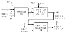
図2を参照すると、本発明の幾つかの実施形態による信頼性に基づく調節回路200の1つの実施態様が示されている。信頼性に基づく調節回路200は、データ処理回路100の信頼性モニター回路160の代わりに用いることができる。信頼性に基づく調節回路200は、検出出力(図示せず)の一部として受信された軟データ203を信頼性しきい値205と比較するように動作可能な比較器回路210を備える。幾つかの場合には、信頼性しきい値205はユーザープログラマブルである。他の場合には、信頼性しきい値205は固定値である。軟データ203のインスタンスが信頼性しきい値205未満である場合、比較器出力220はハイにアサートされる。対照的に、軟データ203のインスタンスが信頼性しきい値205以上である場合、比較器出力220はローにアサートされる。比較器出力220がハイにアサートされる(軟データ203のインスタンスに対応する)各クロック周期において、プロキシエラーカウンター回路230がインクリメントする。プロキシエラーカウンター回路230からのカウントは、パラメーター修正制御回路250に与えられるプロキシエラーカウント225である。
Referring to FIG. 2, one implementation of a reliability based
パラメーター修正制御回路250は、更新済みパラメーター260として最初に与えられる初期パラメーター値240を受信する。更新済みパラメーター260は、データ処理回路内の1つ又は複数の機能の動作を統御するパラメーターとして与えられる。幾つかの例として、更新済みパラメーター260は、可変利得増幅器の利得、アナログフィルターの遮断周波数及び/若しくはブースト、DCループオフセット、ターゲット、データ検出器回路によって用いられる検出器パラメーター、並びに/又はデータ復号化器回路によって用いられる復号化器パラメーターとすることができるが、これらに限定されるものではない。本明細書において提供される開示に基づくと、当業者であれば、パラメーター修正制御回路250によって調整することができる種々のパラメーターを認識するであろう。
The parameter
本発明の1つの特定の実施形態では、パラメーター修正制御回路250は、規定されたデータ処理期間数の間、初期パラメーター240を更新済みパラメーター260として用い続けることを可能にする。初期パラメーター240は、事前にプログラムされたデフォルト値とすることができる。その期間が完了すると、プロキシエラーカウント225が格納され、パラメーター修正回路250は、更新済みパラメーター260として与えられる新たな値を選択し、プロキシエラーカウンター回路230は、リセット信号223のアサートによってリセットされる。データ処理は、再び、更新パラメーター260の新たに選択された値を用いて規定された期間数の間、実行できるようになる。このプロセスは、更新済みパラメーター260の全ての可能な値がテストされると完了する。最後に、更新済みパラメーター260がいかなる回路を制御していようとも、最小のプロキシエラーカウント225を与えた更新済みパラメーター260の値が、その回路の調節されたパラメーターとして選択される。このプロセスは、以下の疑似コードに示されている。
/* 初期パラメーター値をテストする
初期パラメーター240を更新済みパラメーター260として選択する;
リセット225をアサートする;
リセット225をデアサートする;
For(i=0〜テスト期間の終了)
{
If(軟データ[i]203<信頼性しきい値205)
{
プロキシエラーカウント225+=1
}
}
パラメーターエラーカウント=プロキシエラーカウント225;
パラメーター値=初期パラメーター240;
/* 全ての他のパラメーター値をテストする */
リセット225をアサートする;
リセット225をデアサートする;
For(更新済みパラメーター260の各値)
{
更新済みパラメーター260の次の値を選択する;
For(i=0〜テスト期間の終了)
{
If(軟データ[i]203<信頼性しきい値205)
{
プロキシエラーカウント225+=1
}
}
If(プロキシエラーカウント225<パラメーターエラーカウント)
{
パラメーターエラーカウント=プロキシエラーカウント225;
パラメーター値=選択された次の値;
}
}
パラメーター値を選択する
In one particular embodiment of the present invention, the parameter
/ * Select
Assert reset 225;
Deassert reset 225;
For (i = 0 to end of test period)
{
If (soft data [i] 203 <reliability threshold 205)
{
}
}
Parameter error count =
Parameter value =
/ * Test all other parameter values * /
Assert reset 225;
Deassert reset 225;
For (each value of the updated parameter 260)
{
Select the next value of the updated parameter 260;
For (i = 0 to end of test period)
{
If (soft data [i] 203 <reliability threshold 205)
{
}
}
If (
{
Parameter error count =
Parameter value = next value selected;
}
}
Select parameter values
更に他の場合には、パラメーター修正制御回路250は、プロキシエラーカウント225が、規定しきい値未満になるまで検索を制限することによってパラメーター検索を制限するように修正することができる。規定しきい値未満のプロキシエラーカウント225を与えるパラメーター値が見つかると、そのパラメーター値が選択され、パラメーター検索プロセスは完了する。そのような場合、規定しきい値は、値をプログラマブル又は固定とすることができる。このプロセスは、以下の疑似コードで示される。
/* 初期パラメーター値をテストする
初期パラメーター240を更新済みパラメーター260として選択する;
リセット225をアサートする;
リセット225をデアサートする;
For(i=0〜テスト期間の終了)
{
If(軟データ[i]203<信頼性しきい値205)
{
プロキシエラーカウント225+=1
}
}
If(プロキシエラーカウント<規定しきい値)
{
更新済みパラメーター260=初期パラメーター240;
プロセスを終了する
Else
{
パラメーターエラーカウント=プロキシエラーカウント225;
パラメーター値=初期パラメーター240;
}
/* 規定しきい値が達成されるまで他のパラメーター値をテストする */
リセット225をアサートする;
リセット225をデアサートする;
For(更新済みパラメーター260の各値)
{
更新済みパラメーター260の次の値を選択する;
For(i=0〜テスト期間の終了)
{
If(軟データ[i]203<信頼性しきい値205)
{
プロキシエラーカウント225+=1
}
}
If(プロキシエラーカウント<規定しきい値)
{
更新済みパラメーター260=選択された次の値;
プロセスを終了
}
Else If(プロキシエラーカウント225<パラメーターエラーカウント)
{
パラメーターエラーカウント=プロキシエラーカウント225;
パラメーター値=選択された次の値;
}
}
In yet other cases, the parameter
/ * Select
Assert reset 225;
Deassert reset 225;
For (i = 0 to end of test period)
{
If (soft data [i] 203 <reliability threshold 205)
{
}
}
If (proxy error count <specified threshold)
{
Updated parameter 260 =
Else that terminates the process
{
Parameter error count =
Parameter value =
}
/ * Test other parameter values until specified threshold is achieved * /
Assert reset 225;
Deassert reset 225;
For (each value of the updated parameter 260)
{
Select the next value of the updated parameter 260;
For (i = 0 to end of test period)
{
If (soft data [i] 203 <reliability threshold 205)
{
}
}
If (proxy error count <specified threshold)
{
Updated parameter 260 = next value selected;
End process}
Else If (
{
Parameter error count =
Parameter value = next value selected;
}
}
更に他の場合には、更新済みパラメーター260の全て値をテストする必要がないようなより高機能な(sophiscated)テストプロセスを用いることができる。そのようなストリームラインテストプロセスは、以下の図5及び図6に関して以下で論述するものと一致して行うことができる。そのような場合には、パラメーター修正制御回路250の動作は、更新済みパラメーター260の許容可能な値を特定するストリームライン手法を用いるように修正することができる。図5及び図6に関して以下で論述する方法は、既知データセットから取り出された実際のエラーカウントに基づく種々のパラメーター値を検索するように修正することができることに留意されたい。そのような手法は、図8〜図10に関して以下で論述される。
In still other cases, a more sophisticated test process can be used that does not require testing all the values of the updated parameter 260. Such a streamline test process can be performed consistent with that discussed below with respect to FIGS. 5 and 6 below. In such a case, the operation of the parameter
図3を参照すると、本発明の1つ又は複数の実施形態による信頼性データに基づく調節回路部を有する読取りチャネル回路310を備えるストレージデバイス300が示されている。ストレージシステム300は、例えば、ハードディスクドライブとすることができる。ストレージシステム300はまた、前置増幅器370と、インターフェースコントローラー320と、ハードディスクコントローラー366と、モーターコントローラー368と、スピンドルモーター372と、ディスクプラッター378と、読取り/書込みヘッドアセンブリ376とを備える。インターフェースコントローラー320は、ディスクプラッター378へ/からのデータのアドレス指定及びタイミングを制御する。ディスクプラッター378上のデータは、読取り/書込みヘッドアセンブリ376がディスクプラッター378の上方で適切に位置決めされたときに該アセンブリが検出することができる磁気信号の群からなる。1つの実施形態では、ディスクプラッター378は、水平記録方式又は垂直記録方式のいずれかに従って記録された磁気信号を含む。
Referring to FIG. 3, a
通常の読取り動作では、読取り/書込みヘッドアセンブリ376は、モーターコントローラー368によってディスクプラッター378上の所望のデータトラックの上方に正確に位置決めされる。モーターコントローラー368は、ディスクプラッター378に対して読取り/書込みヘッドアセンブリ376の位置決めも行うし、ハードディスクコントローラー366の指示のもとでディスクプラッター378上の適切なデータトラックに読取り/書込みヘッドアセンブリを移動させることによってスピンドルモーター372の駆動も行う。スピンドルモーター372は、定められたスピン速度(RPM)でディスクプラッター378をスピンさせる。読取り/書込みヘッドアセンブリ378が適切なデータトラックに隣接して位置決めされると、ディスクプラッター378がスピンドルモーター372によって回転されながら、ディスクプラッター378上のデータを表す磁気信号が読取り/書込みヘッドアセンブリ376によって検知される。検知された磁気信号は、ディスクプラッター378上の磁気データを表す連続した微小アナログ信号として与えられる。この微小アナログ信号は、読取り/書込みヘッドアセンブリ376から前置増幅器370を介して読取りチャネル回路310に転送される。前置増幅器370は、ディスクプラッター378からアクセスされた微小アナログ信号を増幅するように動作可能である。次に、読取りチャネル回路310は、受信したアナログ信号を復号化及びデジタル化して、ディスクプラッター378に元々書き込まれていた情報を再生する。このデータは、読取りデータ303として受信回路に与えられる。書込み動作は、先行する読取り動作の実質的に逆であり、書込みデータ301が読取りチャネル回路310に与えられる。このデータは、その後、符号化され、ディスクプラッター378に書き込まれる。
In a normal read operation, the read /
テスト動作中、又は幾つかの場合には標準的なデータ読取り動作中、信頼性データに基づく調節制御回路部は、読取りチャネル回路310の動作を統御する1つ又は複数のパラメーターを修正し、信頼性しきい値が満たされるか否かを監視し続ける。このように、読取りチャネル回路310内のパラメーターを修正して、読取りチャネル回路310の性能を改善することができる。信頼性データに基づく調節制御回路部を備える処理回路は、図1及び図2に関して上記で論述したものと同様に実施することができ、かつ/又は図5、図6、及び/若しくは図7に関して以下で論述するものと同様に動作することができる。他の場合には、信頼性データに基づく調節制御回路部は、図5及び図6に関して以下で論述するものと同様のストリームライン検索を用いる図8に関して以下で論述するものと同様の既知データに基づく調節制御回路部によって置き換えることができる。 During a test operation, or in some cases a standard data read operation, the adjustment control circuitry based on the reliability data modifies one or more parameters that govern the operation of the read channel circuit 310 to Continue to monitor whether the sex threshold is met. In this way, parameters in the read channel circuit 310 can be modified to improve the performance of the read channel circuit 310. The processing circuit comprising the adjustment control circuitry based on the reliability data can be implemented in a manner similar to that discussed above with respect to FIGS. 1 and 2 and / or with respect to FIGS. 5, 6, and / or 7. It can operate in the same way as discussed below. In other cases, the adjustment control circuitry based on the reliability data may generate known data similar to that discussed below with respect to FIG. 8 using a streamline search similar to that discussed below with respect to FIGS. It can be replaced by an adjustment control circuit unit based.
ストレージシステムは、SATA、SAS又は当該技術分野において知られている他のストレージ技術を利用することができることに留意すべきである。また、ストレージシステム300は、例えばRAID(低価格ディスク冗長アレイ又は独立ディスク冗長アレイ)に基づくストレージシステム等のより大きなストレージシステムに統合することができることにも留意すべきである。ストレージシステム300の様々な機能又はブロックをソフトウェア又はファームウェアのいずれかに実装することができる一方、他の機能又はブロックはハードウェアに実装されることにも留意すべきである。
It should be noted that the storage system can utilize SATA, SAS or other storage technologies known in the art. It should also be noted that the
図4を参照すると、本発明の幾つかの実施形態による信頼性データに基づく調節回路部を有する受信機420を備えるデータ伝送システム400が示されている。データ伝送システム400は、当該技術分野において知られているような転送媒体430を介して符号化された情報を送信するように動作可能な送信機410を備える。符号化されたデータは、受信機420によって転送媒体430から受信される。受信機420は、信頼性データに基づく調節回路部を組み込んでいる。受信されたデータを処理している間、受信されたデータは、アナログ信号から一連の対応するデジタルサンプルに変換され、デジタルサンプルは等化されて、等化出力が得られる。等化出力は、次に、データ検出器回路とデータ復号化器回路との双方を備えるデータ処理回路に与えられる。データは、異なるデータセットに適用される処理反復回数間の変動を許容する中央メモリを介してデータ復号化器とデータ検出器回路との間で伝達される。転送媒体430は、当該技術分野において知られているような任意の転送媒体とすることができることに留意すべきである。任意の転送媒体には、無線媒体、光媒体、又は有線媒体が含まれるが、これらに限定されるものではない。本明細書において提供される開示に基づくと、当業者であれば、本発明の異なる実施形態に関して用いることができる種々の転送媒体を認識するであろう。
Referring to FIG. 4, a
テスト動作中、又は幾つかの場合には標準的なデータ読取り動作中、信頼性データに基づく調節制御回路部は、受信機420の動作を統御する1つ又は複数のパラメーターを修正し、信頼性しきい値が満たされるか否かを監視し続ける。このように、受信機420内のパラメーターを修正して受信機420の性能を改善することができる。信頼性データに基づく調節制御回路部を備える処理回路は、図1及び図2に関して上記で論述したものと同様に実施することができ、かつ/又は図5、図6及び/若しくは図7に関して以下で論述するものと同様に動作することができる。他の場合には、信頼性データに基づく調節制御回路部は、図5及び図6に関して以下で論述するものと同様のストリームライン検索を用いる図8に関して以下で論述するものと同様の既知データに基づく調節制御回路部によって置き換えることができる。 During a test operation, or in some cases a standard data read operation, the adjustment control circuitry based on the reliability data modifies one or more parameters that govern the operation of the receiver 420 to improve reliability. Continue to monitor whether the threshold is met. In this way, parameters within the receiver 420 can be modified to improve the performance of the receiver 420. The processing circuit comprising the adjustment control circuitry based on the reliability data can be implemented in a manner similar to that discussed above with respect to FIGS. 1 and 2 and / or with respect to FIGS. 5, 6 and / or 7 below. Can operate in the same way as discussed in. In other cases, the adjustment control circuitry based on the reliability data may generate known data similar to that discussed below with respect to FIG. 8 using a streamline search similar to that discussed below with respect to FIGS. It can be replaced by an adjustment control circuit unit based.
図5を参照すると、流れ図500が、本発明の様々な実施形態による信頼性に基づくパラメーター調節のための方法を示している。流れ図500に従って、初期パラメーターが検索のために選択される(ブロック505)。選択されたパラメーターは、データ処理回路の或る部分の動作を統御する任意のパラメーターとすることができる。幾つかの例として、パラメーターは、可変利得増幅器の利得、アナログフィルターの遮断周波数及び/若しくはブースト、DCループオフセット、ターゲット、データ検出器回路によって用いられる検出器パラメーター、並びに/又はデータ復号化器回路によって用いられる復号化器パラメーターとすることができるが、これらに限定されるものではない。本明細書において提供される開示に基づくと、当業者であれば、図5の方法によって調整することができる種々のパラメーターを認識するであろう。選択されたパラメーターの現在の値が読み取られ、変数PARAMとして格納される(ブロック510)。更新済みパラメーター(すなわち、データ処理回路に適用されるパラメーター)は、現在の値と等しく設定され、該更新済みパラメーターは、データ処理回路に適用される(ブロック515)。更新済みパラメーターを処理回路に適用することは、更新済みパラメーターを用いて或る期間の間、処理回路を動作させることを含む。この処理が行われるとき、データ検出器回路からの軟データの幾つのインスタンスが、規定しきい値未満であるのかのカウントが行われ、プロキシエラーカウントが得られる。この処理が行われると、プロキシエラーカウントが読み取られ、変数COUNTとして格納される(ブロック520)。その後、プロキシエラーカウント値はリセットされる。
Referring to FIG. 5, a
次に、選択されたパラメーターの別の値がテストされずに残っているか否かが判断される(ブロック530)。別の値がテストされずに残っている場合(ブロック530)、検索方向が計算される(ブロック600)。検索方向を選択するこのプロセスは、図6に関して以下でより詳細に論述される。検索方向が特定されると(ブロック600)、更新済みパラメーターの値が検索方向及びステップサイズに基づいて計算される(ブロック535)。幾つかの場合には、ステップサイズはユーザープログラマブルとすることができる一方、他の場合には、ステップサイズは固定とすることができる。本発明の幾つかの実施形態では、更新済みパラメーターの値は、以下の疑似コードに従って計算される。
If(検索方向は正である)
{
更新済みパラメーター=更新済みパラメーター+ステップサイズ
}
Else
{
更新済みパラメーター=更新済みパラメーター−ステップサイズ
}
次に、この新たな更新済みパラメーターは、データ処理回路に適用される(ブロック540)。更新済みパラメーターを処理回路に適用することは、更新済みパラメーターを用いて或る期間の間、処理回路を動作させることを含む。この処理が行われるとき、データ検出器回路からの軟データの幾つのインスタンスが規定しきい値未満であるのかのカウントが行われ、プロキシエラーカウントが得られる。処理が行われると、プロキシエラーカウントが読み取られ、変数NEXT_COUNTとして格納される(ブロック545)。その後、プロキシエラーカウント値はリセットされる。
Next, it is determined whether another value for the selected parameter remains untested (block 530). If another value remains untested (block 530), the search direction is calculated (block 600). This process of selecting the search direction is discussed in more detail below with respect to FIG. Once the search direction is identified (block 600), the value of the updated parameter is calculated based on the search direction and step size (block 535). In some cases, the step size can be user programmable, while in other cases, the step size can be fixed. In some embodiments of the invention, the value of the updated parameter is calculated according to the following pseudo code:
If (search direction is positive)
{
Updated parameter = updated parameter + step size}
Else
{
Updated parameter = updated parameter-step size}
This new updated parameter is then applied to the data processing circuit (block 540). Applying the updated parameter to the processing circuit includes operating the processing circuit for a period of time using the updated parameter. When this process is performed, a count is made of how many instances of the soft data from the data detector circuit are below a specified threshold, resulting in a proxy error count. Once processed, the proxy error count is read and stored as the variable NEXT_COUNT (block 545). Thereafter, the proxy error count value is reset.
NEXT_COUNTの値がCOUNTの値以下であるか否かが判断される(ブロック550)。NEXT_COUNTの値がCOUNTの値以下である場合(ブロック550)、変数COUNTは、NEXT_COUNTの値と等しく設定され、PARAMの値は、更新済みパラメーターの値と等しく設定される(ブロック555)。ブロック530、600、535、540、545、550、555のプロセスは、選択されたパラメーターの全ての値がテストされるまで繰り返す。
It is determined whether the value of NEXT_COUNT is less than or equal to the value of COUNT (block 550). If the value of NEXT_COUNT is less than or equal to the value of COUNT (block 550), the variable COUNT is set equal to the value of NEXT_COUNT, and the value of PARAM is set equal to the value of the updated parameter (block 555). The process of
テストされる、選択されたパラメーターの値がなくなると(ブロック530)、又はNEXT_COUNTの値がCOUNTの値よりも大きい場合(ブロック550)、選択されたパラメーターの許容可能な値が変数PARAMに格納済みであり、その値は、データ処理回路に適用される(ブロック560)。次に、データ処理回路の別のパラメーターがテストされずに残っているか否かが判断される(ブロック565)。別のパラメーターがテストされずに残っている場合(ブロック565)、テストされる次のパラメーターが選択され(ブロック575)、ブロック510〜565(ブロック600を含む)のプロセスが、新たに選択されたパラメーターに対して繰り返される。そうではなく、テストされずに残っている他のパラメーターがない場合(ブロック565)、テストプロセスは終了する(ブロック570)。 If the value of the selected parameter to be tested runs out (block 530) or the value of NEXT_COUNT is greater than the value of COUNT (block 550), the acceptable value of the selected parameter is stored in the variable PARAM And the value is applied to the data processing circuit (block 560). Next, it is determined whether another parameter of the data processing circuit remains untested (block 565). If another parameter remains untested (block 565), the next parameter to be tested is selected (block 575) and the process of blocks 510-565 (including block 600) is newly selected. Repeated for parameters. Otherwise, if there are no other parameters left untested (block 565), the test process ends (block 570).
図6を参照すると、流れ図600が、検索方向を確定するための、本発明の幾つかの実施形態による方法を示している。流れ図600は、図5からの同じ番号のブロックの方法を概説している。流れ図600に従って、更新済みパラメーターが流れ図500のプロセスから受信される(ブロック602)。更新済みパラメーターの次の値(すなわち、規定量だけ増加された更新済みパラメーターの値)が選択される(ブロック605)。更新済みパラメーターの次の値は、データ処理回路に適用される(ブロック610)。更新済みパラメーターの次の値を処理回路に適用することは、更新済みパラメーターを用いて或る期間の間、処理回路を動作させることを含む。この処理が行われるとき、データ検出器回路からの軟データの幾つのインスタンスが規定しきい値未満であるのかのカウントが行われ、プロキシエラーカウントが得られる。この処理が行われると、プロキシエラーカウントが読み取られ、変数PLUS_COUNTとして格納される(ブロック520)。その後、プロキシエラーカウント値はリセットされる。
Referring to FIG. 6, a
次に、更新済みパラメーターの前の値(すなわち、規定量だけ減少された更新済みパラメーターの値)が選択される(ブロック620)。更新済みパラメーターの前の値がデータ処理回路に適用される(ブロック625)。更新済みパラメーターの前の値を処理回路に適用することは、更新済みパラメーターを用いて或る期間の間、処理回路を動作させることを含む。この処理が行われるとき、データ検出器回路からの軟データの幾つのインスタンスが規定しきい値未満であるのかのカウントが行われ、プロキシエラーカウントが得られる。処理が行われると、プロキシエラーカウントが読み取られ、変数MINUS_COUNTとして格納される(ブロック630)。その後、プロキシエラーカウント値はリセットされる。 Next, the previous value of the updated parameter (ie, the value of the updated parameter that has been reduced by a specified amount) is selected (block 620). The previous value of the updated parameter is applied to the data processing circuit (block 625). Applying the previous value of the updated parameter to the processing circuit includes operating the processing circuit for a period of time using the updated parameter. When this process is performed, a count is made of how many instances of the soft data from the data detector circuit are below a specified threshold, resulting in a proxy error count. Once processed, the proxy error count is read and stored as a variable MINUS_COUNT (block 630). Thereafter, the proxy error count value is reset.
次に、PLUS_COUNTの値がMINUS_COUNTの値よりも大きいか否かが判断される(ブロック635)。PLUS_COUNTの値がMINUS_COUNTの値よりも大きい場合(ブロック635)、検索方向は、負と等しく設定される(ブロック650)。そうでない場合、検索方向は正と等しく設定される(ブロック640)。次に、検索方向は、図5のプロセスについて用いるために返される(ブロック660)。 Next, it is determined whether the value of PLUS_COUNT is greater than the value of MINUS_COUNT (block 635). If the value of PLUS_COUNT is greater than the value of MINUS_COUNT (block 635), the search direction is set equal to negative (block 650). Otherwise, the search direction is set equal to positive (block 640). The search direction is then returned for use with the process of FIG. 5 (block 660).
図7を参照すると、流れ図700が本発明の幾つかの実施形態による信頼性に基づくパラメーター調節のための別の方法を示している。流れ図700に従って、初期パラメーターが検索のために選択される(ブロック705)。選択されたパラメーターは、データ処理回路の或る部分の動作を統御する任意のパラメーターとすることができる。幾つかの例として、パラメーターは、可変利得増幅器の利得、アナログフィルターの遮断周波数及び/若しくはブースト、DCループオフセット、ターゲット、データ検出器回路によって用いられる検出器パラメーター、並びに/又はデータ復号化器回路によって用いられる復号化器パラメーターとすることができるが、これらに限定されるものではない。本明細書において提供される開示に基づくと、当業者であれば、図7の方法によって調整することができる種々のパラメーターを認識するであろう。選択されたパラメーターの現在の値が読み取られ、変数PARAMとして格納される(ブロック710)。更新済みパラメーター(すなわち、データ処理回路に適用されるパラメーター)は、現在の値と等しく設定され(ブロック715)、該更新済みパラメーターは、データ処理回路に適用される(ブロック720)。更新済みパラメーターを処理回路に適用することは、更新済みパラメーターを用いて或る期間の間、処理回路を動作させることを含む。この処理が行われるとき、データ検出器回路からの軟データの幾つのインスタンスが規定しきい値未満であるのかのカウントが行われ、プロキシエラーカウントが得られる。この処理が行われると、プロキシエラーカウントが読み取られ、変数COUNTとして格納される(ブロック725)。その後、プロキシエラーカウント値はリセットされる。
Referring to FIG. 7, a
次に、選択されたパラメーターの別の値がテストされずに残っているか否かが判断される(ブロック730)。別の値がテストされずに残っている場合(ブロック730)、更新済みパラメーターの次の値が選択される(ブロック735)。次に、この新たな更新済みパラメーターは、データ処理回路に適用される(ブロック740)。更新済みパラメーターを処理回路に適用することは、更新済みパラメーターを用いて或る期間の間、処理回路を動作させることを含む。この処理が行われるとき、データ検出器回路からの軟データの幾つのインスタンスが規定しきい値未満であるのかのカウントが行われ、プロキシエラーカウントが得られる。この処理が行われると、プロキシエラーカウントが読み取られ、変数NEXT_COUNTとして格納される(ブロック745)。その後、プロキシエラーカウント値はリセットされる。 Next, it is determined whether another value of the selected parameter remains untested (block 730). If another value remains untested (block 730), the next value of the updated parameter is selected (block 735). This new updated parameter is then applied to the data processing circuit (block 740). Applying the updated parameter to the processing circuit includes operating the processing circuit for a period of time using the updated parameter. When this process is performed, a count is made of how many instances of the soft data from the data detector circuit are below a specified threshold, resulting in a proxy error count. Once this processing is done, the proxy error count is read and stored as a variable NEXT_COUNT (block 745). Thereafter, the proxy error count value is reset.
NEXT_COUNTの値がCOUNTの値以下であるか否かが判断される(ブロック750)。NEXT_COUNTの値がCOUNTの値以下である場合(ブロック750)、変数COUNTは、NEXT_COUNTの値と等しく設定され、PARAMの値は、更新済みパラメーターの値と等しく設定される(ブロック755)。ブロック730〜755のプロセスは、選択されたパラメーターの全ての値がテストされるまで繰り返す。 It is determined whether the value of NEXT_COUNT is less than or equal to the value of COUNT (block 750). If the value of NEXT_COUNT is less than or equal to the value of COUNT (block 750), the variable COUNT is set equal to the value of NEXT_COUNT, and the value of PARAM is set equal to the value of the updated parameter (block 755). The process of blocks 730-755 is repeated until all values of the selected parameter have been tested.
選択されたパラメーターの値の全てがテストされると(ブロック730)、選択されたパラメーターの最良の利用可能な値が変数PARAMに格納され、その値は、データ処理回路に適用される(ブロック760)。次に、データ処理回路の別のパラメーターがテストされずに残っているか否かが判断される(ブロック765)。別のパラメーターがテストされずに残っている場合(ブロック765)、テストされる次のパラメーターが選択され(ブロック775)、ブロック710〜765のプロセスが、新たに選択されたパラメーターに対して繰り返される。そうではなく、テストされずに残っている他のパラメーターがない場合(ブロック765)、テストプロセスは終了する(ブロック770)。 When all of the values of the selected parameter have been tested (block 730), the best available value of the selected parameter is stored in the variable PARAM and that value is applied to the data processing circuit (block 760). ). Next, it is determined whether another parameter of the data processing circuit remains untested (block 765). If another parameter remains untested (block 765), the next parameter to be tested is selected (block 775) and the process of blocks 710-765 is repeated for the newly selected parameter. . Otherwise, if there are no other parameters left untested (block 765), the test process ends (block 770).
図8は、本発明の1つ又は複数の実施形態によるストリームライン検索を有する既知データに基づくモニター回路860を備えるデータ処理回路800を示している。データ処理回路800は、アナログ処理回路808を備える。アナログ処理回路808は、アナログフロントエンド回路810と、タイミング及び制御をアナログフロントエンド回路810に提供するように動作可能なフロントエンド処理ループ811と、ターゲットに基づくフィルタリングフィードバックをアナログフロントエンド回路810に提供するように動作可能なターゲット回路809とを備える。アナログフロントエンド回路810は、当該技術分野において知られているようなアナログフィルター及び増幅器回路を含むことができるが、これらに限定されるものではない。本明細書において提供される開示に基づくと、当業者であれば、アナログフロントエンド回路810の一部として含めることができる種々の回路部を認識するであろう。幾つかの場合には、アナログフロント回路810の一部として含まれる可変利得増幅器の利得を修正可能とすることができ、アナログフロントエンド回路810に含まれるアナログフィルターの遮断周波数及びブーストを修正可能とすることができる。フロントエンド処理ループ811は、当該技術分野において知られているアナログフロントエンド回路810にタイミングを提供するように動作可能な任意の処理ループとすることができる。幾つかの場合には、そのようなフロントエンド処理ループ811は、修正可能とすることができるDCループオフセットを含む。ターゲット回路809は、当該技術分野において知られている任意の、ターゲットに基づくフィルター回路とすることができる。様々な場合において、ターゲット回路809によって用いられるターゲットは修正可能とすることができる。本明細書において提供される開示に基づくと、当業者であれば、本発明の異なる実施形態に関して用いることができる種々の、ターゲットに基づくフィルター回路及びフロントエンド処理ループを認識するであろう。
FIG. 8 illustrates a data processing circuit 800 comprising a monitor circuit 860 based on known data with streamline search according to one or more embodiments of the present invention. The data processing circuit 800 includes an
アナログフロントエンド回路810は、アナログ信号805を受信する。アナログフロントエンド回路810は、アナログ信号805を処理し、処理済みのアナログ信号812(112)をアナログ/デジタル変換器回路814に提供する。幾つかの場合には、アナログ信号805は、ストレージ媒体(図示せず)に対して配置される読取り/書込みヘッドアセンブリ(図示せず)から取り出される。他の場合には、アナログ信号805は、伝送媒体(図示せず)からの信号を受信するように動作可能な受信機回路(図示せず)から取り出される。伝送媒体は、有線又は無線とすることができる。本明細書において提供される開示に基づくと、当業者であれば、アナログ入力805を取り出すことができる種々の信号源を認識するであろう。
The analog front end circuit 810 receives the
アナログ/デジタル変換器回路814は、処理済みのアナログ信号812を対応する一連のデジタルサンプル816に変換する。アナログ/デジタル変換器回路814は、アナログ入力信号に対応するデジタルサンプルを生成することが可能な、当該技術分野において知られている任意の回路とすることができる。本明細書において提供される開示に基づくと、当業者であれば、本発明の異なる実施形態に関して用いることができる種々のアナログ/デジタル変換器回路を認識するであろう。デジタルサンプル816は等化器回路820に与えられる。等化器回路820は、デジタルサンプル816に等化アルゴリズムを適用して、等化出力825を得る。本発明の幾つかの実施形態では、等化器回路820は、当該技術分野において知られているようなデジタル有限インパルス応答フィルター回路である。等化出力825は、データ検出器回路830に与えられる。幾つかの場合には、等化器820は、データ検出器回路830が処理に利用可能になるまで1つ又は複数の符号語を保持するのに十分なメモリを備える。
The analog /
データ検出器回路830は、受信した符号語又はデータセットにデータ検出アルゴリズムを適用するように動作可能であり、幾つかの場合には、データ検出器回路830は、2つ以上の符号語を並列に処理することができる。本発明の幾つかの実施形態では、データ検出器回路830は、当該技術分野において知られているようなビタビアルゴリズムデータ検出器回路である。本発明の他の実施形態では、データ検出器回路830は、当該技術分野において知られているような最大事後データ検出器回路である。本明細書において提供される開示に基づくと、当業者であれば、本発明の異なる実施形態に関して用いることができる種々のデータ検出器回路を認識するであろう。データ検出器回路830は、等化器回路820又は中央メモリ回路850からのデータセットが利用可能であることに基づいて始動される。 The data detector circuit 830 is operable to apply a data detection algorithm to the received codeword or data set, and in some cases, the data detector circuit 830 parallels two or more codewords. Can be processed. In some embodiments of the present invention, the data detector circuit 830 is a Viterbi algorithm data detector circuit as is known in the art. In other embodiments of the present invention, the data detector circuit 830 is a maximum a posteriori data detector circuit as is known in the art. Based on the disclosure provided herein, one of ordinary skill in the art will recognize a variety of data detector circuits that can be used in connection with different embodiments of the present invention. Data detector circuit 830 is triggered based on the availability of a data set from equalizer circuit 820 or central memory circuit 850.
完了すると、データ検出器回路830は検出器出力895を与える。検出出力895は局所インターリーバー回路842及び既知データに基づくモニター回路860に与えられる。局所インターリーバー回路842は、検出出力として含まれるデータセットの副部分(すなわち局所チャンク)をシャッフルするように動作可能であり、インターリーブされた符号語846を与え、該インターリーブされた符号語846は中央メモリ回路850に格納される。インターリーバー回路842は、データセットをシャッフルして再配列されたデータセットを得ることが可能な、当該技術分野において知られている任意の回路とすることができる。インターリーブされた符号語846は中央メモリ回路850に格納される。
Upon completion, the data detector circuit 830 provides a
データ復号化器回路870が利用可能になると、以前に格納されたインターリーブされた符号語846が、復号化器入力852として中央メモリ回路850からアクセスされ、当該技術分野において知られているように大域的にインターリーブされ、データ復号化アルゴリズムが適用される。本発明の幾つかの実施形態では、データ復号化アルゴリズムは当該技術分野において知られているような低密度パリティチェックアルゴリズムである。本明細書において提供される開示に基づくと、当業者であれば、本発明の異なる実施形態に関して用いることができる他の復号化アルゴリズムを認識するであろう。データ復号化アルゴリズムが所与のデータセットに対して完了すると、復号化アルゴリズムが収束した(すなわち、結果のデータセットが、パリティエラーがないことによって示されるように、最初に書き込まれたデータと一致する)か否かが判断される。復号化アルゴリズムが収束したと判断された場合、その結果の復号化データセットは硬判定出力872としてデインターリーバー回路880に与えられる。デインターリーバー回路880は、データを再配列して、データに適用された大域インターリーブ及び局所インターリーブの双方を逆に行い、デインターリーブされた出力882を得る。デインターリーブされた出力882は硬判定出力回路890に与えられる。硬判定出力回路890は、順序がばらばらで完了する場合があるデータセットを再順序付けし、該データセットの元の順序に戻すように動作可能である。次に、元の順序付けされたデータセットは硬判定出力892として与えられる。
When the
代替的に、データ復号化アルゴリズムが収束しなかったと判断された(すなわち、パリティエラーが残っている)場合、完了したデータセットは、当該技術分野において知られているように大域的にデインターリーブされ、復号化器出力854として中央メモリ回路850に再び書き込まれる。データ検出器回路830が利用可能になると、以前に格納され復号化器出力848が、中央メモリ回路850からアクセスされ、デインターリーバー回路844によって局所的にデインターリーブされる。デインターリーバー回路844は、インターリーバー回路842によって最初に実行されたシャフルを逆に行うように復号化器出力848を再配列する。その結果のデインターリーブされた出力897は、データ検出器回路830に与えられる。
Alternatively, if it is determined that the data decoding algorithm has not converged (ie, a parity error remains), the completed data set is globally deinterleaved as is known in the art. And is written back to the central memory circuit 850 as the
幾つかの場合には、既知データに基づくモニター回路860は、テスト/調節期間中にのみ動作する。他の場合には、既知データに基づくモニター回路860は、連続的に動作される。既知データに基づくモニター回路860は、検出器出力895を受信し、データ処理回路800の動作を統御するのに用いられる1つ又は複数のパラメーターを修正する。パラメーターは、入出力864を介してアナログ処理回路808に通信することができ、入出力862を介してデータ検出器回路830に通信することができ、かつ/又は入出力866を介してデータ復号化器回路870に通信することができる。パラメーターは、アナログフロントエンド回路810に含まれる可変利得増幅器の利得、アナログフロントエンド回路810に含まれるアナログフィルターの遮断周波数及び/若しくはブースト、フロントエンド処理ループ811のDCループオフセット、ターゲット回路809によって用いられるターゲット、データ検出器回路830によって用いられる検出器パラメーター、並びに/又はデータ復号化器回路870によって用いられる復号化器パラメーターとすることができるが、これらに限定されるものではない。本明細書において提供される開示に基づくと、当業者であれば、本発明の異なる実施形態による既知データに基づくモニター回路860によって調整することができる種々のパラメーターを認識するであろう。
In some cases, the monitor circuit 860 based on known data operates only during the test / adjustment period. In other cases, the monitor circuit 860 based on known data is operated continuously. A monitor circuit 860 based on known data receives the
既知データに基づくモニター回路860は、硬判定出力892を既知データセット868と比較する。データが処理されているとき、既知データに基づくモニター回路860は、入出力862、入出力864及び入出力866を介してそれぞれの回路に与えられる1つ又は複数のパラメーターの値(複数の場合もあり)を選択する。次に、データが、或る時間期間にわたって、選択されたパラメーター値を用いてデータ処理回路800を通じて処理される。硬判定出力892のインスタンスが既知データセット868の対応するインスタンスと等しくないと、既知データに基づくモニター回路860が判断した場合、エラーが示される。このエラーはエラーレートに組み込まれる。エラーレートが規定しきい値を超えた場合、1つ又は複数のパラメーターの1つ又は複数の新たな値が選択され、許容可能なパラメーターが特定されるまで、再テストプロセスが続く。図2に関して上記で論述したものと同様の回路を用いて、既知データに基づくモニター回路を実装することができる。異なる点は、図2の回路の比較器210が、軟データ203及び信頼性しきい値205の代わりに既知データセット868及び硬判定出力892を受信するということである。既知データに基づくモニター回路860は、図5及び図6に関して上記で論述したようなストリームラインパラメーター値検索プロセスを組み込む。
Monitor circuit 860 based on known data compares hard decision output 892 with known data set 868. When the data is being processed, the monitor circuit 860 based on the known data may have one or more parameter values (in some cases) provided to the respective circuits via the input / output 862, the input / output 864, and the input / output 866. Select Yes). The data is then processed through the data processing circuit 800 using the selected parameter value for a period of time. If monitor circuit 860 determines that the instance of hard decision output 892 is not equal to the corresponding instance of known data set 868, an error is indicated. This error is incorporated into the error rate. If the error rate exceeds a specified threshold, one or more new values of one or more parameters are selected and the retest process continues until an acceptable parameter is identified. A monitor circuit based on known data can be implemented using a circuit similar to that discussed above with respect to FIG. The difference is that the
上記のアプリケーションにおいて論述した様々なブロックは、他の機能とともに集積回路に実装することができることに留意すべきである。そのような集積回路は、所与のブロック、システム若しくは回路の機能の全て、又はブロック、システム若しくは回路のサブセットのみを含むことができる。また、ブロック、システム又は回路の要素を複数の集積回路にわたって実装することができる。そのような集積回路は、モノリシック集積回路、フリップチップ集積回路、マルチチップモジュール集積回路及び/又は混合信号集積回路を含むが、これらに限定されるものではない、当該技術分野において知られている任意のタイプの集積回路とすることができる。本明細書において論述されたブロック、システム又は回路の様々な機能を、ソフトウェア又はファームウェアのいずれかにおいて実装することができることにも留意すべきである。そのような幾つかの場合には、システム全体、ブロック全体又は回路全体を、そのソフトウェア等価物又はファームウェア等価物を用いて実装することができる。他の場合には、所与のシステム、ブロック又は回路の一部分をソフトウェア又はファームウェアにおいて実装することもできる一方、他の部分はハードウェアにおいて実装される。 It should be noted that the various blocks discussed in the above application can be implemented in an integrated circuit along with other functions. Such an integrated circuit may include all of the functions of a given block, system or circuit, or only a subset of the block, system or circuit. Also, block, system or circuit elements may be implemented across multiple integrated circuits. Such integrated circuits include any known in the art including, but not limited to, monolithic integrated circuits, flip chip integrated circuits, multichip module integrated circuits, and / or mixed signal integrated circuits. Type of integrated circuit. It should also be noted that the various functions of the blocks, systems or circuits discussed herein can be implemented in either software or firmware. In some such cases, the entire system, block or circuit can be implemented using its software equivalent or firmware equivalent. In other cases, portions of a given system, block, or circuit may be implemented in software or firmware, while other portions are implemented in hardware.
結論として、本発明はデータ処理のための新規なシステム、デバイス、方法及び構成を提供する。本発明の1つ又は複数の実施形態の詳細な説明が上記で与えられたが、本発明の趣旨から逸脱することなく、様々な代替形態、修正形態及び均等物が当業者には明らかであろう。したがって、上記の説明は本発明の範囲を限定するものとして解釈されるべきではなく、本発明の範囲は添付の特許請求の範囲によって画定される。 In conclusion, the present invention provides novel systems, devices, methods and configurations for data processing. While a detailed description of one or more embodiments of the invention has been given above, various alternatives, modifications, and equivalents will be apparent to those skilled in the art without departing from the spirit of the invention. Let's go. Therefore, the above description should not be taken as limiting the scope of the invention, which is defined by the appended claims.
図1
105 Analog Input アナログ入力
109 Target ターゲット
110 Analog Front End Circuit アナログフロントエンド回路
111 Front End Processing Loops フロントエンド処理ループ
114 Analog to Digital Converter Circuit アナログ/デジタル変換器回路
120 DFIR Circuit DFIR回路
130 Data Detector Circuit データ検出器回路
142 Local Interleaver Circuit 局所インターリーバー回路
144 Local De-Interleaver Circuit 局所デインターリーバー回路
150 Central Memory Circuit 中央メモリ回路
160 Reliability Monitor Circuit 信頼性モニター回路
168 Reliability Threshold 信頼性しきい値
169 Reset リセット
170 Data Decoder Circuit Including Global Interleaving/De-InterleavingCircuitry 大域的インターリーブ/デインターリーブ回路部を備えるデータ復号化器回路
180 De-Interleaver Circuit デインターリーバー回路
190 Hard Decision Output Circuit 硬判定出力回路
192 Hard Decision Output 硬判定出力
図2
203 Soft Data 軟データ
205 Reliability Threshold 信頼性しきい値
210 Comparator Circuit 比較器回路
223 Reset リセット
225 Proxy Error Count プロキシエラーカウント
230 Proxy Error Counter Circuit プロキシエラーカウンター回路
240 Initial Parameter 初期パラメーター
250 Parameter Modification Control Circuit パラメーター修正制御回路
260 Updated Parameter 更新済みパラメーター
図3
301 Write Data 書込みデータ
303 Read Data 読取りデータ
310 Read Channel Including Soft Data Reliability Data Based TuningControl Circuitry 軟データ信頼性データに基づく調節制御回路部を備える読取りチャネル
320 Interface Controller インターフェースコントローラー
366 Hard Disk Controller ハードディスクコントローラー
368 Motor Controller モーターコントローラー
370 Preamp 前置増幅器
372 Spindle Motor スピンドルモーター
376 Read/Write Head 読取り/書込みヘッド
378 Disk Platter ディスクプラッター
図4
410 Transmitter 送信機
420 Receiver Including Reliability Data Based Tuning Control Circuitry 信頼性データに基づく調節制御回路部を備える受信機
430 Transfer Medium 転送媒体
図5
505 Select Initial Parameter to be Searched 検索される初期パラメーターを選択する
510 Read Current Value of the Selected Parameter and Store the CurrentValue as PARAM 選択されたパラメーターの現在の値を読み取り、現在の値をPARAMとして格納する
515 Set the Updated Parameter to the Current Value and Apply the UpdatedParameter to the Circuit 更新済みパラメーターを現在の値に設定し、更新済みパラメーターを回路に適用する
520 Read the Proxy Error Count and Store the Proxy Error Count as COUNT プロキシエラーカウントを読み取り、プロキシエラーカウントをCOUNTとして格納する
530 Another Value of the Selected Parameter to be Tested? 選択されたパラメーターの、テストされる別の値はあるか?
535 Calculated Updated Parameter Based on the Search Direction and the Step Size 更新済みパラメーターを検索方向及びステップサイズに基づいて計算する
540 Apply the Updated Parameter to the Circuit 更新済みパラメーターを回路に適用する
545 Read the Proxy Error Count as NEXT_COUNT プロキシエラーカウントをNEXT_COUNTとして読み取る
555 Set COUNT = NEXT_COUNT and Set PARAM = Updated Parameter COUNT=NEXT_COUNTに設定し、PARAM=更新済みパラメーターに設定する
560 Apply PARAM to the Circuit PARAMを回路に適用する
565 Another Parameter to be Tested? テストされる別のパラメーターはあるか?
570 End 終了
575 Select the Next Paramter 次のパラメーターを選択する
600 Calculate the Search Direction 検索方向を計算する
図6
602 Receive the Updated Parameter 更新済みパラメーターを受信する
605 Select the Next Value of the Updated Parameter 更新済みパラメーターの次の値を選択する
610 Apply the Next Value of the Updated Parameter to the Circuit 更新済みパラメーターの次の値を回路に適用する
615 Read the Proxy Error Count as PLUS_COUNT プロキシエラーカウントをPLUS_COUNTとして読み取る
620 Select the Prior Value of the Updated Parameter 更新済みパラメーターの前の値を選択する
625 Apply the Prior Value of the Updated Parameter to the Circuit 更新済みパラメーターの前の値を回路に適用する
630 Read the Proxy Error Count as MINUS_COUNT プロキシエラーカウントをMINUS_COUNTとして読み取る
640 Search Direction = Positive 検索方向=正
650 Search Direction = Negative 検索方向=負
660 Return Search Direction 検索方向を返す
図7
705 Select Initial Parameter to be Searched 検索される初期パラメーターを選択する
710 Read Current Value of the Selected Parameter and Store the CurrentValue as PARAM 選択されたパラメーターの現在の値を読み取り、現在の値をPARAMとして格納する
715 Set the Updated Parameter to the Current Value 更新済みパラメーターを現在の値に設定する
720 Apply the Updated Parameter to the Circuit 更新済みパラメーターを回路に適用する
725 Read the Proxy Error Count and Store the Proxy Error Count as COUNT プロキシエラーカウントを読み取り、プロキシエラーカウントをCOUNTとして格納する
730 Another Value of the Selected Parameter to be Tested? 選択されたパラメーターの、テストされる別の値はあるか?
735 Select the Next Value for the Updated Parameter 更新済みパラメーターの次の値を選択する
740 Apply the Updated Parameter to the Circuit 更新済みパラメーターを回路に適用する
745 Read the Proxy Error Count as NEXT_COUNT プロキシエラーカウントをNEXT_COUNTとして読み取る
755 Set COUNT = NEXT_COUNT and Set PARAM = Updated Parameter COUNT=NEXT_COUNTに設定し、PARAM=更新済みパラメーターに設定する
760 Apply PARAM to the Circuit PARAMを回路に適用する
765 Another Parameter to be Tested? テストされる別のパラメーターはあるか?
770 End 終了
775 Select the Next Paramter 次のパラメーターを選択する
図8
805 Analog Input アナログ入力
809 Target ターゲット
810 Analog Front End Circuit アナログフロントエンド回路
811 Front End Processing Loops フロントエンド処理ループ
814 Analog to Digital Converter Circuit アナログ/デジタル変換器回路
820 DFIR Circuit DFIR回路
830 Data Detector Circuit データ検出器回路
842 Local Interleaver Circuit 局所インターリーバー回路
844 Local De-Interleaver Circuit 局所デインターリーバー回路
850 Central Memory Circuit 中央メモリ回路
860 Known Data Based Monitor Circuit 既知データに基づくモニター回路
868 Known Data 既知データ
870 Data Decoder Circuit Including Global Interleaving/De-InterleavingCircuitry 大域的インターリーブ/デインターリーブ回路部を備えるデータ復号化器回路
880 De-Interleaver Circuit デインターリーバー回路
890 Hard Decision Output Circuit 硬判定出力回路
892 Hard Decision Output 硬判定出力
FIG.
105 Analog
FIG.
203 Soft
FIG.
301 Write
FIG.
410 Transmitter 420 Receiver Including Reliability Data Based Tuning
FIG.
505 Select Initial Parameter to be Searched 510 Read Current Value of the Selected Parameter and Store the CurrentValue as PARAM Read the current value of the selected parameter and store the current value as PARAM 515 Set Set the updated parameter to the current value and apply the updated parameter to the
535 Calculated Updated Parameter Based on the Search Direction and the Step Size Calculate the updated parameter based on the search direction and step size 540 Apply the Updated Parameter to the Circuit 545 Read the Proxy Error Count as NEXT_COUNT Read proxy error count as
570 End End 575 Select the Next Paramter Select the
FIG.
602 Receive the Updated Parameter 605 Select the Next Value of the Updated Parameter to select the next value of the updated parameter 610 Apply the Next Value of the Updated Parameter to the Circuit Apply to circuit 615 Read the Proxy Error Count as PLUS_COUNT Read the proxy error count as
FIG.
705 Select Initial Parameter to be Searched 710 Read Current Value of the Selected Parameter and Store the CurrentValue as PARAM Read the current value of the selected parameter and store the current value as PARAM 715 Set Set the updated parameter to the current value 720 Apply the Updated Parameter to the Circuit Apply the updated parameter to the
735 Select the Next Value for the
770
FIG.
805 Analog
Claims (20)
復号化出力によって得られた第1のデータセットにデータ検出アルゴリズムを適用して、データ検出器出力を得るように動作可能なデータ検出器回路と、
第2のデータセットにデータ復号化アルゴリズムを適用して、復号化出力を得るように動作可能なデータ復号化器回路であって、該第2のデータセットは該第1のデータセットから取り出される、データ復号化器回路と、
該復号化出力から取り出された第3のデータセットと該第1のデータセットとからなる群から選択されたデータセットのデータ検出器出力に少なくとも部分的に基づいてエラーレートを計算するように動作可能な信頼性モニター回路と、
パラメーター修正制御回路であって、
該パラメータは、データ検出器回路又はデータ複合化器回路の一つの動作を支配するものであって、該パラメータの値は所定量ずつ変化させて得られる連続する3つのものではなく、
パラメーターの第1の値を選択して該第1の値に対応する該エラーレートの第1のインスタンスを格納し、
該パラメーターの第2の値を選択して該第2の値に対応するエラーレートの第2のインスタンスを格納し、なお、該第2の値を選択することは、該第1の値に少なくとも部分的に基づいて検索方向を確定することと、検索方向とステップサイズとを用いることを含み、該第2の値を計算する、
該エラーレートの該第1のインスタンスと該エラーレートの該第2のインスタンスとの比較に少なくとも部分的に基づいて、該第1の値及び該第2の値のうちの一方を選択する、
ように動作可能なパラメーター修正制御回路と、
を備える、データ処理システム。 A data processing system,
A data detector circuit operable to apply a data detection algorithm to the first data set obtained by the decoded output to obtain a data detector output;
A data decoder circuit operable to apply a data decoding algorithm to a second data set to obtain a decoded output, wherein the second data set is retrieved from the first data set A data decoder circuit;
Operative to calculate an error rate based at least in part on a data detector output of a data set selected from the group consisting of a third data set retrieved from the decoded output and the first data set. Possible reliability monitor circuit,
A parameter correction control circuit,
The parameter controls one operation of the data detector circuit or the data decoder circuit, and the value of the parameter is not three consecutive values obtained by changing by a predetermined amount,
Selecting a first value of a parameter to store a first instance of the error rate corresponding to the first value;
Selecting a second value of the parameter to store a second instance of an error rate corresponding to the second value, wherein selecting the second value includes at least the first value Determining a search direction based in part, and using the search direction and step size to calculate the second value;
Selecting one of the first value and the second value based at least in part on a comparison of the first instance of the error rate and the second instance of the error rate;
A parameter correction control circuit operable to
A data processing system comprising:
該第3のデータセットのインスタンスを既知データセットと比較するように動作可能な比較器回路と、
該第3のデータセットのインスタンスが該既知データセットの対応するインスタンスと等しくない場合には、インクリメントして該エラーレートを得るように動作可能なカウンター回路と、
を備える、請求項1に記載のデータ処理システム。 The output is the third data set taken from the decoded output, and the reliability monitor circuit
A comparator circuit operable to compare an instance of the third data set with a known data set;
A counter circuit operable to increment to obtain the error rate if an instance of the third data set is not equal to a corresponding instance of the known data set;
The data processing system according to claim 1, comprising:
該軟データのインスタンスをしきい値と比較するように動作可能な比較器回路と、
該軟データのインスタンスが該しきい値未満である場合には、インクリメントして該エラーレートを得るように動作可能なカウンター回路と、
を備える、請求項1に記載のデータ処理システム。 The output is the first data set, the first data set includes soft data, and the reliability monitor circuit includes:
A comparator circuit operable to compare the instance of the soft data with a threshold;
A counter circuit operable to increment to obtain the error rate if the instance of the soft data is less than the threshold;
The data processing system according to claim 1, comprising:
データ検出器回路を用いてデータ検出アルゴリズムを第1のデータセットに対して実行し、データ検出器出力を得ることと、
データ復号化器回路を用いてデータ復号化アルゴリズムを、該第1のデータセットから取り出された第2のデータセットに対して実行し、復号化出力を得ることと、
該復号化出力から取り出された第3のデータセットと該第1のデータセットとからなる群から選択されたデータセットのデータ検出器出力に少なくとも部分的に基づいてエラーレートを計算することと、
該パラメータは、データ検出器回路又はデータ複合化器回路の一つの動作を支配するものであって、該パラメータの値は所定量ずつ変化させて得られる連続する3つのものではなく、
パラメーターの第1の値を選択して該第1の値に対応する該エラーレートの第1のインスタンスを格納することと、
該パラメーターの第2の値を選択して該第2の値に対応するエラーレートの第2のインスタンスを格納することと、ここで該第2の値を選択することは、該第1の値に少なくとも部分的に基づいて検索方向を確定することと、検索方向とステップサイズとを用いることであって、該第2の値を計算する、
該エラーレートの該第1のインスタンスと該エラーレートの該第2のインスタンスとの比較に少なくとも部分的に基づいて、該第1の値及び該第2の値のうちの一方を選択することと、
を含む、データ処理のための方法。 A method for data processing comprising:
Performing a data detection algorithm on the first data set using a data detector circuit to obtain a data detector output;
Executing a data decoding algorithm using a data decoder circuit on a second data set retrieved from the first data set to obtain a decoded output;
Calculating an error rate based at least in part on a data detector output of a data set selected from the group consisting of a third data set retrieved from the decoded output and the first data set;
The parameter controls one operation of the data detector circuit or the data decoder circuit, and the value of the parameter is not three consecutive values obtained by changing by a predetermined amount,
Selecting a first value of a parameter and storing a first instance of the error rate corresponding to the first value;
Selecting a second value of the parameter to store a second instance of an error rate corresponding to the second value, wherein selecting the second value is the first value Determining a search direction based at least in part on using the search direction and step size to calculate the second value;
Selecting one of the first value and the second value based at least in part on a comparison of the first instance of the error rate and the second instance of the error rate; ,
A method for data processing, including:
該第3のデータセットのインスタンスを既知データセットと比較することと、
該既知データセットの対応するインスタンスと等しくない該第3のデータセットのインスタンスの数をカウントすることであって、該エラーレートを得る、カウントすることと、
を含む、請求項12に記載の方法。 The output is the third data set taken from the decoded output, and calculating the error rate is
Comparing an instance of the third data set with a known data set;
Counting the number of instances of the third data set that are not equal to corresponding instances of the known data set, obtaining the error rate;
The method of claim 12 comprising:
該軟データのインスタンスをしきい値と比較することと、
該しきい値未満の該軟データのインスタンスの数をカウントすることであって、該エラーレートを得る、カウントすることと、
を含む、請求項12に記載の方法。 The output is the first data set, the first data set includes soft data, and calculating the error rate is:
Comparing the instance of the soft data to a threshold;
Counting the number of instances of the soft data below the threshold, obtaining the error rate, and counting
The method of claim 12 comprising:
ストレージ媒体と、
該ストレージ媒体に対して配置され、該ストレージ媒体上の情報に対応する検知された信号を与えるように動作可能なヘッドアセンブリと、
読取りチャネル回路であって、
該検知された信号から取り出されたアナログ信号をサンプリングして一連のデジタルサンプルを得るように動作可能なアナログ/デジタル変換器回路と、
該デジタルサンプルを等化して第1のデータセットを得るように動作可能な等化器回路と、
データ検出アルゴリズムを該第1のデータセットに適用するように動作可能なデータ検出器回路と、
データ復号化アルゴリズムを第2のデータセットに適用して復号化出力を得るように動作可能なデータ復号化器回路であって、該第2のデータセットは、該第1のデータセットから取り出される、データ復号化器回路と、
該復号化出力から取り出された第3のデータセットと該第1のデータセットとからなる群から選択されたデータセットのデータ検出器出力に少なくとも部分的に基づいてエラーレートを計算するように動作可能な信頼性モニター回路と、
パラメーター修正制御回路であって、
該パラメータは、データ検出器回路又はデータ複合化器回路の一つの動作を支配するものであって、該パラメータの値は所定量ずつ変化させて得られる連続する3つのものではなく、
パラメーターの第1の値を選択して該第1の値に対応する該エラーレートの第1のインスタンスを格納し、
該パラメーターの第2の値を選択して該第2の値に対応するエラーレートの第2のインスタンスを格納し、なお、該第2の値を選択することは、該第1の値に少なくとも部分的に基づいて検索方向を確定することと、検索方向とステップサイズとを用いることであって、該第2の値を計算する、
該エラーレートの該第1のインスタンスと該エラーレートの該第2のインスタンスとの比較に少なくとも部分的に基づいて、該第1の値及び該第2の値のうちの一方を選択する、
ように動作可能なパラメーター修正制御回路と、
を備える、読取りチャネル回路と、
を備える、ストレージデバイス。 A storage device,
A storage medium;
A head assembly disposed relative to the storage medium and operable to provide a sensed signal corresponding to information on the storage medium;
A read channel circuit comprising:
An analog to digital converter circuit operable to sample an analog signal derived from the sensed signal to obtain a series of digital samples;
An equalizer circuit operable to equalize the digital samples to obtain a first data set;
A data detector circuit operable to apply a data detection algorithm to the first data set;
A data decoder circuit operable to apply a data decoding algorithm to a second data set to obtain a decoded output, wherein the second data set is retrieved from the first data set A data decoder circuit;
Operative to calculate an error rate based at least in part on a data detector output of a data set selected from the group consisting of a third data set retrieved from the decoded output and the first data set. Possible reliability monitor circuit,
A parameter correction control circuit,
The parameter controls one operation of the data detector circuit or the data decoder circuit, and the value of the parameter is not three consecutive values obtained by changing by a predetermined amount,
Selecting a first value of a parameter to store a first instance of the error rate corresponding to the first value;
Selecting a second value of the parameter to store a second instance of an error rate corresponding to the second value, wherein selecting the second value includes at least the first value Determining the search direction based in part, and using the search direction and step size to calculate the second value;
Selecting one of the first value and the second value based at least in part on a comparison of the first instance of the error rate and the second instance of the error rate;
A parameter correction control circuit operable to
A read channel circuit comprising:
A storage device.
該第3のデータセットのインスタンスを既知データセットと比較するように動作可能な比較器回路と、
該第3のデータセットのインスタンスが該既知データセットの対応するインスタンスと等しくない場合には、インクリメントして該エラーレートを得るように動作可能なカウンター回路と、
を備える、請求項18に記載のストレージデバイス。 The output is the third data set taken from the decoded output, and the reliability monitor circuit
A comparator circuit operable to compare an instance of the third data set with a known data set;
A counter circuit operable to increment to obtain the error rate if an instance of the third data set is not equal to a corresponding instance of the known data set;
The storage device of claim 18, comprising:
該軟データのインスタンスをしきい値と比較するように動作可能な比較器回路と、
該軟データのインスタンスが該しきい値未満である場合には、インクリメントして該エラーレートを得るように動作可能なカウンター回路と、
を備える、請求項18に記載のストレージデバイス。 The output is the first data set, the first data set includes soft data, and the reliability monitor circuit includes:
A comparator circuit operable to compare the instance of the soft data with a threshold;
A counter circuit operable to increment to obtain the error rate if the instance of the soft data is less than the threshold;
The storage device of claim 18, comprising:
Applications Claiming Priority (2)
| Application Number | Priority Date | Filing Date | Title |
|---|---|---|---|
| US13/251,340 US8479086B2 (en) | 2011-10-03 | 2011-10-03 | Systems and methods for efficient parameter modification |
| US13/251,340 | 2011-10-03 |
Publications (3)
| Publication Number | Publication Date |
|---|---|
| JP2013080550A JP2013080550A (en) | 2013-05-02 |
| JP2013080550A5 JP2013080550A5 (en) | 2013-09-30 |
| JP5551739B2 true JP5551739B2 (en) | 2014-07-16 |
Family
ID=47010221
Family Applications (1)
| Application Number | Title | Priority Date | Filing Date |
|---|---|---|---|
| JP2012171640A Expired - Fee Related JP5551739B2 (en) | 2011-10-03 | 2012-08-02 | System and method for efficient parameter correction |
Country Status (6)
| Country | Link |
|---|---|
| US (1) | US8479086B2 (en) |
| EP (1) | EP2613321A3 (en) |
| JP (1) | JP5551739B2 (en) |
| KR (1) | KR101390566B1 (en) |
| CN (1) | CN103034555A (en) |
| TW (1) | TWI443648B (en) |
Families Citing this family (14)
| Publication number | Priority date | Publication date | Assignee | Title |
|---|---|---|---|---|
| US8819519B2 (en) * | 2012-06-28 | 2014-08-26 | Lsi Corporation | Systems and methods for enhanced accuracy NPML calibration |
| US8908304B2 (en) | 2012-07-17 | 2014-12-09 | Lsi Corporation | Systems and methods for channel target based CBD estimation |
| US9324363B2 (en) | 2013-06-05 | 2016-04-26 | Avago Technologies General Ip (Singapore) Pte. Ltd. | Systems and methods for floating variance branch metric calculation |
| US9019642B1 (en) * | 2014-04-02 | 2015-04-28 | Lsi Corporation | Synchronization mark detection for multi-dimensional magnetic recording |
| US9569641B2 (en) | 2015-03-24 | 2017-02-14 | Nxp Usa, Inc. | Data processing system with temperature monitoring for security |
| US10014026B1 (en) | 2017-06-20 | 2018-07-03 | Seagate Technology Llc | Head delay calibration and tracking in MSMR systems |
| US10297281B1 (en) | 2017-11-06 | 2019-05-21 | Seagate Technology Llc | Servo sector detection |
| US10522177B1 (en) | 2018-07-31 | 2019-12-31 | Seagate Technology Llc | Disc locked clock-based servo timing |
| US11016681B1 (en) | 2018-07-31 | 2021-05-25 | Seagate Technology Llc | Multi-threshold parameter adaptation |
| US11018842B1 (en) | 2018-07-31 | 2021-05-25 | Seagate Technology Llc | Dynamic timing recovery bandwidth modulation for phase offset mitigation |
| US10803902B1 (en) | 2018-08-19 | 2020-10-13 | Seagate Technology Llc | Hardware-based read sample averaging |
| US10460762B1 (en) | 2018-09-04 | 2019-10-29 | Seagate Technology Llc | Cancelling adjacent track interference signal with different data rate |
| US10468060B1 (en) | 2018-09-27 | 2019-11-05 | Seagate Technology Llc | Cancelling adjacent track interference |
| US11580042B2 (en) | 2020-11-30 | 2023-02-14 | Seagate Technology Llc | Automated and intelligent data channel optimizers with sensitivity assessment |
Family Cites Families (143)
| Publication number | Priority date | Publication date | Assignee | Title |
|---|---|---|---|---|
| JPH0443721A (en) | 1990-06-11 | 1992-02-13 | Matsushita Electric Ind Co Ltd | Digital signal decoder |
| US5612964A (en) | 1991-04-08 | 1997-03-18 | Haraszti; Tegze P. | High performance, fault tolerant orthogonal shuffle memory and method |
| CA2067669C (en) | 1991-04-30 | 1997-10-28 | Akihisa Ushirokawa | Method and apparatus of estimating data sequence transmitted using viterbi algorithm |
| US5278703A (en) | 1991-06-21 | 1994-01-11 | Digital Equipment Corp. | Embedded servo banded format for magnetic disks for use with a data processing system |
| US5311087A (en) | 1991-07-12 | 1994-05-10 | Pioneer Electronic Corporation | Noise removing circuit |
| US5392299A (en) | 1992-01-15 | 1995-02-21 | E-Systems, Inc. | Triple orthogonally interleaed error correction system |
| US5317472A (en) | 1992-03-17 | 1994-05-31 | Schweitzer Engineering Laboratories, Inc. | Apparatus for insuring the security of output signals from protective relays used in electric power systems |
| US5513192A (en) | 1992-08-28 | 1996-04-30 | Sun Microsystems, Inc. | Fault tolerant disk drive system with error detection and correction |
| EP0631277A3 (en) | 1993-06-22 | 1995-02-22 | Quantum Corp | ID-less data sector format and data controller for disk drive. |
| ZA947317B (en) | 1993-09-24 | 1995-05-10 | Qualcomm Inc | Multirate serial viterbi decoder for code division multiple access system applications |
| US5523903A (en) | 1993-12-23 | 1996-06-04 | International Business Machines Corporation | Sector architecture for fixed block disk drive |
| US5550870A (en) | 1994-03-02 | 1996-08-27 | Lucent Technologies Inc. | Viterbi processor |
| JPH07245635A (en) | 1994-03-04 | 1995-09-19 | Sony Corp | Signal point mapping method and signal point detection method |
| US5471500A (en) | 1994-03-08 | 1995-11-28 | At&T Ipm Corp. | Soft symbol decoding |
| EP0677967A3 (en) | 1994-04-12 | 1997-07-23 | Gold Star Co | Viterbi decoder for a high definition television. |
| JP3328093B2 (en) | 1994-07-12 | 2002-09-24 | 三菱電機株式会社 | Error correction device |
| US5734598A (en) * | 1994-12-28 | 1998-03-31 | Quantum Corporation | Low power filter coefficient adaptation circuit for digital adaptive filter |
| US5898710A (en) | 1995-06-06 | 1999-04-27 | Globespan Technologies, Inc. | Implied interleaving, a family of systematic interleavers and deinterleavers |
| US5701314A (en) | 1995-12-21 | 1997-12-23 | Cirrus Logic, Inc. | On-the-fly error correction using thermal asperity erasure pointers from a sampled amplitude read channel in a magnetic disk drive |
| JPH09232973A (en) | 1996-02-28 | 1997-09-05 | Sony Corp | Viterbi decoder |
| US6023783A (en) | 1996-05-15 | 2000-02-08 | California Institute Of Technology | Hybrid concatenated codes and iterative decoding |
| US5978414A (en) | 1996-07-03 | 1999-11-02 | Matsushita Electric Industrial Co., Ltd. | Transmission rate judging unit |
| SG52990A1 (en) | 1996-07-09 | 1998-09-28 | Ibm | Improvements to radial self-propagation pattern generation for disk file servowriting |
| US5802118A (en) | 1996-07-29 | 1998-09-01 | Cirrus Logic, Inc. | Sub-sampled discrete time read channel for computer storage systems |
| JP3310185B2 (en) | 1996-11-21 | 2002-07-29 | 松下電器産業株式会社 | Error correction device |
| US6377610B1 (en) | 1997-04-25 | 2002-04-23 | Deutsche Telekom Ag | Decoding method and decoding device for a CDMA transmission system for demodulating a received signal available in serial code concatenation |
| US5983383A (en) | 1997-01-17 | 1999-11-09 | Qualcom Incorporated | Method and apparatus for transmitting and receiving concatenated code data |
| US6671404B1 (en) | 1997-02-14 | 2003-12-30 | Hewlett-Packard Development Company, L.P. | Method and apparatus for recognizing patterns |
| US6029264A (en) | 1997-04-28 | 2000-02-22 | The Trustees Of Princeton University | System and method for error correcting a received data stream in a concatenated system |
| KR100484127B1 (en) | 1997-08-07 | 2005-06-16 | 삼성전자주식회사 | Viterbi decoder |
| US6005897A (en) | 1997-12-16 | 1999-12-21 | Mccallister; Ronald D. | Data communication system and method therefor |
| JP3900637B2 (en) | 1997-12-19 | 2007-04-04 | ソニー株式会社 | Viterbi decoder |
| JP2912323B1 (en) | 1998-01-29 | 1999-06-28 | 日本放送協会 | Digital data receiver |
| US6145110A (en) | 1998-06-22 | 2000-11-07 | Ericsson Inc. | Digital data decoder that derives codeword estimates from soft data |
| KR100277764B1 (en) | 1998-12-10 | 2001-01-15 | 윤종용 | Encoder and decoder comprising serial concatenation structre in communication system |
| US6381726B1 (en) | 1999-01-04 | 2002-04-30 | Maxtor Corporation | Architecture for soft decision decoding of linear block error correcting codes |
| US6216249B1 (en) | 1999-03-03 | 2001-04-10 | Cirrus Logic, Inc. | Simplified branch metric for reducing the cost of a trellis sequence detector in a sampled amplitude read channel |
| US6216251B1 (en) | 1999-04-30 | 2001-04-10 | Motorola Inc | On-chip error detection and correction system for an embedded non-volatile memory array and method of operation |
| GB2350531B (en) | 1999-05-26 | 2001-07-11 | 3Com Corp | High speed parallel bit error rate tester |
| SE516157C2 (en) | 1999-05-28 | 2001-11-26 | Ericsson Telefon Ab L M | Correction of static errors in an AD converter |
| US6473878B1 (en) | 1999-05-28 | 2002-10-29 | Lucent Technologies Inc. | Serial-concatenated turbo codes |
| US6351832B1 (en) | 1999-05-28 | 2002-02-26 | Lucent Technologies Inc. | Turbo code symbol interleaver |
| US6266795B1 (en) | 1999-05-28 | 2001-07-24 | Lucent Technologies Inc. | Turbo code termination |
| JP3495651B2 (en) | 1999-07-15 | 2004-02-09 | 三洋電機株式会社 | Optical disc reproducing apparatus and method for optimizing equalization characteristics in optical disc reproducing apparatus |
| JP4040798B2 (en) * | 1999-07-23 | 2008-01-30 | 富士通株式会社 | Storage device and recording / reproducing method thereof |
| CN1241198C (en) | 1999-11-22 | 2006-02-08 | 西加特技术有限责任公司 | Method and apparatus for data error recovery using defect threshold detector and viterbi gain |
| US6810502B2 (en) | 2000-01-28 | 2004-10-26 | Conexant Systems, Inc. | Iteractive decoder employing multiple external code error checks to lower the error floor |
| JP2001274698A (en) | 2000-03-24 | 2001-10-05 | Sony Corp | Encoding device, its method, recording medium for recording encoding program, decoding device, its method and recording medium for recording decoding program |
| US7184486B1 (en) | 2000-04-27 | 2007-02-27 | Marvell International Ltd. | LDPC encoder and decoder and method thereof |
| US6757862B1 (en) | 2000-08-21 | 2004-06-29 | Handspring, Inc. | Method and apparatus for digital data error correction coding |
| JP4324316B2 (en) | 2000-10-23 | 2009-09-02 | 株式会社日立グローバルストレージテクノロジーズ | Perpendicular magnetic recording / reproducing device |
| US7093179B2 (en) | 2001-03-22 | 2006-08-15 | University Of Florida | Method and coding means for error-correction utilizing concatenated parity and turbo codes |
| US20020178417A1 (en) * | 2001-05-22 | 2002-11-28 | Jacob John M. | Communication channel optimization using forward error correction statistics |
| JP2003006993A (en) * | 2001-06-25 | 2003-01-10 | Fujitsu Ltd | Data reproducing device and data recording/reproducing device |
| US7236757B2 (en) | 2001-07-11 | 2007-06-26 | Vativ Technologies, Inc. | High-speed multi-channel communications transceiver with inter-channel interference filter |
| US7295623B2 (en) | 2001-07-11 | 2007-11-13 | Vativ Technologies, Inc. | High-speed communications transceiver |
| US20030112896A1 (en) | 2001-07-11 | 2003-06-19 | Raghavan Sreen A. | Multi-channel communications transceiver |
| US6904084B2 (en) | 2001-09-05 | 2005-06-07 | Mediatek Incorporation | Read channel apparatus and method for an optical storage system |
| US7073118B2 (en) | 2001-09-17 | 2006-07-04 | Digeo, Inc. | Apparatus and method for saturating decoder values |
| US7173783B1 (en) | 2001-09-21 | 2007-02-06 | Maxtor Corporation | Media noise optimized detector for magnetic recording |
| WO2003030168A1 (en) | 2001-10-02 | 2003-04-10 | Seagate Technology Llc | Method and apparatus for detecting media defects |
| JP3759711B2 (en) | 2001-11-09 | 2006-03-29 | 富士通株式会社 | Magnetic disk system |
| US6986098B2 (en) | 2001-11-20 | 2006-01-10 | Lsi Logic Corporation | Method of reducing miscorrections in a post-processor using column parity checks |
| EP1449338A1 (en) | 2001-11-21 | 2004-08-25 | Koninklijke Philips Electronics N.V. | Adaptive equalizer operating at a sampling rate asynchronous to the data rate |
| US7136244B1 (en) | 2002-02-22 | 2006-11-14 | Western Digital Technologies, Inc. | Disk drive employing data averaging techniques during retry operations to facilitate data recovery |
| US8190964B2 (en) * | 2002-04-05 | 2012-05-29 | Sentel Corporation | Decoding method |
| ATE360284T1 (en) | 2002-07-03 | 2007-05-15 | Directv Group Inc | CODING OF LDPC (LOW-DENSITY PARITY CHECK) CODES BY USING A STRUCTURED PARITY CHECK MATRIX |
| JP2004080210A (en) | 2002-08-13 | 2004-03-11 | Fujitsu Ltd | Digital filter |
| US7113356B1 (en) | 2002-09-10 | 2006-09-26 | Marvell International Ltd. | Method for checking the quality of servo gray codes |
| US6785863B2 (en) | 2002-09-18 | 2004-08-31 | Motorola, Inc. | Method and apparatus for generating parity-check bits from a symbol set |
| US7058873B2 (en) | 2002-11-07 | 2006-06-06 | Carnegie Mellon University | Encoding method using a low density parity check code with a column weight of two |
| US7702986B2 (en) | 2002-11-18 | 2010-04-20 | Qualcomm Incorporated | Rate-compatible LDPC codes |
| US7047474B2 (en) | 2002-12-23 | 2006-05-16 | Do-Jun Rhee | Decoding concatenated codes via parity bit recycling |
| US7505537B1 (en) | 2003-03-25 | 2009-03-17 | Marvell International Ltd. | System and method for controlling gain and timing phase in a presence of a first least mean square filter using a second adaptive filter |
| US7117427B2 (en) | 2003-07-09 | 2006-10-03 | Texas Instruments Incorporated | Reduced complexity decoding for trellis coded modulation |
| JP4095504B2 (en) | 2003-07-31 | 2008-06-04 | 株式会社東芝 | Disk storage device and sync mark writing method |
| US7313750B1 (en) | 2003-08-06 | 2007-12-25 | Ralink Technology, Inc. | Efficient soft decision demapper to minimize viterbi decoder complexity |
| JP2005071432A (en) * | 2003-08-21 | 2005-03-17 | Sanyo Electric Co Ltd | Optical disk device |
| KR100510549B1 (en) | 2003-09-26 | 2005-08-26 | 삼성전자주식회사 | Channel state measurement apparatus providing for detecting and suppressing of co-channel interference in digital video broadcasting receiver and method therefor |
| US7133228B2 (en) | 2003-10-10 | 2006-11-07 | Seagate Technology Llc | Using data compression to achieve lower linear bit densities on a storage medium |
| DE602004011445T2 (en) | 2003-11-03 | 2009-01-15 | Broadcom Corp., Irvine | FEC decoding with dynamic parameters |
| JP2005166200A (en) * | 2003-12-04 | 2005-06-23 | Sharp Corp | Signal evaluator, signal evaluation method and signal reproducing device |
| US7233164B2 (en) | 2003-12-17 | 2007-06-19 | Rambus Inc. | Offset cancellation in a multi-level signaling system |
| US7673213B2 (en) | 2004-02-19 | 2010-03-02 | Trellisware Technologies, Inc. | Method and apparatus for communications using improved turbo like codes |
| US7958425B2 (en) | 2004-02-19 | 2011-06-07 | Trelliware Technologies, Inc. | Method and apparatus for communications using turbo like codes |
| CA2499334A1 (en) | 2004-03-05 | 2005-09-05 | General Dynamics C4 Systems, Inc. | A method and system for capacity analysis for on the move adhoc wireless packet-switched networks |
| US7415651B2 (en) | 2004-06-02 | 2008-08-19 | Seagate Technology | Data communication system with multi-dimensional error-correction product codes |
| US7480828B2 (en) * | 2004-06-10 | 2009-01-20 | International Business Machines Corporation | Method, apparatus and program storage device for extending dispersion frame technique behavior using dynamic rule sets |
| US7346832B2 (en) | 2004-07-21 | 2008-03-18 | Qualcomm Incorporated | LDPC encoding methods and apparatus |
| US7346817B2 (en) * | 2004-08-23 | 2008-03-18 | Micron Technology, Inc. | Method and apparatus for generating and detecting initialization patterns for high speed DRAM systems |
| US7996746B2 (en) | 2004-10-12 | 2011-08-09 | Nortel Networks Limited | Structured low-density parity-check (LDPC) code |
| US20060123285A1 (en) | 2004-11-16 | 2006-06-08 | De Araujo Daniel F | Dynamic threshold scaling in a communication system |
| KR20060064388A (en) | 2004-12-08 | 2006-06-13 | 삼성전자주식회사 | Thin film transistor, method of manufacturing the thin film transistor, display apparatus having the thin film transistor and method of manufacturing the display apparatus |
| US7646829B2 (en) | 2004-12-23 | 2010-01-12 | Agere Systems, Inc. | Composite data detector and a method for detecting data |
| US7779325B2 (en) | 2005-01-24 | 2010-08-17 | Agere Systems Inc. | Data detection and decoding system and method |
| US7730384B2 (en) | 2005-02-28 | 2010-06-01 | Agere Systems Inc. | Method and apparatus for evaluating performance of a read channel |
| US7889823B2 (en) | 2005-03-03 | 2011-02-15 | Seagate Technology Llc | Timing recovery in a parallel channel communication system |
| US7370258B2 (en) | 2005-04-28 | 2008-05-06 | Sandbridge Technologies Inc. | Iterative concatenated convolutional Reed-Solomon decoding method |
| US7587657B2 (en) | 2005-04-29 | 2009-09-08 | Agere Systems Inc. | Method and apparatus for iterative error-erasure decoding |
| KR100629509B1 (en) | 2005-05-16 | 2006-09-28 | 삼성전자주식회사 | Apparatus for detecting signal to noise ratio of signal from optical disk and method thereof |
| US7802172B2 (en) | 2005-06-20 | 2010-09-21 | Stmicroelectronics, Inc. | Variable-rate low-density parity check codes with constant blocklength |
| US20070047635A1 (en) | 2005-08-24 | 2007-03-01 | Stojanovic Vladimir M | Signaling system with data correlation detection |
| US7394608B2 (en) | 2005-08-26 | 2008-07-01 | International Business Machines Corporation | Read channel apparatus for asynchronous sampling and synchronous equalization |
| JP4356670B2 (en) | 2005-09-12 | 2009-11-04 | ソニー株式会社 | Noise reduction device, noise reduction method, noise reduction program, and sound collection device for electronic device |
| US7523375B2 (en) | 2005-09-21 | 2009-04-21 | Distribution Control Systems | Set of irregular LDPC codes with random structure and low encoding complexity |
| US7929597B2 (en) | 2005-11-15 | 2011-04-19 | Qualcomm Incorporated | Equalizer for a receiver in a wireless communication system |
| US7712008B2 (en) | 2006-01-26 | 2010-05-04 | Agere Systems Inc. | Systems and methods for error reduction associated with information transfer |
| US8266482B2 (en) * | 2006-01-31 | 2012-09-11 | Arm Limited | Operating parameter control for integrated circuit signal paths |
| US7752523B1 (en) | 2006-02-13 | 2010-07-06 | Marvell International Ltd. | Reduced-complexity decoding of parity check codes |
| US7808956B2 (en) | 2006-03-31 | 2010-10-05 | Motorola, Inc. | Dynamic, adaptive power control for a half-duplex wireless communication system |
| KR100800474B1 (en) * | 2006-06-30 | 2008-02-04 | 삼성전자주식회사 | Head characteristic determining method of hard disk drive and medium therefor |
| US7801200B2 (en) | 2006-07-31 | 2010-09-21 | Agere Systems Inc. | Systems and methods for code dependency reduction |
| US7802163B2 (en) | 2006-07-31 | 2010-09-21 | Agere Systems Inc. | Systems and methods for code based error reduction |
| US7738201B2 (en) | 2006-08-18 | 2010-06-15 | Seagate Technology Llc | Read error recovery using soft information |
| US20080049825A1 (en) | 2006-08-25 | 2008-02-28 | Broadcom Corporation | Equalizer with reorder |
| US8705752B2 (en) | 2006-09-20 | 2014-04-22 | Broadcom Corporation | Low frequency noise reduction circuit architecture for communications applications |
| US7702989B2 (en) | 2006-09-27 | 2010-04-20 | Agere Systems Inc. | Systems and methods for generating erasure flags |
| FR2909499B1 (en) | 2006-12-01 | 2009-01-16 | Commissariat Energie Atomique | METHOD AND DEVICE FOR DECODING LDPC CODES, AND COMMUNICATION APPARATUS COMPRISING SUCH A DEVICE |
| US7971125B2 (en) | 2007-01-08 | 2011-06-28 | Agere Systems Inc. | Systems and methods for prioritizing error correction data |
| EP2122871A4 (en) * | 2007-01-08 | 2013-09-18 | Allied Telesis Inc | Apparatus and method for automated adjustment and setting of apd optical receiver operation point |
| US8359522B2 (en) | 2007-05-01 | 2013-01-22 | Texas A&M University System | Low density parity check decoder for regular LDPC codes |
| US7925936B1 (en) * | 2007-07-13 | 2011-04-12 | Anobit Technologies Ltd. | Memory device with non-uniform programming levels |
| JP2010541375A (en) | 2007-09-28 | 2010-12-24 | アギア システムズ インコーポレーテッド | System and method for data processing with reduced complexity |
| US8453039B2 (en) | 2007-10-01 | 2013-05-28 | Agere Systems Inc. | Systems and methods for media defect detection |
| US8711984B2 (en) | 2008-01-22 | 2014-04-29 | Agere Systems Llc | Methods and apparatus for map detection with reduced complexity |
| US8161348B2 (en) | 2008-02-05 | 2012-04-17 | Agere Systems Inc. | Systems and methods for low cost LDPC decoding |
| US8161357B2 (en) | 2008-03-17 | 2012-04-17 | Agere Systems Inc. | Systems and methods for using intrinsic data for regenerating data from a defective medium |
| US8095855B2 (en) | 2008-03-17 | 2012-01-10 | Agere Systems Inc. | Systems and methods for regenerating data from a defective medium |
| US7872978B1 (en) | 2008-04-18 | 2011-01-18 | Link—A—Media Devices Corporation | Obtaining parameters for minimizing an error event probability |
| US8121224B2 (en) * | 2008-04-29 | 2012-02-21 | Agere Systems Inc. | Systems and methods for filter based media defect detection |
| US8599973B2 (en) | 2008-04-30 | 2013-12-03 | HGST Netherlands B.V. | Detection of synchronization mark from output of matched filter upstream of Viterbi detector |
| US8245104B2 (en) | 2008-05-02 | 2012-08-14 | Lsi Corporation | Systems and methods for queue based data detection and decoding |
| JP5173021B2 (en) | 2008-05-19 | 2013-03-27 | アギア システムズ インコーポレーテッド | System and method for mitigating delay in a data detector feedback loop |
| EP2181504A4 (en) | 2008-08-15 | 2010-07-28 | Lsi Corp | Rom list-decoding of near codewords |
| US8296620B2 (en) * | 2008-08-26 | 2012-10-23 | Seagate Technology Llc | Data devices including multiple error correction codes and methods of utilizing |
| US8660220B2 (en) | 2008-09-05 | 2014-02-25 | Lsi Corporation | Reduced frequency data processing using a matched filter set front end |
| US8245120B2 (en) | 2008-09-17 | 2012-08-14 | Lsi Corporation | Power reduced queue based data detection and decoding systems and methods for using such |
| WO2010059264A1 (en) | 2008-11-20 | 2010-05-27 | Lsi Corporation | Systems and methods for noise reduced data detection |
| US8291299B2 (en) | 2009-03-05 | 2012-10-16 | Lsi Corporation | Turbo-equalization methods for iterative decoders |
| KR20100104623A (en) * | 2009-03-18 | 2010-09-29 | 삼성전자주식회사 | Data processing system and code rate controlling scheme thereof |
| US8130553B2 (en) * | 2009-12-02 | 2012-03-06 | Seagate Technology Llc | Systems and methods for low wear operation of solid state memory |
| US8868992B2 (en) * | 2009-12-31 | 2014-10-21 | Intel Corporation | Robust memory link testing using memory controller |
| US8683306B2 (en) | 2010-01-04 | 2014-03-25 | Lsi Corporation | Systems and methods for data detection including dynamic scaling |
-
2011
- 2011-10-03 US US13/251,340 patent/US8479086B2/en active Active
-
2012
- 2012-03-08 TW TW101107893A patent/TWI443648B/en not_active IP Right Cessation
- 2012-08-01 KR KR1020120084604A patent/KR101390566B1/en not_active IP Right Cessation
- 2012-08-02 JP JP2012171640A patent/JP5551739B2/en not_active Expired - Fee Related
- 2012-08-02 CN CN2012102736557A patent/CN103034555A/en active Pending
- 2012-09-11 EP EP12183906.2A patent/EP2613321A3/en not_active Withdrawn
Also Published As
| Publication number | Publication date |
|---|---|
| JP2013080550A (en) | 2013-05-02 |
| EP2613321A2 (en) | 2013-07-10 |
| US8479086B2 (en) | 2013-07-02 |
| TW201316329A (en) | 2013-04-16 |
| TWI443648B (en) | 2014-07-01 |
| KR20130036141A (en) | 2013-04-11 |
| KR101390566B1 (en) | 2014-04-30 |
| CN103034555A (en) | 2013-04-10 |
| US20130086438A1 (en) | 2013-04-04 |
| EP2613321A3 (en) | 2015-12-16 |
Similar Documents
| Publication | Publication Date | Title |
|---|---|---|
| JP5551739B2 (en) | System and method for efficient parameter correction | |
| US8719682B2 (en) | Adaptive calibration of noise predictive finite impulse response filter | |
| JP2010250805A (en) | System and method for predicting failure of storage medium | |
| US8854754B2 (en) | Systems and methods for local iteration adjustment | |
| US20130332794A1 (en) | Data Processing System with Retained Sector Reprocessing | |
| US8908307B1 (en) | Systems and methods for hard disk drive region based data encoding | |
| US8826110B2 (en) | Systems and methods for defect scanning | |
| JP5653953B2 (en) | System and method for non-binary decoding bias control | |
| US8689062B2 (en) | Systems and methods for parameter selection using reliability information | |
| US9190104B2 (en) | Systems and methods for data retry using averaging process | |
| US8824076B2 (en) | Systems and methods for NPML calibration | |
| US8856575B2 (en) | Systems and methods for power measurement in a data processing system | |
| KR101547858B1 (en) | Systems and methods for symbol re-grouping decoding processing | |
| US8631300B2 (en) | Systems and methods for scalable data processing shut down | |
| US8797665B2 (en) | Systems and methods for channel quality determination | |
| US8862957B2 (en) | Symbol selective scaling with parity forcing | |
| US8972761B2 (en) | Systems and methods for idle clock insertion based power control | |
| US8817404B1 (en) | Systems and methods for data processing control | |
| US8917466B1 (en) | Systems and methods for governing in-flight data sets in a data processing system | |
| US9202514B1 (en) | Gated noise-predictive filter calibration | |
| US8839009B2 (en) | Systems and methods for decimation based over-current control | |
| US20130205146A1 (en) | Systems and Methods for Power Governance in a Data Processing Circuit | |
| US20140108875A1 (en) | Systems and Methods for Indirect Information Assisted Media Defect Scan | |
| US8416666B1 (en) | Systems and methods for local iteration determination during delay processing | |
| US20140168810A1 (en) | Systems and Methods for Adaptive Threshold Pattern Detection |
Legal Events
| Date | Code | Title | Description |
|---|---|---|---|
| A521 | Written amendment |
Free format text: JAPANESE INTERMEDIATE CODE: A523 Effective date: 20130729 |
|
| A621 | Written request for application examination |
Free format text: JAPANESE INTERMEDIATE CODE: A621 Effective date: 20130729 |
|
| A871 | Explanation of circumstances concerning accelerated examination |
Free format text: JAPANESE INTERMEDIATE CODE: A871 Effective date: 20130729 |
|
| A131 | Notification of reasons for refusal |
Free format text: JAPANESE INTERMEDIATE CODE: A131 Effective date: 20130822 |
|
| A975 | Report on accelerated examination |
Free format text: JAPANESE INTERMEDIATE CODE: A971005 Effective date: 20130815 |
|
| A521 | Written amendment |
Free format text: JAPANESE INTERMEDIATE CODE: A523 Effective date: 20131021 |
|
| A02 | Decision of refusal |
Free format text: JAPANESE INTERMEDIATE CODE: A02 Effective date: 20131120 |
|
| A521 | Written amendment |
Free format text: JAPANESE INTERMEDIATE CODE: A523 Effective date: 20140307 |
|
| A521 | Written amendment |
Free format text: JAPANESE INTERMEDIATE CODE: A523 Effective date: 20140314 |
|
| A911 | Transfer to examiner for re-examination before appeal (zenchi) |
Free format text: JAPANESE INTERMEDIATE CODE: A911 Effective date: 20140409 |
|
| TRDD | Decision of grant or rejection written | ||
| A01 | Written decision to grant a patent or to grant a registration (utility model) |
Free format text: JAPANESE INTERMEDIATE CODE: A01 Effective date: 20140508 |
|
| A61 | First payment of annual fees (during grant procedure) |
Free format text: JAPANESE INTERMEDIATE CODE: A61 Effective date: 20140522 |
|
| R150 | Certificate of patent or registration of utility model |
Ref document number: 5551739 Country of ref document: JP Free format text: JAPANESE INTERMEDIATE CODE: R150 |
|
| RD02 | Notification of acceptance of power of attorney |
Free format text: JAPANESE INTERMEDIATE CODE: R3D02 |
|
| S111 | Request for change of ownership or part of ownership |
Free format text: JAPANESE INTERMEDIATE CODE: R313113 |
|
| R350 | Written notification of registration of transfer |
Free format text: JAPANESE INTERMEDIATE CODE: R350 |
|
| R250 | Receipt of annual fees |
Free format text: JAPANESE INTERMEDIATE CODE: R250 |
|
| R250 | Receipt of annual fees |
Free format text: JAPANESE INTERMEDIATE CODE: R250 |
|
| S111 | Request for change of ownership or part of ownership |
Free format text: JAPANESE INTERMEDIATE CODE: R313111 |
|
| R350 | Written notification of registration of transfer |
Free format text: JAPANESE INTERMEDIATE CODE: R350 |
|
| LAPS | Cancellation because of no payment of annual fees |