JP5548159B2 - Defect review apparatus and defect review method - Google Patents
Defect review apparatus and defect review method Download PDFInfo
- Publication number
- JP5548159B2 JP5548159B2 JP2011087197A JP2011087197A JP5548159B2 JP 5548159 B2 JP5548159 B2 JP 5548159B2 JP 2011087197 A JP2011087197 A JP 2011087197A JP 2011087197 A JP2011087197 A JP 2011087197A JP 5548159 B2 JP5548159 B2 JP 5548159B2
- Authority
- JP
- Japan
- Prior art keywords
- defect
- image
- pattern
- difference
- profile
- Prior art date
- Legal status (The legal status is an assumption and is not a legal conclusion. Google has not performed a legal analysis and makes no representation as to the accuracy of the status listed.)
- Active
Links
- 230000007547 defect Effects 0.000 title claims description 231
- 238000012552 review Methods 0.000 title claims description 59
- 238000000034 method Methods 0.000 title claims description 53
- 238000012545 processing Methods 0.000 claims description 45
- 238000010894 electron beam technology Methods 0.000 claims description 43
- 238000007689 inspection Methods 0.000 claims description 39
- 230000010354 integration Effects 0.000 claims description 27
- 230000003287 optical effect Effects 0.000 claims description 23
- 238000001514 detection method Methods 0.000 claims description 22
- 238000013461 design Methods 0.000 claims description 20
- 238000009826 distribution Methods 0.000 claims description 13
- 230000001678 irradiating effect Effects 0.000 claims description 5
- 238000010586 diagram Methods 0.000 description 42
- 238000009434 installation Methods 0.000 description 12
- 238000001878 scanning electron micrograph Methods 0.000 description 11
- 238000005259 measurement Methods 0.000 description 7
- 238000012986 modification Methods 0.000 description 7
- 230000004048 modification Effects 0.000 description 7
- 239000011651 chromium Substances 0.000 description 6
- 238000013459 approach Methods 0.000 description 4
- 238000003860 storage Methods 0.000 description 4
- 235000012431 wafers Nutrition 0.000 description 4
- VYZAMTAEIAYCRO-UHFFFAOYSA-N Chromium Chemical compound [Cr] VYZAMTAEIAYCRO-UHFFFAOYSA-N 0.000 description 3
- 229910052804 chromium Inorganic materials 0.000 description 3
- 230000000052 comparative effect Effects 0.000 description 3
- 239000011521 glass Substances 0.000 description 3
- 239000000758 substrate Substances 0.000 description 3
- 230000007423 decrease Effects 0.000 description 2
- 239000000284 extract Substances 0.000 description 2
- 238000004891 communication Methods 0.000 description 1
- 238000005520 cutting process Methods 0.000 description 1
- 230000002950 deficient Effects 0.000 description 1
- 238000004519 manufacturing process Methods 0.000 description 1
- 238000000691 measurement method Methods 0.000 description 1
- 230000003954 pattern orientation Effects 0.000 description 1
- 239000004065 semiconductor Substances 0.000 description 1
Images


Classifications
-
- G—PHYSICS
- G06—COMPUTING; CALCULATING OR COUNTING
- G06T—IMAGE DATA PROCESSING OR GENERATION, IN GENERAL
- G06T7/00—Image analysis
- G06T7/0002—Inspection of images, e.g. flaw detection
- G06T7/0004—Industrial image inspection
- G06T7/001—Industrial image inspection using an image reference approach
-
- H—ELECTRICITY
- H01—ELECTRIC ELEMENTS
- H01J—ELECTRIC DISCHARGE TUBES OR DISCHARGE LAMPS
- H01J37/00—Discharge tubes with provision for introducing objects or material to be exposed to the discharge, e.g. for the purpose of examination or processing thereof
- H01J37/26—Electron or ion microscopes; Electron or ion diffraction tubes
-
- H—ELECTRICITY
- H01—ELECTRIC ELEMENTS
- H01J—ELECTRIC DISCHARGE TUBES OR DISCHARGE LAMPS
- H01J37/00—Discharge tubes with provision for introducing objects or material to be exposed to the discharge, e.g. for the purpose of examination or processing thereof
- H01J37/02—Details
- H01J37/244—Detectors; Associated components or circuits therefor
-
- H—ELECTRICITY
- H01—ELECTRIC ELEMENTS
- H01L—SEMICONDUCTOR DEVICES NOT COVERED BY CLASS H10
- H01L22/00—Testing or measuring during manufacture or treatment; Reliability measurements, i.e. testing of parts without further processing to modify the parts as such; Structural arrangements therefor
-
- H—ELECTRICITY
- H01—ELECTRIC ELEMENTS
- H01J—ELECTRIC DISCHARGE TUBES OR DISCHARGE LAMPS
- H01J2237/00—Discharge tubes exposing object to beam, e.g. for analysis treatment, etching, imaging
- H01J2237/22—Treatment of data
- H01J2237/221—Image processing
-
- H—ELECTRICITY
- H01—ELECTRIC ELEMENTS
- H01J—ELECTRIC DISCHARGE TUBES OR DISCHARGE LAMPS
- H01J2237/00—Discharge tubes exposing object to beam, e.g. for analysis treatment, etching, imaging
- H01J2237/244—Detection characterized by the detecting means
- H01J2237/24495—Signal processing, e.g. mixing of two or more signals
-
- H—ELECTRICITY
- H01—ELECTRIC ELEMENTS
- H01J—ELECTRIC DISCHARGE TUBES OR DISCHARGE LAMPS
- H01J2237/00—Discharge tubes exposing object to beam, e.g. for analysis treatment, etching, imaging
- H01J2237/26—Electron or ion microscopes
- H01J2237/28—Scanning microscopes
- H01J2237/2813—Scanning microscopes characterised by the application
- H01J2237/2817—Pattern inspection
-
- H—ELECTRICITY
- H01—ELECTRIC ELEMENTS
- H01L—SEMICONDUCTOR DEVICES NOT COVERED BY CLASS H10
- H01L22/00—Testing or measuring during manufacture or treatment; Reliability measurements, i.e. testing of parts without further processing to modify the parts as such; Structural arrangements therefor
- H01L22/10—Measuring as part of the manufacturing process
- H01L22/12—Measuring as part of the manufacturing process for structural parameters, e.g. thickness, line width, refractive index, temperature, warp, bond strength, defects, optical inspection, electrical measurement of structural dimensions, metallurgic measurement of diffusions
-
- H—ELECTRICITY
- H01—ELECTRIC ELEMENTS
- H01L—SEMICONDUCTOR DEVICES NOT COVERED BY CLASS H10
- H01L2924/00—Indexing scheme for arrangements or methods for connecting or disconnecting semiconductor or solid-state bodies as covered by H01L24/00
- H01L2924/0001—Technical content checked by a classifier
- H01L2924/0002—Not covered by any one of groups H01L24/00, H01L24/00 and H01L2224/00
Landscapes
- Engineering & Computer Science (AREA)
- Quality & Reliability (AREA)
- Computer Vision & Pattern Recognition (AREA)
- Physics & Mathematics (AREA)
- General Physics & Mathematics (AREA)
- Theoretical Computer Science (AREA)
- Chemical & Material Sciences (AREA)
- Analytical Chemistry (AREA)
- Manufacturing & Machinery (AREA)
- Power Engineering (AREA)
- Microelectronics & Electronic Packaging (AREA)
- Computer Hardware Design (AREA)
- Analysing Materials By The Use Of Radiation (AREA)
- Length Measuring Devices By Optical Means (AREA)
- Testing Or Measuring Of Semiconductors Or The Like (AREA)
Description
本発明は、欠陥レビュー装置及び欠陥レビュー方法に関し、特に電子ビームを試料表面に照射して欠陥の観察を行う欠陥レビュー装置及び欠陥レビュー方法に関する。 The present invention relates to a defect review apparatus and a defect review method, and more particularly, to a defect review apparatus and a defect review method for observing defects by irradiating a sample surface with an electron beam.
近年の半導体装置の微細化にともない、ウェハやフォトマスク等のパターンの微細化が進み、より微細な欠陥が製造歩留まりに大きく影響するようになっていることから、欠陥検査の重要性が増している。 With the recent miniaturization of semiconductor devices, the miniaturization of patterns such as wafers and photomasks has progressed, and finer defects have come to greatly affect the manufacturing yield, so the importance of defect inspection has increased. Yes.
このようなウェハやフォトマスクの欠陥検査では、まずスループットが高い光学式の検査装置を使用した検査を行なう。光学式の検査装置によれば、例えば10nm以下といった非常に微細な欠陥を検出することもできるが、解像度の制約により欠陥の形状までは判別できない。 In such defect inspection of wafers and photomasks, first, inspection using an optical inspection apparatus with high throughput is performed. According to the optical inspection apparatus, a very fine defect such as 10 nm or less can be detected, but the shape of the defect cannot be determined due to the restriction of resolution.
そこで、光学式の検査装置で欠陥が検出された場合には、次の欠陥レビュー工程で欠陥の位置、形状及び大きさを確認する。この欠陥レビュー工程では、走査型電子顕微鏡(Scanning Electron microscope;SEM)を使用し、高倍率のSEM画像に基づいて、光学式器の検査装置では捉えきれない微細な欠陥の形状の計測を行う。 Therefore, when a defect is detected by the optical inspection apparatus, the position, shape, and size of the defect are confirmed in the next defect review process. In this defect review process, a scanning electron microscope (SEM) is used to measure the shape of a fine defect that cannot be captured by an optical inspection device based on a high-magnification SEM image.
また、引用文献1には、複数(2台)の電子検出器を設置した走査型電子顕微鏡により試料表面の形状を三次元的に観察する方法が開示されている。
Further, cited
上記の欠陥レビュー工程では、まずSEM画像において欠陥を特定する必要がある。そのため、試料のSEM画像と、欠陥の無いパターンを表す設計データ等とのパターンマッチング(比較処理)を行なって欠陥を検出している。 In the defect review process described above, it is first necessary to specify a defect in the SEM image. Therefore, the defect is detected by performing pattern matching (comparison processing) between the SEM image of the sample and design data representing a pattern having no defect.
しかし、パターンマッチングによる欠陥検出では多量の計算が必要とされ、欠陥の検出に比較的長い時間を要することから迅速に欠陥レビューを行うことができないという問題がある。 However, defect detection by pattern matching requires a large amount of calculation, and it takes a relatively long time to detect the defect, so that there is a problem that defect review cannot be performed quickly.
そこで、本発明は迅速に欠陥レビューを行うことができる欠陥レビュー装置及び欠陥レビュー方法を提供すること目的とする。 Therefore, an object of the present invention is to provide a defect review apparatus and a defect review method that can quickly perform a defect review.
本発明によれば、電子ビームを試料表面の観察領域に照射するとともに、前記観察領域内で前記電子ビームを走査させる電子走査部と、前記電子ビームの光軸の周りに配置され、前記電子ビームの照射によって前記試料の表面から放出される電子を検出する複数の電子検出器と、前記電子検出器の検出信号に基づいて、前記観察領域をそれぞれ異なる方向から写した複数の画像データを生成する信号処理部と、前記複数の画像データの各々の差分をとった差分画像を生成し、該差分画像に基づいて前記観察領域内の欠陥を検出する欠陥検査部と、を備え、前記欠陥検査部は、前記観察領域のパターンがラインパターンとスペースとからなるラインアンドスペースパターンである場合には、前記ラインパターンの延在方向に平行で且つ前記電子ビームの光軸を挟んで対向する2方向からの前記画像データの差分を取って前記差分画像を生成し、該差分画像に残ったパターンを欠陥として検出する欠陥レビュー装置が提供される。 According to the present invention, the electron beam is irradiated on the observation region of the sample surface, and the electron scanning unit that scans the electron beam in the observation region, and the electron beam is disposed around the optical axis of the electron beam, And a plurality of electron detectors for detecting electrons emitted from the surface of the sample by irradiation, and a plurality of image data in which the observation area is copied from different directions based on detection signals of the electron detectors. comprising a signal processing unit, wherein the generating of each difference image taken the difference between the plurality of image data, and a defect inspection unit for detecting a defect in the observation region based on said difference image, wherein the defect inspection unit When the pattern of the observation region is a line and space pattern composed of a line pattern and a space, it is parallel to the extending direction of the line pattern and the electron Taking the difference of the image data from the two directions opposite to each other with respect to the optical axis of the over-time to generate the difference image, is to that defect review apparatus detected is provided a remaining pattern said difference image as a defect.
また、本発明の別の観点によれば、電子ビームを試料の表面の観察領域に照射しつつ走査させるとともに、前記電子ビームの照射によって前記試料の表面から放出される電子を前記電子ビームの光軸の周りに配置された複数の電子検出器で検出するステップと、 前記電子検出器からの検出信号に基づいて、前記観察領域をそれぞれ異なる方向から写した複数の画像データを生成するステップと、前記複数の画像データの各々の差分をとった差分画像を生成し、該差分画像に基づいて前記観察領域内の欠陥を検出するステップと、を有し、前記欠陥を検出するステップは、前記観察領域のパターンがラインパターンとスペースとからなるラインアンドスペースパターンである場合には、前記ラインパターンの延在方向に平行で且つ前記電子ビームの光軸を挟んで対向する2方向からの前記画像データの差分を取って前記差分画像を生成するステップと、前記差分画像に残ったパターンを欠陥として検出するステップと、を有する欠陥レビュー方法が提供される。 Further, according to another aspect of the present invention, causes scanning while irradiating an electron beam to the observation area of the surface of the sample, the electrons emitted from the surface of the sample by the irradiation of the electron beam of the electron beam optical Detecting with a plurality of electron detectors arranged around an axis, and generating a plurality of image data in which the observation area is copied from different directions based on detection signals from the electron detectors; Generating a difference image obtained by taking a difference between each of the plurality of image data, and detecting a defect in the observation region based on the difference image, and the step of detecting the defect includes the observation When the pattern of the region is a line and space pattern composed of a line pattern and a space, it is parallel to the extending direction of the line pattern and the electronic beam. A defect review method comprising: generating a difference image by taking a difference between the image data from two opposite directions across the optical axis of the image; and detecting a pattern remaining in the difference image as a defect Is provided.
上記の欠陥レビュー装置及び欠陥レビュー方法によれば、複数の画像データの各々の差分を取ることにより、欠陥のみが現れた差分画像を生成する。これにより、欠陥を容易かつ迅速に検出でき、欠陥レビューを迅速に行うことができる。 According to the defect review apparatus and the defect review method described above, a difference image in which only a defect appears is generated by calculating a difference between each of a plurality of image data. Thereby, a defect can be detected easily and rapidly, and a defect review can be performed quickly.
以下、実施形態について添付の図面を参照して説明する。 Hereinafter, embodiments will be described with reference to the accompanying drawings.
(第1の実施形態)
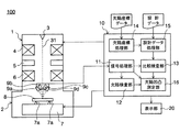
図1は、第1の実施形態に係る欠陥レビュー装置を示すブロック図であり、図2は、第1の実施形態に係る欠陥レビュー装置の電子検出器の配置を示す模式図である。
(First embodiment)
FIG. 1 is a block diagram illustrating a defect review apparatus according to the first embodiment, and FIG. 2 is a schematic diagram illustrating an arrangement of electron detectors of the defect review apparatus according to the first embodiment.
図1に示すように、本実施形態の欠陥レビュー装置100は、試料8を収容するチャンバー2と、試料8に電子線を照射する電子走査部1と、電子走査部1及びチャンバー2内のステージ7の制御並びに測定データの処理を行う制御部10とに大別される。
As shown in FIG. 1, the
電子走査部1は、電子銃3を備え、電子銃3からは電子ビーム31が放出される。この電子ビーム31はコンデンサレンズ4で集束され、偏向コイル5で位置決めされた後、対物レンズ6による焦点合わせを経て試料8の表面に照射される。
The
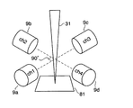
また、電子走査部1には、試料表面から放出される電子を検出するための4つの電子検出器9a〜9dが設けられている。
Further, the
図2に示すように、第1〜第4の電子検出器9a〜9dは、電子ビーム31の照射方向から見て、電子ビーム31の光軸の周りに相互に90°の角度を開けて対称に配置されている。ここでは、各電子検出器9a〜9dは矩形状の観察領域81の対角線方向に配置されるものとする。これらの電子検出器9a〜9dは、例えばシンチレータ等よりなり、試料8の上に電子ビーム31を照射することによって発生する二次電子や反射電子を捕捉して、各検出器の設置位置における電子量を、それぞれ信号ch1〜ch4として出力する。
As shown in FIG. 2, the first to
図1のように、チャンバー2には、支持体7aを上部に備えたステージ7が設けられている。このステージ7は支持体7aを介してウェハやフォトマスク等の試料8を保持するとともに、不図示の駆動機構により試料8を移動させることができる。
As shown in FIG. 1, the
制御部10は、試料8の表面の観察対象となる領域(観察領域)81(図2参照)を設定する欠陥座標処理部14と、観察領域81に対応する部分の設計データを抽出する設計データ処理部15とを備える。設計データは、試料であるフォトマスクやウェハのパターンの形状を表すデータであり、欠陥を含まないパターンの基準として、観察領域81のパターンの形状の判別や欠陥の検出等に用いられる。
The
さらに、制御部10は、電子検出器9a〜9dからの信号を処理して画像データ(SEM画像)を生成する信号処理部11と、信号処理部11で生成された画像データに基づいて欠陥の検出を行う欠陥検査部12及び比較検査部13と、欠陥の凹凸及び高さを測定する欠陥凹凸測定部16とを備える。
Further, the
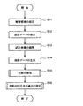
以下、欠陥レビュー装置100を用いた欠陥レビュー方法について説明する。図3は、欠陥レビュー装置100による欠陥レビュー方法を示すフローチャートである。
Hereinafter, a defect review method using the
まず、図3のステップS11のように、制御部10の欠陥座標処理部14が欠陥座標データに基づいて試料8の表面に矩形状の観察領域81を設定する。なお、欠陥座標データは、光学式の検査装置等で検出された欠陥の位置を表す座標データであり、通信回線などを通じて欠陥座標処理部14に入力される。
First, as in step S11 of FIG. 3, the defect coordinate processing
次のステップS12において、制御部10の設計データ処理部15が欠陥座標処理部14で設定された観察領域81の設計データを抽出し、これを記憶部(不図示)に記憶させる。
In the next step S12, the design
次に、ステップS13において、制御部10の制御の下で電子走査部1及びステージ7を駆動させて試料8の観察を行う。ここでは、制御部10がステージ7に制御信号を出力して、試料8の位置決めを行なう。その後、制御部10が電子走査部1に制御信号を出力して電子ビーム31を試料8の観察領域81内に照射して走査させる。このとき試料表面から放出される電子は電子検出器9a〜9dによって捕捉され、電子検出器9a〜9dは検出した電子の量を信号ch1〜ch4として信号処理部11に送出する。
Next, in step S <b> 13, the
次のステップS14において、制御部10の信号処理部11は、電子検出器9a〜9dから送出された信号ch1〜ch4をAD変換器でデジタル信号に変換し、このデジタル信号に基づいて画像データ(SEM画像)を生成する。
In the next step S14, the
図4は、信号処理部11が生成する画像データを示す模式図である。
FIG. 4 is a schematic diagram illustrating image data generated by the
図4に示すように、信号処理部11は、信号ch1〜ch4に基づいて左下画像a1、左上画像a2、右上画像a3及び右下画像a4を生成する。左下画像a1、左上画像a2、右上画像a3及び右下画像a4は、観察領域81をそれぞれ左下、左上、右上及び右下の各方向から写したSEM画像に相当する。
As illustrated in FIG. 4, the
また、信号処理部11は、隣接する電子検出器からの信号同士を加算することにより、各電子検出器9a〜9dの中間方向(左、右、下、及び上)から観察領域81を写したSEM画像に相当する、左画像a5、右画像a6、下画像a7及び上画像a8を生成する。
Moreover, the
さらに、信号処理部11は、ch1〜ch4を全て加算することにより、全加算画像a9を生成する。この全加算画像a9は、通常の走査型電子顕微鏡による二次電子像と同様な画像であり、全ての方向のエッジが略同一の高い輝度で表示されるため、欠陥の平面形状の測定等に用いられる。
Furthermore, the
信号処理部11で生成された画像a1〜a8は、それぞれ異なる向きのエッジ(斜面)が強調されて表示される。ここに、図5は試料8の表面の凸状のパターンの一例を示す図である。図5において、71は左下、左上、右上及び右下の各方向を向いたエッジ71a〜71dを有する凸状のパターンを示し、72は左、右、下及び上の各方向を向いたエッジ72a〜72dを有する凸状のパターンを示す。
The images a <b> 1 to a <b> 8 generated by the
図5のような試料を観察すると、左下画像a1では左下を向いたエッジ71aが最も高い輝度を示し、左上画像a2では左上を向いたエッジ71bが最も高い輝度を示す。また、右上画像a3及び右下画像a4では、それぞれエッジ71c、エッジ71dが最も高い輝度を示す。そして、左画像a5、右画像a6、下画像a7及び上画像a8では、それぞれエッジ72a、エッジ72b、エッジ72c及びエッジ72dが最も高い輝度を示す。
When the sample as shown in FIG. 5 is observed, the
以上のようにして、信号処理部11で生成された画像データは記憶部(不図示)に記憶される。
As described above, the image data generated by the
その後、図3のステップS15において、欠陥検査部12又は比較検査部13で欠陥の検出を行い、ステップS16において、欠陥凹凸測定部16が欠陥の凹凸及び高さの測定を行う。
Thereafter, in step S15 of FIG. 3, the
以下、ステップS15の欠陥の検出方法及びステップS16の欠陥の凹凸及び高さの測定方法について更に詳しく説明する。 Hereinafter, the defect detection method in step S15 and the defect unevenness and height measurement method in step S16 will be described in more detail.
図6は欠陥レビュー装置100による欠陥の検出方法を示すフローチャートである。図7は、欠陥レビュー装置100によるラインアンドスペースパターン上の欠陥検出の原理を説明する模式図である。図8は、ラインアンドスペースパターンの方向に応じた差分画像の生成方法を説明する模式図である。
FIG. 6 is a flowchart showing a defect detection method by the
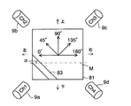
図6に示すように、先ずステップS21において、制御部10は、観察領域81の設計データを参照して、観察領域81のパターンが、縦、横、斜め45°及び斜め135°のラインアンドスペースパターンであるか否かを判断する。観察領域81のパターンが縦、横、斜め45°及び斜め135°のラインアンドスペースパターンである場合(YES)には、ステップS22に移行して欠陥検査部12による欠陥の検出を行う。
As shown in FIG. 6, first, in step S <b> 21, the
ステップS22では、欠陥検査部12がラインパターンの延在方向に平行であって、電子ビーム31の光軸を挟んで向かい合う2方向からの画像データを記憶部から取得し、これらの画像データの差分を取って差分画像を生成する。
In step S22, the
例えば、図7に示すように、観察領域81のパターンが横方向のラインアンドスペースパターンである場合には、欠陥検査部12は、左画像a5と、右画像a6を記憶部から取得してこれらの差分をとる。なお、図7において、符号99a、99bは、それぞれ左画像a5及び右画像a6に対応する仮想的な電子検出器の位置を示すものとする。
For example, as shown in FIG. 7, when the pattern of the
図示のように、ラインパターン83の縁にはエッジ83a、83b存在するが、これらのエッジ83a、83bの向き(法線方向)は、電子検出器99a及び電子検出器99bの間の方向を向いている。そのため、これらのエッジ83a、83bは、左画像a5及び右画像a6においてほぼ同じ輝度を示す。また、ラインパターン83の上面及びスペース82の向き(法線方向)は、電子検出器99a及び電子検出器99bの中間の方向であるため、これらの部分も左画像a5及び右画像a6において同じ輝度で表される。そのため、左画像a5及び右画像a6との差分を取ると、エッジ83a、83b、ラインパターン83、及びスペース82が相殺されてラインアンドスペースパターンが消去される。
As shown in the figure, edges 83a and 83b exist at the edge of the
一方、欠陥85には電子検出器99a側を向いたエッジ85aと、電子検出器99b側を向いたエッジ85bとが存在する。この場合、左画像a5ではエッジ85aの輝度がエッジ85bの輝度よりも高くなる。また、右画像a6ではエッジ85bの輝度がエッジ85aの輝度よりも高くなる。そのため、左画像a5と右画像a6との差分をとると、欠陥85のエッジ85a、85bが除去されずに残る。
On the other hand, the
したがって、左画像a5と右画像a6との差分を取ることにより、ラインアンドスペースパターンが消去され、欠陥85のみが現れた差分画像が得られる。
Therefore, by taking the difference between the left image a5 and the right image a6, the line and space pattern is erased, and a difference image in which only the
なお、図8(a)のようにラインアンドスペースパターンの向きが縦(0°)の場合には、下画像a7と上画像a8との差分を取れば、欠陥のみが残った差分画像が得られる。また、図8(b)のような斜め45°のラインアンドスペースパターンの場合は、左下画像a1と右上画像a3との差分をとれば良く、図8(c)のような斜め135°のラインアンドスペースパターンの場合は、左上画像a2と右下画像a4との差分をとればよい。 When the line and space pattern orientation is vertical (0 °) as shown in FIG. 8A, if a difference between the lower image a7 and the upper image a8 is taken, a difference image in which only defects remain is obtained. It is done. Further, in the case of an oblique 45 ° line-and-space pattern as shown in FIG. 8B, the difference between the lower left image a1 and the upper right image a3 may be taken, and an oblique 135 ° line as shown in FIG. 8C. In the case of an and space pattern, the difference between the upper left image a2 and the lower right image a4 may be taken.
その後、図6のステップS23において、欠陥検査部12は、ステップS22で求めた差分画像に基づいて欠陥を検出する。この場合、例えば差分画像からエッジを抽出する処理を行うことにより迅速に欠陥を検出できる。
Thereafter, in step S23 of FIG. 6, the
一方、ステップS21において、観察領域81のパターンが縦、横、斜め45°及び斜め135°のラインアンドスペースパターンではないと判断された場合(NO)には、ステップS24に移行して比較検査部13による欠陥の検出を行う。
On the other hand, if it is determined in step S21 that the pattern of the
ステップS24では、比較検査部13が斜め方向のエッジを強調したエッジ強調画像を生成する。ここでは、左下画像a1及び右上画像a3の差分を取ることで、左上と右下とを結ぶ対角線方向のエッジを強調した画像を生成する。また、左上画像a2及び右下画像a4の差分を取ることで、左下と右上とを結ぶ対角線方向のエッジを強調した画像を生成する。そして、左下画像a1及び右上画像a3の差分を取った画像と、左上画像a2及び右下画像a4の差分を取った画像とを加算することにより、斜め方向のエッジを強調したエッジ強調画像を生成する。
In step S24, the
次に、ステップS25において、比較検査部13は、ステップS24で生成したエッジ強調画像と、設計データとを重ね合わせ比較して、エッジ強調画像と設計データとのエッジ位置の相違部分に基づいて欠陥を検出する。このように、比較検査部13による検出処理により、所定方向のラインアンドスペースパターン以外の任意のパターンの欠陥を検出できる。
Next, in step S25, the
次に、上記の方法で検出した欠陥の凹凸及び高さ(又は深さ)の測定方法について説明する。図9は、欠陥の凹凸及び高さの測定の原理を説明する模式図である。 Next, a method for measuring the unevenness and height (or depth) of the defect detected by the above method will be described. FIG. 9 is a schematic diagram for explaining the principle of measurement of the unevenness and height of a defect.
一般に、凹凸を有する試料表面を電子ビーム31で走査したときに、電子検出器からの信号の強度は電子ビーム31が照射されている部分の試料表面の向きに応じて変化する。すなわち、電子ビーム31が照射されている部分の試料表面の向き(法線方向)が電子検出器の設置方向に近い程、電子検出器からの信号の強度が大きくなる。
In general, when an uneven sample surface is scanned with the
したがって、図9(a)のような断面を有する試料の表面に沿って電子ビーム31を走査させ、電子ビーム31を挟んで向かい合う2台の電子検出器99a、99bで試料表面から放出される電子を検出すると、電子検出器99aからは図9(b)の信号波形が得られ、電子検出器99bからは図9(c)の信号波形が得られる。
Therefore, the
図9(b)に示すように、電子検出器99aの信号波形は、電子検出器99a側を向いた凹凸87の左側の斜面で高くなり、電子検出器99aの設置方向から離れた方向を向いた凹凸87の右側の斜面で低くなる。すなわち、図9(b)の信号波形は、電子検出器99aの設置方向に対する試料表面の向き(法線方向)を反映している。
As shown in FIG. 9B, the signal waveform of the
また、図9(c)に示すように、電子検出器99bからの信号波形は、電子検出器99bの設置方向と離れた方向を向いた凹凸87の左側の斜面で低くなり、電子検出器99bの設置方向側を向いた凹凸87の右側の斜面で高くなる。すなわち、図9(c)の信号波形は、電子検出器99bの設置方向に対する試料表面の向き(法線方向)を反映している。
Further, as shown in FIG. 9C, the signal waveform from the
図9(b)、(c)の信号波形の差分をとると、図9(d)のような試料の表面の差分プロファイルが得られる。この差分プロファイルでは、試料表面の平坦部分からの信号が消去される。上記のように、図9(b)、(c)の信号波形は、それぞれ電子検出器99a及び電子検出器99bに対する凹凸87の表面の向きを反映しており、図9(b)、(c)の差分を取った差分プロファイルは試料表面の平坦部分に対する凹凸87の表面の傾斜の大きさを反映したものとなる。
When the difference between the signal waveforms in FIGS. 9B and 9C is taken, a difference profile on the surface of the sample as shown in FIG. 9D is obtained. In this differential profile, the signal from the flat part of the sample surface is erased. As described above, the signal waveforms in FIGS. 9B and 9C reflect the orientation of the surface of the
したがって、図9(d)の波形を積分することにより、図9(e)のように、試料表面の凹凸87の形状を反映した積分プロファイルが得られる。この凹凸87を反映した積分プロファイルが凹であるか凸であるかを調べることにより、凹凸87が試料表面から突出した凸状のものか、試料表面がえぐられた凹状のものかを判別することができる。
Therefore, by integrating the waveform of FIG. 9D, an integration profile reflecting the shape of the
また、予め高さが判明しているパターン(以下、参照パターンと呼ぶ)について、上記と同様の手順で積分プロファイルを求め、その参照パターンの積分プロファイルと凹凸87を反映した積分プロファイルとの高さを比較することにより、凹凸87の実際の高さを求めることができる。
Further, for a pattern whose height is known in advance (hereinafter referred to as a reference pattern), an integration profile is obtained by the same procedure as described above, and the height of the integration profile of the reference pattern and the integration profile reflecting the
そこで、本実施形態では、下記の方法により欠陥の高さを検出する。図10は、欠陥レビュー装置100による欠陥の凹凸及び高さの測定方法を示すフローチャートであり、図11は、同じく欠陥の凹凸及び高さの測定方法を説明する模式図である。なお、図11において、符号31は電子ビームを示し、符号83はラインパターンを示し、符号85は欠陥を示す。
Therefore, in the present embodiment, the height of the defect is detected by the following method. FIG. 10 is a flowchart showing a method for measuring the unevenness and height of the defect by the
まず、図10のステップS31のように、制御部10の欠陥凹凸測定部16が欠陥の差分プロファイルを取得する。例えば図11(a)に示すように、欠陥凹凸測定部16が電子ビーム31を挟んで向かい合う2方向からの画像データ(左画像a5及び右画像a6)を抽出する。そして、図11(b)に示すように、それらの画像データの差分を取ることにより差分画像b1を求める。次に、その差分画像b1において、左画像a5及び右画像a6の方向(左右方向)に平行で欠陥85を通るラインAを設定し、そのラインAに沿った部分の差分値を抽出する。これにより、図11(c)に示すように欠陥の差分プロファイルが求まる。
First, as in step S31 of FIG. 10, the defect
次に、図10のステップS32において、欠陥凹凸測定部16はステップS31で求めた差分プロファイルを積分して欠陥を反映した積分プロファイルを算出する。すなわち、図11(c)の差分プロファイルを積分してゆくことにより、図11(d)のように積分プロファイルを算出する。この積分プロファイルは、ラインAに沿った断面における欠陥の高さの分布を反映している。
Next, in step S32 of FIG. 10, the defect
次のステップS33において、欠陥凹凸測定部16は、欠陥を反映した積分プロファイルが上に凸であるか凹であるかを調べることにより、欠陥が試料表面から突出した凸状のものであるか、試料表面がえぐれて形成された凹状のものであるかを判別する。例えば、図11(a)の欠陥85は、図11(d)の積分プロファイルに基づいて、凸状であると判別される。
In the next step S33, the defect
次に、ステップS34で、欠陥凹凸測定部16は、参照パターンの差分プロファイルを求める。例えば図11(a)に示す試料において、高さが判明しているラインパターン83がある場合には、そのラインパターン83を参照パターンとする。この場合には、ラインパターン83と直交する方向の画像データ(下画像a7及び上画像a8)の差分を取った差分画像を生成する。そして、図11(a)のような、ラインパターン83と直交するラインBを設定し、そのラインBに沿った部分の差分値を差分画像から抽出して、参照パターンの差分プロファイルを求める。
Next, in step S34, the defect
次いで、ステップS35で、欠陥凹凸測定部16は、ステップS34で求めた参照パターンの差分プロファイルを積分して、参照パターンの積分プロファイル(図11(e)参照)を求める。
Next, in step S35, the defect
その後、ステップS36において、欠陥を反映した積分プロファイルのピーク値と、参照パターンの積分プロファイルのピーク値とを比較することにより、欠陥の高さHを算出する。例えば、図11(d)、(e)に示すように、欠陥を反映した積分プロファイルのピーク値がI1であり、参照パターンの積分プロファイルのピーク値がI2である場合には、欠陥及び参照パターンの積分プロファイルのピーク値の比がI1/I2と求まる。そして、図11(a)に示すように参照パターン(ラインパターン83)の実際の高さがH0である場合には、欠陥及び参照パターンの積分プロファイルの比I1/I2に参照パターンの高さH0を乗ずることにより、欠陥85の高さH(=I1/I2×H0)が求まる。
After that, in step S36, the height H of the defect is calculated by comparing the peak value of the integral profile reflecting the defect with the peak value of the integral profile of the reference pattern. For example, as shown in FIGS. 11D and 11E, when the peak value of the integral profile reflecting the defect is I1 and the peak value of the integral profile of the reference pattern is I2, the defect and the reference pattern The ratio of the peak values of the integration profile is obtained as I1 / I2. Then, when the actual height of the reference pattern (line pattern 83) is H0 as shown in FIG. 11A, the height H0 of the reference pattern is set to the ratio I1 / I2 of the integral profile of the defect and the reference pattern. Is multiplied by the height H (= I1 / I2 × H0) of the
以上のように、本実施形態によれば、観察領域81がラインアンドスペースパターンである場合には、差分画像に基づいて欠陥を迅速に検出できる。また、本実施形態によれば、試料の回転させることなく縦、横、斜め45°及び斜め135°の4方向のラインアンドスペースパターン上の欠陥を検出できるので、欠陥の検出処理がより一層迅速化される。
As described above, according to the present embodiment, when the
さらに、欠陥を反映した積分プロファイルに基づいて、欠陥が凹であるか又は凸であるかを判別できるとともに、参照パターンの積分プロファイルと比較することにより欠陥の高さを検出できる。 Furthermore, based on the integral profile reflecting the defect, it can be determined whether the defect is concave or convex, and the height of the defect can be detected by comparing with the integral profile of the reference pattern.
(実験例1)
実験例1の試料は、ガラス基板の上に厚さが約80nm及び幅が約80nmのクロム(Cr)からなる複数のラインパターンを形成したものであり、各ラインパターンの間には幅が約80nmのスペースが設けられている。ここでは、ラインパターンは観察領域81において横方向に伸びているものとする。
(Experimental example 1)
The sample of Experimental Example 1 is formed by forming a plurality of line patterns made of chromium (Cr) having a thickness of about 80 nm and a width of about 80 nm on a glass substrate, and the width is about between each line pattern. A space of 80 nm is provided. Here, it is assumed that the line pattern extends in the horizontal direction in the
図12(a)は実験例1の試料の右画像a6を示し、図12(b)は実験例1の試料の左画像a5を示し、図12(c)は実験例1の試料の全加算画像a9を示し、図12(d)は右画像a6と左画像a5との差分をとった差分画像を示す。 12A shows the right image a6 of the sample of Experimental Example 1, FIG. 12B shows the left image a5 of the sample of Experimental Example 1, and FIG. 12C shows the total addition of the sample of Experimental Example 1. An image a9 is shown, and FIG. 12D shows a difference image obtained by taking the difference between the right image a6 and the left image a5.
図12(a)〜(c)に示すように、観察領域81の中央部に矩形状のパターンが現れているが、従来であれば、この矩形状のパターンが欠陥であるか否かは設計データや正常なパターンの観察結果とのパターンマッチング(比較処理)を行うまで判別できない。
As shown in FIGS. 12A to 12C, a rectangular pattern appears in the central portion of the
しかし、本実験例では、図12(d)のように、左画像a5と右画像a6との差分を取ることにより、ラインアンドスペースパターンが消去され、欠陥のみが現れた差分画像が得られる。これにより、欠陥を容易に検出できることが分かる。 However, in this experimental example, as shown in FIG. 12D, by taking the difference between the left image a5 and the right image a6, the line and space pattern is erased and a difference image in which only the defect appears is obtained. Thereby, it turns out that a defect can be detected easily.
次に、検出した欠陥の差分プロファイル及び積分プロファイルを求めた結果を図13に示す。図13(a)は、図12(d)のI−I線における差分プロファイルを示すグラフであり、図13(b)は、図13(a)の差分プロファイルを積分して得た積分プロファイルを示すグラフである。 Next, FIG. 13 shows the results of obtaining the differential profile and integral profile of the detected defects. FIG. 13A is a graph showing the difference profile along the line II in FIG. 12D, and FIG. 13B shows the integration profile obtained by integrating the difference profile of FIG. It is a graph to show.
図13(b)のように、欠陥の積分プロファイルは上に凸状であることから、欠陥が凸状であることが分かる。また、欠陥の積分プロファイルのピーク値は約600(輝度値)であった。 As shown in FIG. 13B, since the integral profile of the defect is convex upward, it can be seen that the defect is convex. The peak value of the defect integration profile was about 600 (luminance value).
次に、参照パターンの積分プロファイルを算出し、欠陥の高さを求めた結果について説明する。図14は、実験例1の試料の差分画像、差分プロファイル及び積分プロファイルを示す図である。 Next, the result of calculating the integral profile of the reference pattern and obtaining the height of the defect will be described. FIG. 14 is a diagram illustrating a difference image, a difference profile, and an integration profile of the sample of Experimental Example 1.
図14(a)に示すように、実験例1では、ラインパターンを参照パターンとし、ラインパターンの延在方向と直交する方向に向かい合う上画像a8及び下画像a7の差分を取った差分画像を生成した。そして、その差分画像からラインパターンを横切るII−II線での差分値を抽出することにより、図14(b)に示す差分プロファイルを得た。また、図14(b)の差分プロファイルを積分することにより、図14(c)に示すような参照パターンの積分プロファイルを求めた。 As shown in FIG. 14A, in Experimental Example 1, a line pattern is used as a reference pattern, and a difference image is generated by taking the difference between the upper image a8 and the lower image a7 facing in the direction orthogonal to the extending direction of the line pattern. did. And the difference profile shown in FIG.14 (b) was obtained by extracting the difference value in the II-II line which crosses a line pattern from the difference image. Further, by integrating the difference profile of FIG. 14B, an integration profile of the reference pattern as shown in FIG. 14C was obtained.
図14(c)に示すように、参照パターンの積分プロファイルのピーク値は約1000(輝度値)であることが分かる。また、この参照パターンの(ラインパターン)の高さは80nmであることが分かっている。したがって、欠陥を反映した積分プロファイル及び参照パターンの積分プロファイルのピーク値の比は、600/1000であり、これに参照パターンの高さ80nmを乗ずることにより、欠陥の高さが約48nm(=600/1000×80nm)と求まる。 As shown in FIG. 14C, it can be seen that the peak value of the integration pattern of the reference pattern is about 1000 (luminance value). Further, it is known that the height of the reference pattern (line pattern) is 80 nm. Therefore, the ratio of the peak value of the integral profile reflecting the defect and the integral profile of the reference pattern is 600/1000. By multiplying this by the height of the reference pattern of 80 nm, the height of the defect is about 48 nm (= 600 / 1000 × 80 nm).
(実験例2)
実験例2では、凹状の欠陥を有する試料の欠陥レビューを行った例について説明する。
(Experimental example 2)
In Experimental Example 2, an example in which a defect review of a sample having a concave defect is performed will be described.
実験例2の試料は、実験例1と同様に、ガラス基板の上に高さが約80nm及び幅が約80nm及びのクロム(Cr)からなる複数のラインパターンを設けたものであり、各ラインパターンの間には幅が約80nmのスペースが設けられている。実験例2においても、ラインパターンは横方向に配置されているものとする。 Similar to Experimental Example 1, the sample of Experimental Example 2 is provided with a plurality of line patterns made of chromium (Cr) having a height of about 80 nm and a width of about 80 nm on a glass substrate. A space having a width of about 80 nm is provided between the patterns. Also in Experimental Example 2, the line patterns are arranged in the horizontal direction.
図15(a)は、実験例2の試料の全加算画像a9を示す図であり、図15(b)は、実験例2の試料の左画像a5と右画像a6との差分画像を示す図である。 FIG. 15A is a diagram showing a fully added image a9 of the sample of Experimental Example 2, and FIG. 15B is a diagram showing a difference image between the left image a5 and the right image a6 of the sample of Experimental Example 2. It is.
図15(a)に示すように、観察領域81の中央部に矩形状のパターンが確認できる。また、図15(b)の差分画像により、図15(a)の矩形状のパターンが欠陥であることが分かる。
As shown in FIG. 15A, a rectangular pattern can be confirmed at the center of the
次に、欠陥の差分プロファイル及び積分プロファイルを求めた結果を図16に示す。図16(a)は、図15(b)のIII−III線での差分プロファイルを示す図であり、図16(b)は、図16(a)の差分プロファイルを積分して得られる欠陥の積分プロファイルを示す図である。 Next, FIG. 16 shows the results of obtaining the defect difference profile and the integral profile. FIG. 16A is a diagram showing a differential profile along the line III-III in FIG. 15B, and FIG. 16B is a diagram showing defects obtained by integrating the differential profile in FIG. It is a figure which shows an integration profile.
図16(b)に示すように、欠陥の積分プロファイルは凹状であり、この欠陥は、ラインアンドスペースパターンの一部が削れてできた凹状のパターンであることが分かる。また、欠陥の積分プロファイルのピーク値は約−280(輝度値)であった。 As shown in FIG. 16B, it can be seen that the integral profile of the defect is concave, and this defect is a concave pattern formed by cutting a part of the line and space pattern. Further, the peak value of the defect integration profile was about −280 (luminance value).
次に、参照パターン(ラインパターン)の差分プロファイル及び積分プロファイルを求めた。図17(a)は、実験例2の試料の上画像a8及び下画像a7の差分をとった差分画像を示す図であり、図17(b)は図17(a)のIV−IV線における差分プロファイルを示す図であり、図17(c)は図17(b)の差分プロファイルを積分して得られる参照パターンの積分プロファイルを示す図である。 Next, a difference profile and an integration profile of the reference pattern (line pattern) were obtained. FIG. 17A is a diagram showing a difference image obtained by taking the difference between the upper image a8 and the lower image a7 of the sample of Experimental Example 2, and FIG. 17B is a line IV-IV in FIG. FIG. 17C is a diagram showing an integration profile of a reference pattern obtained by integrating the difference profile of FIG. 17B.
図17(c)に示すように、参照パターンの積分プロファイルのピーク値は約560(輝度値)であった。また、参照パターンの高さは80nmであることが分かっている。したがって、欠陥及び参照パターンの積分プロファイルのピーク値の比は−280/560であり、これに参照パターンの高さ(80nm)を乗ずることにより、図15(a)の欠陥の高さ(深さ)が約−40nm(=−280/560×80nm)と求まる。 As shown in FIG. 17C, the peak value of the integration profile of the reference pattern was about 560 (luminance value). Further, it is known that the height of the reference pattern is 80 nm. Therefore, the ratio of the peak value of the integral profile of the defect and the reference pattern is −280/560, and by multiplying this by the height of the reference pattern (80 nm), the height (depth) of the defect in FIG. ) Is found to be about −40 nm (= −280 / 560 × 80 nm).
(第1の実施形態の変形例)
上記の欠陥レビュー装置100では電子検出器を4台設けているが、これに限定されるものではなく、電子検出器9は少なくとも2台以上の任意の台数とすることができる。
(Modification of the first embodiment)
In the
図18は、第1の実施形態の変形例に係る欠陥レビュー装置100の電子検出器の配置を示す模式図であり、電子検出器を3台とした場合の配置を示している。
FIG. 18 is a schematic diagram showing the arrangement of the electron detectors of the
図18に示すように、電子検出器を3台とする場合には、第1〜第3の電子検出器9a〜9cは電子ビーム31の照射方向から見て電子ビーム31の光軸の周りに相互に120°の角度を開けて配置する。
As shown in FIG. 18, when the number of electron detectors is three, the first to
また、信号処理部11は、各電子検出器9a〜9cからの信号ch1〜ch3に基づいて、各電子検出器9a〜9cの設置方向から観察領域を写した第1の画像c1、第2の画像c2及び第3の画像c3を生成する。さらに信号処理部11は、隣接する電子検出器からの信号同士を加算して第4の画像c4、第5の画像c5及び第6の画像c6を生成するとともに、ch1〜ch3を加算して全加算画像c7を生成する。なお、第4〜第6の画像c4、c5、c6は、各電子検出器9a、9b、9cの中間の方向から観察領域を写したSEM画像に相当する。
The
図19は、図18に示す変形例における差分画像の生成方法を説明する模式図である。 FIG. 19 is a schematic diagram illustrating a method of generating a difference image in the modification example illustrated in FIG.
本変形例では、60°及び120°のラインアンドスペースパターンである場合に、欠陥検査部12による欠陥の検出を行なう。
In this modification, the
この場合、図19(a)のように、縦方向(0°)のラインアンドスペースパターンに対しては、第4の画像c4と第1の画像c1との差分をとってラインアンドスペースパターンが消去された差分画像を生成し、その差分画像に基づいて欠陥を検出する。また、図19(b)のように、60°方向のラインアンドスペースパターンに対しては、第6の画像c6と第3の画像c3との差分をとった差分画像に基づいて欠陥を検出する。さらに、図19(c)のように、120°方向のラインアンドスペースパターンの場合には、第5の画像c5と第2の画像c2との差分を取った差分画像に基づいて欠陥を検出する。 In this case, as shown in FIG. 19A, for the line and space pattern in the vertical direction (0 °), the line and space pattern is obtained by calculating the difference between the fourth image c4 and the first image c1. An erased difference image is generated, and a defect is detected based on the difference image. Further, as shown in FIG. 19B, a defect is detected based on a difference image obtained by taking the difference between the sixth image c6 and the third image c3 with respect to the 60 ° direction line and space pattern. . Further, as shown in FIG. 19C, in the case of a 120 ° direction line and space pattern, a defect is detected based on a difference image obtained by taking a difference between the fifth image c5 and the second image c2. .
なお、本変形例の欠陥検査装置100において、電子検出器を2台としてもよい。この場合には、電子検出器を電子ビーム31の光軸を挟んで対向するように配置すればよく、ステージ7に回転機構を設けて任意の方向のラインアンドスペースパターン上の欠陥を検出できるようにしてもよい。
In addition, in the
(第2の実施形態)
第2の実施形態では、任意の方向のラインパターンについて差分画像に基づいて欠陥を検出する方法について説明する。なお、本実施形態でも、図1に示す欠陥レビュー装置100により欠陥の検出を行う。
(Second Embodiment)
In the second embodiment, a method for detecting a defect based on a difference image for a line pattern in an arbitrary direction will be described. Also in this embodiment, the defect is detected by the
図20は本実施形態における欠陥レビュー方法を示すフローチャートである。 FIG. 20 is a flowchart showing a defect review method according to this embodiment.
図20に示すように、欠陥レビュー装置100は、ステップS41において観察領域81を設定する。その後、ステップS42に移行して、観察領域81の設計データを抽出する。さらに、ステップS43において観察領域81に電子ビーム31を照射しつつ走査させて試料表面の観察を行う。なお、上記のステップS41〜S43は図3を参照しつつ説明したステップS11〜S13と同様である。
As shown in FIG. 20, the
次に、ステップS44において欠陥レビュー装置100の信号処理部11は各電子検出器9a〜9dからの検出信号ch1〜ch4に基づいて観察領域81を複数の方向から写した画像を生成する。
Next, in step S44, the
図21は、ステップS44における画像の生成方法を示すフローチャートである。 FIG. 21 is a flowchart showing an image generation method in step S44.
まず、図21のステップS51において、信号処理部11は各電子検出器9a〜9dからの検出信号ch1〜ch4に基づいて、左下画像a1、左上画像a2、右上画像a3及び右下画像a4を生成する。これらの画像は、観察領域81をそれぞれ、左下、左上、右上及び右下の各方向から写したSEM画像に相当する。
First, in step S51 of FIG. 21, the
次に、ステップS52において、信号処理部11は、設計データを参照して、観察領域81上のパターンがラインアンドスペースパターンか否かを判断する。ステップS52において、信号処理部11が観察領域81上のパターンがラインアンドスペースパターンであると判断した場合(YES)にはステップS53に移行し、ラインアンドスペースパターンでないと判断した場合(NO)には画像の生成を終了する。
Next, in step S52, the
次に、ステップS53において、信号処理部11は、設計データに基づいて、ラインアンドスペースパターンに含まれるラインパターンの角度αを検出する。
Next, in step S53, the
ここで、図22は、本実施形態におけるラインパターンの角度αの定義を示す図である。 Here, FIG. 22 is a diagram showing the definition of the angle α of the line pattern in the present embodiment.
本実施形態では、図22のように左右方向に延在する直線Mと、ラインパターン83の延在方向とのなす角度をラインパターンの角度αとする。また、180°以上の角度のラインパターンは、その角度から180°を差し引いた角度のラインパターンと同じものとして扱う。たとえば、200°のラインパターンは20°のラインパターンとして扱うものとする。
In the present embodiment, the angle formed by the straight line M extending in the left-right direction and the extending direction of the
次に、ステップS54に移行して、信号処理部11は、ラインパターンの角度αが45°〜135°であるか否かを判断する。ステップS54において信号処理部11がラインパターンの角度αが45°〜135°であると判断した場合(YES)には、ステップS55に移行する。
Next, proceeding to step S54, the
図23(a)は、本実施形態において、ラインパターンの角度αが45°〜135°の場合の左画像、右画像、上画像及び下画像の生成方法を説明する模式図である。また、図24(a)〜(d)は、本実施形態での左画像、右画像、上画像及び下画像の生成に用いる係数r1〜r4をそれぞれ示す図である。 FIG. 23A is a schematic diagram illustrating a method for generating a left image, a right image, an upper image, and a lower image when the line pattern angle α is 45 ° to 135 ° in the present embodiment. FIGS. 24A to 24D are diagrams showing coefficients r1 to r4 used for generating the left image, the right image, the upper image, and the lower image in the present embodiment, respectively.
ステップS55では、信号処理部11は、図23(a)に示すように左画像d1を、係数r1を乗じた信号ch1と係数r2を乗じた信号ch2とを加算して生成する。また、右画像d2を、係数r3を乗じた信号ch3と係数r4を乗じた信号ch4とを加算して生成する。
In step S55, the
さらに、信号処理部11は、上画像d3を、係数r3を乗じた信号ch2と係数r2を乗じた信号ch3とを加算して生成し、下画像d4を、係数r4を乗じた信号ch1と係数r1を乗じた信号ch4とを加算して生成する。
Further, the
上記各画像d1〜d4の生成に用いる係数r1〜r4は、図24(a)〜(d)にそれぞれ示すように、ラインパターンの角度αに応じて0〜1の間で周期的に変化する。ここでは、係数r1、r3は(1+sin2α)/2で表され、係数r2、r4は(1−sin2α)/2で表わされるものとする。 The coefficients r1 to r4 used for generating the images d1 to d4 change periodically between 0 and 1 according to the line pattern angle α, as shown in FIGS. . Here, the coefficients r1 and r3 are represented by (1 + sin2α) / 2, and the coefficients r2 and r4 are represented by (1−sin2α) / 2.
上画像d3の生成に用いる係数r2、r3に着目すると、図24(b)、(c)に示すように、ラインパターンの角度αが、信号ch3に対応する電子検出器9cの設置方向である135°に近づくほど、信号ch3に係る係数r2が増大し、信号ch2に係る係数r3が減少する。これとは逆に、ラインパターンの角度αが信号ch2に対応する電子検出器9bの設置方向である45°に近づくと、信号ch2に係る係数r3が増大し、信号ch3に係る係数r2が減少する。このようにして、ラインパターンの角度αが電子検出器9cの設置方向に近づくと、上画像d3において電子検出器9cからの信号ch3の割合が増加する。また、ラインパターンの角度αが電子検出器9bの設置方向に近づくと上画像d3において電子検出器9bからの信号ch2の割合が増加する。
Focusing on the coefficients r2 and r3 used to generate the upper image d3, as shown in FIGS. 24B and 24C, the angle α of the line pattern is the installation direction of the
そして、上画像d3が観察領域を写す方向は、角度αが45°〜135°のラインパターンに対してラインパターンの延在方向に平行な方向となる。 The direction in which the upper image d3 captures the observation region is a direction parallel to the extending direction of the line pattern with respect to the line pattern having the angle α of 45 ° to 135 °.
同様に、下画像d4はラインパターンの延在方向に平行な方向から写した画像となる。 Similarly, the lower image d4 is an image copied from a direction parallel to the extending direction of the line pattern.
一方、左画像d1及び右画像d2は、ラインパターンの延在方向に直交する方向から写した画像となる。 On the other hand, the left image d1 and the right image d2 are images taken from a direction orthogonal to the extending direction of the line pattern.
以上のように、ステップS55において信号処理部11は、ラインパターンの延在方向に平行な方向から写した上画像d3及び下画像d4と、ラインパターンの延在方向に直交する方向から写した左画像d1及び右画像d2とを生成する。
As described above, in step S55, the
図21のステップS54において、信号処理部11がラインパターンの角度αが45°〜135°でないと判断した場合(NO)、すなわちラインパターンの角度αが0°〜45°又は135°〜180°の場合は、ステップS56に移行する。
In step S54 of FIG. 21, when the
図23(b)は、ラインパターンの角度αが0°〜45°または135°〜180°の場合における左画像、右画像、上画像及び下画像の生成方法を説明する模式図である。 FIG. 23B is a schematic diagram illustrating a method for generating a left image, a right image, an upper image, and a lower image when the line pattern angle α is 0 ° to 45 ° or 135 ° to 180 °.
ステップS56において、信号処理部11は図23(b)に示すように左画像d1を、係数r2を乗じた信号ch1と係数r1を乗じた信号ch2とを加算して生成する。また、右画像d2を、係数r4を乗じた信号ch3と係数r3を乗じた信号ch4とを加算して生成する。
In step S56, the
さらに、信号処理部11は、上画像d3を、係数r2を乗じた信号ch2と係数r3を乗じた信号ch3とを加算して生成し、下画像d4を、係数r1を乗じた信号ch1と係数r4を乗じた信号ch4とを加算して生成する。
Further, the
ここでは、左画像d1及び右画像d2がラインパターンの延在方向に平行な方向から写した画像となり、上画像d3及び下画像d4はラインパターンの延在方向に直交する方向から写した画像となる。 Here, the left image d1 and the right image d2 are images taken from a direction parallel to the extending direction of the line pattern, and the upper image d3 and the lower image d4 are images taken from a direction orthogonal to the extending direction of the line pattern. Become.
このようにして、ステップS56において信号処理部11は、ラインパターンの延在方向に平行な方向から写した左画像d1及び右画像d2と、ラインパターンの延在方向に直交する方向から写した上画像d3及び下画像d4とを生成する。
In this manner, in step S56, the
以上により、信号処理部11による画像の生成(ステップS44、図20)が完了する。
Thus, the image generation (step S44, FIG. 20) by the
次に、図20のステップS45に移行して、欠陥検査部12及び比較検査部13により欠陥の検出を行う。
Next, the process proceeds to step S45 in FIG. 20, and the
図25は、ステップS45における欠陥の検出方法を示すフローチャートである。 FIG. 25 is a flowchart showing the defect detection method in step S45.
まず、図25のステップS61において、欠陥検査部12は観察領域81のパターンがラインアンドスペースパターンか否かを判断する。ステップS61において、欠陥検査部12が観察領域81のパターンがラインアンドスペースパターンであると判断した場合(YES)には、ステップS62に移行する。
First, in step S61 in FIG. 25, the
次に、ステップS62において、欠陥検査部12は、ラインアンドスペースパターンを構成するラインパターンの延在方向に平行であって、電子ビーム31の光軸を挟んで向かい合う2方向からの画像データの差分をとって差分画像を生成する。
Next, in step S62, the
ここでは、ラインパターンの角度αが0°<α<45°又は135°<α<180°の場合には、左画像d1と右画像d2との差をとって差分画像を生成する。 Here, when the angle α of the line pattern is 0 ° <α <45 ° or 135 ° <α <180 °, a difference image is generated by taking the difference between the left image d1 and the right image d2.
また、ラインパターンの角度αが45°<α<135°の場合には、上画像d3と下画像d4との差をとって差分画像を生成する。 When the line pattern angle α is 45 ° <α <135 °, a difference image is generated by taking the difference between the upper image d3 and the lower image d4.
さらに、ラインパターンの角度αが45°の場合には、左上画像a2と右下画像a4との差をとって差分画像を生成する。また、ラインパターンの角度αが135°の場合には左下画像a1と右上画像a3との差をとって差分画像を生成する。 Further, when the line pattern angle α is 45 °, a difference image is generated by taking the difference between the upper left image a2 and the lower right image a4. When the line pattern angle α is 135 °, a difference image is generated by taking the difference between the lower left image a1 and the upper right image a3.
これにより、図7を参照しつつ説明したように、ラインパターンのエッジが消去されて欠陥85のみが残った差分画像が得られる。
As a result, as described with reference to FIG. 7, a difference image in which the edge of the line pattern is erased and only the
次に、図25のステップS63において、欠陥検査部12は、ステップS62で生成した差分画像に残ったパターンを欠陥として検出する。この場合、例えば差分画像において、所定の輝度値以上のエッジを検出することにより、欠陥のみを迅速に検出できる。
Next, in step S63 of FIG. 25, the
一方、ステップS61で、欠陥検査部12が観察領域81のパターンがラインアンドスペースパターンでないと判断した場合(NO)には、ステップS64に移行して比較検査部13によりエッジ強調画像を生成する。
On the other hand, if the
その後、ステップS65において、比較検査部13がエッジ強調画像と設計データとを重ね合わせて比較して、エッジ強調画像のエッジが設計データのエッジと異なる部分を欠陥として検出する。
Thereafter, in step S65, the
以上により、欠陥の検出が完了する。 Thus, the defect detection is completed.
その後、図20のステップS46に移行して、欠陥凹凸測定部16が欠陥の凹凸及び高さの測定を行う。なお、本実施形態の欠陥凹凸測定部16による欠陥の凹凸及び高さの測定は図9〜図11を参照しつつ説明した方法で行う。この場合、参照パターンの積分プロファイルは、ラインパターンの延在方向に直交する2方向からの画像に基づいて求めればよい。
Thereafter, the process proceeds to step S46 in FIG. 20, and the defect
以上のように、本実施形態によれば、隣接する信号同士にラインパターンの角度αに応じて変化する係数を乗じた上で加算することにより、任意の角度のラインパターンに対して、ラインパターンの延在方向に平行な方向から写した画像を生成する。これにより、任意の角度のラインパターンに対して、差分画像に基づいて迅速に欠陥を検出できる。 As described above, according to the present embodiment, by multiplying adjacent signals by a coefficient that changes according to the angle α of the line pattern, and adding them, a line pattern can be obtained with respect to a line pattern at an arbitrary angle. An image taken from a direction parallel to the extending direction is generated. Thereby, it is possible to quickly detect a defect based on the difference image with respect to a line pattern at an arbitrary angle.
(実験例3)
実験例3の試料は、ガラス基板の上に厚さが約80nm及び幅が約400nmのクロム(Cr)からなる複数のラインパターンを形成したものであり、各ラインパターンの間には、幅が約400nmのスペースが設けられている。本実験例において、ラインパターンの角度は105°とした。
(Experimental example 3)
In the sample of Experimental Example 3, a plurality of line patterns made of chromium (Cr) having a thickness of about 80 nm and a width of about 400 nm are formed on a glass substrate, and the width is between each line pattern. A space of about 400 nm is provided. In this experimental example, the angle of the line pattern was 105 °.
図26(a)は、実験例3の試料の左下画像a1を示し、図26(b)は実験例3の試料の左上画像a2を示し、図26(c)は実験例3の試料の右上画像a3を示し、図26(d)は実験例3の試料に右下画像a4を示す。 26A shows a lower left image a1 of the sample of Experimental Example 3, FIG. 26B shows an upper left image a2 of the sample of Experimental Example 3, and FIG. An image a3 is shown, and FIG. 26D shows a lower right image a4 on the sample of Experimental Example 3.
次に、係数r1、r3を0.25とし、係数r2、r4を0.75として、図23(a)に示す方法で左画像d1、右画像d2、上画像d3及び下画像d4を生成した。続いて、生成した各画像d1〜d4から図26(a)のVI−VI線に対応する部分の輝度の分布を抽出した。 Next, the coefficients r1, r3 are set to 0.25, the coefficients r2, r4 are set to 0.75, and the left image d1, the right image d2, the upper image d3, and the lower image d4 are generated by the method shown in FIG. . Subsequently, the luminance distribution of the portion corresponding to the VI-VI line in FIG. 26A was extracted from the generated images d1 to d4.
図27(a)は、左画像d1における輝度の分布を示し、図27(b)は右画像d2における輝度の分布を示す。また、図27(c)は上画像d3における輝度の分布を示し、図27(d)は下画像d4における輝度の分布を示す。 FIG. 27A shows the luminance distribution in the left image d1, and FIG. 27B shows the luminance distribution in the right image d2. FIG. 27C shows the luminance distribution in the upper image d3, and FIG. 27D shows the luminance distribution in the lower image d4.
次に、図27(a)の輝度の分布と図27(b)の輝度の分布との差分をとることにより、左画像d1及び右画像d2の差分プロファイルを求めた。また、図27(c)の輝度の分布と図27(d)の輝度の分布との差分をとることにより、上画像d3及び下画像d4の差分プロファイルを求めた。 Next, a difference profile between the left image d1 and the right image d2 was obtained by taking the difference between the luminance distribution in FIG. 27A and the luminance distribution in FIG. 27B. Also, the difference profile between the upper image d3 and the lower image d4 was obtained by taking the difference between the luminance distribution of FIG. 27C and the luminance distribution of FIG. 27D.
図28(a)は、左画像d1及び右画像d2の差分プロファイルを示し、図28(b)は上画像d3及び下画像d4の差分プロファイルを示す。 FIG. 28A shows a difference profile between the left image d1 and the right image d2, and FIG. 28B shows a difference profile between the upper image d3 and the lower image d4.
図28(a)に示すように、ラインパターンの延在方向に直交する方向から写した左画像d1及び右画像d2の差分プロファイルでは、ラインパターンのエッジが強調されて、エッジ部分に比較的大きな差分値の凸部及び凹部が表れている。 As shown in FIG. 28A, in the difference profile between the left image d1 and the right image d2 taken from the direction orthogonal to the extending direction of the line pattern, the edge of the line pattern is emphasized, and the edge portion is relatively large. The convex part and the concave part of the difference value appear.
これに対し、図28(b)に示すように、ラインパターンの延在方向に平行な方向から写した上画像d3及び下画像4の差分プロファイルでは、ラインパターンのエッジ部分の差分値の凹凸が図28(a)よりも小さくなり、ラインパターンのエッジがほぼ消去される。
On the other hand, as shown in FIG. 28B, in the difference profile of the upper image d3 and the
以上の結果から、ラインパターンの角度αが105°の場合でも、差分画像でラインパターンを消去できることが確認できた。 From the above results, it was confirmed that even when the line pattern angle α is 105 °, the line pattern can be erased from the difference image.
次に、ラインパターンの延在方向に直交する方向から写した左画像d1及び右画像d2の差分プロファイルを積分して積分プロファイルを求めた。図29は、図28(a)の差分プロファイルを積分して求めた積分プロファイルを示している。 Next, an integral profile was obtained by integrating the difference profiles of the left image d1 and the right image d2 taken from the direction orthogonal to the extending direction of the line pattern. FIG. 29 shows an integration profile obtained by integrating the difference profile of FIG.
図29に示すように、ラインパターンの延在方向に直交する方向から写した左画像d1及び右画像d2の積分プロファイルでは、ラインパターンの形状を反映して上に凸のピークが現れる。この積分プロファイルは参照パターンの積分プロファイルとして、欠陥の高さの測定に使用できる。 As shown in FIG. 29, in the integral profile of the left image d1 and the right image d2 taken from the direction orthogonal to the extending direction of the line pattern, a convex peak appears reflecting the shape of the line pattern. This integration profile can be used to measure the height of the defect as an integration profile of the reference pattern.
1…電子走査部、2…チャンバー、3…電子銃、4…コンデンサレンズ、5…偏向コイル、6…対物レンズ、7…ステージ、7a…保持部材、8…試料、9a〜9d…電子検出器、10…制御装置、11…信号処理部、12…欠陥検査部、13…比較検査部、14…欠陥座標処理部、15…設計データ処理部、16…欠陥凹凸測定部、17…記憶部、20…表示部、31…電子ビーム、81…観察領域、82…スペース、83…ラインパターン、83a、83b、85a、85b…エッジ、85…欠陥、87…凹凸。
DESCRIPTION OF
Claims (14)
前記電子ビームの光軸の周りに配置され、前記電子ビームの照射によって前記試料の表面から放出される電子を検出する複数の電子検出器と、
前記電子検出器の検出信号に基づいて、前記観察領域をそれぞれ異なる方向から写した複数の画像データを生成する信号処理部と、
前記複数の画像データの各々の差分をとった差分画像を生成し、該差分画像に基づいて前記観察領域内の欠陥を検出する欠陥検査部と、
を備え、
前記欠陥検査部は、前記観察領域のパターンがラインパターンとスペースとからなるラインアンドスペースパターンである場合には、前記ラインパターンの延在方向に平行で且つ前記電子ビームの光軸を挟んで対向する2方向からの前記画像データの差分を取って前記差分画像を生成し、該差分画像に残ったパターンを欠陥として検出することを特徴とする欠陥レビュー装置。 An electron scanning unit that irradiates the observation region of the sample surface with the electron beam and scans the electron beam within the observation region;
A plurality of electron detectors arranged around the optical axis of the electron beam and detecting electrons emitted from the surface of the sample by irradiation of the electron beam;
Based on the detection signal of the electron detector, a signal processing unit that generates a plurality of image data obtained by copying the observation region from different directions, and
A defect inspection unit that generates a difference image obtained by taking a difference between each of the plurality of image data, and detects a defect in the observation region based on the difference image;
Equipped with a,
When the pattern of the observation region is a line-and-space pattern made up of a line pattern and a space, the defect inspection unit is parallel to the extending direction of the line pattern and faces across the optical axis of the electron beam to take the differences of the image data from two directions to generate the difference image, defect review apparatus characterized that you detect the remaining pattern to said difference image as a defect.
前記欠陥凹凸測定部は、前記電子ビームの光軸を挟んで対向する2方向からの画像データの差分値の分布を示す差分プロファイルを求め、さらに前記差分プロファイルを積分して前記積分プロファイルを求め、前記欠陥を反映して前記積分プロファイルに現れる形が凹であるか凸であるかに基づいて、前記欠陥が凹であるか凸であるかを判別することを特徴とする請求項1乃至6のいずれか1項に記載の欠陥レビュー装置。 A defect unevenness measuring unit for measuring the unevenness of the defect,
The defect unevenness measuring unit obtains a difference profile indicating a distribution of difference values of image data from two directions facing each other across the optical axis of the electron beam, further integrates the difference profile to obtain the integral profile, based on whether the shape appearing in the integral profile to reflect the defect is a convex or a concave of claims 1 to 6 wherein the defect is characterized by determining whether a convex or a concave The defect review apparatus of any one of Claims.
前記電子検出器からの検出信号に基づいて、前記観察領域をそれぞれ異なる方向から写した複数の画像データを生成するステップと、
前記複数の画像データの各々の差分をとった差分画像を生成し、該差分画像に基づいて前記観察領域内の欠陥を検出するステップと、
を有し、
前記欠陥を検出するステップは、
前記観察領域のパターンがラインパターンとスペースとからなるラインアンドスペースパターンである場合には、前記ラインパターンの延在方向に平行で且つ前記電子ビームの光軸を挟んで対向する2方向からの前記画像データの差分を取って前記差分画像を生成するステップと、
前記差分画像に残ったパターンを欠陥として検出するステップと、
を有することを特徴とする欠陥レビュー方法。 Causes scanning while irradiating an electron beam to the observation area of the surface of the sample, the electron beam a plurality of electron detector the electrons emitted from the sample surface disposed about an optical axis of the electron beam by the irradiation of Detecting in step,
Generating a plurality of image data obtained by copying the observation region from different directions based on detection signals from the electron detector;
Generating a difference image obtained by taking a difference between each of the plurality of image data, and detecting a defect in the observation region based on the difference image;
Have
Detecting the defect comprises:
When the pattern of the observation region is a line-and-space pattern composed of a line pattern and a space, the direction from the two directions parallel to the extending direction of the line pattern and facing each other across the optical axis of the electron beam Taking the difference of the image data and generating the difference image;
Detecting a pattern remaining in the difference image as a defect;
A defect review method characterized by comprising:
前記凹凸を測定するステップは、
前記電子ビームの光軸を挟んで対向する2方向からの画像データの差分値の分布を示す差分プロファイルを求めるステップと、
前記差分プロファイルを積分して前記積分プロファイルを求めるステップと、
前記欠陥を反映して前記積分プロファイルに現れる形が凹であるか凸であるかに基づいて、前記欠陥が凹であるか凸であるかを判別するステップと、
を有することを特徴とする請求項10乃至11のいずれか1項に記載の欠陥レビュー方法。 Further comprising measuring irregularities of the detected defect,
The step of measuring the unevenness includes:
Obtaining a difference profile indicating a distribution of difference values of image data from two opposite directions across the optical axis of the electron beam;
Integrating the difference profile to determine the integral profile;
Determining whether the defect is concave or convex based on whether the shape appearing in the integral profile reflecting the defect is concave or convex; and
Defect review process according to any one of claims 10 to 11, wherein a.
高さが既知の参照パターンについて前記積分プロファイルを求めるステップと、
前記参照パターンについての前記積分プロファイルのピーク値と、前記欠陥を反映した前記積分プロファイルのピーク値とを比較することにより、前記欠陥の高さを算出するステップと、
を有することを特徴とする請求項12に記載の欠陥レビュー方法。 The step of measuring the unevenness of the defect comprises
Determining the integration profile for a reference pattern of known height;
Calculating the height of the defect by comparing the peak value of the integral profile for the reference pattern with the peak value of the integral profile reflecting the defect;
The defect review method according to claim 12 , further comprising:
隣り合う前記電子検出器の検出信号に前記ラインパターンの角度に応じて変化する係数を乗じて加算することにより前記ラインパターンの延在方向に平行で、且つ前記電子ビームの光軸を挟んで対向する2方向から前記観察領域を写した画像データを生成することを特徴とする請求項10乃至13のいずれか1項に記載の欠陥レビュー方法。 In the step of generating the image data,
Multiply the detection signals of the adjacent electron detectors by a coefficient that changes according to the angle of the line pattern, and add them in parallel to the direction in which the line pattern extends, and face each other across the optical axis of the electron beam The defect review method according to any one of claims 10 to 13 , wherein image data in which the observation area is copied from two directions is generated.
Priority Applications (5)
| Application Number | Priority Date | Filing Date | Title |
|---|---|---|---|
| JP2011087197A JP5548159B2 (en) | 2010-11-05 | 2011-04-11 | Defect review apparatus and defect review method |
| TW100136351A TW201220416A (en) | 2010-11-05 | 2011-10-06 | Defect review apparatus and defect review method |
| US13/317,317 US8779359B2 (en) | 2010-11-05 | 2011-10-14 | Defect review apparatus and defect review method |
| DE102011054537A DE102011054537A1 (en) | 2010-11-05 | 2011-10-17 | Apparatus for detecting defect in sample e.g. wafer for semiconductor component, produces subtraction image based on difference between image data of observation region in different directions to detect defect in observation region |
| KR1020110112581A KR20120048490A (en) | 2010-11-05 | 2011-10-31 | Defect review apparatus and defect review method |
Applications Claiming Priority (3)
| Application Number | Priority Date | Filing Date | Title |
|---|---|---|---|
| JP2010248446 | 2010-11-05 | ||
| JP2010248446 | 2010-11-05 | ||
| JP2011087197A JP5548159B2 (en) | 2010-11-05 | 2011-04-11 | Defect review apparatus and defect review method |
Publications (2)
| Publication Number | Publication Date |
|---|---|
| JP2012112927A JP2012112927A (en) | 2012-06-14 |
| JP5548159B2 true JP5548159B2 (en) | 2014-07-16 |
Family
ID=45443678
Family Applications (1)
| Application Number | Title | Priority Date | Filing Date |
|---|---|---|---|
| JP2011087197A Active JP5548159B2 (en) | 2010-11-05 | 2011-04-11 | Defect review apparatus and defect review method |
Country Status (5)
| Country | Link |
|---|---|
| US (1) | US8779359B2 (en) |
| JP (1) | JP5548159B2 (en) |
| KR (1) | KR20120048490A (en) |
| DE (1) | DE102011054537A1 (en) |
| TW (1) | TW201220416A (en) |
Families Citing this family (19)
| Publication number | Priority date | Publication date | Assignee | Title |
|---|---|---|---|---|
| JP5530959B2 (en) * | 2011-02-28 | 2014-06-25 | 株式会社アドバンテスト | Pattern height measuring device and pattern height measuring method |
| JP5530980B2 (en) * | 2011-06-14 | 2014-06-25 | 株式会社アドバンテスト | Pattern measuring apparatus and pattern measuring method |
| JP5438741B2 (en) * | 2011-10-26 | 2014-03-12 | 株式会社アドバンテスト | Pattern measuring apparatus and pattern measuring method |
| JP5787746B2 (en) * | 2011-12-26 | 2015-09-30 | 株式会社東芝 | Signal processing method and signal processing apparatus |
| JP6002470B2 (en) * | 2012-06-28 | 2016-10-05 | 株式会社日立ハイテクノロジーズ | Charged particle beam equipment |
| JP6084888B2 (en) | 2013-04-17 | 2017-02-22 | 株式会社アドバンテスト | Defect inspection apparatus and defect inspection method |
| JP6088337B2 (en) * | 2013-04-17 | 2017-03-01 | 株式会社アドバンテスト | Pattern inspection method and pattern inspection apparatus |
| KR101709433B1 (en) * | 2013-04-22 | 2017-02-22 | 가부시키가이샤 히다치 하이테크놀로지즈 | Sample observation device |
| JP5867790B2 (en) * | 2014-04-23 | 2016-02-24 | 富士ゼロックス株式会社 | Image processing device |
| US9372078B1 (en) * | 2014-06-20 | 2016-06-21 | Western Digital (Fremont), Llc | Detecting thickness variation and quantitative depth utilizing scanning electron microscopy with a surface profiler |
| KR102592921B1 (en) * | 2015-12-31 | 2023-10-23 | 삼성전자주식회사 | Method of inspecting pattern defect |
| KR20170098504A (en) * | 2016-02-22 | 2017-08-30 | 에스케이하이닉스 주식회사 | Method of defect inspection for photomask |
| US9881765B2 (en) * | 2016-04-20 | 2018-01-30 | Applied Materials Israel Ltd. | Method and system for scanning an object |
| US10504213B2 (en) | 2016-11-22 | 2019-12-10 | Kla-Tencor Corporation | Wafer noise reduction by image subtraction across layers |
| US10120973B2 (en) * | 2017-03-15 | 2018-11-06 | Applied Materials Israel Ltd. | Method of performing metrology operations and system thereof |
| CN110057835A (en) * | 2019-05-29 | 2019-07-26 | 深圳中科飞测科技有限公司 | A kind of detection device and detection method |
| CN112581420A (en) * | 2019-09-30 | 2021-03-30 | 深圳中科飞测科技股份有限公司 | Detection method, device and equipment |
| JP7305585B2 (en) * | 2020-03-16 | 2023-07-10 | キオクシア株式会社 | inspection equipment |
| JP2022185769A (en) | 2021-06-03 | 2022-12-15 | 日本電子株式会社 | Scanning electron microscope and image generation method using scanning electron microscope |
Family Cites Families (19)
| Publication number | Priority date | Publication date | Assignee | Title |
|---|---|---|---|---|
| US3329813A (en) | 1964-08-25 | 1967-07-04 | Jeol Ltd | Backscatter electron analysis apparatus to determine elemental content or surface topography of a specimen |
| JPS6275206A (en) * | 1985-09-30 | 1987-04-07 | Hitachi Ltd | Electron beam length measuring instrument |
| JPH01115043A (en) * | 1987-10-28 | 1989-05-08 | Hitachi Ltd | Defect inspection device by scanning electronic microscope |
| JP2786207B2 (en) * | 1988-08-26 | 1998-08-13 | 株式会社日立製作所 | Surface shape calculation method for scanning microscope |
| JPH03192645A (en) | 1989-12-22 | 1991-08-22 | Erionikusu:Kk | Method and device for observing specimen through scanning type electron microscope |
| US5644132A (en) * | 1994-06-20 | 1997-07-01 | Opan Technologies Ltd. | System for high resolution imaging and measurement of topographic and material features on a specimen |
| JP3827812B2 (en) | 1997-05-15 | 2006-09-27 | 大日本印刷株式会社 | Surface defect inspection apparatus and surface defect inspection method |
| JPH1115043A (en) | 1997-06-23 | 1999-01-22 | Konica Corp | Lens barrier opening/closing device |
| JP4093662B2 (en) * | 1999-01-04 | 2008-06-04 | 株式会社日立製作所 | Scanning electron microscope |
| JP2002116161A (en) * | 2000-10-05 | 2002-04-19 | Jeol Ltd | Convexness/concaveness judging device for detected pattern, convexness/concaveness judging method, pattern defect judging device, and pattern defect judging method |
| WO2002040980A1 (en) * | 2000-11-17 | 2002-05-23 | Ebara Corporation | Wafer inspecting method, wafer inspecting instrument, and electron beam apparatus |
| US7157703B2 (en) * | 2002-08-30 | 2007-01-02 | Ebara Corporation | Electron beam system |
| JP5273956B2 (en) * | 2007-07-02 | 2013-08-28 | スパンション エルエルシー | Manufacturing method of semiconductor device |
| JP5192795B2 (en) * | 2007-12-06 | 2013-05-08 | 株式会社日立ハイテクノロジーズ | Electron beam measuring device |
| JP2010112944A (en) | 2008-10-06 | 2010-05-20 | Fujitsu Ltd | Surface analyzer and analysis method |
| KR20100061018A (en) * | 2008-11-28 | 2010-06-07 | 삼성전자주식회사 | Method and appartus for inspecting defect of semiconductor deveic by calculating multiple scan of varied e-beam conduction to originate intergrated pattern image |
| JP5530959B2 (en) * | 2011-02-28 | 2014-06-25 | 株式会社アドバンテスト | Pattern height measuring device and pattern height measuring method |
| JP5530980B2 (en) * | 2011-06-14 | 2014-06-25 | 株式会社アドバンテスト | Pattern measuring apparatus and pattern measuring method |
| JP5642108B2 (en) * | 2012-04-09 | 2014-12-17 | 株式会社アドバンテスト | Pattern measuring method and pattern measuring device |
-
2011
- 2011-04-11 JP JP2011087197A patent/JP5548159B2/en active Active
- 2011-10-06 TW TW100136351A patent/TW201220416A/en unknown
- 2011-10-14 US US13/317,317 patent/US8779359B2/en active Active
- 2011-10-17 DE DE102011054537A patent/DE102011054537A1/en not_active Withdrawn
- 2011-10-31 KR KR1020110112581A patent/KR20120048490A/en active IP Right Grant
Also Published As
| Publication number | Publication date |
|---|---|
| US20120112066A1 (en) | 2012-05-10 |
| DE102011054537A1 (en) | 2012-01-26 |
| US8779359B2 (en) | 2014-07-15 |
| JP2012112927A (en) | 2012-06-14 |
| TW201220416A (en) | 2012-05-16 |
| KR20120048490A (en) | 2012-05-15 |
Similar Documents
| Publication | Publication Date | Title |
|---|---|---|
| JP5548159B2 (en) | Defect review apparatus and defect review method | |
| JP5530980B2 (en) | Pattern measuring apparatus and pattern measuring method | |
| JP5530959B2 (en) | Pattern height measuring device and pattern height measuring method | |
| JP5500871B2 (en) | Template matching template creation method and template creation apparatus | |
| JP4834567B2 (en) | Pattern measuring apparatus and pattern measuring method | |
| JP4862096B2 (en) | Pattern measuring apparatus and pattern measuring method | |
| JP4606969B2 (en) | Mapping projection type electron beam inspection apparatus and method | |
| JP4215454B2 (en) | Sample unevenness determination method and charged particle beam apparatus | |
| US10545017B2 (en) | Overlay error measuring device and computer program for causing computer to measure pattern | |
| JP2007157719A (en) | Method for determining aberration coefficient in aberration function of particle-optical lens | |
| JP4500099B2 (en) | Electron microscope apparatus system and dimension measuring method using electron microscope apparatus system | |
| JP2007200595A (en) | Charged particle beam device, focus adjusting method of charged particle beam, measuring method of fine structure, inspection method of fine structure, and manufacturing method of semiconductor device | |
| JP2006170969A (en) | Method for determining measured value | |
| JP6088337B2 (en) | Pattern inspection method and pattern inspection apparatus | |
| JP6084888B2 (en) | Defect inspection apparatus and defect inspection method | |
| JP2009009867A (en) | Charged particle beam device | |
| JP4270229B2 (en) | Charged particle beam equipment | |
| JP2009135273A (en) | Pattern size measuring method, and scanning electron microscope | |
| US8884223B2 (en) | Methods and apparatus for measurement of relative critical dimensions | |
| JP4922710B2 (en) | Electron microscope resolution evaluation sample, electron microscope resolution evaluation method, and electron microscope | |
| JP2011179819A (en) | Pattern measuring method and computer program | |
| JP2015002114A (en) | Inspecting apparatus and inspecting method | |
| JP2017020981A (en) | Pattern measuring apparatus and computer program | |
| JP2006100049A (en) | Inspection device using electron beam and operation method of the same | |
| JP2011220893A (en) | Mask inspection device and mask inspection method |
Legal Events
| Date | Code | Title | Description |
|---|---|---|---|
| A621 | Written request for application examination |
Free format text: JAPANESE INTERMEDIATE CODE: A621 Effective date: 20130206 |
|
| A977 | Report on retrieval |
Free format text: JAPANESE INTERMEDIATE CODE: A971007 Effective date: 20131219 |
|
| A131 | Notification of reasons for refusal |
Free format text: JAPANESE INTERMEDIATE CODE: A131 Effective date: 20140107 |
|
| A521 | Request for written amendment filed |
Free format text: JAPANESE INTERMEDIATE CODE: A523 Effective date: 20140220 |
|
| TRDD | Decision of grant or rejection written | ||
| A01 | Written decision to grant a patent or to grant a registration (utility model) |
Free format text: JAPANESE INTERMEDIATE CODE: A01 Effective date: 20140430 |
|
| A61 | First payment of annual fees (during grant procedure) |
Free format text: JAPANESE INTERMEDIATE CODE: A61 Effective date: 20140516 |
|
| R150 | Certificate of patent or registration of utility model |
Ref document number: 5548159 Country of ref document: JP Free format text: JAPANESE INTERMEDIATE CODE: R150 |
|
| R250 | Receipt of annual fees |
Free format text: JAPANESE INTERMEDIATE CODE: R250 |
|
| R250 | Receipt of annual fees |
Free format text: JAPANESE INTERMEDIATE CODE: R250 |
|
| R250 | Receipt of annual fees |
Free format text: JAPANESE INTERMEDIATE CODE: R250 |
|
| R250 | Receipt of annual fees |
Free format text: JAPANESE INTERMEDIATE CODE: R250 |
|
| R250 | Receipt of annual fees |
Free format text: JAPANESE INTERMEDIATE CODE: R250 |
|
| S533 | Written request for registration of change of name |
Free format text: JAPANESE INTERMEDIATE CODE: R313533 |
|
| R350 | Written notification of registration of transfer |
Free format text: JAPANESE INTERMEDIATE CODE: R350 |
|
| R250 | Receipt of annual fees |
Free format text: JAPANESE INTERMEDIATE CODE: R250 |