JP5544246B2 - Wafer level lens and imaging unit - Google Patents
Wafer level lens and imaging unit Download PDFInfo
- Publication number
- JP5544246B2 JP5544246B2 JP2010180625A JP2010180625A JP5544246B2 JP 5544246 B2 JP5544246 B2 JP 5544246B2 JP 2010180625 A JP2010180625 A JP 2010180625A JP 2010180625 A JP2010180625 A JP 2010180625A JP 5544246 B2 JP5544246 B2 JP 5544246B2
- Authority
- JP
- Japan
- Prior art keywords
- lens
- black resist
- substrate
- wafer level
- resist layer
- Prior art date
- Legal status (The legal status is an assumption and is not a legal conclusion. Google has not performed a legal analysis and makes no representation as to the accuracy of the status listed.)
- Expired - Fee Related
Links
- 238000003384 imaging method Methods 0.000 title claims description 48
- 239000000758 substrate Substances 0.000 claims description 119
- 239000000203 mixture Substances 0.000 claims description 74
- -1 oxime compound Chemical class 0.000 claims description 31
- 239000000463 material Substances 0.000 claims description 27
- 230000003287 optical effect Effects 0.000 claims description 16
- 125000006850 spacer group Chemical group 0.000 claims description 16
- 239000003999 initiator Substances 0.000 claims description 15
- RTAQQCXQSZGOHL-UHFFFAOYSA-N Titanium Chemical compound [Ti] RTAQQCXQSZGOHL-UHFFFAOYSA-N 0.000 claims description 11
- 238000002834 transmittance Methods 0.000 claims description 10
- 125000004435 hydrogen atom Chemical group [H]* 0.000 claims description 9
- 229910052719 titanium Inorganic materials 0.000 claims description 9
- 239000010936 titanium Substances 0.000 claims description 9
- 239000006229 carbon black Substances 0.000 claims description 8
- QCEUXSAXTBNJGO-UHFFFAOYSA-N [Ag].[Sn] Chemical compound [Ag].[Sn] QCEUXSAXTBNJGO-UHFFFAOYSA-N 0.000 claims description 7
- 238000005507 spraying Methods 0.000 claims description 7
- 229920001577 copolymer Polymers 0.000 claims description 6
- 229920000578 graft copolymer Polymers 0.000 claims description 6
- 125000000962 organic group Chemical group 0.000 claims description 6
- 229920000728 polyester Polymers 0.000 claims description 6
- 229920000058 polyacrylate Polymers 0.000 claims description 4
- 239000004721 Polyphenylene oxide Substances 0.000 claims description 3
- 125000004429 atom Chemical group 0.000 claims description 3
- 229920000570 polyether Polymers 0.000 claims description 3
- 125000005647 linker group Chemical group 0.000 claims description 2
- 239000010410 layer Substances 0.000 description 97
- 229920005989 resin Polymers 0.000 description 73
- 239000011347 resin Substances 0.000 description 73
- 238000000034 method Methods 0.000 description 59
- 239000010419 fine particle Substances 0.000 description 41
- 150000001875 compounds Chemical class 0.000 description 36
- 229910052751 metal Inorganic materials 0.000 description 31
- 239000002184 metal Substances 0.000 description 31
- 239000000049 pigment Substances 0.000 description 30
- 239000012778 molding material Substances 0.000 description 26
- 239000002245 particle Substances 0.000 description 25
- 238000001723 curing Methods 0.000 description 24
- 239000010408 film Substances 0.000 description 21
- 230000008569 process Effects 0.000 description 20
- 239000011342 resin composition Substances 0.000 description 20
- 238000000576 coating method Methods 0.000 description 18
- 239000011248 coating agent Substances 0.000 description 17
- 238000004519 manufacturing process Methods 0.000 description 17
- 239000004925 Acrylic resin Substances 0.000 description 16
- 229920000178 Acrylic resin Polymers 0.000 description 15
- 239000003795 chemical substances by application Substances 0.000 description 14
- 239000006185 dispersion Substances 0.000 description 14
- 239000002904 solvent Substances 0.000 description 14
- 239000002253 acid Substances 0.000 description 13
- 238000011161 development Methods 0.000 description 13
- 230000018109 developmental process Effects 0.000 description 13
- 239000000126 substance Substances 0.000 description 13
- 239000004094 surface-active agent Substances 0.000 description 12
- BQCADISMDOOEFD-UHFFFAOYSA-N Silver Chemical compound [Ag] BQCADISMDOOEFD-UHFFFAOYSA-N 0.000 description 11
- 238000010586 diagram Methods 0.000 description 11
- 229920001187 thermosetting polymer Polymers 0.000 description 11
- 229920000642 polymer Polymers 0.000 description 10
- 239000003086 colorant Substances 0.000 description 9
- 239000002270 dispersing agent Substances 0.000 description 9
- 239000011521 glass Substances 0.000 description 9
- 239000007788 liquid Substances 0.000 description 9
- 239000002923 metal particle Substances 0.000 description 9
- 239000003960 organic solvent Substances 0.000 description 9
- 229920001296 polysiloxane Polymers 0.000 description 9
- 229910052709 silver Inorganic materials 0.000 description 9
- 239000004332 silver Substances 0.000 description 9
- PEDCQBHIVMGVHV-UHFFFAOYSA-N Glycerine Chemical compound OCC(O)CO PEDCQBHIVMGVHV-UHFFFAOYSA-N 0.000 description 8
- 239000003513 alkali Substances 0.000 description 8
- 150000002739 metals Chemical class 0.000 description 8
- 239000000178 monomer Substances 0.000 description 8
- BASFCYQUMIYNBI-UHFFFAOYSA-N platinum Chemical compound [Pt] BASFCYQUMIYNBI-UHFFFAOYSA-N 0.000 description 8
- 239000011164 primary particle Substances 0.000 description 8
- 239000007787 solid Substances 0.000 description 8
- 150000002736 metal compounds Chemical class 0.000 description 7
- XLYOFNOQVPJJNP-UHFFFAOYSA-N water Substances O XLYOFNOQVPJJNP-UHFFFAOYSA-N 0.000 description 7
- ZWEHNKRNPOVVGH-UHFFFAOYSA-N 2-Butanone Chemical compound CCC(C)=O ZWEHNKRNPOVVGH-UHFFFAOYSA-N 0.000 description 6
- XEKOWRVHYACXOJ-UHFFFAOYSA-N Ethyl acetate Chemical compound CCOC(C)=O XEKOWRVHYACXOJ-UHFFFAOYSA-N 0.000 description 6
- YCKRFDGAMUMZLT-UHFFFAOYSA-N Fluorine atom Chemical compound [F] YCKRFDGAMUMZLT-UHFFFAOYSA-N 0.000 description 6
- PXHVJJICTQNCMI-UHFFFAOYSA-N Nickel Chemical compound [Ni] PXHVJJICTQNCMI-UHFFFAOYSA-N 0.000 description 6
- KDLHZDBZIXYQEI-UHFFFAOYSA-N Palladium Chemical compound [Pd] KDLHZDBZIXYQEI-UHFFFAOYSA-N 0.000 description 6
- VYPSYNLAJGMNEJ-UHFFFAOYSA-N Silicium dioxide Chemical compound O=[Si]=O VYPSYNLAJGMNEJ-UHFFFAOYSA-N 0.000 description 6
- YXFVVABEGXRONW-UHFFFAOYSA-N Toluene Chemical compound CC1=CC=CC=C1 YXFVVABEGXRONW-UHFFFAOYSA-N 0.000 description 6
- 238000010521 absorption reaction Methods 0.000 description 6
- 229910045601 alloy Inorganic materials 0.000 description 6
- 239000000956 alloy Substances 0.000 description 6
- 239000011246 composite particle Substances 0.000 description 6
- JHIVVAPYMSGYDF-UHFFFAOYSA-N cyclohexanone Chemical compound O=C1CCCCC1 JHIVVAPYMSGYDF-UHFFFAOYSA-N 0.000 description 6
- LZCLXQDLBQLTDK-UHFFFAOYSA-N ethyl 2-hydroxypropanoate Chemical compound CCOC(=O)C(C)O LZCLXQDLBQLTDK-UHFFFAOYSA-N 0.000 description 6
- 239000011737 fluorine Substances 0.000 description 6
- 229910052731 fluorine Inorganic materials 0.000 description 6
- CATSNJVOTSVZJV-UHFFFAOYSA-N heptan-2-one Chemical compound CCCCCC(C)=O CATSNJVOTSVZJV-UHFFFAOYSA-N 0.000 description 6
- 238000000059 patterning Methods 0.000 description 6
- 238000006116 polymerization reaction Methods 0.000 description 6
- 239000007921 spray Substances 0.000 description 6
- ARXJGSRGQADJSQ-UHFFFAOYSA-N 1-methoxypropan-2-ol Chemical compound COCC(C)O ARXJGSRGQADJSQ-UHFFFAOYSA-N 0.000 description 5
- DKPFZGUDAPQIHT-UHFFFAOYSA-N Butyl acetate Natural products CCCCOC(C)=O DKPFZGUDAPQIHT-UHFFFAOYSA-N 0.000 description 5
- RYGMFSIKBFXOCR-UHFFFAOYSA-N Copper Chemical compound [Cu] RYGMFSIKBFXOCR-UHFFFAOYSA-N 0.000 description 5
- NBIIXXVUZAFLBC-UHFFFAOYSA-N Phosphoric acid Chemical compound OP(O)(O)=O NBIIXXVUZAFLBC-UHFFFAOYSA-N 0.000 description 5
- ATJFFYVFTNAWJD-UHFFFAOYSA-N Tin Chemical compound [Sn] ATJFFYVFTNAWJD-UHFFFAOYSA-N 0.000 description 5
- 239000000654 additive Substances 0.000 description 5
- 239000007864 aqueous solution Substances 0.000 description 5
- 238000006243 chemical reaction Methods 0.000 description 5
- 229910052802 copper Inorganic materials 0.000 description 5
- 239000010949 copper Substances 0.000 description 5
- 125000001495 ethyl group Chemical group [H]C([H])([H])C([H])([H])* 0.000 description 5
- PCHJSUWPFVWCPO-UHFFFAOYSA-N gold Chemical compound [Au] PCHJSUWPFVWCPO-UHFFFAOYSA-N 0.000 description 5
- 229910052737 gold Inorganic materials 0.000 description 5
- 239000010931 gold Substances 0.000 description 5
- 238000000465 moulding Methods 0.000 description 5
- 239000002861 polymer material Substances 0.000 description 5
- 230000035945 sensitivity Effects 0.000 description 5
- 229910052718 tin Inorganic materials 0.000 description 5
- OGIDPMRJRNCKJF-UHFFFAOYSA-N titanium oxide Inorganic materials [Ti]=O OGIDPMRJRNCKJF-UHFFFAOYSA-N 0.000 description 5
- LSNNMFCWUKXFEE-UHFFFAOYSA-M Bisulfite Chemical compound OS([O-])=O LSNNMFCWUKXFEE-UHFFFAOYSA-M 0.000 description 4
- QPLDLSVMHZLSFG-UHFFFAOYSA-N Copper oxide Chemical compound [Cu]=O QPLDLSVMHZLSFG-UHFFFAOYSA-N 0.000 description 4
- UFWIBTONFRDIAS-UHFFFAOYSA-N Naphthalene Chemical compound C1=CC=CC2=CC=CC=C21 UFWIBTONFRDIAS-UHFFFAOYSA-N 0.000 description 4
- 239000006087 Silane Coupling Agent Substances 0.000 description 4
- XUIMIQQOPSSXEZ-UHFFFAOYSA-N Silicon Chemical compound [Si] XUIMIQQOPSSXEZ-UHFFFAOYSA-N 0.000 description 4
- WYURNTSHIVDZCO-UHFFFAOYSA-N Tetrahydrofuran Chemical compound C1CCOC1 WYURNTSHIVDZCO-UHFFFAOYSA-N 0.000 description 4
- GWEVSGVZZGPLCZ-UHFFFAOYSA-N Titan oxide Chemical compound O=[Ti]=O GWEVSGVZZGPLCZ-UHFFFAOYSA-N 0.000 description 4
- XLOMVQKBTHCTTD-UHFFFAOYSA-N Zinc monoxide Chemical compound [Zn]=O XLOMVQKBTHCTTD-UHFFFAOYSA-N 0.000 description 4
- ORILYTVJVMAKLC-UHFFFAOYSA-N adamantane Chemical compound C1C(C2)CC3CC1CC2C3 ORILYTVJVMAKLC-UHFFFAOYSA-N 0.000 description 4
- 125000003118 aryl group Chemical group 0.000 description 4
- IOJUPLGTWVMSFF-UHFFFAOYSA-N benzothiazole Chemical class C1=CC=C2SC=NC2=C1 IOJUPLGTWVMSFF-UHFFFAOYSA-N 0.000 description 4
- 230000015572 biosynthetic process Effects 0.000 description 4
- 235000014113 dietary fatty acids Nutrition 0.000 description 4
- 238000009826 distribution Methods 0.000 description 4
- 238000001035 drying Methods 0.000 description 4
- 239000003822 epoxy resin Substances 0.000 description 4
- 229930195729 fatty acid Natural products 0.000 description 4
- 239000000194 fatty acid Substances 0.000 description 4
- 238000010438 heat treatment Methods 0.000 description 4
- 125000002887 hydroxy group Chemical group [H]O* 0.000 description 4
- 239000003112 inhibitor Substances 0.000 description 4
- MRELNEQAGSRDBK-UHFFFAOYSA-N lanthanum(3+);oxygen(2-) Chemical compound [O-2].[O-2].[O-2].[La+3].[La+3] MRELNEQAGSRDBK-UHFFFAOYSA-N 0.000 description 4
- 239000011159 matrix material Substances 0.000 description 4
- 229910044991 metal oxide Inorganic materials 0.000 description 4
- 150000004706 metal oxides Chemical class 0.000 description 4
- 125000002496 methyl group Chemical group [H]C([H])([H])* 0.000 description 4
- 150000007524 organic acids Chemical class 0.000 description 4
- RVTZCBVAJQQJTK-UHFFFAOYSA-N oxygen(2-);zirconium(4+) Chemical compound [O-2].[O-2].[Zr+4] RVTZCBVAJQQJTK-UHFFFAOYSA-N 0.000 description 4
- 230000000704 physical effect Effects 0.000 description 4
- 229910052697 platinum Inorganic materials 0.000 description 4
- 229920000647 polyepoxide Polymers 0.000 description 4
- LLHKCFNBLRBOGN-UHFFFAOYSA-N propylene glycol methyl ether acetate Chemical compound COCC(C)OC(C)=O LLHKCFNBLRBOGN-UHFFFAOYSA-N 0.000 description 4
- 230000007261 regionalization Effects 0.000 description 4
- 239000004065 semiconductor Substances 0.000 description 4
- 229910052710 silicon Inorganic materials 0.000 description 4
- 239000010703 silicon Substances 0.000 description 4
- 229920005992 thermoplastic resin Polymers 0.000 description 4
- 239000011135 tin Substances 0.000 description 4
- 238000012546 transfer Methods 0.000 description 4
- 229910001928 zirconium oxide Inorganic materials 0.000 description 4
- SVONRAPFKPVNKG-UHFFFAOYSA-N 2-ethoxyethyl acetate Chemical compound CCOCCOC(C)=O SVONRAPFKPVNKG-UHFFFAOYSA-N 0.000 description 3
- CSCPPACGZOOCGX-UHFFFAOYSA-N Acetone Chemical compound CC(C)=O CSCPPACGZOOCGX-UHFFFAOYSA-N 0.000 description 3
- KWOLFJPFCHCOCG-UHFFFAOYSA-N Acetophenone Natural products CC(=O)C1=CC=CC=C1 KWOLFJPFCHCOCG-UHFFFAOYSA-N 0.000 description 3
- UHOVQNZJYSORNB-UHFFFAOYSA-N Benzene Chemical compound C1=CC=CC=C1 UHOVQNZJYSORNB-UHFFFAOYSA-N 0.000 description 3
- OYPRJOBELJOOCE-UHFFFAOYSA-N Calcium Chemical compound [Ca] OYPRJOBELJOOCE-UHFFFAOYSA-N 0.000 description 3
- OKTJSMMVPCPJKN-UHFFFAOYSA-N Carbon Chemical compound [C] OKTJSMMVPCPJKN-UHFFFAOYSA-N 0.000 description 3
- LFQSCWFLJHTTHZ-UHFFFAOYSA-N Ethanol Chemical compound CCO LFQSCWFLJHTTHZ-UHFFFAOYSA-N 0.000 description 3
- LYCAIKOWRPUZTN-UHFFFAOYSA-N Ethylene glycol Chemical compound OCCO LYCAIKOWRPUZTN-UHFFFAOYSA-N 0.000 description 3
- KFZMGEQAYNKOFK-UHFFFAOYSA-N Isopropanol Chemical compound CC(C)O KFZMGEQAYNKOFK-UHFFFAOYSA-N 0.000 description 3
- CERQOIWHTDAKMF-UHFFFAOYSA-N Methacrylic acid Chemical compound CC(=C)C(O)=O CERQOIWHTDAKMF-UHFFFAOYSA-N 0.000 description 3
- OKKJLVBELUTLKV-UHFFFAOYSA-N Methanol Chemical compound OC OKKJLVBELUTLKV-UHFFFAOYSA-N 0.000 description 3
- KWYUFKZDYYNOTN-UHFFFAOYSA-M Potassium hydroxide Chemical compound [OH-].[K+] KWYUFKZDYYNOTN-UHFFFAOYSA-M 0.000 description 3
- HEMHJVSKTPXQMS-UHFFFAOYSA-M Sodium hydroxide Chemical compound [OH-].[Na+] HEMHJVSKTPXQMS-UHFFFAOYSA-M 0.000 description 3
- UCKMPCXJQFINFW-UHFFFAOYSA-N Sulphide Chemical compound [S-2] UCKMPCXJQFINFW-UHFFFAOYSA-N 0.000 description 3
- 229910052946 acanthite Inorganic materials 0.000 description 3
- 125000000217 alkyl group Chemical group 0.000 description 3
- 229920001400 block copolymer Polymers 0.000 description 3
- 229910052791 calcium Inorganic materials 0.000 description 3
- 239000011575 calcium Substances 0.000 description 3
- 125000003178 carboxy group Chemical group [H]OC(*)=O 0.000 description 3
- 150000001732 carboxylic acid derivatives Chemical class 0.000 description 3
- 239000011651 chromium Substances 0.000 description 3
- 239000007822 coupling agent Substances 0.000 description 3
- 238000004132 cross linking Methods 0.000 description 3
- 238000005520 cutting process Methods 0.000 description 3
- 230000007547 defect Effects 0.000 description 3
- SBZXBUIDTXKZTM-UHFFFAOYSA-N diglyme Chemical compound COCCOCCOC SBZXBUIDTXKZTM-UHFFFAOYSA-N 0.000 description 3
- 239000000975 dye Substances 0.000 description 3
- 150000002148 esters Chemical class 0.000 description 3
- BHXIWUJLHYHGSJ-UHFFFAOYSA-N ethyl 3-ethoxypropanoate Chemical compound CCOCCC(=O)OCC BHXIWUJLHYHGSJ-UHFFFAOYSA-N 0.000 description 3
- 229940116333 ethyl lactate Drugs 0.000 description 3
- 150000004665 fatty acids Chemical class 0.000 description 3
- 125000000524 functional group Chemical group 0.000 description 3
- 235000011187 glycerol Nutrition 0.000 description 3
- FUZZWVXGSFPDMH-UHFFFAOYSA-N hexanoic acid Chemical compound CCCCCC(O)=O FUZZWVXGSFPDMH-UHFFFAOYSA-N 0.000 description 3
- 229910003471 inorganic composite material Inorganic materials 0.000 description 3
- HSDFKDZBJMDHFF-UHFFFAOYSA-N methyl 3-ethoxypropanoate Chemical compound CCOCCC(=O)OC HSDFKDZBJMDHFF-UHFFFAOYSA-N 0.000 description 3
- BDJSOPWXYLFTNW-UHFFFAOYSA-N methyl 3-methoxypropanoate Chemical compound COCCC(=O)OC BDJSOPWXYLFTNW-UHFFFAOYSA-N 0.000 description 3
- 229910052759 nickel Inorganic materials 0.000 description 3
- 229910052763 palladium Inorganic materials 0.000 description 3
- 235000011007 phosphoric acid Nutrition 0.000 description 3
- IEQIEDJGQAUEQZ-UHFFFAOYSA-N phthalocyanine Chemical class N1C(N=C2C3=CC=CC=C3C(N=C3C4=CC=CC=C4C(=N4)N3)=N2)=C(C=CC=C2)C2=C1N=C1C2=CC=CC=C2C4=N1 IEQIEDJGQAUEQZ-UHFFFAOYSA-N 0.000 description 3
- 239000004014 plasticizer Substances 0.000 description 3
- 230000005855 radiation Effects 0.000 description 3
- 238000010526 radical polymerization reaction Methods 0.000 description 3
- 229940056910 silver sulfide Drugs 0.000 description 3
- XUARKZBEFFVFRG-UHFFFAOYSA-N silver sulfide Chemical compound [S-2].[Ag+].[Ag+] XUARKZBEFFVFRG-UHFFFAOYSA-N 0.000 description 3
- 238000012719 thermal polymerization Methods 0.000 description 3
- XOLBLPGZBRYERU-UHFFFAOYSA-N tin dioxide Chemical compound O=[Sn]=O XOLBLPGZBRYERU-UHFFFAOYSA-N 0.000 description 3
- 229910001887 tin oxide Inorganic materials 0.000 description 3
- MYWOJODOMFBVCB-UHFFFAOYSA-N 1,2,6-trimethylphenanthrene Chemical compound CC1=CC=C2C3=CC(C)=CC=C3C=CC2=C1C MYWOJODOMFBVCB-UHFFFAOYSA-N 0.000 description 2
- VXQBJTKSVGFQOL-UHFFFAOYSA-N 2-(2-butoxyethoxy)ethyl acetate Chemical compound CCCCOCCOCCOC(C)=O VXQBJTKSVGFQOL-UHFFFAOYSA-N 0.000 description 2
- FPZWZCWUIYYYBU-UHFFFAOYSA-N 2-(2-ethoxyethoxy)ethyl acetate Chemical compound CCOCCOCCOC(C)=O FPZWZCWUIYYYBU-UHFFFAOYSA-N 0.000 description 2
- FDSUVTROAWLVJA-UHFFFAOYSA-N 2-[[3-hydroxy-2,2-bis(hydroxymethyl)propoxy]methyl]-2-(hydroxymethyl)propane-1,3-diol;prop-2-enoic acid Chemical compound OC(=O)C=C.OC(=O)C=C.OC(=O)C=C.OC(=O)C=C.OC(=O)C=C.OCC(CO)(CO)COCC(CO)(CO)CO FDSUVTROAWLVJA-UHFFFAOYSA-N 0.000 description 2
- XLLIQLLCWZCATF-UHFFFAOYSA-N 2-methoxyethyl acetate Chemical compound COCCOC(C)=O XLLIQLLCWZCATF-UHFFFAOYSA-N 0.000 description 2
- XDLMVUHYZWKMMD-UHFFFAOYSA-N 3-trimethoxysilylpropyl 2-methylprop-2-enoate Chemical compound CO[Si](OC)(OC)CCCOC(=O)C(C)=C XDLMVUHYZWKMMD-UHFFFAOYSA-N 0.000 description 2
- VVBLNCFGVYUYGU-UHFFFAOYSA-N 4,4'-Bis(dimethylamino)benzophenone Chemical compound C1=CC(N(C)C)=CC=C1C(=O)C1=CC=C(N(C)C)C=C1 VVBLNCFGVYUYGU-UHFFFAOYSA-N 0.000 description 2
- UJOBWOGCFQCDNV-UHFFFAOYSA-N 9H-carbazole Chemical compound C1=CC=C2C3=CC=CC=C3NC2=C1 UJOBWOGCFQCDNV-UHFFFAOYSA-N 0.000 description 2
- NIXOWILDQLNWCW-UHFFFAOYSA-M Acrylate Chemical compound [O-]C(=O)C=C NIXOWILDQLNWCW-UHFFFAOYSA-M 0.000 description 2
- 229920002126 Acrylic acid copolymer Polymers 0.000 description 2
- VYZAMTAEIAYCRO-UHFFFAOYSA-N Chromium Chemical compound [Cr] VYZAMTAEIAYCRO-UHFFFAOYSA-N 0.000 description 2
- XDTMQSROBMDMFD-UHFFFAOYSA-N Cyclohexane Chemical compound C1CCCCC1 XDTMQSROBMDMFD-UHFFFAOYSA-N 0.000 description 2
- JOYRKODLDBILNP-UHFFFAOYSA-N Ethyl urethane Chemical compound CCOC(N)=O JOYRKODLDBILNP-UHFFFAOYSA-N 0.000 description 2
- QUSNBJAOOMFDIB-UHFFFAOYSA-N Ethylamine Chemical compound CCN QUSNBJAOOMFDIB-UHFFFAOYSA-N 0.000 description 2
- WSFSSNUMVMOOMR-UHFFFAOYSA-N Formaldehyde Chemical compound O=C WSFSSNUMVMOOMR-UHFFFAOYSA-N 0.000 description 2
- QIGBRXMKCJKVMJ-UHFFFAOYSA-N Hydroquinone Chemical compound OC1=CC=C(O)C=C1 QIGBRXMKCJKVMJ-UHFFFAOYSA-N 0.000 description 2
- XEEYBQQBJWHFJM-UHFFFAOYSA-N Iron Chemical compound [Fe] XEEYBQQBJWHFJM-UHFFFAOYSA-N 0.000 description 2
- UQSXHKLRYXJYBZ-UHFFFAOYSA-N Iron oxide Chemical compound [Fe]=O UQSXHKLRYXJYBZ-UHFFFAOYSA-N 0.000 description 2
- FFOPEPMHKILNIT-UHFFFAOYSA-N Isopropyl butyrate Chemical compound CCCC(=O)OC(C)C FFOPEPMHKILNIT-UHFFFAOYSA-N 0.000 description 2
- LRHPLDYGYMQRHN-UHFFFAOYSA-N N-Butanol Chemical compound CCCCO LRHPLDYGYMQRHN-UHFFFAOYSA-N 0.000 description 2
- CTQNGGLPUBDAKN-UHFFFAOYSA-N O-Xylene Chemical compound CC1=CC=CC=C1C CTQNGGLPUBDAKN-UHFFFAOYSA-N 0.000 description 2
- NQRYJNQNLNOLGT-UHFFFAOYSA-N Piperidine Chemical compound C1CCNCC1 NQRYJNQNLNOLGT-UHFFFAOYSA-N 0.000 description 2
- 239000004695 Polyether sulfone Substances 0.000 description 2
- 239000002202 Polyethylene glycol Substances 0.000 description 2
- KAESVJOAVNADME-UHFFFAOYSA-N Pyrrole Chemical compound C=1C=CNC=1 KAESVJOAVNADME-UHFFFAOYSA-N 0.000 description 2
- 229910001128 Sn alloy Inorganic materials 0.000 description 2
- UIIMBOGNXHQVGW-UHFFFAOYSA-M Sodium bicarbonate Chemical compound [Na+].OC([O-])=O UIIMBOGNXHQVGW-UHFFFAOYSA-M 0.000 description 2
- 238000002441 X-ray diffraction Methods 0.000 description 2
- 239000005083 Zinc sulfide Substances 0.000 description 2
- MPIAGWXWVAHQBB-UHFFFAOYSA-N [3-prop-2-enoyloxy-2-[[3-prop-2-enoyloxy-2,2-bis(prop-2-enoyloxymethyl)propoxy]methyl]-2-(prop-2-enoyloxymethyl)propyl] prop-2-enoate Chemical compound C=CC(=O)OCC(COC(=O)C=C)(COC(=O)C=C)COCC(COC(=O)C=C)(COC(=O)C=C)COC(=O)C=C MPIAGWXWVAHQBB-UHFFFAOYSA-N 0.000 description 2
- 230000002378 acidificating effect Effects 0.000 description 2
- DPKHZNPWBDQZCN-UHFFFAOYSA-N acridine orange free base Chemical compound C1=CC(N(C)C)=CC2=NC3=CC(N(C)C)=CC=C3C=C21 DPKHZNPWBDQZCN-UHFFFAOYSA-N 0.000 description 2
- 229920006243 acrylic copolymer Polymers 0.000 description 2
- 230000009471 action Effects 0.000 description 2
- 230000000996 additive effect Effects 0.000 description 2
- 239000000853 adhesive Substances 0.000 description 2
- 230000001070 adhesive effect Effects 0.000 description 2
- 150000001298 alcohols Chemical class 0.000 description 2
- 125000002723 alicyclic group Chemical group 0.000 description 2
- 125000001931 aliphatic group Chemical group 0.000 description 2
- 125000003282 alkyl amino group Chemical group 0.000 description 2
- 229910052782 aluminium Inorganic materials 0.000 description 2
- XAGFODPZIPBFFR-UHFFFAOYSA-N aluminium Chemical compound [Al] XAGFODPZIPBFFR-UHFFFAOYSA-N 0.000 description 2
- PNEYBMLMFCGWSK-UHFFFAOYSA-N aluminium oxide Inorganic materials [O-2].[O-2].[O-2].[Al+3].[Al+3] PNEYBMLMFCGWSK-UHFFFAOYSA-N 0.000 description 2
- 229910000147 aluminium phosphate Inorganic materials 0.000 description 2
- 239000003945 anionic surfactant Substances 0.000 description 2
- MWPLVEDNUUSJAV-UHFFFAOYSA-N anthracene Chemical compound C1=CC=CC2=CC3=CC=CC=C3C=C21 MWPLVEDNUUSJAV-UHFFFAOYSA-N 0.000 description 2
- 150000004056 anthraquinones Chemical class 0.000 description 2
- 150000004945 aromatic hydrocarbons Chemical class 0.000 description 2
- 239000012965 benzophenone Substances 0.000 description 2
- DZBUGLKDJFMEHC-UHFFFAOYSA-N benzoquinolinylidene Natural products C1=CC=CC2=CC3=CC=CC=C3N=C21 DZBUGLKDJFMEHC-UHFFFAOYSA-N 0.000 description 2
- 125000001797 benzyl group Chemical group [H]C1=C([H])C([H])=C(C([H])=C1[H])C([H])([H])* 0.000 description 2
- 239000011230 binding agent Substances 0.000 description 2
- 230000005540 biological transmission Effects 0.000 description 2
- XUPYJHCZDLZNFP-UHFFFAOYSA-N butyl butanoate Chemical compound CCCCOC(=O)CCC XUPYJHCZDLZNFP-UHFFFAOYSA-N 0.000 description 2
- 239000003054 catalyst Substances 0.000 description 2
- 239000003093 cationic surfactant Substances 0.000 description 2
- 230000008859 change Effects 0.000 description 2
- 229910052804 chromium Inorganic materials 0.000 description 2
- 229910017052 cobalt Inorganic materials 0.000 description 2
- 239000010941 cobalt Substances 0.000 description 2
- GUTLYIVDDKVIGB-UHFFFAOYSA-N cobalt atom Chemical compound [Co] GUTLYIVDDKVIGB-UHFFFAOYSA-N 0.000 description 2
- 239000002131 composite material Substances 0.000 description 2
- 150000004775 coumarins Chemical class 0.000 description 2
- UKMSUNONTOPOIO-UHFFFAOYSA-N docosanoic acid Chemical compound CCCCCCCCCCCCCCCCCCCCCC(O)=O UKMSUNONTOPOIO-UHFFFAOYSA-N 0.000 description 2
- 230000000694 effects Effects 0.000 description 2
- 125000003700 epoxy group Chemical group 0.000 description 2
- 150000002170 ethers Chemical class 0.000 description 2
- 229910002804 graphite Inorganic materials 0.000 description 2
- 239000010439 graphite Substances 0.000 description 2
- NGAZZOYFWWSOGK-UHFFFAOYSA-N heptan-3-one Chemical compound CCCCC(=O)CC NGAZZOYFWWSOGK-UHFFFAOYSA-N 0.000 description 2
- 230000002209 hydrophobic effect Effects 0.000 description 2
- 239000001023 inorganic pigment Substances 0.000 description 2
- 229910017053 inorganic salt Inorganic materials 0.000 description 2
- 229910052741 iridium Inorganic materials 0.000 description 2
- GKOZUEZYRPOHIO-UHFFFAOYSA-N iridium atom Chemical compound [Ir] GKOZUEZYRPOHIO-UHFFFAOYSA-N 0.000 description 2
- 230000001678 irradiating effect Effects 0.000 description 2
- GJRQTCIYDGXPES-UHFFFAOYSA-N iso-butyl acetate Natural products CC(C)COC(C)=O GJRQTCIYDGXPES-UHFFFAOYSA-N 0.000 description 2
- MLFHJEHSLIIPHL-UHFFFAOYSA-N isoamyl acetate Chemical compound CC(C)CCOC(C)=O MLFHJEHSLIIPHL-UHFFFAOYSA-N 0.000 description 2
- FGKJLKRYENPLQH-UHFFFAOYSA-M isocaproate Chemical compound CC(C)CCC([O-])=O FGKJLKRYENPLQH-UHFFFAOYSA-M 0.000 description 2
- IQPQWNKOIGAROB-UHFFFAOYSA-N isocyanate group Chemical group [N-]=C=O IQPQWNKOIGAROB-UHFFFAOYSA-N 0.000 description 2
- HJOVHMDZYOCNQW-UHFFFAOYSA-N isophorone Chemical compound CC1=CC(=O)CC(C)(C)C1 HJOVHMDZYOCNQW-UHFFFAOYSA-N 0.000 description 2
- OQAGVSWESNCJJT-UHFFFAOYSA-N isovaleric acid methyl ester Natural products COC(=O)CC(C)C OQAGVSWESNCJJT-UHFFFAOYSA-N 0.000 description 2
- 150000002576 ketones Chemical class 0.000 description 2
- 230000007246 mechanism Effects 0.000 description 2
- 239000011817 metal compound particle Substances 0.000 description 2
- 238000002156 mixing Methods 0.000 description 2
- 125000000896 monocarboxylic acid group Chemical group 0.000 description 2
- 150000004767 nitrides Chemical class 0.000 description 2
- 239000002736 nonionic surfactant Substances 0.000 description 2
- UMRZSTCPUPJPOJ-KNVOCYPGSA-N norbornane Chemical compound C1C[C@H]2CC[C@@H]1C2 UMRZSTCPUPJPOJ-KNVOCYPGSA-N 0.000 description 2
- 150000004010 onium ions Chemical class 0.000 description 2
- TWNQGVIAIRXVLR-UHFFFAOYSA-N oxo(oxoalumanyloxy)alumane Chemical compound O=[Al]O[Al]=O TWNQGVIAIRXVLR-UHFFFAOYSA-N 0.000 description 2
- YNPNZTXNASCQKK-UHFFFAOYSA-N phenanthrene Chemical compound C1=CC=C2C3=CC=CC=C3C=CC2=C1 YNPNZTXNASCQKK-UHFFFAOYSA-N 0.000 description 2
- 239000005011 phenolic resin Substances 0.000 description 2
- 230000001699 photocatalysis Effects 0.000 description 2
- 238000000206 photolithography Methods 0.000 description 2
- 229920002492 poly(sulfone) Polymers 0.000 description 2
- 229920006393 polyether sulfone Polymers 0.000 description 2
- 229920001223 polyethylene glycol Polymers 0.000 description 2
- 229920002635 polyurethane Polymers 0.000 description 2
- 239000004814 polyurethane Substances 0.000 description 2
- BBEAQIROQSPTKN-UHFFFAOYSA-N pyrene Chemical compound C1=CC=C2C=CC3=CC=CC4=CC=C1C2=C43 BBEAQIROQSPTKN-UHFFFAOYSA-N 0.000 description 2
- WQGWDDDVZFFDIG-UHFFFAOYSA-N pyrogallol Chemical compound OC1=CC=CC(O)=C1O WQGWDDDVZFFDIG-UHFFFAOYSA-N 0.000 description 2
- 150000003254 radicals Chemical class 0.000 description 2
- 230000009467 reduction Effects 0.000 description 2
- 229910052703 rhodium Inorganic materials 0.000 description 2
- 239000010948 rhodium Substances 0.000 description 2
- MHOVAHRLVXNVSD-UHFFFAOYSA-N rhodium atom Chemical compound [Rh] MHOVAHRLVXNVSD-UHFFFAOYSA-N 0.000 description 2
- 238000007142 ring opening reaction Methods 0.000 description 2
- 150000003839 salts Chemical class 0.000 description 2
- 150000003346 selenoethers Chemical class 0.000 description 2
- 239000000377 silicon dioxide Substances 0.000 description 2
- 239000002344 surface layer Substances 0.000 description 2
- XSOKHXFFCGXDJZ-UHFFFAOYSA-N telluride(2-) Chemical compound [Te-2] XSOKHXFFCGXDJZ-UHFFFAOYSA-N 0.000 description 2
- YLQBMQCUIZJEEH-UHFFFAOYSA-N tetrahydrofuran Natural products C=1C=COC=1 YLQBMQCUIZJEEH-UHFFFAOYSA-N 0.000 description 2
- WGTYBPLFGIVFAS-UHFFFAOYSA-M tetramethylammonium hydroxide Chemical compound [OH-].C[N+](C)(C)C WGTYBPLFGIVFAS-UHFFFAOYSA-M 0.000 description 2
- 150000003918 triazines Chemical class 0.000 description 2
- WFKWXMTUELFFGS-UHFFFAOYSA-N tungsten Chemical compound [W] WFKWXMTUELFFGS-UHFFFAOYSA-N 0.000 description 2
- 229910052721 tungsten Inorganic materials 0.000 description 2
- 239000010937 tungsten Substances 0.000 description 2
- 239000008096 xylene Substances 0.000 description 2
- 239000011787 zinc oxide Substances 0.000 description 2
- 229910052984 zinc sulfide Inorganic materials 0.000 description 2
- DRDVZXDWVBGGMH-UHFFFAOYSA-N zinc;sulfide Chemical compound [S-2].[Zn+2] DRDVZXDWVBGGMH-UHFFFAOYSA-N 0.000 description 2
- WYTZZXDRDKSJID-UHFFFAOYSA-N (3-aminopropyl)triethoxysilane Chemical compound CCO[Si](OCC)(OCC)CCCN WYTZZXDRDKSJID-UHFFFAOYSA-N 0.000 description 1
- PVPBBTJXIKFICP-UHFFFAOYSA-N (7-aminophenothiazin-3-ylidene)azanium;chloride Chemical compound [Cl-].C1=CC(=[NH2+])C=C2SC3=CC(N)=CC=C3N=C21 PVPBBTJXIKFICP-UHFFFAOYSA-N 0.000 description 1
- FFJCNSLCJOQHKM-CLFAGFIQSA-N (z)-1-[(z)-octadec-9-enoxy]octadec-9-ene Chemical compound CCCCCCCC\C=C/CCCCCCCCOCCCCCCCC\C=C/CCCCCCCC FFJCNSLCJOQHKM-CLFAGFIQSA-N 0.000 description 1
- SICLLPHPVFCNTJ-UHFFFAOYSA-N 1,1,1',1'-tetramethyl-3,3'-spirobi[2h-indene]-5,5'-diol Chemical compound C12=CC(O)=CC=C2C(C)(C)CC11C2=CC(O)=CC=C2C(C)(C)C1 SICLLPHPVFCNTJ-UHFFFAOYSA-N 0.000 description 1
- GJZFGDYLJLCGHT-UHFFFAOYSA-N 1,2-diethylthioxanthen-9-one Chemical compound C1=CC=C2C(=O)C3=C(CC)C(CC)=CC=C3SC2=C1 GJZFGDYLJLCGHT-UHFFFAOYSA-N 0.000 description 1
- RYHBNJHYFVUHQT-UHFFFAOYSA-N 1,4-Dioxane Chemical compound C1COCCO1 RYHBNJHYFVUHQT-UHFFFAOYSA-N 0.000 description 1
- AZQWKYJCGOJGHM-UHFFFAOYSA-N 1,4-benzoquinone Chemical compound O=C1C=CC(=O)C=C1 AZQWKYJCGOJGHM-UHFFFAOYSA-N 0.000 description 1
- HNAGHMKIPMKKBB-UHFFFAOYSA-N 1-benzylpyrrolidine-3-carboxamide Chemical compound C1C(C(=O)N)CCN1CC1=CC=CC=C1 HNAGHMKIPMKKBB-UHFFFAOYSA-N 0.000 description 1
- YNSNJGRCQCDRDM-UHFFFAOYSA-N 1-chlorothioxanthen-9-one Chemical compound S1C2=CC=CC=C2C(=O)C2=C1C=CC=C2Cl YNSNJGRCQCDRDM-UHFFFAOYSA-N 0.000 description 1
- LIPRQQHINVWJCH-UHFFFAOYSA-N 1-ethoxypropan-2-yl acetate Chemical compound CCOCC(C)OC(C)=O LIPRQQHINVWJCH-UHFFFAOYSA-N 0.000 description 1
- YIKSHDNOAYSSPX-UHFFFAOYSA-N 1-propan-2-ylthioxanthen-9-one Chemical compound S1C2=CC=CC=C2C(=O)C2=C1C=CC=C2C(C)C YIKSHDNOAYSSPX-UHFFFAOYSA-N 0.000 description 1
- DMFAHCVITRDZQB-UHFFFAOYSA-N 1-propoxypropan-2-yl acetate Chemical compound CCCOCC(C)OC(C)=O DMFAHCVITRDZQB-UHFFFAOYSA-N 0.000 description 1
- HFZLSTDPRQSZCQ-UHFFFAOYSA-N 1-pyrrolidin-3-ylpyrrolidine Chemical compound C1CCCN1C1CNCC1 HFZLSTDPRQSZCQ-UHFFFAOYSA-N 0.000 description 1
- GQHTUMJGOHRCHB-UHFFFAOYSA-N 2,3,4,6,7,8,9,10-octahydropyrimido[1,2-a]azepine Chemical compound C1CCCCN2CCCN=C21 GQHTUMJGOHRCHB-UHFFFAOYSA-N 0.000 description 1
- QWQNFXDYOCUEER-UHFFFAOYSA-N 2,3-ditert-butyl-4-methylphenol Chemical compound CC1=CC=C(O)C(C(C)(C)C)=C1C(C)(C)C QWQNFXDYOCUEER-UHFFFAOYSA-N 0.000 description 1
- SBASXUCJHJRPEV-UHFFFAOYSA-N 2-(2-methoxyethoxy)ethanol Chemical compound COCCOCCO SBASXUCJHJRPEV-UHFFFAOYSA-N 0.000 description 1
- UHOPWFKONJYLCF-UHFFFAOYSA-N 2-(2-sulfanylethyl)isoindole-1,3-dione Chemical compound C1=CC=C2C(=O)N(CCS)C(=O)C2=C1 UHOPWFKONJYLCF-UHFFFAOYSA-N 0.000 description 1
- XNWFRZJHXBZDAG-UHFFFAOYSA-N 2-METHOXYETHANOL Chemical compound COCCO XNWFRZJHXBZDAG-UHFFFAOYSA-N 0.000 description 1
- YJGHMLJGPSVSLF-UHFFFAOYSA-N 2-[2-(2-octanoyloxyethoxy)ethoxy]ethyl octanoate Chemical compound CCCCCCCC(=O)OCCOCCOCCOC(=O)CCCCCCC YJGHMLJGPSVSLF-UHFFFAOYSA-N 0.000 description 1
- ZVUNTIMPQCQCAQ-UHFFFAOYSA-N 2-dodecanoyloxyethyl dodecanoate Chemical compound CCCCCCCCCCCC(=O)OCCOC(=O)CCCCCCCCCCC ZVUNTIMPQCQCAQ-UHFFFAOYSA-N 0.000 description 1
- ZNQVEEAIQZEUHB-UHFFFAOYSA-N 2-ethoxyethanol Chemical compound CCOCCO ZNQVEEAIQZEUHB-UHFFFAOYSA-N 0.000 description 1
- ICPWFHKNYYRBSZ-UHFFFAOYSA-M 2-methoxypropanoate Chemical compound COC(C)C([O-])=O ICPWFHKNYYRBSZ-UHFFFAOYSA-M 0.000 description 1
- PDSRKGCWGMRPQI-UHFFFAOYSA-N 2-tert-butyl-6-[(3-tert-butyl-2-hydroxy-5-methylphenyl)methyl]-4-methylphenol;2-tert-butyl-4-(5-tert-butyl-4-hydroxy-2-methylphenyl)sulfanyl-5-methylphenol Chemical compound CC(C)(C)C1=CC(C)=CC(CC=2C(=C(C=C(C)C=2)C(C)(C)C)O)=C1O.CC1=CC(O)=C(C(C)(C)C)C=C1SC1=CC(C(C)(C)C)=C(O)C=C1C PDSRKGCWGMRPQI-UHFFFAOYSA-N 0.000 description 1
- RVBUGGBMJDPOST-UHFFFAOYSA-N 2-thiobarbituric acid Chemical class O=C1CC(=O)NC(=S)N1 RVBUGGBMJDPOST-UHFFFAOYSA-N 0.000 description 1
- KKAJSJJFBSOMGS-UHFFFAOYSA-N 3,6-diamino-10-methylacridinium chloride Chemical compound [Cl-].C1=C(N)C=C2[N+](C)=C(C=C(N)C=C3)C3=CC2=C1 KKAJSJJFBSOMGS-UHFFFAOYSA-N 0.000 description 1
- JIGUICYYOYEXFS-UHFFFAOYSA-N 3-tert-butylbenzene-1,2-diol Chemical compound CC(C)(C)C1=CC=CC(O)=C1O JIGUICYYOYEXFS-UHFFFAOYSA-N 0.000 description 1
- URDOJQUSEUXVRP-UHFFFAOYSA-N 3-triethoxysilylpropyl 2-methylprop-2-enoate Chemical compound CCO[Si](OCC)(OCC)CCCOC(=O)C(C)=C URDOJQUSEUXVRP-UHFFFAOYSA-N 0.000 description 1
- XDQWJFXZTAWJST-UHFFFAOYSA-N 3-triethoxysilylpropyl prop-2-enoate Chemical compound CCO[Si](OCC)(OCC)CCCOC(=O)C=C XDQWJFXZTAWJST-UHFFFAOYSA-N 0.000 description 1
- KBQVDAIIQCXKPI-UHFFFAOYSA-N 3-trimethoxysilylpropyl prop-2-enoate Chemical compound CO[Si](OC)(OC)CCCOC(=O)C=C KBQVDAIIQCXKPI-UHFFFAOYSA-N 0.000 description 1
- IICCLYANAQEHCI-UHFFFAOYSA-N 4,5,6,7-tetrachloro-3',6'-dihydroxy-2',4',5',7'-tetraiodospiro[2-benzofuran-3,9'-xanthene]-1-one Chemical compound O1C(=O)C(C(=C(Cl)C(Cl)=C2Cl)Cl)=C2C21C1=CC(I)=C(O)C(I)=C1OC1=C(I)C(O)=C(I)C=C21 IICCLYANAQEHCI-UHFFFAOYSA-N 0.000 description 1
- ACQVEWFMUBXEMR-UHFFFAOYSA-N 4-bromo-2-fluoro-6-nitrophenol Chemical compound OC1=C(F)C=C(Br)C=C1[N+]([O-])=O ACQVEWFMUBXEMR-UHFFFAOYSA-N 0.000 description 1
- CDSULTPOCMWJCM-UHFFFAOYSA-N 4h-chromene-2,3-dione Chemical compound C1=CC=C2OC(=O)C(=O)CC2=C1 CDSULTPOCMWJCM-UHFFFAOYSA-N 0.000 description 1
- LPEKGGXMPWTOCB-UHFFFAOYSA-N 8beta-(2,3-epoxy-2-methylbutyryloxy)-14-acetoxytithifolin Natural products COC(=O)C(C)O LPEKGGXMPWTOCB-UHFFFAOYSA-N 0.000 description 1
- RZVAJINKPMORJF-UHFFFAOYSA-N Acetaminophen Chemical compound CC(=O)NC1=CC=C(O)C=C1 RZVAJINKPMORJF-UHFFFAOYSA-N 0.000 description 1
- VHUUQVKOLVNVRT-UHFFFAOYSA-N Ammonium hydroxide Chemical compound [NH4+].[OH-] VHUUQVKOLVNVRT-UHFFFAOYSA-N 0.000 description 1
- 235000021357 Behenic acid Nutrition 0.000 description 1
- 150000000703 Cerium Chemical class 0.000 description 1
- 239000005751 Copper oxide Substances 0.000 description 1
- MQIUGAXCHLFZKX-UHFFFAOYSA-N Di-n-octyl phthalate Natural products CCCCCCCCOC(=O)C1=CC=CC=C1C(=O)OCCCCCCCC MQIUGAXCHLFZKX-UHFFFAOYSA-N 0.000 description 1
- PYGXAGIECVVIOZ-UHFFFAOYSA-N Dibutyl decanedioate Chemical compound CCCCOC(=O)CCCCCCCCC(=O)OCCCC PYGXAGIECVVIOZ-UHFFFAOYSA-N 0.000 description 1
- ORAWFNKFUWGRJG-UHFFFAOYSA-N Docosanamide Chemical compound CCCCCCCCCCCCCCCCCCCCCC(N)=O ORAWFNKFUWGRJG-UHFFFAOYSA-N 0.000 description 1
- XXRCUYVCPSWGCC-UHFFFAOYSA-N Ethyl pyruvate Chemical compound CCOC(=O)C(C)=O XXRCUYVCPSWGCC-UHFFFAOYSA-N 0.000 description 1
- FPVVYTCTZKCSOJ-UHFFFAOYSA-N Ethylene glycol distearate Chemical compound CCCCCCCCCCCCCCCCCC(=O)OCCOC(=O)CCCCCCCCCCCCCCCCC FPVVYTCTZKCSOJ-UHFFFAOYSA-N 0.000 description 1
- MBMLMWLHJBBADN-UHFFFAOYSA-N Ferrous sulfide Chemical compound [Fe]=S MBMLMWLHJBBADN-UHFFFAOYSA-N 0.000 description 1
- 235000000177 Indigofera tinctoria Nutrition 0.000 description 1
- NTIZESTWPVYFNL-UHFFFAOYSA-N Methyl isobutyl ketone Chemical compound CC(C)CC(C)=O NTIZESTWPVYFNL-UHFFFAOYSA-N 0.000 description 1
- UIHCLUNTQKBZGK-UHFFFAOYSA-N Methyl isobutyl ketone Natural products CCC(C)C(C)=O UIHCLUNTQKBZGK-UHFFFAOYSA-N 0.000 description 1
- WRQNANDWMGAFTP-UHFFFAOYSA-N Methylacetoacetic acid Chemical compound COC(=O)CC(C)=O WRQNANDWMGAFTP-UHFFFAOYSA-N 0.000 description 1
- ZOKXTWBITQBERF-UHFFFAOYSA-N Molybdenum Chemical compound [Mo] ZOKXTWBITQBERF-UHFFFAOYSA-N 0.000 description 1
- UEEJHVSXFDXPFK-UHFFFAOYSA-N N-dimethylaminoethanol Chemical compound CN(C)CCO UEEJHVSXFDXPFK-UHFFFAOYSA-N 0.000 description 1
- 229910019142 PO4 Inorganic materials 0.000 description 1
- DIQMPQMYFZXDAX-UHFFFAOYSA-N Pentyl formate Chemical compound CCCCCOC=O DIQMPQMYFZXDAX-UHFFFAOYSA-N 0.000 description 1
- ABLZXFCXXLZCGV-UHFFFAOYSA-N Phosphorous acid Chemical compound OP(O)=O ABLZXFCXXLZCGV-UHFFFAOYSA-N 0.000 description 1
- 229920002035 Pluronic® L 10 Polymers 0.000 description 1
- 229920003171 Poly (ethylene oxide) Polymers 0.000 description 1
- 239000004952 Polyamide Substances 0.000 description 1
- 239000004793 Polystyrene Substances 0.000 description 1
- NRCMAYZCPIVABH-UHFFFAOYSA-N Quinacridone Chemical compound N1C2=CC=CC=C2C(=O)C2=C1C=C1C(=O)C3=CC=CC=C3NC1=C2 NRCMAYZCPIVABH-UHFFFAOYSA-N 0.000 description 1
- 229920000297 Rayon Polymers 0.000 description 1
- KJTLSVCANCCWHF-UHFFFAOYSA-N Ruthenium Chemical compound [Ru] KJTLSVCANCCWHF-UHFFFAOYSA-N 0.000 description 1
- 241000872198 Serjania polyphylla Species 0.000 description 1
- CDBYLPFSWZWCQE-UHFFFAOYSA-L Sodium Carbonate Chemical compound [Na+].[Na+].[O-]C([O-])=O CDBYLPFSWZWCQE-UHFFFAOYSA-L 0.000 description 1
- 235000002595 Solanum tuberosum Nutrition 0.000 description 1
- 244000061456 Solanum tuberosum Species 0.000 description 1
- PPBRXRYQALVLMV-UHFFFAOYSA-N Styrene Natural products C=CC1=CC=CC=C1 PPBRXRYQALVLMV-UHFFFAOYSA-N 0.000 description 1
- YSMRWXYRXBRSND-UHFFFAOYSA-N TOTP Chemical compound CC1=CC=CC=C1OP(=O)(OC=1C(=CC=CC=1)C)OC1=CC=CC=C1C YSMRWXYRXBRSND-UHFFFAOYSA-N 0.000 description 1
- 229920002359 Tetronic® Polymers 0.000 description 1
- ZJCCRDAZUWHFQH-UHFFFAOYSA-N Trimethylolpropane Chemical compound CCC(CO)(CO)CO ZJCCRDAZUWHFQH-UHFFFAOYSA-N 0.000 description 1
- SLGBZMMZGDRARJ-UHFFFAOYSA-N Triphenylene Natural products C1=CC=C2C3=CC=CC=C3C3=CC=CC=C3C2=C1 SLGBZMMZGDRARJ-UHFFFAOYSA-N 0.000 description 1
- 235000010724 Wisteria floribunda Nutrition 0.000 description 1
- HCHKCACWOHOZIP-UHFFFAOYSA-N Zinc Chemical compound [Zn] HCHKCACWOHOZIP-UHFFFAOYSA-N 0.000 description 1
- HVVWZTWDBSEWIH-UHFFFAOYSA-N [2-(hydroxymethyl)-3-prop-2-enoyloxy-2-(prop-2-enoyloxymethyl)propyl] prop-2-enoate Chemical compound C=CC(=O)OCC(CO)(COC(=O)C=C)COC(=O)C=C HVVWZTWDBSEWIH-UHFFFAOYSA-N 0.000 description 1
- YPCHGLDQZXOZFW-UHFFFAOYSA-N [2-[[4-methyl-3-[[3-prop-2-enoyloxy-2,2-bis(prop-2-enoyloxymethyl)propoxy]carbonylamino]phenyl]carbamoyloxymethyl]-3-prop-2-enoyloxy-2-(prop-2-enoyloxymethyl)propyl] prop-2-enoate Chemical compound CC1=CC=C(NC(=O)OCC(COC(=O)C=C)(COC(=O)C=C)COC(=O)C=C)C=C1NC(=O)OCC(COC(=O)C=C)(COC(=O)C=C)COC(=O)C=C YPCHGLDQZXOZFW-UHFFFAOYSA-N 0.000 description 1
- FHLPGTXWCFQMIU-UHFFFAOYSA-N [4-[2-(4-prop-2-enoyloxyphenyl)propan-2-yl]phenyl] prop-2-enoate Chemical compound C=1C=C(OC(=O)C=C)C=CC=1C(C)(C)C1=CC=C(OC(=O)C=C)C=C1 FHLPGTXWCFQMIU-UHFFFAOYSA-N 0.000 description 1
- CYKMNKXPYXUVPR-UHFFFAOYSA-N [C].[Ti] Chemical compound [C].[Ti] CYKMNKXPYXUVPR-UHFFFAOYSA-N 0.000 description 1
- 239000006096 absorbing agent Substances 0.000 description 1
- 150000008062 acetophenones Chemical class 0.000 description 1
- 150000008065 acid anhydrides Chemical class 0.000 description 1
- 150000001251 acridines Chemical class 0.000 description 1
- 229940023020 acriflavine Drugs 0.000 description 1
- NIXOWILDQLNWCW-UHFFFAOYSA-N acrylic acid group Chemical group C(C=C)(=O)O NIXOWILDQLNWCW-UHFFFAOYSA-N 0.000 description 1
- 125000003647 acryloyl group Chemical group O=C([*])C([H])=C([H])[H] 0.000 description 1
- 125000005907 alkyl ester group Chemical group 0.000 description 1
- 125000003277 amino group Chemical group 0.000 description 1
- 235000011114 ammonium hydroxide Nutrition 0.000 description 1
- PYKYMHQGRFAEBM-UHFFFAOYSA-N anthraquinone Natural products CCC(=O)c1c(O)c2C(=O)C3C(C=CC=C3O)C(=O)c2cc1CC(=O)OC PYKYMHQGRFAEBM-UHFFFAOYSA-N 0.000 description 1
- 229910052787 antimony Inorganic materials 0.000 description 1
- WATWJIUSRGPENY-UHFFFAOYSA-N antimony atom Chemical compound [Sb] WATWJIUSRGPENY-UHFFFAOYSA-N 0.000 description 1
- 239000003963 antioxidant agent Substances 0.000 description 1
- 125000005160 aryl oxy alkyl group Chemical group 0.000 description 1
- QVGXLLKOCUKJST-UHFFFAOYSA-N atomic oxygen Chemical compound [O] QVGXLLKOCUKJST-UHFFFAOYSA-N 0.000 description 1
- 125000000751 azo group Chemical group [*]N=N[*] 0.000 description 1
- 150000007656 barbituric acids Chemical class 0.000 description 1
- 229940116226 behenic acid Drugs 0.000 description 1
- 230000008901 benefit Effects 0.000 description 1
- JGFLAAWSLCPCDY-UHFFFAOYSA-N benzene;cyclopenta-1,3-diene;iron Chemical class [Fe].C1C=CC=C1.C1=CC=CC=C1 JGFLAAWSLCPCDY-UHFFFAOYSA-N 0.000 description 1
- ZYGHJZDHTFUPRJ-UHFFFAOYSA-N benzo-alpha-pyrone Natural products C1=CC=C2OC(=O)C=CC2=C1 ZYGHJZDHTFUPRJ-UHFFFAOYSA-N 0.000 description 1
- RWCCWEUUXYIKHB-UHFFFAOYSA-N benzophenone Chemical compound C=1C=CC=CC=1C(=O)C1=CC=CC=C1 RWCCWEUUXYIKHB-UHFFFAOYSA-N 0.000 description 1
- 150000008366 benzophenones Chemical class 0.000 description 1
- QRUDEWIWKLJBPS-UHFFFAOYSA-N benzotriazole Chemical compound C1=CC=C2N[N][N]C2=C1 QRUDEWIWKLJBPS-UHFFFAOYSA-N 0.000 description 1
- 239000012964 benzotriazole Substances 0.000 description 1
- BJQHLKABXJIVAM-UHFFFAOYSA-N bis(2-ethylhexyl) phthalate Chemical compound CCCCC(CC)COC(=O)C1=CC=CC=C1C(=O)OCC(CC)CCCC BJQHLKABXJIVAM-UHFFFAOYSA-N 0.000 description 1
- HSUIVCLOAAJSRE-UHFFFAOYSA-N bis(2-methoxyethyl) benzene-1,2-dicarboxylate Chemical compound COCCOC(=O)C1=CC=CC=C1C(=O)OCCOC HSUIVCLOAAJSRE-UHFFFAOYSA-N 0.000 description 1
- ZFMQKOWCDKKBIF-UHFFFAOYSA-N bis(3,5-difluorophenyl)phosphane Chemical compound FC1=CC(F)=CC(PC=2C=C(F)C=C(F)C=2)=C1 ZFMQKOWCDKKBIF-UHFFFAOYSA-N 0.000 description 1
- 229910052797 bismuth Inorganic materials 0.000 description 1
- JCXGWMGPZLAOME-UHFFFAOYSA-N bismuth atom Chemical compound [Bi] JCXGWMGPZLAOME-UHFFFAOYSA-N 0.000 description 1
- PXKLMJQFEQBVLD-UHFFFAOYSA-N bisphenol F Chemical compound C1=CC(O)=CC=C1CC1=CC=C(O)C=C1 PXKLMJQFEQBVLD-UHFFFAOYSA-N 0.000 description 1
- OBNCKNCVKJNDBV-UHFFFAOYSA-N butanoic acid ethyl ester Natural products CCCC(=O)OCC OBNCKNCVKJNDBV-UHFFFAOYSA-N 0.000 description 1
- IWPATTDMSUYMJV-UHFFFAOYSA-N butyl 2-methoxyacetate Chemical compound CCCCOC(=O)COC IWPATTDMSUYMJV-UHFFFAOYSA-N 0.000 description 1
- 125000000484 butyl group Chemical group [H]C([*])([H])C([H])([H])C([H])([H])C([H])([H])[H] 0.000 description 1
- 229910052799 carbon Inorganic materials 0.000 description 1
- CREMABGTGYGIQB-UHFFFAOYSA-N carbon carbon Chemical compound C.C CREMABGTGYGIQB-UHFFFAOYSA-N 0.000 description 1
- 239000011203 carbon fibre reinforced carbon Substances 0.000 description 1
- 150000004649 carbonic acid derivatives Chemical class 0.000 description 1
- 150000001733 carboxylic acid esters Chemical class 0.000 description 1
- 150000001735 carboxylic acids Chemical class 0.000 description 1
- 238000005266 casting Methods 0.000 description 1
- 238000005119 centrifugation Methods 0.000 description 1
- 229910000420 cerium oxide Inorganic materials 0.000 description 1
- 239000012986 chain transfer agent Substances 0.000 description 1
- OEYIOHPDSNJKLS-UHFFFAOYSA-N choline Chemical compound C[N+](C)(C)CCO OEYIOHPDSNJKLS-UHFFFAOYSA-N 0.000 description 1
- 229960001231 choline Drugs 0.000 description 1
- 239000000084 colloidal system Substances 0.000 description 1
- 230000000295 complement effect Effects 0.000 description 1
- 238000007334 copolymerization reaction Methods 0.000 description 1
- 229910000431 copper oxide Inorganic materials 0.000 description 1
- IPHJYJHJDIGARM-UHFFFAOYSA-M copper phthalocyaninesulfonic acid, dioctadecyldimethylammonium salt Chemical compound [Cu+2].CCCCCCCCCCCCCCCCCC[N+](C)(C)CCCCCCCCCCCCCCCCCC.C=1C(S(=O)(=O)[O-])=CC=C(C(=NC2=NC(C3=CC=CC=C32)=N2)[N-]3)C=1C3=NC([C]1C=CC=CC1=1)=NC=1N=C1[C]3C=CC=CC3=C2[N-]1 IPHJYJHJDIGARM-UHFFFAOYSA-M 0.000 description 1
- OMZSGWSJDCOLKM-UHFFFAOYSA-N copper(II) sulfide Chemical compound [S-2].[Cu+2] OMZSGWSJDCOLKM-UHFFFAOYSA-N 0.000 description 1
- 230000007797 corrosion Effects 0.000 description 1
- 238000005260 corrosion Methods 0.000 description 1
- 235000001671 coumarin Nutrition 0.000 description 1
- AFYCEAFSNDLKSX-UHFFFAOYSA-N coumarin 460 Chemical compound CC1=CC(=O)OC2=CC(N(CC)CC)=CC=C21 AFYCEAFSNDLKSX-UHFFFAOYSA-N 0.000 description 1
- 238000005336 cracking Methods 0.000 description 1
- 150000005676 cyclic carbonates Chemical group 0.000 description 1
- 125000004122 cyclic group Chemical group 0.000 description 1
- 229960002887 deanol Drugs 0.000 description 1
- 230000007423 decrease Effects 0.000 description 1
- 229910003460 diamond Inorganic materials 0.000 description 1
- 239000010432 diamond Substances 0.000 description 1
- PUFGCEQWYLJYNJ-UHFFFAOYSA-N didodecyl benzene-1,2-dicarboxylate Chemical compound CCCCCCCCCCCCOC(=O)C1=CC=CC=C1C(=O)OCCCCCCCCCCCC PUFGCEQWYLJYNJ-UHFFFAOYSA-N 0.000 description 1
- HPNMFZURTQLUMO-UHFFFAOYSA-N diethylamine Chemical compound CCNCC HPNMFZURTQLUMO-UHFFFAOYSA-N 0.000 description 1
- 229940028356 diethylene glycol monobutyl ether Drugs 0.000 description 1
- XXJWXESWEXIICW-UHFFFAOYSA-N diethylene glycol monoethyl ether Chemical compound CCOCCOCCO XXJWXESWEXIICW-UHFFFAOYSA-N 0.000 description 1
- 229940075557 diethylene glycol monoethyl ether Drugs 0.000 description 1
- 238000009792 diffusion process Methods 0.000 description 1
- 239000003085 diluting agent Substances 0.000 description 1
- 239000000539 dimer Substances 0.000 description 1
- 239000012972 dimethylethanolamine Substances 0.000 description 1
- CZZYITDELCSZES-UHFFFAOYSA-N diphenylmethane Chemical compound C=1C=CC=CC=1CC1=CC=CC=C1 CZZYITDELCSZES-UHFFFAOYSA-N 0.000 description 1
- 238000007599 discharging Methods 0.000 description 1
- ODQWQRRAPPTVAG-GZTJUZNOSA-N doxepin Chemical compound C1OC2=CC=CC=C2C(=C/CCN(C)C)/C2=CC=CC=C21 ODQWQRRAPPTVAG-GZTJUZNOSA-N 0.000 description 1
- 239000000428 dust Substances 0.000 description 1
- 238000010894 electron beam technology Methods 0.000 description 1
- YQGOJNYOYNNSMM-UHFFFAOYSA-N eosin Chemical compound [Na+].OC(=O)C1=CC=CC=C1C1=C2C=C(Br)C(=O)C(Br)=C2OC2=C(Br)C(O)=C(Br)C=C21 YQGOJNYOYNNSMM-UHFFFAOYSA-N 0.000 description 1
- IINNWAYUJNWZRM-UHFFFAOYSA-L erythrosin B Chemical compound [Na+].[Na+].[O-]C(=O)C1=CC=CC=C1C1=C2C=C(I)C(=O)C(I)=C2OC2=C(I)C([O-])=C(I)C=C21 IINNWAYUJNWZRM-UHFFFAOYSA-L 0.000 description 1
- 229940011411 erythrosine Drugs 0.000 description 1
- 239000004174 erythrosine Substances 0.000 description 1
- 235000012732 erythrosine Nutrition 0.000 description 1
- 238000005530 etching Methods 0.000 description 1
- WNIHNYUROPJCLW-UHFFFAOYSA-N ethyl 2-ethoxy-2-methylpropanoate Chemical compound CCOC(=O)C(C)(C)OCC WNIHNYUROPJCLW-UHFFFAOYSA-N 0.000 description 1
- CKSRFHWWBKRUKA-UHFFFAOYSA-N ethyl 2-ethoxyacetate Chemical compound CCOCC(=O)OCC CKSRFHWWBKRUKA-UHFFFAOYSA-N 0.000 description 1
- JLEKJZUYWFJPMB-UHFFFAOYSA-N ethyl 2-methoxyacetate Chemical compound CCOC(=O)COC JLEKJZUYWFJPMB-UHFFFAOYSA-N 0.000 description 1
- WHRLOJCOIKOQGL-UHFFFAOYSA-N ethyl 2-methoxypropanoate Chemical compound CCOC(=O)C(C)OC WHRLOJCOIKOQGL-UHFFFAOYSA-N 0.000 description 1
- FJAKCEHATXBFJT-UHFFFAOYSA-N ethyl 2-oxobutanoate Chemical compound CCOC(=O)C(=O)CC FJAKCEHATXBFJT-UHFFFAOYSA-N 0.000 description 1
- IJUHLFUALMUWOM-UHFFFAOYSA-N ethyl 3-methoxypropanoate Chemical compound CCOC(=O)CCOC IJUHLFUALMUWOM-UHFFFAOYSA-N 0.000 description 1
- XYIBRDXRRQCHLP-UHFFFAOYSA-N ethyl acetoacetate Chemical compound CCOC(=O)CC(C)=O XYIBRDXRRQCHLP-UHFFFAOYSA-N 0.000 description 1
- 229940117360 ethyl pyruvate Drugs 0.000 description 1
- 239000000835 fiber Substances 0.000 description 1
- GVEPBJHOBDJJJI-UHFFFAOYSA-N fluoranthrene Natural products C1=CC(C2=CC=CC=C22)=C3C2=CC=CC3=C1 GVEPBJHOBDJJJI-UHFFFAOYSA-N 0.000 description 1
- RMBPEFMHABBEKP-UHFFFAOYSA-N fluorene Chemical compound C1=CC=C2C3=C[CH]C=CC3=CC2=C1 RMBPEFMHABBEKP-UHFFFAOYSA-N 0.000 description 1
- GNBHRKFJIUUOQI-UHFFFAOYSA-N fluorescein Chemical compound O1C(=O)C2=CC=CC=C2C21C1=CC=C(O)C=C1OC1=CC(O)=CC=C21 GNBHRKFJIUUOQI-UHFFFAOYSA-N 0.000 description 1
- NVVZQXQBYZPMLJ-UHFFFAOYSA-N formaldehyde;naphthalene-1-sulfonic acid Chemical compound O=C.C1=CC=C2C(S(=O)(=O)O)=CC=CC2=C1 NVVZQXQBYZPMLJ-UHFFFAOYSA-N 0.000 description 1
- 238000009472 formulation Methods 0.000 description 1
- 230000006870 function Effects 0.000 description 1
- 230000009477 glass transition Effects 0.000 description 1
- 229940100608 glycol distearate Drugs 0.000 description 1
- 229910052736 halogen Inorganic materials 0.000 description 1
- 150000002367 halogens Chemical class 0.000 description 1
- 238000013007 heat curing Methods 0.000 description 1
- 150000002391 heterocyclic compounds Chemical class 0.000 description 1
- 238000006459 hydrosilylation reaction Methods 0.000 description 1
- 230000001771 impaired effect Effects 0.000 description 1
- 230000006872 improvement Effects 0.000 description 1
- 239000012535 impurity Substances 0.000 description 1
- 229940097275 indigo Drugs 0.000 description 1
- COHYTHOBJLSHDF-UHFFFAOYSA-N indigo powder Natural products N1C2=CC=CC=C2C(=O)C1=C1C(=O)C2=CC=CC=C2N1 COHYTHOBJLSHDF-UHFFFAOYSA-N 0.000 description 1
- 239000004615 ingredient Substances 0.000 description 1
- 230000005764 inhibitory process Effects 0.000 description 1
- 150000002484 inorganic compounds Chemical class 0.000 description 1
- 239000011256 inorganic filler Substances 0.000 description 1
- 229910003475 inorganic filler Inorganic materials 0.000 description 1
- 229910010272 inorganic material Inorganic materials 0.000 description 1
- 238000012690 ionic polymerization Methods 0.000 description 1
- 229910052742 iron Inorganic materials 0.000 description 1
- 230000001788 irregular Effects 0.000 description 1
- 229940117955 isoamyl acetate Drugs 0.000 description 1
- ZFSLODLOARCGLH-UHFFFAOYSA-N isocyanuric acid Chemical compound OC1=NC(O)=NC(O)=N1 ZFSLODLOARCGLH-UHFFFAOYSA-N 0.000 description 1
- 238000004898 kneading Methods 0.000 description 1
- WPBNNNQJVZRUHP-UHFFFAOYSA-L manganese(2+);methyl n-[[2-(methoxycarbonylcarbamothioylamino)phenyl]carbamothioyl]carbamate;n-[2-(sulfidocarbothioylamino)ethyl]carbamodithioate Chemical compound [Mn+2].[S-]C(=S)NCCNC([S-])=S.COC(=O)NC(=S)NC1=CC=CC=C1NC(=S)NC(=O)OC WPBNNNQJVZRUHP-UHFFFAOYSA-L 0.000 description 1
- QSHDDOUJBYECFT-UHFFFAOYSA-N mercury Chemical compound [Hg] QSHDDOUJBYECFT-UHFFFAOYSA-N 0.000 description 1
- 229910052753 mercury Inorganic materials 0.000 description 1
- DZVCFNFOPIZQKX-LTHRDKTGSA-M merocyanine Chemical compound [Na+].O=C1N(CCCC)C(=O)N(CCCC)C(=O)C1=C\C=C\C=C/1N(CCCS([O-])(=O)=O)C2=CC=CC=C2O\1 DZVCFNFOPIZQKX-LTHRDKTGSA-M 0.000 description 1
- 239000007769 metal material Substances 0.000 description 1
- 229920003145 methacrylic acid copolymer Polymers 0.000 description 1
- PPFNAOBWGRMDLL-UHFFFAOYSA-N methyl 2-ethoxyacetate Chemical compound CCOCC(=O)OC PPFNAOBWGRMDLL-UHFFFAOYSA-N 0.000 description 1
- YVWPDYFVVMNWDT-UHFFFAOYSA-N methyl 2-ethoxypropanoate Chemical compound CCOC(C)C(=O)OC YVWPDYFVVMNWDT-UHFFFAOYSA-N 0.000 description 1
- XPIWVCAMONZQCP-UHFFFAOYSA-N methyl 2-oxobutanoate Chemical compound CCC(=O)C(=O)OC XPIWVCAMONZQCP-UHFFFAOYSA-N 0.000 description 1
- 229940057867 methyl lactate Drugs 0.000 description 1
- 229940017219 methyl propionate Drugs 0.000 description 1
- CWKLZLBVOJRSOM-UHFFFAOYSA-N methyl pyruvate Chemical compound COC(=O)C(C)=O CWKLZLBVOJRSOM-UHFFFAOYSA-N 0.000 description 1
- CXKWCBBOMKCUKX-UHFFFAOYSA-M methylene blue Chemical compound [Cl-].C1=CC(N(C)C)=CC2=[S+]C3=CC(N(C)C)=CC=C3N=C21 CXKWCBBOMKCUKX-UHFFFAOYSA-M 0.000 description 1
- 229960000907 methylthioninium chloride Drugs 0.000 description 1
- 238000003801 milling Methods 0.000 description 1
- 239000011259 mixed solution Substances 0.000 description 1
- 230000004048 modification Effects 0.000 description 1
- 238000012986 modification Methods 0.000 description 1
- 229910052750 molybdenum Inorganic materials 0.000 description 1
- 239000011733 molybdenum Substances 0.000 description 1
- DAHPIMYBWVSMKQ-UHFFFAOYSA-N n-hydroxy-n-phenylnitrous amide Chemical compound O=NN(O)C1=CC=CC=C1 DAHPIMYBWVSMKQ-UHFFFAOYSA-N 0.000 description 1
- 229910052758 niobium Inorganic materials 0.000 description 1
- 239000010955 niobium Substances 0.000 description 1
- GUCVJGMIXFAOAE-UHFFFAOYSA-N niobium atom Chemical compound [Nb] GUCVJGMIXFAOAE-UHFFFAOYSA-N 0.000 description 1
- 229910000484 niobium oxide Inorganic materials 0.000 description 1
- URLJKFSTXLNXLG-UHFFFAOYSA-N niobium(5+);oxygen(2-) Chemical compound [O-2].[O-2].[O-2].[O-2].[O-2].[Nb+5].[Nb+5] URLJKFSTXLNXLG-UHFFFAOYSA-N 0.000 description 1
- 229910052757 nitrogen Inorganic materials 0.000 description 1
- NIHNNTQXNPWCJQ-UHFFFAOYSA-N o-biphenylenemethane Natural products C1=CC=C2CC3=CC=CC=C3C2=C1 NIHNNTQXNPWCJQ-UHFFFAOYSA-N 0.000 description 1
- UPHWVVKYDQHTCF-UHFFFAOYSA-N octadecylazanium;acetate Chemical compound CC(O)=O.CCCCCCCCCCCCCCCCCCN UPHWVVKYDQHTCF-UHFFFAOYSA-N 0.000 description 1
- 229920002114 octoxynol-9 Polymers 0.000 description 1
- 239000005304 optical glass Substances 0.000 description 1
- 238000001579 optical reflectometry Methods 0.000 description 1
- 239000012860 organic pigment Substances 0.000 description 1
- 229920000620 organic polymer Polymers 0.000 description 1
- 125000005375 organosiloxane group Chemical group 0.000 description 1
- 229910052762 osmium Inorganic materials 0.000 description 1
- SYQBFIAQOQZEGI-UHFFFAOYSA-N osmium atom Chemical compound [Os] SYQBFIAQOQZEGI-UHFFFAOYSA-N 0.000 description 1
- 125000003566 oxetanyl group Chemical group 0.000 description 1
- MPQXHAGKBWFSNV-UHFFFAOYSA-N oxidophosphanium Chemical class [PH3]=O MPQXHAGKBWFSNV-UHFFFAOYSA-N 0.000 description 1
- BMMGVYCKOGBVEV-UHFFFAOYSA-N oxo(oxoceriooxy)cerium Chemical compound [Ce]=O.O=[Ce]=O BMMGVYCKOGBVEV-UHFFFAOYSA-N 0.000 description 1
- SIWVEOZUMHYXCS-UHFFFAOYSA-N oxo(oxoyttriooxy)yttrium Chemical compound O=[Y]O[Y]=O SIWVEOZUMHYXCS-UHFFFAOYSA-N 0.000 description 1
- JCGNDDUYTRNOFT-UHFFFAOYSA-N oxolane-2,4-dione Chemical compound O=C1COC(=O)C1 JCGNDDUYTRNOFT-UHFFFAOYSA-N 0.000 description 1
- 229910052760 oxygen Inorganic materials 0.000 description 1
- 239000001301 oxygen Substances 0.000 description 1
- NWVVVBRKAWDGAB-UHFFFAOYSA-N p-methoxyphenol Chemical compound COC1=CC=C(O)C=C1 NWVVVBRKAWDGAB-UHFFFAOYSA-N 0.000 description 1
- 239000008188 pellet Substances 0.000 description 1
- 239000013500 performance material Substances 0.000 description 1
- 230000000737 periodic effect Effects 0.000 description 1
- 230000002093 peripheral effect Effects 0.000 description 1
- 230000035699 permeability Effects 0.000 description 1
- 125000002080 perylenyl group Chemical group C1(=CC=C2C=CC=C3C4=CC=CC5=CC=CC(C1=C23)=C45)* 0.000 description 1
- CSHWQDPOILHKBI-UHFFFAOYSA-N peryrene Natural products C1=CC(C2=CC=CC=3C2=C2C=CC=3)=C3C2=CC=CC3=C1 CSHWQDPOILHKBI-UHFFFAOYSA-N 0.000 description 1
- 150000002988 phenazines Chemical class 0.000 description 1
- 150000002989 phenols Chemical class 0.000 description 1
- 125000001484 phenothiazinyl group Chemical class C1(=CC=CC=2SC3=CC=CC=C3NC12)* 0.000 description 1
- NBIIXXVUZAFLBC-UHFFFAOYSA-K phosphate Chemical compound [O-]P([O-])([O-])=O NBIIXXVUZAFLBC-UHFFFAOYSA-K 0.000 description 1
- 239000010452 phosphate Substances 0.000 description 1
- 150000003009 phosphonic acids Chemical class 0.000 description 1
- 150000003016 phosphoric acids Chemical class 0.000 description 1
- 229920002647 polyamide Polymers 0.000 description 1
- 239000004417 polycarbonate Substances 0.000 description 1
- 229920000515 polycarbonate Polymers 0.000 description 1
- 229920005668 polycarbonate resin Polymers 0.000 description 1
- 239000004431 polycarbonate resin Substances 0.000 description 1
- 229920005646 polycarboxylate Polymers 0.000 description 1
- 229920006149 polyester-amide block copolymer Polymers 0.000 description 1
- 239000003505 polymerization initiator Substances 0.000 description 1
- 229920000259 polyoxyethylene lauryl ether Polymers 0.000 description 1
- 239000000244 polyoxyethylene sorbitan monooleate Substances 0.000 description 1
- 235000010482 polyoxyethylene sorbitan monooleate Nutrition 0.000 description 1
- 229920000053 polysorbate 80 Polymers 0.000 description 1
- 229920002223 polystyrene Polymers 0.000 description 1
- 150000004032 porphyrins Chemical class 0.000 description 1
- 239000011736 potassium bicarbonate Substances 0.000 description 1
- 229910000028 potassium bicarbonate Inorganic materials 0.000 description 1
- 235000015497 potassium bicarbonate Nutrition 0.000 description 1
- TYJJADVDDVDEDZ-UHFFFAOYSA-M potassium hydrogencarbonate Chemical compound [K+].OC([O-])=O TYJJADVDDVDEDZ-UHFFFAOYSA-M 0.000 description 1
- 229940086066 potassium hydrogencarbonate Drugs 0.000 description 1
- 235000011118 potassium hydroxide Nutrition 0.000 description 1
- 238000001556 precipitation Methods 0.000 description 1
- 238000002360 preparation method Methods 0.000 description 1
- 238000012545 processing Methods 0.000 description 1
- KCTAWXVAICEBSD-UHFFFAOYSA-N prop-2-enoyloxy prop-2-eneperoxoate Chemical compound C=CC(=O)OOOC(=O)C=C KCTAWXVAICEBSD-UHFFFAOYSA-N 0.000 description 1
- ILPVOWZUBFRIAX-UHFFFAOYSA-N propyl 2-oxopropanoate Chemical compound CCCOC(=O)C(C)=O ILPVOWZUBFRIAX-UHFFFAOYSA-N 0.000 description 1
- 125000001436 propyl group Chemical group [H]C([*])([H])C([H])([H])C([H])([H])[H] 0.000 description 1
- MCSKRVKAXABJLX-UHFFFAOYSA-N pyrazolo[3,4-d]triazole Chemical class N1=NN=C2N=NC=C21 MCSKRVKAXABJLX-UHFFFAOYSA-N 0.000 description 1
- 239000005297 pyrex Substances 0.000 description 1
- 229940079877 pyrogallol Drugs 0.000 description 1
- 229940030966 pyrrole Drugs 0.000 description 1
- WVIICGIFSIBFOG-UHFFFAOYSA-N pyrylium Chemical class C1=CC=[O+]C=C1 WVIICGIFSIBFOG-UHFFFAOYSA-N 0.000 description 1
- 150000003242 quaternary ammonium salts Chemical class 0.000 description 1
- 230000009257 reactivity Effects 0.000 description 1
- 230000002940 repellent Effects 0.000 description 1
- 239000005871 repellent Substances 0.000 description 1
- 230000027756 respiratory electron transport chain Effects 0.000 description 1
- PYWVYCXTNDRMGF-UHFFFAOYSA-N rhodamine B Chemical compound [Cl-].C=12C=CC(=[N+](CC)CC)C=C2OC2=CC(N(CC)CC)=CC=C2C=1C1=CC=CC=C1C(O)=O PYWVYCXTNDRMGF-UHFFFAOYSA-N 0.000 description 1
- 229940043267 rhodamine b Drugs 0.000 description 1
- 229940081623 rose bengal Drugs 0.000 description 1
- 229930187593 rose bengal Natural products 0.000 description 1
- STRXNPAVPKGJQR-UHFFFAOYSA-N rose bengal A Natural products O1C(=O)C(C(=CC=C2Cl)Cl)=C2C21C1=CC(I)=C(O)C(I)=C1OC1=C(I)C(O)=C(I)C=C21 STRXNPAVPKGJQR-UHFFFAOYSA-N 0.000 description 1
- 229910052707 ruthenium Inorganic materials 0.000 description 1
- 238000007650 screen-printing Methods 0.000 description 1
- 238000007789 sealing Methods 0.000 description 1
- 229920002050 silicone resin Polymers 0.000 description 1
- 229910001923 silver oxide Inorganic materials 0.000 description 1
- NDVLTYZPCACLMA-UHFFFAOYSA-N silver oxide Substances [O-2].[Ag+].[Ag+] NDVLTYZPCACLMA-UHFFFAOYSA-N 0.000 description 1
- 229910000030 sodium bicarbonate Inorganic materials 0.000 description 1
- 235000017557 sodium bicarbonate Nutrition 0.000 description 1
- 235000011121 sodium hydroxide Nutrition 0.000 description 1
- 229910000679 solder Inorganic materials 0.000 description 1
- 238000001228 spectrum Methods 0.000 description 1
- 238000004528 spin coating Methods 0.000 description 1
- 150000003413 spiro compounds Chemical class 0.000 description 1
- 125000003003 spiro group Chemical group 0.000 description 1
- 238000003860 storage Methods 0.000 description 1
- 125000005504 styryl group Chemical group 0.000 description 1
- 125000000542 sulfonic acid group Chemical group 0.000 description 1
- 150000003460 sulfonic acids Chemical class 0.000 description 1
- 150000003467 sulfuric acid derivatives Chemical class 0.000 description 1
- 238000004381 surface treatment Methods 0.000 description 1
- 229940073455 tetraethylammonium hydroxide Drugs 0.000 description 1
- LRGJRHZIDJQFCL-UHFFFAOYSA-M tetraethylazanium;hydroxide Chemical compound [OH-].CC[N+](CC)(CC)CC LRGJRHZIDJQFCL-UHFFFAOYSA-M 0.000 description 1
- 150000004897 thiazines Chemical class 0.000 description 1
- 150000003553 thiiranes Chemical group 0.000 description 1
- 239000010409 thin film Substances 0.000 description 1
- 150000003568 thioethers Chemical class 0.000 description 1
- 150000003573 thiols Chemical class 0.000 description 1
- YRHRIQCWCFGUEQ-UHFFFAOYSA-N thioxanthen-9-one Chemical compound C1=CC=C2C(=O)C3=CC=CC=C3SC2=C1 YRHRIQCWCFGUEQ-UHFFFAOYSA-N 0.000 description 1
- 229950003937 tolonium Drugs 0.000 description 1
- HNONEKILPDHFOL-UHFFFAOYSA-M tolonium chloride Chemical compound [Cl-].C1=C(C)C(N)=CC2=[S+]C3=CC(N(C)C)=CC=C3N=C21 HNONEKILPDHFOL-UHFFFAOYSA-M 0.000 description 1
- 238000000411 transmission spectrum Methods 0.000 description 1
- 239000012780 transparent material Substances 0.000 description 1
- URAYPUMNDPQOKB-UHFFFAOYSA-N triacetin Chemical compound CC(=O)OCC(OC(C)=O)COC(C)=O URAYPUMNDPQOKB-UHFFFAOYSA-N 0.000 description 1
- 229960002622 triacetin Drugs 0.000 description 1
- 239000013638 trimer Substances 0.000 description 1
- ZNOCGWVLWPVKAO-UHFFFAOYSA-N trimethoxy(phenyl)silane Chemical compound CO[Si](OC)(OC)C1=CC=CC=C1 ZNOCGWVLWPVKAO-UHFFFAOYSA-N 0.000 description 1
- YUYCVXFAYWRXLS-UHFFFAOYSA-N trimethoxysilane Chemical compound CO[SiH](OC)OC YUYCVXFAYWRXLS-UHFFFAOYSA-N 0.000 description 1
- QXJQHYBHAIHNGG-UHFFFAOYSA-N trimethylolethane Chemical compound OCC(C)(CO)CO QXJQHYBHAIHNGG-UHFFFAOYSA-N 0.000 description 1
- 125000005580 triphenylene group Chemical group 0.000 description 1
- AAAQKTZKLRYKHR-UHFFFAOYSA-N triphenylmethane Chemical compound C1=CC=CC=C1C(C=1C=CC=CC=1)C1=CC=CC=C1 AAAQKTZKLRYKHR-UHFFFAOYSA-N 0.000 description 1
- 239000006097 ultraviolet radiation absorber Substances 0.000 description 1
- 150000003732 xanthenes Chemical class 0.000 description 1
- 229910052725 zinc Inorganic materials 0.000 description 1
- 239000011701 zinc Substances 0.000 description 1
Images


Description
本発明は、ウェハレベルレンズ及び撮像ユニットに関する。 The present invention relates to a wafer level lens and an imaging unit.
現在、携帯電話やPDA(Personal Digital Assistant)などの電子機器の携帯端末には、小型で薄型な撮像ユニットが搭載されている。このような撮像ユニットは、一般に、CCD(Charge Coupled Device)イメージセンサやCMOS(Complementary Metal-Oxide Semiconductor)イメージセンサなどの固体撮像素子と、固体撮像素子上に被写体像を形成するためのレンズと、を備えている。 Currently, portable terminals of electronic devices such as mobile phones and PDAs (Personal Digital Assistants) are equipped with small and thin imaging units. Such an imaging unit generally includes a solid-state imaging device such as a CCD (Charge Coupled Device) image sensor or a CMOS (Complementary Metal-Oxide Semiconductor) image sensor, a lens for forming a subject image on the solid-state imaging device, It has.
携帯端末の小型化・薄型化に伴って撮像ユニットの小型化・薄型化が要請されている。また、携帯端末のコストの低下を図るため、製造工程の効率化が望まれている。このような小型かつ多数のレンズを製造する方法としては、基板に複数のレンズを成形した構成であるウェハレベルレンズを製造し、基板を切断して複数のレンズをそれぞれ分離させることでレンズモジュールを量産する方法が知られている。 With the downsizing and thinning of portable terminals, there is a demand for downsizing and thinning of imaging units. Moreover, in order to reduce the cost of the portable terminal, it is desired to increase the efficiency of the manufacturing process. As a method for manufacturing such a small and large number of lenses, a lens module is manufactured by manufacturing a wafer level lens having a configuration in which a plurality of lenses are molded on a substrate, and cutting the substrate to separate each of the plurality of lenses. A method for mass production is known.
また、複数のレンズが形成された基板と複数の固体撮像素子が形成されたセンサ基板とを一体に組み合わせ、レンズと固体撮像素子をセットとして含むように基板とともにセンサ基板を切断することで撮像ユニットを量産する方法が知られている。 In addition, the imaging unit is obtained by integrally combining a substrate on which a plurality of lenses are formed and a sensor substrate on which a plurality of solid-state imaging elements are formed, and cutting the sensor substrate together with the substrate so as to include the lens and the solid-state imaging elements as a set. There are known methods for mass production.
従来、ウェハレベルレンズとしては、例えば下記特許文献に示すものがある。 Conventional wafer level lenses include those shown in the following patent documents, for example.
特許文献1には、複数のレンズが成形された基板を重ね合わせた多層のウェハレベルレンズの構成が記載されている。
特許文献2には、基板上に成形材料を供給し、型によって該基板上にレンズを成形する方法が記載されている。 Patent Document 2 describes a method of supplying a molding material onto a substrate and molding a lens on the substrate using a mold.
ところで、ウェハレベルレンズは、基板とレンズがいずれも光を透過させる透明な材料で構成され、どの部位でも光を透過させることができる。このため、ウェハレベルレンズをダイシングし、撮像素子に搭載して撮像ユニットとした場合に、レンズのレンズ面以外の領域で光の透過や反射が生じると、撮像時にゴーストやフレアといった光学性能上の不具合が生じやすくなることが懸念されている。このような不具合を防止するためには、例えばウェハレベルレンズのレンズ以外の領域に遮光部材を別途に取り付けるなどの加工を行う対策が考えられる。
しかし、本来、ウェハレベルレンズは、基板に複数のレンズを同時に成形し、ダイシングして撮像素子を備えた半導体基板等に接合して用いることができる点で製造コストを抑えられるという大きな利点がある。それにもかかわらず、遮光部材を別途に取り付ける加工を行うと、その分だけ製造コストが増加することが避けられなくなる。
By the way, the wafer level lens is made of a transparent material that allows the substrate and the lens to transmit light, and can transmit light at any part. For this reason, when a wafer level lens is diced and mounted on an image pickup device to form an image pickup unit, if light is transmitted or reflected in an area other than the lens surface of the lens, optical performance such as ghost or flare is caused during image pickup. There is a concern that defects are likely to occur. In order to prevent such inconveniences, for example, a measure to perform processing such as separately attaching a light shielding member to an area other than the lens of the wafer level lens can be considered.
However, the wafer level lens has a great advantage in that the manufacturing cost can be reduced because a plurality of lenses can be formed on the substrate at the same time and diced to be joined to a semiconductor substrate or the like equipped with an imaging device. . Nevertheless, if a process for attaching the light shielding member separately is performed, it is inevitable that the manufacturing cost will increase accordingly.
本発明は、十分な遮光性を得られるとともに、反射光に起因するゴーストやフレア等の不具合が生じることを防止できるとともに製造コストの増加を抑えることができるウェハレベルレンズ及び撮像ユニットを提供する。 The present invention provides a wafer level lens and an imaging unit that can obtain sufficient light shielding properties, can prevent occurrence of defects such as ghosts and flares due to reflected light, and can suppress an increase in manufacturing cost.
本発明は、基板と、前記基板に形成された複数のレンズとを有するレンズモジュールを少なくとも1つ有し、前記複数のレンズの各々を分離して使用されるウェハレベルレンズであって、前記レンズモジュールの表面、又は前記基板の表面に形成された黒色レジスト層を備え、前記黒色レジスト層は前記レンズの光軸と交差する部分が開口するパターンで形成されており、前記黒色レジスト層は、波長400〜700nmの可視光に対する反射率が2%以下であって、透過率が1%以下であり、前記黒色レジスト層が黒色レジスト組成物を用いて形成され、前記黒色レジスト組成物は、黒色材料と、分子内に、水素原子を除いた原子数が40〜10000の範囲であり、ポリエステル構造、ポリエーテル構造、及びポリアクリレート構造から選択されるグラフト鎖を有するグラフト共重合体であり、下記式(1)〜式(5)のいずれかで表される構造単位を含むグラフト共重合体と、を含有するウェハレベルレンズである。 The present invention is a wafer level lens having at least one lens module having a substrate and a plurality of lenses formed on the substrate, wherein each of the plurality of lenses is used separately. A black resist layer formed on the surface of the module or on the surface of the substrate, the black resist layer is formed in a pattern in which a portion intersecting with the optical axis of the lens is opened, and the black resist layer has a wavelength a is reflectance to visible light of 400~700nm is 2% or less, the transmittance Ri der than 1%, the black resist layer is formed using a black resist composition, the black resist composition, black The number of atoms excluding hydrogen atoms in the material and in the molecule is in the range of 40 to 10,000, and from the polyester structure, polyether structure, and polyacrylate structure A graft copolymer having a graft chain to be-option, a wafer level lens containing a graft copolymer comprising a structural unit represented by any one of the following formulas (1) to (5).
このウェハレベルレンズは、レンズモジュール又は基板の少なくとも一方の表面にパターニングされた黒色レジスト層によって、レンズのレンズ面以外の領域で光の透過を防止することできる。このため、撮像素子を備えた撮像モジュールに適用した場合に、撮像時にゴーストやフレアといった不具合の発生を防止できる。
また、黒色レジスト層はレンズモジュール又は基板の表面にパターニングされたものであるため、ウェハレベルレンズに別の遮光部材などを取り付ける必要がなく、製造コストの増加を抑えることができる。
This wafer level lens can prevent light from being transmitted in a region other than the lens surface of the lens by a black resist layer patterned on at least one surface of the lens module or the substrate. For this reason, when applied to an imaging module having an imaging element, it is possible to prevent the occurrence of problems such as ghosts and flares during imaging.
Further, since the black resist layer is patterned on the surface of the lens module or the substrate, it is not necessary to attach another light shielding member or the like to the wafer level lens, and an increase in manufacturing cost can be suppressed.
本発明によれば、十分な遮光性を得られるとともに、反射光に起因するゴーストやフレア等の不具合が生じることを防止できるとともに製造コストの増加を抑えることができるウェハレベルレンズ及び撮像ユニットを提供できる。 According to the present invention, there is provided a wafer level lens and an imaging unit that can obtain sufficient light shielding properties, can prevent the occurrence of defects such as ghosts and flares caused by reflected light, and can suppress an increase in manufacturing cost. it can.
先ず、ウェハレベルレンズと撮像ユニットの構成について説明する。 First, the configuration of the wafer level lens and the imaging unit will be described.
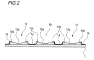
図1は、ウェハレベルレンズの構成の一例を示す平面図である。図2は、図1に示すウェハレベルレンズの構成のA−A線断面図である。
ウェハレベルレンズは、基板1と、該基板1に形成された複数のレンズ10とを有するレンズモジュールを備えている。複数のレンズ10は、基板1に対して1次元又は2次元に配列されている。この構成例では、図1のように、複数のレンズ10が、基板1に対して2次元に配列されている構成を例に説明する。レンズ10は、基板1と同じ材料から構成され、該基板1に成形されたものである。
FIG. 1 is a plan view showing an example of the configuration of a wafer level lens. FIG. 2 is a cross-sectional view taken along the line AA of the configuration of the wafer level lens shown in FIG.
The wafer level lens includes a lens module having a
図2に示すように、レンズ10は、凹状のレンズ面10aと、該レンズ面10aの周囲にレンズ縁部10bとを有する。ここで、レンズ面10aは、レンズ10に入射した光を所望の方向に集光又は発散させる光学的特性を有し、この光学的特性を考慮して曲率や表面形状が設計されている部位の面をいうものとする。この例では、レンズ縁部10bの基板1に対する高さがレンズ面10aの中央よりも高くなるように構成されている。なお、レンズ10の形状は、特に限定されず、例えば、レンズ面10aが凸状に突出した、所謂、凸状レンズとしてもよく、又は非球面のレンズとしてもよい。
As shown in FIG. 2, the
ここでは、基板1の一方の面に複数のレンズ10が設けられた構成を例示しているが、基板1の両方の面に複数のレンズ10が設けられた構成としてもよい。基板1の両方の面に複数のレンズ10が設ける場合には、一方の面の各レンズの光軸が、他方の面の各レンズの光軸と一致するように成形される。
Here, a configuration in which a plurality of
図2では、ウェハレベルレンズは、基板1に複数のレンズ10が成形されたレンズモジュールを1つ有する構成としたが、レンズモジュールを2つ以上重ね合わせた構成としてもよい。
In FIG. 2, the wafer level lens has one lens module in which a plurality of
ウェハレベルレンズは、レンズ10のレンズ縁部10bの表面と、レンズ10同士の間の基板1の表面とを覆うように黒色レジスト層14が設けられている。黒色レジスト層14は、レンズモジュールの表面において、前記レンズのレンズ面10aを除く領域にパターニングされたものである。ウェハレベルレンズがレンズモジュールを2つ以上重ね合わせた構成の場合、少なくとも1つのレンズモジュールの表面に黒色レジスト層14が備えられる。黒色レジスト層14は、レンズ10の光軸と交差する部分が開口するパターンで形成されている。なお、黒色レジスト層14は、その一部がレンズ面10aの周縁部に被さっていてもよい。
黒色レジスト層14、光反射率が金属層などに比べて低いため、光反射に伴うゴーストやフレア等の不都合を低減できる。黒色レジスト層は、黒色レジスト組成物を用いて形成される。黒色レジスト組成物については後述する。
The wafer level lens is provided with a
Since the
図3は、ウェハレベルレンズの他の構成例を示す断面図である。
この例では、基板1の一方の面に図2と同様の形状のレンズ10が成形され、他方の面に凸状のレンズ20が成形されている。また、他方の面には、レンズモジュール同士を重ね合わせる際に距離を確保するためのスペーサが形成されている。スペーサ12は、平面視において格子状の部材であって、基板1の他方の面に接合される。この例では、レンズモジュールの基板1にスペーサを接合した後、ダイシングによって、基板1にレンズ10及びレンズ20が1個づつ備えられた構成となるように分離したものである。スペーサ12は、基板1の一部として該基板1に一体に成形されたものとしてもよい。
FIG. 3 is a cross-sectional view showing another configuration example of the wafer level lens.
In this example, a
図4は、撮像ユニットの構成の一例を示す断面図である。
撮像ユニットは、ウェハレベルレンズをダイシングしてレンズごとに分離したレンズモジュールと、撮像素子(ここでは、固体撮像素子)Dと、固体撮像素子Dが設けられたセンサ基板Wとを備える。この例の撮像ユニットは、3つのレンズモジュールLM1,LM2,LM3を光の入射側(図4の上側)からのこの順に重ね合わせた構成である。
FIG. 4 is a cross-sectional view illustrating an example of the configuration of the imaging unit.
The imaging unit includes a lens module obtained by dicing a wafer level lens and separating each lens, an imaging element (here, a solid-state imaging element) D, and a sensor substrate W provided with the solid-state imaging element D. The imaging unit of this example has a configuration in which three lens modules LM1, LM2, and LM3 are superposed in this order from the light incident side (upper side in FIG. 4).
レンズモジュールLM1は、基板1Aの上側の面に凸状のレンズ10Aが成形され、下側の面に凹状のレンズ面を有するレンズ20Aが成形されている。基板1Aの上側の面には、レンズ10Aのレンズ面を除く領域にパターニングされた黒色レジスト層14が設けられている。レンズ20Aには、レンズ面を除く領域にパターニングされた黒色レジスト層14が設けられている。黒色レジスト層14のパターンの形状は限定されず、黒色レジスト層14は、レンズ10A,20Aの光軸と交差する部分が開口するパターンで形成されていればよく、レンズモジュールLM2,3における黒色レジスト層14についても同様である。
In the lens module LM1, a
レンズモジュールLM2は、基板1Bの上側の面に凹状のレンズ10Bが成形され、下側の面に凸状のレンズ面を有するレンズ20Bが成形されている。このレンズモジュールLM2は図3に示す構成と基本的に同じである。レンズモジュールLM2の光入射側の表面における、レンズ10Bのレンズ面を除く領域、つまり、レンズ縁部及び基板1B表面のレンズ10Bが設けられていない領域にパターニングされた黒色レジスト層14が設けられている。この例ではレンズモジュールLM2の反対側の表面には黒色レジスト層14を設けていないが、レンズ20Bのレンズ面を除く領域にパターニングされた黒色レジスト層14を設けてもよい。
In the lens module LM2, a
レンズモジュールLM3は、基板1Cの上側の面に非球面形状のレンズ10Cが成形され、下側の面に非球面形状のレンズ面を有するレンズ20Cが成形されている。レンズモジュールLM3の両方の面において、レンズ10C及びレンズ20Cのレンズ面を除く領域にパターニングされた黒色レジスト層14が設けられている。
In the lens module LM3, an
なお、レンズ10A,10B,10C,20A,20B,20Cは、いずれも光軸に対して回転対称となる形状で設けられている。レンズモジュールLM1,LM2,LM3は、全てのレンズ10A,10B,10C,20A,20B,20Cの光軸が一致するように、スペーサ12を介して接合されている。
The
レンズモジュールLM1,LM2,LM3は、スペーサ12を介して互いに接合され、レンズモジュールLM3はスペーサ12を介してセンサ基板Wに接合される。レンズモジュールLM1,LM2,LM3のレンズ10A,10B,10C,20A,20B,20Cは、センサ基板Wに設けられた固体撮像素子Dに被写体像を結像させる。
The lens modules LM1, LM2, and LM3 are bonded to each other via the
センサ基板Wは、例えばシリコンなどの半導体材料で形成されたウェハを平面視略矩形状に切り出して成形されている。固体撮像素子Dは、センサ基板Wの略中央部に設けられている。固体撮像素子Dは、例えばCCDイメージセンサやCMOSイメージセンサである。固体撮像素子Dは、チップ化された後で、配線等が形成された半導体基板上にボンディングした構成とすることができる。又は、固体撮像素子Dは、センサ基板Wに対して周知の成膜工程、フォトリソグラフィ工程、エッチング工程、不純物添加工程等を行い、該センサ基板Wに電極、絶縁膜、配線等を形成して構成されてもよい。 The sensor substrate W is formed by cutting a wafer formed of a semiconductor material such as silicon into a substantially rectangular shape in plan view. The solid-state imaging device D is provided at a substantially central portion of the sensor substrate W. The solid-state image sensor D is, for example, a CCD image sensor or a CMOS image sensor. The solid-state imaging device D can be configured to be bonded on a semiconductor substrate on which wirings and the like are formed after being formed into a chip. Alternatively, the solid-state imaging device D performs a well-known film formation process, photolithography process, etching process, impurity addition process, etc. on the sensor substrate W, and forms electrodes, insulating films, wirings, etc. on the sensor substrate W. It may be configured.
レンズモジュールLM3のスペーサ12とセンサ基板Wとは、例えば接着剤などを用いて接合される。各スペーサ12は、レンズモジュールLM1,LM2,LM3のレンズ10A,10B,10C,20A,20B,20Cが固体撮像素子D上で被写体像を結像させるように設計されている。また、各スペーサ12は、レンズ10A,10B,10C,20A,20B,20Cが、重なり合うレンズモジュールLM1,LM2,LM3同士、又は、レンズモジュールLM3とセンサ基板Wとが互いに接触しないように、それぞれの間に所定の距離を隔てる高さ(基板の面に対して垂直方向の長さ)で形成されている。
The
スペーサ12は、レンズモジュールLM1,LM2,LM3同士を、又は、レンズモジュールLM3とセンサ基板Wとの間隔を所定の距離を隔てた位置関係で保持できる範囲で、その形状は特に限定されず適宜変形することができる。例えば、スペーサ12は、基板1A,1B,1Cの4隅にそれぞれ設けられる柱状の部材であってもよい。また、スペーサ12は、固体撮像素子Dの周囲を取り囲むような枠状の部材であってもよい。固体撮像素子Dを枠状のスペーサ12によって取り囲むことで外部から隔絶すれば、固体撮像素子Dにレンズを透過する光以外の光が入射しないように遮光することができる。また、固体撮像素子Dを外部から密封することで、固体撮像素子Dに塵埃が付着することを防止できる。
The
図4に示すように、レンズモジュールLM1,LM2,LM3を複数重ね合わせた構成とする場合には、光入射側に最も近い最上部のレンズモジュールLM1における表面又は基板1Aにおける表面には、黒色レジスト層14のかわりに反射層を設けてもよい。反射層は、可視光(波長400−700nm)に対して反射率が4%以下であって、透過率が0.1%以下とすることが好ましい。反射材料としては、クロム(Cr)、金、タングステン、アルミ、銅、ニッケル、亜鉛、銀などの金属又は金属材料を用いることが好ましい。
As shown in FIG. 4, when a plurality of lens modules LM1, LM2, and LM3 are stacked, a black resist is formed on the surface of the uppermost lens module LM1 closest to the light incident side or the surface of the
以上のように構成された撮像ユニットは、携帯端末等に内蔵される図示しない回路基板にリフロー実装される。回路基板には、撮像ユニットが実装される位置に予めペースト状の半田が適宜印刷されており、そこに撮像ユニットが載せられ、この撮像ユニットを含む回路基板に赤外線の照射や熱風の吹付けといった加熱処理が施され、撮像ユニットが回路基板に溶着される。 The imaging unit configured as described above is reflow-mounted on a circuit board (not shown) built in a portable terminal or the like. The circuit board is preliminarily printed with paste-like solder at a position where the imaging unit is mounted, and the imaging unit is mounted on the circuit board. The circuit board including the imaging unit is irradiated with infrared rays or hot air is blown. Heat treatment is performed, and the imaging unit is welded to the circuit board.
次に、黒色レジスト層14に含まれる黒色レジスト組成物について説明する。
Next, the black resist composition contained in the black resist
[黒色レジスト組成物]
本発明の黒色レジスト組成物は、黒色材料を含有する。
黒色材料としては、公知の着色剤、金属粒子、又は金属を含有する粒子を用いることができる。着色剤としては黒色顔料、染料を用いることができる。また、種々の色相の着色剤を混合して所望の透過率を有する黒色レジスト組成物を調整しても良い。それら着色剤としては、特開2006−208796号公報の段落番号[0037]〜[0046]などに記載の公知の着色剤及びそれらの組み合わせを用いることができる。中でも、遮光性が高いという観点から、カーボンブラック、チタンカーボン、酸化鉄、酸化チタン、黒鉛、銀錫、銀コロイドなどが好ましく、中でも、遮光性の点でカーボンブラック、銀錫、チタンブラックが特に好ましい。これらの黒色材料を分散し、その他硬化成分等と組み合わせて組成物として使用する。
[Black resist composition]
The black resist composition of the present invention contains a black material.
As the black material, a known colorant, metal particles, or particles containing a metal can be used. As the colorant, a black pigment or a dye can be used. Moreover, you may adjust the black resist composition which has a desired transmittance | permeability by mixing the coloring agent of various hues. As these colorants, known colorants described in paragraph numbers [0037] to [0046] of JP-A-2006-208796 and combinations thereof can be used. Among these, carbon black, titanium carbon, iron oxide, titanium oxide, graphite, silver tin, silver colloid, and the like are preferable from the viewpoint of high light shielding properties, and carbon black, silver tin, and titanium black are particularly preferable in terms of light shielding properties. preferable. These black materials are dispersed and used as a composition in combination with other curing components.
カーボンブラックの例としては、Pigment Black(ピグメント・ブラック)7(カーボンブラックC.I.No.77266)が好ましい。市販品として、三菱カーボンブラック MA100(三菱化学(株)製)、三菱カーボンブラック#5(三菱化学(株)製)が挙げられる。 As an example of carbon black, Pigment Black 7 (carbon black CI No. 77266) is preferable. Commercially available products include Mitsubishi Carbon Black MA100 (manufactured by Mitsubishi Chemical Corporation) and Mitsubishi Carbon Black # 5 (manufactured by Mitsubishi Chemical Corporation).
チタンブラックの例としては、TiO、TiNやこれらを有する混合物が好ましい。市販品として、三菱マテリアルズ(株)製の(商品名)12Sや13Mが挙げられる。チタンブラックの平均一次粒径は、5〜100nmが好ましく、10〜100nmが更に好ましく、10〜50nmが特に好ましい。チタンブラックの比表面積は、とくに限定がないが、かかるチタンブラックを撥水化剤で表面処理した後の撥水性が所定の性能となるために、BET法にて測定した値が通常5〜150m2/g程度、特に20〜100m2/g程度であることが好ましい。 As an example of titanium black, TiO, TiN, and a mixture containing these are preferable. Examples of commercially available products include (trade names) 12S and 13M manufactured by Mitsubishi Materials Corporation. The average primary particle size of titanium black is preferably 5 to 100 nm, more preferably 10 to 100 nm, and particularly preferably 10 to 50 nm. The specific surface area of titanium black is not particularly limited, but the water repellency after surface treatment of such titanium black with a water repellent becomes a predetermined performance. 2 / g approximately, and preferably from 20 to 100 m 2 / g approximately.
黒鉛の例としては、平均一次粒子径がストークス径で3μm以下のものが好ましい。平均一次粒子径が前記範囲内であると、遮光パターンの輪郭形状が均一になり、シャープネスが良好になる。また、90%以上の粒子の平均一次粒子径が0.1μm以下であることが望ましい。具体的には、遠心分離等の区分操作で平均一次粒子径を振るい分けした粒子などを使用できる。 As an example of graphite, an average primary particle diameter of Stokes diameter of 3 μm or less is preferable. When the average primary particle size is within the above range, the contour shape of the light shielding pattern becomes uniform, and the sharpness is improved. Moreover, it is desirable that the average primary particle diameter of 90% or more of the particles is 0.1 μm or less. Specifically, particles having an average primary particle diameter distributed by a sorting operation such as centrifugation can be used.
更には、遮光性が高いという点で、黒色剤として、金属粒子又は金属を有する粒子を用いることが好ましい。金属粒子又は金属を有する粒子としては、特に限定されず、いかなるものを用いてもよい。金属粒子又は金属を有する粒子としては、2種以上の金属を組み合わせて用いてもよく、合金として用いることも可能である。また、金属と金属化合物との複合粒子でもよい。 Furthermore, it is preferable to use metal particles or metal-containing particles as the blacking agent in terms of high light shielding properties. It does not specifically limit as a metal particle or the particle | grains which have a metal, What kind of thing may be used. As metal particles or metal-containing particles, two or more kinds of metals may be used in combination, or an alloy may be used. Moreover, the composite particle of a metal and a metal compound may be sufficient.
金属粒子として、特開2006−251237号公報の段落番号[0037]〜[0054]に記載の粒子や合金が好適に挙げられる。具体的には、形状異方性金属微粒子が挙げられる。形状異方性金属微粒子は、形状異方性を有する球状以外の形状であれば制限はなく、好ましくは、ペレット状、ジャガイモ状等の不定形、棒状(針状、円柱形、直方体等の角柱形、ラグビーボール型等)、平板状(鱗片状、楕円板状、板状)、繊維状、金平糖状、コイル状等の金属微粒子である。粒子形状には制限はないが、より好ましくは棒状、不定形、板状である。 Suitable examples of the metal particles include particles and alloys described in paragraph numbers [0037] to [0054] of JP-A-2006-251237. Specifically, shape anisotropic metal fine particles are exemplified. The shape anisotropic metal fine particle is not limited as long as it has a shape other than a spherical shape having shape anisotropy, and is preferably an irregular shape such as a pellet shape or a potato shape, or a rod shape (a needle shape, a cylindrical shape, a rectangular shape such as a rectangular parallelepiped). Shape, rugby ball type, etc.), flat plate shape (scale, oval plate, plate shape), fiber, confetti, coil, etc. Although there is no restriction | limiting in a particle shape, More preferably, it is rod shape, an indeterminate form, and plate shape.
金属粒子又は金属を有する粒子としては、金属又は、金属と金属化合物とから形成されるものが好ましく、金属から形成されるものが特に好ましい。 As the metal particles or metal-containing particles, those formed from a metal or a metal and a metal compound are preferable, and those formed from a metal are particularly preferable.
特に長周期律表(IUPAC1991)の第4周期、第5周期、及び第6周期からなる群から選ばれる金属を主成分として含むことが好ましい。また、第2〜14族からなる郡から選ばれる金属を含有することが好ましく、第2族、第8族、第9族、第10族、第11族、第12族、第13族、及び第14族からなる群から選ばれる金属を主成分として含むことがより好ましい。これらの金属のうち、金属粒子としては、第4周期、第5周期、又は第6周期の金属であって、第2族、第10族、第11族、第12族、又は第14族の金属の粒子が更に好ましい。
In particular, a metal selected from the group consisting of the fourth period, the fifth period, and the sixth period of the long periodic table (IUPAC 1991) is preferably included as a main component. Moreover, it is preferable to contain the metal chosen from the group which consists of 2-14 groups, 2nd group, 8th group, 9th group, 10th group, 11th group, 12th group, 13th group, and More preferably, a metal selected from the group consisting of
金属粒子として好ましい例は、銅、銀、金、白金、パラジウム、ニッケル、錫、コバルト、ロジウム、イリジウム、鉄、カルシウム、ルテニウム、オスミウム、マンガン、モリブデン、タングステン、ニオブ、タンテル、チタン、ビスマス、アンチモン、鉛、及びこれらの合金から選ばれる少なくとも1種を挙げることができる。更に好ましい金属は、銅、銀、金、白金、パラジウム、ニッケル、錫、コバルト、ロジウム、カルシウム、イリジウム、及びこれらの合金、より好ましい金属は、銅、銀、金、白金、パラジウム、錫、カルシウム、及びこれらの合金から選ばれる少なくとも1種であり、特に好ましい金属は、銅、銀、金、白金、錫、及びこれらの合金から選ばれる少なくとも1種である。とりわけ銀が好ましく(銀としてはコロイド銀が好ましい)、銀錫合金部を有する粒子が最も好ましい。 Preferred examples of the metal particles include copper, silver, gold, platinum, palladium, nickel, tin, cobalt, rhodium, iridium, iron, calcium, ruthenium, osmium, manganese, molybdenum, tungsten, niobium, tantel, titanium, bismuth, and antimony. And at least one selected from lead, and alloys thereof. More preferable metals are copper, silver, gold, platinum, palladium, nickel, tin, cobalt, rhodium, calcium, iridium, and alloys thereof, and more preferable metals are copper, silver, gold, platinum, palladium, tin, and calcium. And at least one selected from these alloys, and particularly preferred metals are at least one selected from copper, silver, gold, platinum, tin, and alloys thereof. In particular, silver is preferable (as colloidal silver is preferable as silver), and particles having a silver-tin alloy part are most preferable.
銀錫の例としては、特開2006−227268号公報,特許第4237148号,特許第4223487号に記載されるような銀錫合金を主成分とし平均粒子系が1nm以上かつ300nm以下の微粒子などが挙げられる。 Examples of silver tin include fine particles having a silver tin alloy as a main component and an average particle system of 1 nm or more and 300 nm or less as described in JP-A No. 2006-227268, Japanese Patent No. 4237148, and Japanese Patent No. 4223487. Can be mentioned.
[金属化合物粒子]
金属化合物とは、前記金属と金属以外の他の元素との化合物である。金属と他の元素との化合物としては、金属の酸化物、硫化物、窒化物、硫酸塩、炭酸塩などが挙げられ、金属化合物粒子としてはこれらの粒子が好適である。中でも、色調や微粒子形成のしやすさから、窒化物、硫化物の粒子が好ましい。
金属化合物の例としては、酸化銅(II)、硫化鉄、硫化銀、硫化銅(II)、チタンブラックなどがあるが、色調、微粒子形成のしやすさや安定性の観点から、硫化銀が特に好ましい。
[Metal compound particles]
The metal compound is a compound of the metal and an element other than the metal. Examples of the compound of metal and other elements include metal oxides, sulfides, nitrides, sulfates, carbonates, and the like, and these particles are suitable as the metal compound particles. Of these, nitride and sulfide particles are preferred because of their color tone and ease of fine particle formation.
Examples of the metal compound include copper oxide (II), iron sulfide, silver sulfide, copper sulfide (II), and titanium black. From the viewpoint of color tone, ease of fine particle formation and stability, silver sulfide is particularly preferable. preferable.
[複合粒子]
複合粒子とは、金属と金属化合物とが結合して1つの粒子になったものをいう。例えば、粒子の内部と表面で組成の異なるもの、2種の粒子が合一したもの等を挙げることができる。また、金属化合物と金属とはそれぞれ1種でも2種以上であってもよい。
金属化合物と金属との複合粒子の具体例としては、銀と硫化銀の複合粒子、銀と酸化銅(II)の複合粒子などが好適に挙げられる。
[Composite particles]
The composite particles are those in which a metal and a metal compound are combined into one particle. For example, the inside of the particle and the surface are different in composition, and the two kinds of particles are combined. Further, each of the metal compound and the metal may be one type or two or more types.
Specific examples of the composite particles of the metal compound and the metal include preferably composite particles of silver and silver sulfide, composite particles of silver and copper (II) oxide, and the like.
本発明に用いられる着色剤として顔料を用いる場合は、予め微細化処理を施したものを使用することが好ましい。顔料1次粒子の微細化は、i)顔料、ii)水溶性の無機塩、iii)該無機塩を実質的に溶解しない水溶性有機溶剤をニーダー等で機械的に混練する方法、いわゆるソルトミリング法などがよく知られている。 When a pigment is used as the colorant used in the present invention, it is preferable to use a pigment that has been previously refined. The primary particles of the pigment are made fine by i) a pigment, ii) a water-soluble inorganic salt, and iii) a method of mechanically kneading a water-soluble organic solvent that does not substantially dissolve the inorganic salt with a kneader, so-called salt milling. Laws are well known.
[溶剤]
本発明の着色剤として顔料を用いる場合は、まず少なくとも一種の溶剤に顔料が分散された顔料分散液を製造することが好ましい。溶剤としては、以下に示される有機溶剤から選択される液体が挙げられ、顔料分散液中に含まれる各成分の溶解性や、レジスト組成物に応用した場合の塗布性などを考慮して選択されるものであり、これら所望の物性を満足すれば基本的に特には限定されないが、安全性を考慮して選ばれることが好ましい。
顔料分散液の調製に好適に用いうる溶剤としては、3−エトキシプロピオン酸メチル、3−エトキシプロピオン酸エチル、エチルセロソルブアセテート、乳酸エチル、ジエチレングリコールジメチルエーテル、酢酸ブチル、3−メトキシプロピオン酸メチル、2−ヘプタノン、シクロヘキサノン、ジエチレングリコールモノエチルエーテルアセテート、ジエチレングリコールモノブチルエーテルアセテート、プロピレングリコールメチルエーテル、プロピレングリコールモノメチルエーテルアセテート(PGMEA)等がより好ましい。
[solvent]
When using a pigment as the colorant of the present invention, it is preferable to first produce a pigment dispersion in which the pigment is dispersed in at least one solvent. Examples of the solvent include liquids selected from the organic solvents shown below, and are selected in consideration of the solubility of each component contained in the pigment dispersion and the coating properties when applied to a resist composition. Basically, it is not particularly limited as long as these desired physical properties are satisfied, but it is preferably selected in consideration of safety.
Solvents that can be suitably used for the preparation of the pigment dispersion include methyl 3-ethoxypropionate, ethyl 3-ethoxypropionate, ethyl cellosolve acetate, ethyl lactate, diethylene glycol dimethyl ether, butyl acetate, methyl 3-methoxypropionate, 2- Heptanone, cyclohexanone, diethylene glycol monoethyl ether acetate, diethylene glycol monobutyl ether acetate, propylene glycol methyl ether, propylene glycol monomethyl ether acetate (PGMEA) and the like are more preferable.
本発明の顔料分散液における溶剤の含有量としては、50質量%〜95質量%が好ましく、50質量%〜90質量%がより好ましい。更に、60〜90質量%が特に好ましく、70質量%〜90質量%が最も好ましい。溶剤の含有量が前記範囲内であることにより、分散安定性の点で有利である。 As content of the solvent in the pigment dispersion liquid of this invention, 50 mass%-95 mass% are preferable, and 50 mass%-90 mass% are more preferable. Furthermore, 60-90 mass% is especially preferable, and 70 mass% -90 mass% is the most preferable. When the content of the solvent is within the above range, it is advantageous in terms of dispersion stability.
[その他の成分]
顔料分散液には、顔料分散液の用途など、目的に応じて、本発明の効果を損なわない限りにおいて他の成分を含有することができる。
顔料分散液は、更に顔料誘導体を含有することが好ましい。特に、酸性基を有する顔料誘導体を含有することで、分散性・分散安定性が飛躍的に向上する。
顔料誘導体が有する酸性基としては、スルホン酸、カルボン酸及びその4級アンモニウム塩が好ましい。また、顔料誘導体が有する塩基性基としては、アミノ基が好ましい。
[Other ingredients]
The pigment dispersion can contain other components depending on the purpose, such as the use of the pigment dispersion, as long as the effects of the present invention are not impaired.
The pigment dispersion preferably further contains a pigment derivative. In particular, by including a pigment derivative having an acidic group, dispersibility and dispersion stability are dramatically improved.
As an acidic group which a pigment derivative has, a sulfonic acid, carboxylic acid, and its quaternary ammonium salt are preferable. Moreover, as a basic group which a pigment derivative has, an amino group is preferable.
顔料誘導体の使用量は特に制限がないが、顔料に対し5〜50質量%用いることが好ましく、10〜30質量%用いることが更に好ましい。 Although there is no restriction | limiting in particular in the usage-amount of a pigment derivative, It is preferable to use 5-50 mass% with respect to a pigment, and it is still more preferable to use 10-30 mass%.
また、分散性を向上させるため高分子材料を併用することも好ましい。高分子材料の具体例としては、BYK Chemie社製「Disperbyk−101(ポリアミドアミン燐酸塩)、107(カルボン酸エステル)、110(酸基を含む共重合物)、130(ポリアミド)、161、162、163、164、165、166、170(高分子共重合物)」、「BYK−P104、P105(高分子量不飽和ポリカルボン酸)、EFKA社製「EFKA4047、4050、4010、4165(ポリウレタン系)、EFKA4330、4340(ブロック共重合体)、4400、4402(変性ポリアクリレート)、5010(ポリエステルアミド)、5765(高分子量ポリカルボン酸塩)、6220(脂肪酸ポリエステル)、6745(フタロシアニン誘導体)、6750(アゾ顔料誘導体)」、味の素ファインテクノ(株)製「アジスパーPB821、PB822」、共栄社化学(株)製「フローレンTG−710(ウレタンオリゴマー)」、「ポリフローNo.50E、No.300(アクリル系共重合体)」、楠本化成(株)製「ディスパロンKS−860、873SN、874、#2150(脂肪族多価カルボン酸)、#7004(ポリエーテルエステル)、DA−703−50、DA−705、DA−725」、花王(株)製「デモールRN、N(ナフタレンスルホン酸ホルマリン重縮合物)、MS、C、SN−B(芳香族スルホン酸ホルマリン重縮合物)」、「ホモゲノールL−18(高分子ポリカルボン酸)」、「エマルゲン920、930、935、985(ポリオキシエチレンノニルフェニルエーテル)」、「アセタミン86(ステアリルアミンアセテート)」、ルーブリゾール社製「ソルスパース5000(フタロシアニン誘導体)、22000(アゾ顔料誘導体)、13240(ポリエステルアミン)、3000、17000、27000(末端部に機能部を有する高分子)、24000、28000、32000、38500(グラフト型高分子)」、日光ケミカル社製「ニッコールT106(ポリオキシエチレンソルビタンモノオレート)、MYS−IEX(ポリオキシエチレンモノステアレート)」(以上、商品名)、などが挙げられる。また、川研ファインケミカル(株)製 ヒノアクトT−8000Eなどの両性分散剤も挙げられる。また、後述する(F)アルカリ可溶性樹脂に記載される高分子化合物等が挙げられる。 It is also preferable to use a polymer material in combination in order to improve dispersibility. Specific examples of the polymer material include “Disperbyk-101 (polyamideamine phosphate), 107 (carboxylic acid ester), 110 (copolymer containing an acid group), 130 (polyamide), 161, 162 manufactured by BYK Chemie. , 163, 164, 165, 166, 170 (polymer copolymer) ”,“ BYK-P104, P105 (high molecular weight unsaturated polycarboxylic acid) ”,“ EFKA 4047, 4050, 4010, 4165 (polyurethane) ”manufactured by EFKA. , EFKA 4330, 4340 (block copolymer), 4400, 4402 (modified polyacrylate), 5010 (polyester amide), 5765 (high molecular weight polycarboxylate), 6220 (fatty acid polyester), 6745 (phthalocyanine derivative), 6750 ( Azo pigment derivatives) ", Noji Fine Techno Co., Ltd. “Azisper PB821, PB822”, Kyoeisha Chemical Co., Ltd. “Floren TG-710 (urethane oligomer)”, “Polyflow No. 50E, No. 300 (acrylic copolymer)”, “Disparon KS-860, 873SN, 874, # 2150 (aliphatic polycarboxylic acid), # 7004 (polyetherester), DA-703-50, DA-705, DA-725” manufactured by Enomoto Kasei Co., Ltd., "Demol RN, N (Naphthalenesulfonic acid formalin polycondensate), MS, C, SN-B (aromatic sulfonic acid formalin polycondensate)", "Homogenol L-18 (polymer polycarboxylic acid) manufactured by Kao Corporation ) "," Emulgen 920, 930, 935, 985 (polyoxyethylene nonyl phenyl ether) "," Acetami 86 (stearylamine acetate), Lubrizol's "Solsperse 5000 (phthalocyanine derivative), 22000 (azo pigment derivative), 13240 (polyesteramine), 3000, 17000, 27000 (polymer having a functional part at the terminal)" , 24000, 28000, 32000, 38500 (graft type polymer) "," Nikkor T106 (polyoxyethylene sorbitan monooleate), MYS-IEX (polyoxyethylene monostearate) "manufactured by Nikko Chemical Co., Ltd. , Etc. In addition, amphoteric dispersants such as Hinoact T-8000E manufactured by Kawaken Fine Chemical Co., Ltd. are also included. Moreover, the high molecular compound etc. which are described in (F) alkali-soluble resin mentioned later are mentioned.
特に、分散性の観点から、側鎖にポリエステル鎖を有する高分子分散剤が好ましく、また、分散性と、フォトリソグラフィー法により形成されたパターンの解像性の観点から、酸基とポリエステル鎖とを有する樹脂が好ましい。顔料分散剤における好ましい酸基としては、吸着性の観点から、pKaが6以下の酸基が好ましく、特にカルボン酸、スルホン酸、リン酸が好ましい。 In particular, from the viewpoint of dispersibility, a polymer dispersant having a polyester chain in the side chain is preferable, and from the viewpoint of dispersibility and resolution of a pattern formed by a photolithography method, an acid group and a polyester chain A resin having is preferred. As a preferable acid group in the pigment dispersant, an acid group having a pKa of 6 or less is preferable from the viewpoint of adsorptivity, and carboxylic acid, sulfonic acid and phosphoric acid are particularly preferable.
以下に、本発明において好ましく用いられる分散樹脂について説明する。
好ましい分散樹脂は、分子内に、水素原子を除いた原子数が40〜10000の範囲であり、ポリエステル構造、ポリエーテル構造、及びポリアクリレート構造から選択されるグラフト鎖を有するグラフト共重合体であり、下記式(1)〜式(5)のいずれかで表される構造単位を含むグラフト共重合体である。
The dispersion resin that is preferably used in the present invention will be described below.
A preferable dispersion resin is a graft copolymer having a graft chain selected from a polyester structure, a polyether structure, and a polyacrylate structure, in which the number of atoms excluding hydrogen atoms is in the range of 40 to 10,000 in the molecule. A graft copolymer containing a structural unit represented by any of the following formulas (1) to (5).

〔式(1)〜式(5)中、X1、X2、X3、X4、X5、及びX6は、それぞれ独立に、水素原子又は1価の有機基を表し、Y1、Y2、Y3、Y4、及びY5は、それぞれ独立に、2価の連結基を表し、Z1、Z2、Z3、Z4、及びZ5は、それぞれ独立に、水素原子又は1価の有機基を表す。Rは、水素原子又は1価の有機基を表し、共重合体中に構造の異なるRが存在していてもよい。n、m、p、q、及びrは、それぞれ1〜500の整数を表す。〕
具体例として、以下に示す化合物が挙げられる。なお、下記例示化合物中、各構造単位に併記される数値(主鎖繰り返し単位に併記される数値)は、当該構造単位の含有量〔質量%(wt%)と記載〕を表す。また、側鎖の繰り返し単位に併記される数値は当該繰り返し部位の繰り返し数を示す。
[In Formula (1) to Formula (5), X 1 , X 2 , X 3 , X 4 , X 5 , and X 6 each independently represent a hydrogen atom or a monovalent organic group, Y 1 , Y 2 , Y 3 , Y 4 and Y 5 each independently represent a divalent linking group, and Z 1 , Z 2 , Z 3 , Z 4 and Z 5 each independently represent a hydrogen atom or Represents a monovalent organic group. R represents a hydrogen atom or a monovalent organic group, and R having a different structure may exist in the copolymer. n, m, p, q, and r each represent an integer of 1 to 500. ]
Specific examples include the following compounds. In addition, in the following exemplary compounds, a numerical value written together with each structural unit (a numerical value written together with the main chain repeating unit) represents the content of the structural unit [described as mass% (wt%)]. Moreover, the numerical value written together with the repeating unit of a side chain shows the repeating number of the said repeating part.
黒色材料として無機顔料を用いる場合には、まず、顔料と分散剤と、適切な溶剤により顔料分散組成物を調整した後、重合性組成物に配合することが分散性向上の観点から好ましい。
なお、黒色材料として、無機顔料や赤外線吸収染料を用いる場合においても、所望の分光を実現すべく、既存の赤、青、緑、黄色、シアン、マゼンタ、グレーなどの色相を有する有機顔料として例示した材料以外の染料から適宜選択して組み合わせて用いてもよい。
そのような顔料分散組成物中における顔料分散剤の含有量としては、顔料分散組成物中の着色剤(黒色顔料及び他の着色剤を含む)の全固形分質量に対して、1質量%〜90質量%が好ましく、3質量%〜70質量%がより好ましい。
In the case of using an inorganic pigment as the black material, it is preferable from the viewpoint of improving dispersibility that the pigment dispersion composition is first adjusted with a pigment, a dispersant, and an appropriate solvent, and then blended into the polymerizable composition.
In addition, even when an inorganic pigment or an infrared absorbing dye is used as the black material, it is exemplified as an existing organic pigment having a hue such as red, blue, green, yellow, cyan, magenta, and gray in order to realize a desired spectrum. The dyes other than the selected materials may be appropriately selected and used in combination.
As content of the pigment dispersant in such a pigment dispersion composition, it is 1 mass%-with respect to the total solid content mass of the coloring agent (a black pigment and another coloring agent are included) in a pigment dispersion composition. 90 mass% is preferable and 3 mass%-70 mass% is more preferable.
これらの高分子材料は、単独で使用してもよく、2種以上を組み合わせて使用してもよい。高分子材料を併用する場合、高分子材料の含有量としては、本発明に係る(A)特定樹脂に対して、1質量%〜100質量%であることが好ましく、3質量%〜80質量%がより好ましく、5質量%〜50質量%が更に好ましい。 These polymer materials may be used alone or in combination of two or more. When the polymer material is used in combination, the content of the polymer material is preferably 1% by mass to 100% by mass with respect to the (A) specific resin according to the present invention, and preferably 3% by mass to 80% by mass. Is more preferable, and 5 mass%-50 mass% is still more preferable.
[感光性成分]
黒色材料に更に感光性成分を加えることにより、黒色レジスト組成物を提供する。黒色レジスト組成物は光により露光部の現像液への溶解性が向上するポジ作用を有する組成物でも、露光部が硬化、あるいは現像液への溶解性が低下するネガ作用の組成物でもどちらでも採用することができる。たとえは感光性成分として、光重合開始剤、エチレン性不飽和二重結合を含有する化合物を添加することで、解像性・色特性・塗布性・現像性に優れた黒色レジスト組成物を提供することができる。
[Photosensitive component]
A black resist composition is provided by further adding a photosensitive component to the black material. The black resist composition is either a positive composition that improves the solubility of the exposed area in the developer by light, or a negative composition that cures the exposed area or decreases the solubility in the developer. Can be adopted. For example, by adding a photopolymerization initiator and a compound containing an ethylenically unsaturated double bond as the photosensitive component, a black resist composition with excellent resolution, color characteristics, coating properties, and developability is provided. can do.
(光重合開始剤)
黒色レジスト組成物は、感度及びパターン形成性向上のため光重合開始剤を含有することが好ましい。本発明における光重合開始剤は、光により分解し、本発明における重合可能な成分の重合を開始、促進する化合物であり、波長300nm〜500nmの領域に吸収を有するものであることが好ましい。また、光重合開始剤は、単独で、又は2種以上を併用して用いることができる。
(Photopolymerization initiator)
The black resist composition preferably contains a photopolymerization initiator for improving sensitivity and pattern formation. The photopolymerization initiator in the present invention is a compound that is decomposed by light and initiates and accelerates polymerization of the polymerizable component in the present invention, and preferably has an absorption in a wavelength region of 300 nm to 500 nm. Moreover, a photoinitiator can be used individually or in combination of 2 or more types.
光重合開始剤としては、露光感度の観点から、トリアジン系化合物、アルキルアミノ化合物、ベンジルジメチルケタール化合物、α−ヒドロキシケトン化合物、α−アミノケトン化合物、アシルホスフィン系化合物、フォスフィンオキサイド系化合物、メタロセン化合物、オキシム系化合物、ビイミダゾール系化合物、オニウム系化合物、ベンゾチアゾール系化合物、ベンゾフェノン系化合物、アセトフェノン系化合物及びその誘導体、シクロペンタジエン−ベンゼン−鉄錯体及びその塩、ハロメチルオキサジアゾール化合物、3−アリール置換クマリン化合物からなる群より選択される化合物が好ましい。 As photopolymerization initiators, from the viewpoint of exposure sensitivity, triazine compounds, alkylamino compounds, benzyldimethyl ketal compounds, α-hydroxyketone compounds, α-aminoketone compounds, acylphosphine compounds, phosphine oxide compounds, metallocene compounds Oxime compounds, biimidazole compounds, onium compounds, benzothiazole compounds, benzophenone compounds, acetophenone compounds and derivatives thereof, cyclopentadiene-benzene-iron complexes and salts thereof, halomethyloxadiazole compounds, 3- Compounds selected from the group consisting of aryl substituted coumarin compounds are preferred.
光重合開始剤は、より好ましくは、トリアジン系化合物、アルキルアミノ化合物、α−アミノケトン化合物、アシルホスフィン系化合物、フォスフィンオキサイド系化合物、オキシム系化合物、ビイミダゾール系化合物、オニウム系化合物、ベンゾフェノン系化合物、アセトフェノン系化合物であり、トリアジン系化合物、アルキルアミノ化合物、オキシム系化合物、ビイミダゾール系化合物からなる群より選ばれる少なくとも一種の化合物が更に好ましく、オキシム系化合物、ビイミダゾール系化合物が最も好ましい。 The photopolymerization initiator is more preferably a triazine compound, an alkylamino compound, an α-aminoketone compound, an acylphosphine compound, a phosphine oxide compound, an oxime compound, a biimidazole compound, an onium compound, or a benzophenone compound. The acetophenone compound is more preferably at least one compound selected from the group consisting of triazine compounds, alkylamino compounds, oxime compounds, and biimidazole compounds, and most preferably oxime compounds and biimidazole compounds.
特に、黒色レジスト組成物は、充分な遮光性を確保するため、処方上、黒色レジスト組成物の顔料濃度が高く、一方で開始剤の添加量は少なくなり、感度が低下してしまう。又、露光をステッパーで行う際には、トリアジン系化合物等のごとく、露光時にハロゲン含有化合物を発生する開始剤を用いると、機器の腐食の原因となり使用し難い。これらを考慮すれば、感度と諸性能を満足させる光重合開始剤としては、オキシム系化合物が好ましく、特に、365nmに吸収を有するオキシム系化合物が最も好ましい。 In particular, since the black resist composition ensures sufficient light-shielding properties, the pigment concentration of the black resist composition is high in the formulation, while the additive amount of the initiator is reduced and the sensitivity is lowered. Further, when exposure is performed with a stepper, if an initiator that generates a halogen-containing compound at the time of exposure, such as a triazine compound, is used, it causes corrosion of the equipment and is difficult to use. Considering these, as the photopolymerization initiator that satisfies the sensitivity and various performances, an oxime compound is preferable, and an oxime compound having absorption at 365 nm is most preferable.
光重合開始剤の含有量は、黒色レジスト組成物の全固形分に対し0.1質量%〜50質量%であることが好ましく、より好ましくは0.5質量%〜30質量%、特に好ましくは1質量%〜20質量%である。この範囲で、良好な感度とパターン形成性が得られる。 The content of the photopolymerization initiator is preferably 0.1% by mass to 50% by mass, more preferably 0.5% by mass to 30% by mass, particularly preferably the total solid content of the black resist composition. 1% by mass to 20% by mass. Within this range, good sensitivity and pattern formability can be obtained.
(エチレン性不飽和二重結合を含有する化合物)
本発明の黒色レジスト組成物は、前記樹脂以外のエチレン性不飽和二重結合を含有する化合物(以下、単に「重合性化合物」と称する場合がある。)を含有することができる。
(Compound containing an ethylenically unsaturated double bond)
The black resist composition of the present invention may contain a compound containing an ethylenically unsaturated double bond other than the resin (hereinafter, sometimes simply referred to as “polymerizable compound”).
エチレン性不飽和二重結合を含有する化合物は、上記樹脂以外のものであって、少なくとも一個のエチレン性不飽和二重結合を有する付加重合性化合物であり、末端エチレン性不飽和結合を少なくとも1個、好ましくは2個以上有する化合物から選ばれる。このような化合物群は当該産業分野において広く知られるものであり、本発明においてはこれらを特に限定無く用いることができる。これらは、例えばモノマー、プレポリマー、すなわち2量体、3量体及びオリゴマー、又はそれらの混合物並びにそれらの共重合体などの化学的形態をもつ。
本発明に好適に用いうる重合性化合物としては、例えば、特開2008−233244号公報の段落番号〔0115〕〜〔0116〕に記載の化合物、及び特開2009−20453号公報の段落番号〔0100〕〜〔0109〕記載の化合物が挙げられ、これらを目的に応じて使用しうる。
The compound containing an ethylenically unsaturated double bond is other than the above resin, and is an addition polymerizable compound having at least one ethylenically unsaturated double bond, and has at least one terminal ethylenically unsaturated bond. It is selected from compounds having, preferably two or more. Such a compound group is widely known in the industrial field, and can be used without any particular limitation in the present invention. These have chemical forms such as monomers, prepolymers, i.e. dimers, trimers and oligomers, or mixtures thereof and copolymers thereof.
Examples of the polymerizable compound that can be suitably used in the present invention include compounds described in paragraphs [0115] to [0116] of JP-A-2008-233244 and paragraph numbers [0100 of JP-A-2009-20453. ] To [0109] can be used, and these can be used according to the purpose.
本発明に用いうる重合性化合物としては、ビスフェノールAジアクリレートEO変性体、ペンタエリスリトールトリアクリレート、ペンタエリスリトールテトラアクリレート、ジペンタエリスリトールペンタアクリレート、ジペンタエリスリトールペンタアクリレートコハク酸変性体、ジペンタエリスリトールヘキサアクリレート、トリ(アクリロイルオキシエチル)イソシアヌレート、ペンタエリスリトールテトラアクリレートEO変性体、ジペンタエリスリトールヘキサアクリレートEO変性体などが好ましく、また、市販品としては、DPHA−40H(日本化薬(株)製)、UA−306H、UA−306T、UA−306I、AH−600、T−600、AI−600(共栄(株)製)が好ましい。 Examples of polymerizable compounds that can be used in the present invention include bisphenol A diacrylate EO-modified, pentaerythritol triacrylate, pentaerythritol tetraacrylate, dipentaerythritol pentaacrylate, dipentaerythritol pentaacrylate succinic acid-modified, dipentaerythritol hexaacrylate. , Tri (acryloyloxyethyl) isocyanurate, pentaerythritol tetraacrylate EO modified product, dipentaerythritol hexaacrylate EO modified product, and the like, and commercially available products include DPHA-40H (manufactured by Nippon Kayaku Co., Ltd.), UA-306H, UA-306T, UA-306I, AH-600, T-600, and AI-600 (manufactured by Kyoei Co., Ltd.) are preferable.
エチレン性不飽和二重結合を含有する化合物の含有量は、黒色レジスト組成物の固形分中に、1質量%〜90質量%であることが好ましく、5質量%〜80質量%であることがより好ましく、10質量%〜70質量%であることが更に好ましい。 The content of the compound containing an ethylenically unsaturated double bond is preferably 1% by mass to 90% by mass and preferably 5% by mass to 80% by mass in the solid content of the black resist composition. More preferably, it is 10 mass%-70 mass%.
黒色レジスト組成物は、更にアルカリ可溶性樹脂を含有することが好ましい。アルカリ可溶性樹脂を含有することにより、現像性・パターン形成性が向上する。 The black resist composition preferably further contains an alkali-soluble resin. By containing an alkali-soluble resin, developability and pattern formation are improved.
[アルカリ可溶性樹脂]
アルカリ可溶性樹脂としては、線状有機高分子重合体であって、分子(好ましくは、アクリル系共重合体、スチレン系共重合体を主鎖とする分子)中に少なくとも1つのアルカリ可溶性を促進する基(例えばカルボキシル基、リン酸基、スルホン酸基、ヒドロキシル基など)を有するアルカリ可溶性樹脂の中から適宜選択することができる。
上記アルカリ可溶性樹脂としては、例えば、特開2008−233244号公報の段落番号〔0096〕〜〔0111〕に記載の樹脂が挙げられる。
アルカリ可溶性樹脂の具体的な構成単位については、特に(メタ)アクリル酸と、これと共重合可能な他の単量体との共重合体、所謂アクリル系樹脂が好適である。
[Alkali-soluble resin]
The alkali-soluble resin is a linear organic polymer, and promotes at least one alkali-solubility in a molecule (preferably a molecule having an acrylic copolymer or a styrene copolymer as a main chain). It can be suitably selected from alkali-soluble resins having a group (for example, carboxyl group, phosphoric acid group, sulfonic acid group, hydroxyl group, etc.).
Examples of the alkali-soluble resin include resins described in paragraph numbers [0096] to [0111] of JP-A-2008-233244.
As a specific structural unit of the alkali-soluble resin, a copolymer of (meth) acrylic acid and another monomer copolymerizable therewith, so-called acrylic resin is particularly preferable.
これらの中では特に、ベンジル(メタ)アクリレート/(メタ)アクリル酸共重合体やベンジル(メタ)アクリレート/(メタ)アクリル酸/他のモノマーからなる多元共重合体が好適である。 Of these, benzyl (meth) acrylate / (meth) acrylic acid copolymers and multi-component copolymers composed of benzyl (meth) acrylate / (meth) acrylic acid / other monomers are particularly suitable.
アクリル系樹脂は、20mgKOH/g〜200mgKOH/gの範囲の酸価を有することが好ましい。この範囲であると現像性、及びパターン形状が良好である。
また、アクリル系樹脂の質量平均分子量Mw(GPC法で測定されたポリスチレン換算値)は、カラーレジストを塗布等の工程上使用しやすい粘度範囲を実現するために、また膜強度を確保するために、2,000〜100,000であることが好ましく、より好ましくは3,000〜50,000である。
アクリル系樹脂の酸価を上記で特定した範囲とするには、各単量体の共重合割合を適切に調整することに容易に行うことができる。また、質量平均分子量の範囲を上記範囲とするには、単量体の共重合の際に、重合方法に応じた連鎖移動剤を適切な量使用することにより容易に行うことができる。
アクリル系樹脂は、例えばそれ自体公知のラジカル重合法により製造することができる。ラジカル重合法でアクリル系樹脂を製造する際の温度、圧力、ラジカル開始剤の種類及びその量、溶媒の種類等々の重合条件は、当業者であれば容易に設定することができるし、条件設定が可能である。
The acrylic resin preferably has an acid value in the range of 20 mgKOH / g to 200 mgKOH / g. Within this range, developability and pattern shape are good.
Also, the mass average molecular weight Mw (polystyrene conversion value measured by GPC method) of the acrylic resin is used to realize a viscosity range that is easy to use in the process of applying a color resist, etc., and to secure film strength. , Preferably from 2,000 to 100,000, more preferably from 3,000 to 50,000.
In order to make the acid value of acrylic resin into the range specified above, it can be easily performed by appropriately adjusting the copolymerization ratio of each monomer. Further, the range of the mass average molecular weight can be easily set by using an appropriate amount of a chain transfer agent according to the polymerization method when the monomers are copolymerized.
The acrylic resin can be produced, for example, by a known radical polymerization method. Polymerization conditions such as temperature, pressure, type and amount of radical initiator, type of solvent, etc. when producing an acrylic resin by radical polymerization can be easily set by those skilled in the art. Is possible.
黒色レジスト組成物にアルカリ可溶性樹脂を添加する際の添加量としては、組成物の全固形分の5質量%〜90質量%であることが好ましく、より好ましくは10質量%〜60質量%である。この範囲であると、膜強度が高くて皮膜性が良く、また画像形成性が良好である。 The addition amount when the alkali-soluble resin is added to the black resist composition is preferably 5% by mass to 90% by mass, more preferably 10% by mass to 60% by mass, based on the total solid content of the composition. . Within this range, the film strength is high, the film property is good, and the image formability is good.
また、本発明における黒色レジスト組成物の架橋効率を向上させるために、重合性基をアルカリ可溶性樹脂に有した樹脂を単独若しくは重合性基を有しないアルカリ可溶性樹脂と併用してもよく、アリール基、(メタ)アクリル基、アリールオキシアルキル基等を側鎖に含有したポリマー等が有用である。
重合性二重結合を有するアルカリ可溶性樹脂は、アルカリ現像液での現像が可能であって、更に光硬化性と熱硬化性を備えたものである。
これら重合性基を含有するポリマーの例を以下に示すが、COOH基、OH基等のアルカリ可溶性基と炭素−炭素間不飽和結合が含まれていれば下記に限定されない。
(1)予めイソシアネート基とOH基を反応させ、未反応のイソシアネート基を1つ残し、かつ(メタ)アクリロイル基を少なくとも1つ含む化合物とカルボキシル基を含むアクリル樹脂との反応によって得られるウレタン変性した重合性二重結合含有アクリル樹脂、
(2)カルボキシル基を含むアクリル樹脂と分子内にエポキシ基及び重合性二重結合を共に有する化合物との反応によって得られる不飽和基含有アクリル樹脂、
(3)酸ペンダント型エポキシアクリレート樹脂、
(4)OH基を含むアクリル樹脂と重合性二重結合を有する2塩基酸無水物を反応させた重合性二重結合含有アクリル樹脂。
上記のうち、特に(1)及び(2)の樹脂が好ましい。
Further, in order to improve the crosslinking efficiency of the black resist composition in the present invention, a resin having a polymerizable group in an alkali-soluble resin may be used alone or in combination with an alkali-soluble resin having no polymerizable group. Polymers containing a (meth) acryl group, an aryloxyalkyl group or the like in the side chain are useful.
The alkali-soluble resin having a polymerizable double bond can be developed with an alkali developer, and further has photocurability and thermosetting properties.
Examples of polymers containing these polymerizable groups are shown below, but are not limited to the following as long as alkali-soluble groups such as COOH groups and OH groups and carbon-carbon unsaturated bonds are included.
(1) Urethane modification obtained by reacting an isocyanate group and an OH group in advance, leaving one unreacted isocyanate group and reacting at least one (meth) acryloyl group with an acrylic resin containing a carboxyl group A polymerizable double bond-containing acrylic resin,
(2) an unsaturated group-containing acrylic resin obtained by a reaction between an acrylic resin containing a carboxyl group and a compound having both an epoxy group and a polymerizable double bond in the molecule;
(3) Acid pendant type epoxy acrylate resin,
(4) A polymerizable double bond-containing acrylic resin obtained by reacting an acrylic resin containing an OH group with a dibasic acid anhydride having a polymerizable double bond.
Among the above, the resins (1) and (2) are particularly preferable.
重合性二重結合を有するアルカリ可溶性樹脂の酸価としては好ましくは30mgKOH/g〜150mgKOH/g、より好ましくは35mgKOH/g〜120mgKOH/gであり、また質量平均分子量Mwとしては好ましくは2,000〜50,000、より好ましくは3,000〜30,000である。
アルカリ可溶性樹脂の市販品としては、例えば、ダイヤナールNRシリーズ(三菱レイヨン(株)製);Photomer 6173(COOH基含有Polyurethane acrylic oligomer、Diamond Shamrock Co.Ltd.,製);ビスコートR−264、KSレジスト106(いずれも大阪有機化学工業(株)製);サイクロマーPシリーズ、プラクセルCF200シリーズ(いずれもダイセル化学工業(株)製);Ebecryl3800(ダイセルユーシービー(株)製)、などが挙げられる。
The acid value of the alkali-soluble resin having a polymerizable double bond is preferably 30 mgKOH / g to 150 mgKOH / g, more preferably 35 mgKOH / g to 120 mgKOH / g, and the mass average molecular weight Mw is preferably 2,000. 50,000 to 50,000, more preferably 3,000 to 30,000.
Commercially available products of alkali-soluble resins include, for example, Dainar NR series (manufactured by Mitsubishi Rayon Co., Ltd.); Photomer 6173 (COOH group-containing Polyurethane acrylic oligomer, manufactured by Diamond Shamrock Co. Ltd.); Biscote R-264, KS Resist 106 (all manufactured by Osaka Organic Chemical Industry Co., Ltd.); Cyclomer P series, Plaxel CF200 series (all manufactured by Daicel Chemical Industries, Ltd.); Ebecryl 3800 (manufactured by Daicel UCB Co., Ltd.) .
[有機溶剤]
本発明における黒色レジスト組成物は、一般には、有機溶剤を用いて構成することができる。有機溶剤は、各成分の溶解性や黒色レジスト組成物の塗布性を満足すれば基本的には特に制限はないが、特に紫外線吸収剤、バインダーの溶解性、塗布性、安全性を考慮して選ばれることが好ましい。また、本発明における黒色レジスト組成物を調製する際には、少なくとも2種類の有機溶剤を含むことが好ましい。
[Organic solvent]
In general, the black resist composition in the present invention can be constituted using an organic solvent. The organic solvent is basically not particularly limited as long as the solubility of each component and the coating property of the black resist composition are satisfied, but in particular, considering the solubility, coating property, and safety of the UV absorber and the binder. It is preferable to be selected. Moreover, when preparing the black resist composition in this invention, it is preferable that at least 2 type of organic solvent is included.
有機溶剤としては、エステル類として、例えば、酢酸エチル、酢酸−n−ブチル、酢酸イソブチル、ギ酸アミル、酢酸イソアミル、酢酸イソブチル、プロピオン酸ブチル、酪酸イソプロピル、酪酸エチル、酪酸ブチル、乳酸メチル、乳酸エチル、オキシ酢酸アルキル(例:オキシ酢酸メチル、オキシ酢酸エチル、オキシ酢酸ブチル(例えば、メトキシ酢酸メチル、メトキシ酢酸エチル、メトキシ酢酸ブチル、エトキシ酢酸メチル、エトキシ酢酸エチル等))、3−オキシプロピオン酸アルキルエステル類(例:3−オキシプロピオン酸メチル、3−オキシプロピオン酸エチル等(例えば、3−メトキシプロピオン酸メチル、3−メトキシプロピオン酸エチル、3−エトキシプロピオン酸メチル、3−エトキシプロピオン酸エチル等))、2−オキシプロピオン酸アルキルエステル類(例:2−オキシプロピオン酸メチル、2−オキシプロピオン酸エチル、2−オキシプロピオン酸プロピル等(例えば、2−メトキシプロピオン酸メチル、2−メトキシプロピオン酸エチル、2−メトキシプロピオン酸プロピル、2−エトキシプロピオン酸メチル、2−エトキシプロピオン酸エチル))、2−オキシ−2−メチルプロピオン酸メチル及び2−オキシ−2−メチルプロピオン酸エチル(例えば、2−メトキシ−2−メチルプロピオン酸メチル、2−エトキシ−2−メチルプロピオン酸エチル等)、ピルビン酸メチル、ピルビン酸エチル、ピルビン酸プロピル、アセト酢酸メチル、アセト酢酸エチル、2−オキソブタン酸メチル、2−オキソブタン酸エチル等、並びに、エーテル類として、例えば、ジエチレングリコールジメチルエーテル、テトラヒドロフラン、エチレングリコールモノメチルエーテル、エチレングリコールモノエチルエーテル、メチルセロソルブアセテート、エチルセロソルブアセテート、ジエチレングリコールモノメチルエーテル、ジエチレングリコールモノエチルエーテル、ジエチレングリコールモノブチルエーテル、プロピレングリコールモノメチルエーテル、プロピレングリコールモノメチルエーテルアセテート、プロピレングリコールモノエチルエーテルアセテート、プロピレングリコールモノプロピルエーテルアセテート等、並びに、ケトン類として、例えば、メチルエチルケトン、シクロヘキサノン、2−ヘプタノン、3−ヘプタノン等、並びに、芳香族炭化水素類として、例えば、トルエン、キシレン等が好適に挙げられる。 Examples of organic solvents include esters such as ethyl acetate, n-butyl acetate, isobutyl acetate, amyl formate, isoamyl acetate, isobutyl acetate, butyl propionate, isopropyl butyrate, ethyl butyrate, butyl butyrate, methyl lactate, and ethyl lactate. , Alkyl oxyacetate (eg, methyl oxyacetate, ethyl oxyacetate, butyl oxyacetate (eg, methyl methoxyacetate, ethyl methoxyacetate, butyl methoxyacetate, methyl ethoxyacetate, ethyl ethoxyacetate)), alkyl 3-oxypropionate Esters (eg, methyl 3-oxypropionate, ethyl 3-oxypropionate, etc. (eg, methyl 3-methoxypropionate, ethyl 3-methoxypropionate, methyl 3-ethoxypropionate, ethyl 3-ethoxypropionate, etc.) )), 2- Xylpropionic acid alkyl esters (eg, methyl 2-oxypropionate, ethyl 2-oxypropionate, propyl 2-oxypropionate, etc. (eg, methyl 2-methoxypropionate, ethyl 2-methoxypropionate, 2-methoxy) Propyl propionate, methyl 2-ethoxypropionate, ethyl 2-ethoxypropionate)), methyl 2-oxy-2-methylpropionate and ethyl 2-oxy-2-methylpropionate (eg 2-methoxy-2- Methyl methyl propionate, ethyl 2-ethoxy-2-methylpropionate, etc.), methyl pyruvate, ethyl pyruvate, propyl pyruvate, methyl acetoacetate, ethyl acetoacetate, methyl 2-oxobutanoate, ethyl 2-oxobutanoate, etc. And as ethers For example, diethylene glycol dimethyl ether, tetrahydrofuran, ethylene glycol monomethyl ether, ethylene glycol monoethyl ether, methyl cellosolve acetate, ethyl cellosolve acetate, diethylene glycol monomethyl ether, diethylene glycol monoethyl ether, diethylene glycol monobutyl ether, propylene glycol monomethyl ether, propylene glycol monomethyl ether acetate, Propylene glycol monoethyl ether acetate, propylene glycol monopropyl ether acetate and the like and ketones such as methyl ethyl ketone, cyclohexanone, 2-heptanone and 3-heptanone and aromatic hydrocarbons such as toluene, Xylene and the like are preferred.
これらの有機溶剤は、紫外線吸収剤及びアルカリ可溶性樹脂の溶解性、塗布面状の改良などの観点から、2種以上を混合することも好ましい。この場合、特に好ましくは、上記の3−エトキシプロピオン酸メチル、3−エトキシプロピオン酸エチル、エチルセロソルブアセテート、乳酸エチル、ジエチレングリコールジメチルエーテル、酢酸ブチル、3−メトキシプロピオン酸メチル、2−ヘプタノン、シクロヘキサノン、エチルカルビトールアセテート、ブチルカルビトールアセテート、プロピレングリコールメチルエーテル、及びプロピレングリコールメチルエーテルアセテートから選択される2種以上で構成される混合溶液である。 It is also preferable to mix two or more kinds of these organic solvents from the viewpoints of solubility of the ultraviolet absorber and the alkali-soluble resin, improvement of the coated surface, and the like. In this case, particularly preferably, the above-mentioned methyl 3-ethoxypropionate, ethyl 3-ethoxypropionate, ethyl cellosolve acetate, ethyl lactate, diethylene glycol dimethyl ether, butyl acetate, methyl 3-methoxypropionate, 2-heptanone, cyclohexanone, ethyl It is a mixed solution composed of two or more selected from carbitol acetate, butyl carbitol acetate, propylene glycol methyl ether, and propylene glycol methyl ether acetate.
有機溶剤の着色硬化性組成物中における含有量は、塗布性の観点から、組成物の全固形分濃度が5〜80質量%になる量とすることが好ましく、5〜60質量%が更に好ましく、10〜50質量%が特に好ましい。 The content of the organic solvent in the colored curable composition is preferably such that the total solid content of the composition is 5 to 80% by mass, more preferably 5 to 60% by mass, from the viewpoint of applicability. 10 to 50% by mass is particularly preferable.
黒色レジスト組成物は、必要に応じて以下に詳述する成分を更に含有してもよい。
[増感剤]
黒色レジスト組成物は、重合開始剤のラジカル発生効率の向上、感光波長の長波長化の目的で、増感剤を含有してもよい。本発明に用いることができる増感剤としては、前記した光重合開始剤に対し、電子移動機構又はエネルギー移動機構で増感させるものが好ましい。本発明に用いることができる増感剤としては、以下に列挙する化合物類に属しており、かつ300nm〜450nmの波長領域に吸収波長を有するものが挙げられる。
The black resist composition may further contain components described in detail below as required.
[Sensitizer]
The black resist composition may contain a sensitizer for the purpose of improving the radical generation efficiency of the polymerization initiator and increasing the photosensitive wavelength. As the sensitizer that can be used in the present invention, those that sensitize the above-mentioned photopolymerization initiator by an electron transfer mechanism or an energy transfer mechanism are preferable. Examples of the sensitizer that can be used in the present invention include those belonging to the compounds listed below and having an absorption wavelength in a wavelength region of 300 nm to 450 nm.
好ましい増感剤の例としては、以下の化合物類に属しており、かつ330nmから450nm域に吸収波長を有するものを挙げることができる。
例えば、多核芳香族類(例えば、フェナントレン、アントラセン、ピレン、ペリレン、トリフェニレン、9,10−ジアルコキシアントラセン)、キサンテン類(例えば、フルオレッセイン、エオシン、エリスロシン、ローダミンB、ローズベンガル)、チオキサントン類(イソプロピルチオキサントン、ジエチルチオキサントン、クロロチオキサントン)、シアニン類(例えばチアカルボシアニン、オキサカルボシアニン)、メロシアニン類(例えば、メロシアニン、カルボメロシアニン)、フタロシアニン類、チアジン類(例えば、チオニン、メチレンブルー、トルイジンブルー)、アクリジン類(例えば、アクリジンオレンジ、クロロフラビン、アクリフラビン)、アントラキノン類(例えば、アントラキノン)、スクアリウム類(例えば、スクアリウム)、アクリジンオレンジ、クマリン類(例えば、7−ジエチルアミノ−4−メチルクマリン)、ケトクマリン、フェノチアジン類、フェナジン類、スチリルベンゼン類、アゾ化合物、ジフェニルメタン、トリフェニルメタン、ジスチリルベンゼン類、カルバゾール類、ポルフィリン、スピロ化合物、キナクリドン、インジゴ、スチリル、ピリリウム化合物、ピロメテン化合物、ピラゾロトリアゾール化合物、ベンゾチアゾール化合物、バルビツール酸誘導体、チオバルビツール酸誘導体、アセトフェノン、ベンゾフェノン、チオキサントン、ミヒラーズケトンなどの芳香族ケトン化合物、N−アリールオキサゾリジノンなどのヘテロ環化合物などが挙げられる。
更に欧州特許第568,993号明細書、米国特許第4,508,811号明細書、同5,227,227号明細書、特開2001−125255号公報、特開平11−271969号公報等に記載の化合物等などが挙げられる。
Examples of preferred sensitizers include those belonging to the following compounds and having an absorption wavelength in the range of 330 nm to 450 nm.
For example, polynuclear aromatics (for example, phenanthrene, anthracene, pyrene, perylene, triphenylene, 9,10-dialkoxyanthracene), xanthenes (for example, fluorescein, eosin, erythrosine, rhodamine B, rose bengal), thioxanthones (Isopropylthioxanthone, diethylthioxanthone, chlorothioxanthone), cyanines (eg thiacarbocyanine, oxacarbocyanine), merocyanines (eg merocyanine, carbomerocyanine), phthalocyanines, thiazines (eg thionine, methylene blue, toluidine blue) , Acridines (eg, acridine orange, chloroflavin, acriflavine), anthraquinones (eg, anthraquinone), squariums (eg Squalium), acridine orange, coumarins (eg 7-diethylamino-4-methylcoumarin), ketocoumarin, phenothiazines, phenazines, styrylbenzenes, azo compounds, diphenylmethane, triphenylmethane, distyrylbenzenes, carbazole , Porphyrins, spiro compounds, quinacridone, indigo, styryl, pyrylium compounds, pyromethene compounds, pyrazolotriazole compounds, benzothiazole compounds, barbituric acid derivatives, thiobarbituric acid derivatives, acetophenone, benzophenone, thioxanthone, Michler's ketone and other aromatics Examples include ketone compounds and heterocyclic compounds such as N-aryloxazolidinones.
Further, European Patent No. 568,993, US Pat. No. 4,508,811, No. 5,227,227, JP-A-2001-125255, JP-A-11-271969, etc. And the like.
[重合禁止剤]
黒色レジスト組成物の製造中あるいは保存中において重合可能なエチレン性不飽和二重結合を有する化合物の不要な熱重合を阻止するために少量の熱重合防止剤を添加することが望ましい。
熱重合防止剤としては、ハイドロキノン、p−メトキシフェノール、ジ−t−ブチル−p−クレゾール、ピロガロール、t−ブチルカテコール、ベンゾキノン、4,4’−チオビス(3−メチル−6−t−ブチルフェノール)、2,2’−メチレンビス(4−メチル−6−t−ブチルフェノール)、N−ニトロソフェニルヒドロキシアミン第一セリウム塩等が挙げられる。
[Polymerization inhibitor]
In order to prevent unnecessary thermal polymerization of a compound having an ethylenically unsaturated double bond that can be polymerized during the production or storage of the black resist composition, it is desirable to add a small amount of a thermal polymerization inhibitor.
As thermal polymerization inhibitors, hydroquinone, p-methoxyphenol, di-t-butyl-p-cresol, pyrogallol, t-butylcatechol, benzoquinone, 4,4'-thiobis (3-methyl-6-t-butylphenol) 2,2′-methylenebis (4-methyl-6-tert-butylphenol), N-nitrosophenylhydroxyamine primary cerium salt and the like.
重合禁止剤の添加量は、全組成物の質量に対して約0.01質量%〜約5質量%が好ましい。また必要に応じて、酸素による重合阻害を防止するためにベヘン酸やベヘン酸アミドのような高級脂肪酸誘導体等を添加して、塗布後の乾燥の過程で感光層の表面に偏在させてもよい。高級脂肪酸誘導体の添加量は、全組成物の約0.5質量%〜約10質量%が好ましい。 The addition amount of the polymerization inhibitor is preferably about 0.01% by mass to about 5% by mass with respect to the mass of the whole composition. If necessary, a higher fatty acid derivative such as behenic acid or behenic acid amide may be added to prevent polymerization inhibition due to oxygen, and it may be unevenly distributed on the surface of the photosensitive layer in the course of drying after coating. . The amount of the higher fatty acid derivative added is preferably about 0.5% by mass to about 10% by mass of the total composition.
[界面活性剤]
黒色レジスト組成物には、塗布性をより向上させる観点から、各種の界面活性剤を添加してもよい。界面活性剤としては、フッ素系界面活性剤、ノニオン系界面活性剤、カチオン系界面活性剤、アニオン系界面活性剤、シリコーン系界面活性剤などの各種界面活性剤を使用できる。
[Surfactant]
Various surfactants may be added to the black resist composition from the viewpoint of further improving coatability. As the surfactant, various surfactants such as a fluorine-based surfactant, a nonionic surfactant, a cationic surfactant, an anionic surfactant, and a silicone-based surfactant can be used.
特に、黒色レジスト組成物は、フッ素系界面活性剤を含有することで、塗布液として調製したときの液特性(特に、流動性)がより向上することから、塗布厚の均一性や省液性をより改善することができる。
即ち、フッ素系界面活性剤を含有する黒色レジスト組成物を適用した塗布液を用いて膜形成する場合においては、被塗布面と塗布液との界面張力を低下させることにより、被塗布面への濡れ性が改善され、被塗布面への塗布性が向上する。このため、少量の液量で数μm程度の薄膜を形成した場合であっても、厚みムラの小さい均一厚の膜形成をより好適に行える点で有効である。
In particular, since the black resist composition contains a fluorosurfactant, the liquid properties (particularly fluidity) when prepared as a coating liquid are further improved, so that the coating thickness uniformity and liquid-saving properties are improved. Can be improved more.
That is, in the case of forming a film using a coating liquid to which a black resist composition containing a fluorine-based surfactant is applied, by reducing the interfacial tension between the coated surface and the coating liquid, The wettability is improved and the coating property to the coated surface is improved. For this reason, even when a thin film of about several μm is formed with a small amount of liquid, it is effective in that it is possible to more suitably form a film having a uniform thickness with small thickness unevenness.
フッ素系界面活性剤中のフッ素含有率は、3質量%〜40質量%が好適であり、より好ましくは5質量%〜30質量%であり、特に好ましくは7質量%〜25質量%である。フッ素含有率がこの範囲内であるフッ素系界面活性剤は、塗布膜の厚さの均一性や省液性の点で効果的であり、黒色レジスト組成物中における溶解性も良好である。 The fluorine content in the fluorosurfactant is preferably 3% by mass to 40% by mass, more preferably 5% by mass to 30% by mass, and particularly preferably 7% by mass to 25% by mass. A fluorine-based surfactant having a fluorine content in this range is effective in terms of uniformity of coating film thickness and liquid-saving properties, and has good solubility in a black resist composition.
フッ素系界面活性剤としては、例えば、メガファックF171、同F172、同F173、同F176、同F177、同F141、同F142、同F143、同F144、同R30、同F437、同F475、同F479、同F482、同F554、同F780、同F781(以上、DIC(株)製)、フロラードFC430、同FC431、同FC171(以上、住友スリーエム(株)製)、サーフロンS−382、同SC−101、同SC−103、同SC−104、同SC−105、同SC1068、同SC−381、同SC−383、同S393、同KH−40(以上、旭硝子(株)製)、ソルスパース20000(日本ルーブリゾール(株))等が挙げられる。 Examples of the fluorosurfactant include Megafac F171, F172, F173, F176, F176, F177, F141, F142, F143, F144, R30, F437, F475, F479, F482, F554, F780, F780, F781 (above DIC Corporation), Florard FC430, FC431, FC171 (above, Sumitomo 3M Limited), Surflon S-382, SC-101, Same SC-103, Same SC-104, Same SC-105, Same SC1068, Same SC-381, Same SC-383, Same S393, Same KH-40 (above, manufactured by Asahi Glass Co., Ltd.), Solsperse 20000 (Japan Rouble) Zole Co., Ltd.).
ノニオン系界面活性剤として具体的には、グリセロール、トリメチロールプロパン、トリメチロールエタン並びにそれらのエトキシレート及びプロポキシレート(例えば、グリセロールプロポキシレート、グリセリンエトキシレート等)、ポリオキシエチレンラウリルエーテル、ポリオキシエチレンステアリルエーテル、ポリオキシエチレンオレイルエーテル、ポリオキシエチレンオクチルフェニルエーテル、ポリオキシエチレンノニルフェニルエーテル、ポリエチレングリコールジラウレート、ポリエチレングリコールジステアレート、ソルビタン脂肪酸エステル(BASF社製のプルロニックL10、L31、L61、L62、10R5、17R2、25R2、テトロニック304、701、704、901、904、150R1等が挙げられる。 Specific examples of nonionic surfactants include glycerol, trimethylolpropane, trimethylolethane, and ethoxylates and propoxylates thereof (for example, glycerol propoxylate, glycerin ethoxylate, etc.), polyoxyethylene lauryl ether, polyoxyethylene Stearyl ether, polyoxyethylene oleyl ether, polyoxyethylene octylphenyl ether, polyoxyethylene nonylphenyl ether, polyethylene glycol dilaurate, polyethylene glycol distearate, sorbitan fatty acid ester (Pluronic L10, L31, L61, L62 manufactured by BASF, 10R5, 17R2, 25R2, Tetronic 304, 701, 704, 901, 904, 150R1, etc. It is.
カチオン系界面活性剤として具体的には、フタロシアニン誘導体(商品名:EFKA−745、森下産業(株)製)、オルガノシロキサンポリマーKP341(信越化学工業(株)製)、(メタ)アクリル酸系(共)重合体ポリフローNo.75、No.90、No.95(共栄社油脂化学工業(株)製)、W001(裕商(株)製)等が挙げられる。 Specific examples of the cationic surfactant include phthalocyanine derivatives (trade name: EFKA-745, manufactured by Morishita Sangyo Co., Ltd.), organosiloxane polymer KP341 (manufactured by Shin-Etsu Chemical Co., Ltd.), (meth) acrylic acid ( Co) polymer polyflow no. 75, no. 90, no. 95 (manufactured by Kyoeisha Yushi Chemical Co., Ltd.), W001 (manufactured by Yusho Co., Ltd.), and the like.
アニオン系界面活性剤として具体的には、W004、W005、W017(裕商(株)製)等が挙げられる。 Specific examples of the anionic surfactant include W004, W005, W017 (manufactured by Yusho Co., Ltd.) and the like.
シリコーン系界面活性剤としては、例えば、東レ・ダウコーニング(株)製「トーレシリコーンDC3PA」、「トーレシリコーンSH7PA」、「トーレシリコーンDC11PA」,「トーレシリコーンSH21PA」,「トーレシリコーンSH28PA」、「トーレシリコーンSH29PA」、「トーレシリコーンSH30PA」、「トーレシリコーンSH8400」、モメンティブ・パフォーマンス・マテリアルズ社製「TSF−4440」、「TSF−4300」、「TSF−4445」、「TSF−4460」、「TSF−4452」、信越化学工業(株)製「KP341」、「KF6001」、「KF6002」、ビックケミー社製「BYK307」、「BYK323」、「BYK330」等が挙げられる。界面活性剤は、1種のみを用いてもよいし、2種類以上を組み合わせてもよい。 Examples of the silicone surfactant include “Toray Silicone DC3PA”, “Toray Silicone SH7PA”, “Toray Silicone DC11PA”, “Tore Silicone SH21PA”, “Tore Silicone SH28PA”, “Toray Silicone” manufactured by Toray Dow Corning Co., Ltd. “Silicone SH29PA”, “Toresilicone SH30PA”, “Toresilicone SH8400”, “TSF-4440”, “TSF-4300”, “TSF-4445”, “TSF-4460”, “TSF” manufactured by Momentive Performance Materials, Inc. -4552 ”,“ KP341 ”,“ KF6001 ”,“ KF6002 ”manufactured by Shin-Etsu Chemical Co., Ltd.,“ BYK307 ”,“ BYK323 ”,“ BYK330 ”manufactured by BYK Chemie. Only one type of surfactant may be used, or two or more types may be combined.
界面活性剤の添加量は、黒色レジスト組成物の全質量に対して、0.001質量%〜2.0質量%が好ましく、より好ましくは0.005質量%〜1.0質量%である。 The addition amount of the surfactant is preferably 0.001% by mass to 2.0% by mass, and more preferably 0.005% by mass to 1.0% by mass with respect to the total mass of the black resist composition.
[その他の添加剤]
更に、硬化皮膜の物性を改良するために無機充填剤や、可塑剤、支持体密着性を向上させうる支持体密着剤を加えてもよい。
可塑剤としては例えばジオクチルフタレート、ジドデシルフタレート、トリエチレングリコールジカプリレート、ジメチルグリコールフタレート、トリクレジルホスフェート、ジオクチルアジペート、ジブチルセバケート、トリアセチルグリセリン等があり、結合剤を使用した場合、エチレン性不飽和二重結合を有する化合物と結合剤との合計質量に対し10質量%以下添加することができる。
[Other additives]
Furthermore, in order to improve the physical properties of the cured film, an inorganic filler, a plasticizer, and a support adhesive that can improve the support adhesion may be added.
Examples of plasticizers include dioctyl phthalate, didodecyl phthalate, triethylene glycol dicaprylate, dimethyl glycol phthalate, tricresyl phosphate, dioctyl adipate, dibutyl sebacate, and triacetyl glycerin. 10 mass% or less can be added with respect to the total mass of the compound which has an ionic unsaturated double bond, and a binder.
黒色レジスト組成物を支持体等の硬質材料表面に適用する場合には、該硬質材料表面との密着性を向上させるための添加剤(以下、「支持体密着剤」と称する。)を加えてもよい。
支持体密着剤としては、公知の材料を用いることができるが、特にシラン系カップリング剤、チタネート系カップリング剤、アルミニウム系カップリング剤を用いることが好ましい。
When the black resist composition is applied to the surface of a hard material such as a support, an additive for improving the adhesion to the surface of the hard material (hereinafter referred to as “support adhesion agent”) is added. Also good.
A known material can be used as the support adhesion agent, but it is particularly preferable to use a silane coupling agent, a titanate coupling agent, or an aluminum coupling agent.
シラン系カップリング剤としては、例えば、γ−メタクリロキシプロピルトリメトキシシラン、γ−メタクリロキシプロピルトリエトキシシラン、γ−アクリロキシプロピルトリメトキシシラン、γ−アクリロキシプロピルトリエトキシシラン、γ−メルカプトプロピルトリメトキシシラン、γ−アミノプロピルトリエトキシシラン、フェニルトリメトキシシラン、が好ましく、γ−メタクリロキシプロピルトリメトキシシランが最も好ましい。 Examples of the silane coupling agent include γ-methacryloxypropyltrimethoxysilane, γ-methacryloxypropyltriethoxysilane, γ-acryloxypropyltrimethoxysilane, γ-acryloxypropyltriethoxysilane, and γ-mercaptopropyl. Trimethoxysilane, γ-aminopropyltriethoxysilane, and phenyltrimethoxysilane are preferable, and γ-methacryloxypropyltrimethoxysilane is most preferable.
支持体密着剤の含有量は、黒色レジスト組成物の未露光部に残渣が残らないようにする観点から、本発明の黒色レジスト組成物の全固形分に対して、0.1質量%以上30質量%以下であることが好ましく、0.5質量%以上20質量%以下であることがより好ましく、1質量%以上10質量%以下であることが特に好ましい。 The content of the support adhesion agent is 0.1% by mass or more and 30% with respect to the total solid content of the black resist composition of the present invention, from the viewpoint of leaving no residue in the unexposed portion of the black resist composition. It is preferably at most mass%, more preferably at least 0.5 mass% and at most 20 mass%, particularly preferably at least 1 mass% and at most 10 mass%.
ウェハレベルレンズは、黒色レジスト層14の光反射率が金属等からなる層に比べて低い。このため、黒色レジスト層14によって十分に遮光しつつ、反射光に伴うゴーストやフレア等の不具合を低減できる。例えば、波長400〜700nmの可視光に対する反射率が2%以下であって、透過率が1%以下とすることにより、上記効果を得ることができる。このような物性を有する黒色レジスト層14は、上述の黒色レジスト組成物を用いて形成することによって達成される。
本発明の反射率は、所望の基板上に塗布し、分光光度計で測定することができる。可視光(400−700nm)の反射光を測定する。反射光は低いほど好ましいが、平均値が2%以下、好ましくは反射率が1.5%以下である。
In the wafer level lens, the light reflectance of the black resist
The reflectance of the present invention can be applied to a desired substrate and measured with a spectrophotometer. The reflected light of visible light (400-700 nm) is measured. The lower the reflected light, the better, but the average value is 2% or less, preferably the reflectance is 1.5% or less.
次に、上述したウェハレベルレンズを製造する手順の好ましい例を説明する。なお、以下に説明する実施形態において、すでに説明した部材などと同等な構成・作用を有する部材等については、図中に同一符号又は相当符号を付すことにより、説明を簡略化或いは省略する。 Next, a preferred example of the procedure for manufacturing the wafer level lens described above will be described. In the embodiments described below, members having the same configuration / action as those already described are denoted by the same or corresponding reference numerals in the drawings, and description thereof is simplified or omitted.
図5は、基板にレンズとなる成形材料を供給している状態を示す図である。図6A〜図6Cは、基板にレンズを型で成形する手順を示す図である。 FIG. 5 is a diagram showing a state in which a molding material to be a lens is supplied to the substrate. 6A to 6C are diagrams illustrating a procedure for forming a lens on a substrate with a mold.
レンズ10を形成する材料としては、例えばガラスを用いることができる。ガラスは種類が豊富であり、高屈折率を有するものを選択できるので、大きなパワーを持たせたいレンズの素材として適している。また、ガラスは耐熱性に優れ、上述した撮像ユニットのリフロー実装に好適である。
As a material for forming the
また、レンズ10を形成する材料として、樹脂を用いることもできる。樹脂は加工性に優れており、型等でレンズ面を簡易かつ安価に形成するのに適している。樹脂としては、紫外線硬化性樹脂、熱硬化性樹脂、熱可塑性樹脂のいずれも用いることができるが、上述した撮像ユニットのリフロー実装を考慮すると、軟化点が例えば200℃以上の比較的高いものが好ましく、250℃以上のものがより好ましい。
Further, a resin can be used as a material for forming the
紫外線硬化性樹脂としては、紫外線硬化性シリコン樹脂、紫外線硬化性エポキシ樹脂、アクリル樹脂等を例示することができる。エポキシ樹脂としては、線膨張係数が40〜80[10−6/K]で、屈折率が1.50〜1.70、好ましくは1.50〜1.65のものを用いることができる。熱硬化性樹脂としては、熱硬化性シリコン樹脂、熱硬化性エポキシ樹脂、熱硬化性フェノール樹脂、熱硬化性アクリル樹脂等を例示できる。例えば、シリコン樹脂としては、線膨張係数が30〜160[10−6/K]で、屈折率が1.40〜1.55のものを用いることができる。エポキシ樹脂は線膨張係数が40〜80[10−6/K]で、屈折率が1.50〜1.70、好ましくは1.50〜1.65のものを用いることができる。フェノール樹脂は、線膨張係数が30〜70[10−6/K]で、屈折率が1.50〜1.70のものを用いることができる。アクリル樹脂としては、線膨張係数が20〜60[10−6/K]で、屈折率が1.40〜1.60、好ましくは1.50〜1.60のものを用いることができる。熱硬化性樹脂としては、具体的には、富士高分子工業(株)製SMX−7852・SMX−7877、(株)東芝製IVSM−4500、東レ・ダウコーニング(株)製SR−7010、等を例示することができる。熱可塑性樹脂としては、ポリカーボネート樹脂、ポリサルフォン樹脂、ポリエーテルサルフォン樹脂等を例示することができる。ポリカーボネートは、線膨張係数が60〜70[10−6/K]で、屈折率が1.40〜1.70、好ましくは1.50〜1.65のものを用いることができる。ポリサルフォン樹脂は、線膨張係数が15〜60[10−6/K]で、屈折率が1.63のものを用いることができる。ポリエーテルサルフォン樹脂は、線膨張係数が20〜60[10−6/K]で、屈折率が1.65のものを用いることができる。 Examples of the ultraviolet curable resin include an ultraviolet curable silicon resin, an ultraviolet curable epoxy resin, and an acrylic resin. As the epoxy resin, those having a linear expansion coefficient of 40 to 80 [10 −6 / K] and a refractive index of 1.50 to 1.70, preferably 1.50 to 1.65 can be used. Examples of the thermosetting resin include a thermosetting silicone resin, a thermosetting epoxy resin, a thermosetting phenol resin, and a thermosetting acrylic resin. For example, a silicon resin having a linear expansion coefficient of 30 to 160 [10 −6 / K] and a refractive index of 1.40 to 1.55 can be used. An epoxy resin having a linear expansion coefficient of 40 to 80 [10 −6 / K] and a refractive index of 1.50 to 1.70, preferably 1.50 to 1.65 can be used. A phenol resin having a linear expansion coefficient of 30 to 70 [10 −6 / K] and a refractive index of 1.50 to 1.70 can be used. As the acrylic resin, those having a linear expansion coefficient of 20 to 60 [10 −6 / K] and a refractive index of 1.40 to 1.60, preferably 1.50 to 1.60 can be used. Specific examples of the thermosetting resin include SMX-7852 / SMX-7877 manufactured by Fuji Polymer Industries Co., Ltd., IVSM-4500 manufactured by Toshiba Corporation, SR-7010 manufactured by Toray Dow Corning Co., Ltd., and the like. Can be illustrated. Examples of the thermoplastic resin include polycarbonate resin, polysulfone resin, polyether sulfone resin, and the like. Polycarbonate having a linear expansion coefficient of 60 to 70 [10 −6 / K] and a refractive index of 1.40 to 1.70, preferably 1.50 to 1.65 can be used. A polysulfone resin having a linear expansion coefficient of 15 to 60 [10 −6 / K] and a refractive index of 1.63 can be used. As the polyethersulfone resin, one having a linear expansion coefficient of 20 to 60 [10 −6 / K] and a refractive index of 1.65 can be used.
一般に、光学ガラスの線膨張係数は20℃で4.9〜14.3[10−6/K]であり、屈折率は波長589.3nmで1.4〜2.1である。また、石英ガラスの線膨張係数は0.1〜0.5[10−6/K]であり、屈折率は約1.45である。 In general, the optical glass has a linear expansion coefficient of 4.9 to 14.3 [10 −6 / K] at 20 ° C., and a refractive index of 1.4 to 2.1 at a wavelength of 589.3 nm. Further, the linear expansion coefficient of quartz glass is 0.1 to 0.5 [10 −6 / K], and the refractive index is about 1.45.
また、無機微粒子を樹脂マトリックス中に分散させることによって得られる有機無機複合材料を使用することが好ましい。無機微粒子としては、例えば酸化物微粒子、硫化物微粒子、セレン化物微粒子、テルル化物微粒子が挙げられる。より具体的には、例えば、酸化ジルコニウム、酸化チタン、酸化亜鉛、酸化スズ、硫化亜鉛等の微粒子を挙げることができる。 Moreover, it is preferable to use an organic-inorganic composite material obtained by dispersing inorganic fine particles in a resin matrix. Examples of the inorganic fine particles include oxide fine particles, sulfide fine particles, selenide fine particles, and telluride fine particles. More specifically, for example, fine particles of zirconium oxide, titanium oxide, zinc oxide, tin oxide, zinc sulfide and the like can be mentioned.
無機微粒子は、単独で用いて2種以上を併用してもよい。また、複数の成分による複合物であってもよい。また、無機微粒子には光触媒活性低減、吸水率低減などの種々の目的から、異種金属をドープしたり、表面層をシリカ、アルミナ等の異種金属酸化物で被覆したり、シランカップリング剤、チナネートカップリング剤、有機酸(カルボン酸類、スルホン酸類、リン酸類、ホスホン酸類等)又は有機酸基を持つ分散剤などで表面修飾してもよい。 The inorganic fine particles may be used alone or in combination of two or more. Moreover, the composite by several components may be sufficient. In addition, for various purposes such as photocatalytic activity reduction and water absorption reduction, the inorganic fine particles are doped with different metals, the surface layer is coated with different metal oxides such as silica and alumina, silane coupling agents, The surface may be modified with an acid coupling agent, an organic acid (carboxylic acids, sulfonic acids, phosphoric acids, phosphonic acids, etc.) or a dispersant having an organic acid group.
無機微粒子の数平均粒子サイズは、小さすぎると物質の特性が変化する場合がある。また、樹脂マトリックスと無機微粒子の屈折率差が大きい場合には、無機微粒子の数平均粒子サイズが大きすぎるとレイリー散乱の影響が顕著となる。このため、1nm〜15nmが好ましく、2nm〜10nmが更に好ましく、3nm〜7nmが特に好ましい。また、無機微粒子の粒子サイズ分布は狭いほど望ましい。このような単分散粒子の定義の仕方はさまざまであるが、例えば、特開2006−160992号公報に記載されるような数値規定範囲が好ましい粒径分布範囲に当てはまる。ここで、上述の数平均1次粒子サイズとは、例えばX線回折(XRD)装置あるいは透過型電子顕微鏡(TEM)などで測定することができる。 If the number average particle size of the inorganic fine particles is too small, the properties of the substance may change. In addition, when the refractive index difference between the resin matrix and the inorganic fine particles is large, if the number average particle size of the inorganic fine particles is too large, the influence of Rayleigh scattering becomes significant. For this reason, 1 nm-15 nm are preferable, 2 nm-10 nm are still more preferable, and 3 nm-7 nm are especially preferable. Further, it is desirable that the particle size distribution of the inorganic fine particles is narrow. There are various ways of defining such monodisperse particles. For example, a numerical value range as described in JP 2006-160992 A applies to a preferable particle size distribution range. Here, the above-mentioned number average primary particle size can be measured by, for example, an X-ray diffraction (XRD) apparatus or a transmission electron microscope (TEM).
無機微粒子の屈折率としては、22℃、589.3nmの波長において、1.90〜3.00であることが好ましく、1.90〜2.70であることが更に好ましく、2.00〜2.70であることが特に好ましい。 The refractive index of the inorganic fine particles is preferably 1.90 to 3.00, more preferably 1.90 to 2.70 at 22 ° C. and a wavelength of 589.3 nm, and more preferably 2.00 to 2 .70 is particularly preferred.
無機微粒子の樹脂に対する含有量は、透明性と高屈折率化の観点から、5質量%以上であることが好ましく、10〜70質量%が更に好ましく、30〜60質量%が特に好ましい。 The content of the inorganic fine particles with respect to the resin is preferably 5% by mass or more, more preferably 10 to 70% by mass, and particularly preferably 30 to 60% by mass from the viewpoint of transparency and high refractive index.
有機無機複合材料に用いられる樹脂としては、公知の紫外線硬化性樹脂、熱硬化性樹脂、熱可塑性樹脂が使用できる。また、特開2007−93893号公報に記載された屈折率1.60より大きい樹脂、特開2007−211164号公報に記載された疎水性セグメント及び親水性セグメントで構成されるブロック共重合体、特開2007−238929号公報、特願2008−12645号、特開2010−043191号公報、特開2010−065063号公報、特開2010−54817号公報に記載された高分子末端又は側鎖に無機微粒子と任意の化学結合を形成しうる官能基を有する樹脂、特開2010−031186号公報、特開2010−37368号公報に記載された熱可塑性樹脂等を挙げることができる。有機無機複合材料には、必要に応じて、可塑剤、分散剤等の添加剤を加えることができる。 As the resin used for the organic-inorganic composite material, known ultraviolet curable resins, thermosetting resins, and thermoplastic resins can be used. Further, a resin having a refractive index higher than 1.60 described in JP-A-2007-93893, a block copolymer composed of a hydrophobic segment and a hydrophilic segment described in JP-A-2007-211114, No. 2007-238929, Japanese Patent Application No. 2008-12645, Japanese Patent Application Laid-Open No. 2010-043191, Japanese Patent Application Laid-Open No. 2010-065063, Japanese Patent Application Laid-Open No. 2010-54817 And a resin having a functional group capable of forming an arbitrary chemical bond, and thermoplastic resins described in JP 2010-031186 A and JP 2010-37368 A, and the like. If necessary, additives such as a plasticizer and a dispersant can be added to the organic-inorganic composite material.
基板1は、レンズ10の成形材料と同じものを用いることができる。又は、基板1は、可視光に対して透明なガラスなどの材料であれば、レンズ10の成形材料とは異なる材料で作ってもよい。この場合には、基板1を形成する材料としては、レンズ10を形成する材料と線膨張係数が近しいことが好ましい。レンズ10を形成する材料、及び基板1を形成する材料の線膨張係数が近ければ、上述した撮像ユニット1のリフロー実装において、レンズ10の歪みや割れといった不都合を回避することができる。
As the
なお、図示しないが、基板1の光が入射する側の面には、赤外線フィルタ(IRフィルタ)が形成されていてよい。
Although not shown, an infrared filter (IR filter) may be formed on the surface of the
図5は、基板に成形材料である樹脂を供給している状態を示す図である。図5に示すように、基板1のレンズを成形する部位にディスペンサ50を用いて成形材料Mを滴下する。ここでは、供給する1つの部位には、1つのレンズ10に相当する量の成形材料Mが供給される。
FIG. 5 is a diagram illustrating a state in which a resin as a molding material is supplied to the substrate. As shown in FIG. 5, the molding material M is dropped onto the portion of the
基板1に成形材料Mを供給した後、図6Aに示すように、レンズを成形するための型60を配置する。型60には、レンズ10の形状を転写するための凹部62が、所望のレンズ10の数に応じて設けられている。
After supplying the molding material M to the
図6Bに示すように、型60を基板1上の成形材料Mに押し付け、成形材料Mを凹部の形状に倣って変形させる。そして、型60を成形材料Mに押し付けた状態で、成形材料Mが熱硬化性樹脂や紫外線硬化性樹脂の場合には型の外側から熱又は紫外線を照射することで、成形材料Mを硬化させる。
As shown in FIG. 6B, the
成形材料Mを硬化させた後、図6Cに示すように、型60から基板1及びレンズ10を離型する。
After the molding material M is cured, the
図7Aから図7Cは、レンズが成形された基板に黒色レジスト層をパターニングする手順を説明する図である。
[パターン形成方法]
次に、パターン形成方法について説明する。
FIG. 7A to FIG. 7C are diagrams illustrating a procedure for patterning a black resist layer on a substrate on which a lens is molded.
[Pattern formation method]
Next, a pattern forming method will be described.
黒色レジスト層のパターン形成方法は、基板上に、黒色レジスト組成物を塗布して該レジスト組成物からなる黒色レジスト層を形成する黒色レジスト層形成工程と、この黒色レジスト層を、マスクを介して露光する露光工程と、露光後の黒色レジスト層を現像して遮光パターンを形成する現像工程とを含む。パターン形成は、レンズを作成する前でも、レンズを作成した後でも任意に行うことができる。
以下、本発明の製造方法における各工程について説明する。
A black resist layer pattern forming method includes: applying a black resist composition on a substrate to form a black resist layer formed of the resist composition; and forming the black resist layer through a mask. An exposure step of exposing, and a development step of developing the black resist layer after exposure to form a light-shielding pattern. Pattern formation can be performed arbitrarily before or after creating the lens.
Hereafter, each process in the manufacturing method of this invention is demonstrated.
<黒色レジスト層形成工程>
黒色レジスト層形成工程では、図7Aに示すように、複数のレンズ10が成形された基板1を備えるレンズモジュールの表面上に、黒色レジスト組成物を塗布して該レジスト組成物からなる光反射率の低い黒色レジスト層14を形成する。このとき、黒色レジスト層14は、レンズモジュールの表面における、基板部分の表面、及び、レンズ10のレンズ面10aとレンズ縁部10bの表面を全て覆うように形成される。
<Black resist layer formation process>
In the black resist layer forming step, as shown in FIG. 7A, a light reflectance comprising the resist composition by applying a black resist composition on the surface of a lens module including a
本工程に用いる基板1としては、特に制限はない。例えば、ソーダガラス、パイレックス(登録商標)ガラス、石英ガラス及び透明樹脂等が挙げられる。
また、これらの基板1上には、必要により、上部の層との密着改良、物質の拡散防止或いは基板1表面の平坦化のために下塗り層を設けてもよい。
There is no restriction | limiting in particular as the board |
In addition, an undercoat layer may be provided on these
黒色レジスト組成物を塗布する方法としては、スリット塗布、スプレー塗布法、インクジェット法、回転塗布、流延塗布、ロール塗布、スクリーン印刷法等の各種の塗布方法を適用することができる。良好な膜厚を得るには、スプレー塗布が好ましい。また、スプレー塗布は、低反射率を得る点でも好ましい。 As a method for applying the black resist composition, various coating methods such as slit coating, spray coating, inkjet method, spin coating, cast coating, roll coating, and screen printing can be applied. In order to obtain a good film thickness, spray coating is preferred. Spray coating is also preferable in terms of obtaining a low reflectance.
黒色レジスト組成物をスプレー塗布するときの好ましい条件としては、固形分が10%〜40%の組成物を用いて、1分間あたり0.01cc〜10cc塗布し、基板1から1cm〜30cmの距離で塗布することが好ましい。また、スプレー塗布を行うノズルは直径0.05mm〜1mmとすることが好ましい。
As a preferable condition when spraying the black resist composition, 0.01 cc to 10 cc is applied per minute using a composition having a solid content of 10% to 40%, and a distance of 1 cm to 30 cm from the
黒色レジスト組成物の塗布直後の膜厚としては、塗布膜の膜厚均一性、塗布溶剤の乾燥のしやすさの観点から、0.1μm〜20μmが好ましく、0.1μm〜10μmが更に好ましく、0.2μm〜10μmがより好ましい。また、0.2μm〜5μmが特に好ましく、0.2μm〜3μmが最も好ましい。 The film thickness immediately after application of the black resist composition is preferably 0.1 μm to 20 μm, more preferably 0.1 μm to 10 μm, from the viewpoint of film thickness uniformity of the coating film and ease of drying of the coating solvent. 0.2 μm to 10 μm is more preferable. Moreover, 0.2 micrometer-5 micrometers are especially preferable, and 0.2 micrometer-3 micrometers are the most preferable.
塗布された黒色レジスト層14(レジスト組成物層)の乾燥(プリベーク)は、ホットプレート、オーブン等で50℃〜140℃の温度で10秒〜300秒で行うことができる。 The applied black resist layer 14 (resist composition layer) can be dried (pre-baked) at a temperature of 50 ° C. to 140 ° C. for 10 seconds to 300 seconds using a hot plate, oven, or the like.
黒色レジスト組成物の乾燥後の塗布膜厚(以下、適宜、「乾燥膜厚」と称する)は、所望の遮光性などの性能から任意に選択することができ、概ね0.1μm以上50μm未満の範囲である。 The coating thickness after drying of the black resist composition (hereinafter referred to as “dry thickness” as appropriate) can be arbitrarily selected from the desired performance such as light shielding properties, and is generally from 0.1 μm to less than 50 μm. It is a range.
<露光工程>
露光工程では、上記黒色レジスト層形成工程において形成された黒色レジスト層14(レジスト組成物層)をパターン状に露光する。パターン露光は走査露光でもよいが、図7Bに示すように、所定のマスクパターンを有するマスク70を介して露光する態様が好ましい。
本工程における露光においては、黒色レジスト層14のパターン露光は、所定のマスクパターンを介して露光し、黒色レジスト層14のうち光照射された部分だけを硬化させることによりことにより行うことができる。ここでは、レンズ縁部10bの表面とレンズ10間の基板1の表面に光を照射するマスクパターンを用いる。こうすることで、レンズ面10aを除く領域の黒色レジスト層14のみが光照射によって硬化する。露光に際して用いることができる放射線としては、特に、g線、h線、i線等の紫外線が好ましく用いられる。この放射線は単一波長の光源であっても良いし、高圧水銀灯のように全ての波長を含んだ光源を用いても良い。
<Exposure process>
In the exposure step, the black resist layer 14 (resist composition layer) formed in the black resist layer forming step is exposed in a pattern. The pattern exposure may be scanning exposure, but as shown in FIG. 7B, it is preferable to perform exposure through a
In the exposure in this step, pattern exposure of the black resist
<現像工程>
次いで、アルカリ現像処理(現像工程)を行うことにより、上記露光により光未照射部分をアルカリ水溶液に溶出させ、光硬化した部分だけが残る。この例では、レンズ面10aに形成された黒色レジスト層14のみが除去され、それ以外の領域に黒色レジスト層14が残る。(図7C参照)。アルカリ剤としては、有機、又は無機のアルカリ剤及びその組み合わせを用いることができる。本発明では周囲の回路などにダメージを起さない、有機アルカリ現像液が望ましい。
現像液に用いるアルカリ剤としては、例えば、アンモニア水、エチルアミン、ジエチルアミン、ジメチルエタノールアミン、テトラメチルアンモニウムヒドロキシド、テトラエチルアンモニウムヒドロキシド、コリン、ピロール、ピペリジン、1,8−ジアザビシクロ−[5、4、0]−7−ウンデセンなどの有機アルカリ性化合物、水酸化ナトリウム、水酸化カリウム、炭酸水素ナトリウム、炭酸水素カリウム等の無機化合物等が挙げられ、これらのアルカリ剤を濃度が0.001質量%〜10質量%、好ましくは0.01質量%〜1質量%となるように純水で希釈したアルカリ性水溶液が現像液として好ましく使用される。上記アルカリ性水溶液にアルコール類、界面活性剤を適当量添加して使用することもできる。
なお、このようなアルカリ性水溶液からなる現像液を使用した場合には、一般に現像後純水で洗浄(リンス)する。
<Development process>
Subsequently, by performing an alkali development process (development process), the light non-irradiated part is eluted in the alkaline aqueous solution by the exposure, and only the photocured part remains. In this example, only the black resist
Examples of the alkaline agent used in the developer include ammonia water, ethylamine, diethylamine, dimethylethanolamine, tetramethylammonium hydroxide, tetraethylammonium hydroxide, choline, pyrrole, piperidine, 1,8-diazabicyclo- [5, 4, 0] -7-undecene and the like, and inorganic compounds such as sodium hydroxide, potassium hydroxide, sodium hydrogen carbonate, potassium hydrogen carbonate, and the like. The concentration of these alkali agents is 0.001% by mass to 10%. An alkaline aqueous solution diluted with pure water so as to have a mass%, preferably 0.01 mass% to 1 mass%, is preferably used as the developer. Appropriate amounts of alcohols and surfactants may be added to the alkaline aqueous solution.
In the case where a developer composed of such an alkaline aqueous solution is used, it is generally washed (rinsed) with pure water after development.
現像方法としては、たとえば、現像液が満たされた槽中に基板を一定時間浸漬する方法(ディップ法)、基板表面に現像液を表面張力によって盛り上げて一定時間静止することで現像する方法(パドル法)、基板表面に現像液を噴霧する方法(スプレー法)、一定速度で回転している基板上に一定速度で現像液吐出ノズルをスキャンしながら現像液を吐出しつづける方法(ダイナミックディスペンス法)などを適用することができる。 As a developing method, for example, a method in which a substrate is immersed in a tank filled with a developer for a certain period of time (dip method), a method in which the developer is raised on the surface of the substrate by surface tension and is left stationary for a certain time (paddle) Method), a method of spraying the developer on the substrate surface (spray method), a method of continuously discharging the developer while scanning the developer discharge nozzle on the substrate rotating at a constant speed (dynamic dispensing method) Etc. can be applied.
現像温度としては通常20℃〜30℃であり、現像時間は20秒〜90秒の範囲で行なわれる。
次いで、余剰の現像液を洗浄除去し、乾燥を施す。
The development temperature is usually 20 ° C. to 30 ° C., and the development time is 20 seconds to 90 seconds.
Next, excess developer is washed away and dried.
なお、この例の製造方法においては、上述した、黒色レジスト層形成工程、露光工程、及び現像工程を行った後に、必要により、形成された遮光パターンを加熱(ポストベーク)及び/又は露光により硬化する硬化工程を含んでいてもよい。 In the manufacturing method of this example, after the black resist layer forming step, the exposure step, and the development step described above are performed, the formed light shielding pattern is cured by heating (post-baking) and / or exposure as necessary. A curing step may be included.
ポストベークは、硬化を完全なものとするための現像後の加熱処理であり、通常100℃〜250℃の熱硬化処理を行う。ポストベークの温度、及び時間などの条件は、基板又はレンズの素材により、適宜設定することが出来る。例えば基板がガラスである場合は上記温度範囲の中でも180℃〜240℃が好ましく用いられる。
このポストベーク処理は、現像後の黒色レジスト層14を、上記条件になるようにホットプレートやコンベクションオーブン(熱風循環式乾燥機)、高周波加熱機等の加熱手段を用いて、連続式あるいはバッチ式で行うことができる。
Post-baking is a heat treatment after development for complete curing, and usually a heat curing treatment at 100 ° C. to 250 ° C. is performed. Conditions such as post-baking temperature and time can be appropriately set depending on the material of the substrate or lens. For example, when the substrate is made of glass, 180 ° C. to 240 ° C. is preferably used in the above temperature range.
In this post-baking process, the black resist
ウェハレベルレンズに用いられるエネルギー硬化性の樹脂組成物は、熱により硬化する樹脂組成物、あるいは活性エネルギー線の照射(例えば紫外線、電子線照射)により硬化する樹脂組成物のいずれであってもよい。 The energy curable resin composition used for the wafer level lens may be either a resin composition that is cured by heat or a resin composition that is cured by irradiation with active energy rays (for example, ultraviolet rays or electron beam irradiation). .
モールド形状の転写適性等、成形性の観点から硬化前には適度な流動性を有していることが好ましい。具体的には常温で液体であり、粘度が1000〜50000mPa・s程度のものが好ましい。 From the viewpoint of moldability such as mold shape transfer suitability, it is preferable that the resin has appropriate fluidity before curing. Specifically, it is liquid at room temperature and has a viscosity of about 1000 to 50000 mPa · s.
一方、硬化後にはリフロー工程を通しても熱変形しない程度の耐熱性を有していることが好ましい。該観点から、硬化物のガラス転移温度は200℃以上であることが好ましく、250℃以上であることがより好ましく、300℃以上であることが特に好ましい。樹脂組成物にこのような高い耐熱性を付与するためには、分子レベルで運動性を束縛することが必要であり、有効な手段としては、(1)単位体積あたりの架橋密度を上げる手段、(2)剛直な環構造を有する樹脂を利用する手段(例えばシクロヘキサン、ノルボルナン、テトラシクロドデカン等の脂環構造、ベンゼン、ナフタレン等の芳香環構造、9,9’−ビフェニルフルオレン等のカルド構造、スピロビインダン等のスピロ構造を有する樹脂、具体的には例えば、特開平9−137043号公報、同10−67970号公報、特開2003−55316号公報、同2007−334018号公報、同2007−238883号公報等に記載の樹脂)、(3)無機微粒子など高Tgの物質を均一に分散させる手段(例えば特開平5−209027号公報、同10−298265号公報等に記載)等が挙げられる。これらの手段は複数併用してもよく、流動性、収縮率、屈折率特性など他の特性を損なわない範囲で調整することが好ましい。 On the other hand, it is preferable to have heat resistance that does not cause thermal deformation even after the reflow process after curing. From this viewpoint, the glass transition temperature of the cured product is preferably 200 ° C. or higher, more preferably 250 ° C. or higher, and particularly preferably 300 ° C. or higher. In order to impart such high heat resistance to the resin composition, it is necessary to constrain the mobility at the molecular level, and as effective means, (1) means for increasing the crosslinking density per unit volume, (2) Means utilizing a resin having a rigid ring structure (for example, an alicyclic structure such as cyclohexane, norbornane, tetracyclododecane, an aromatic ring structure such as benzene and naphthalene, a cardo structure such as 9,9′-biphenylfluorene, Resins having a spiro structure such as spirobiindane, specifically, for example, JP-A-9-137043, JP-A-10-67970, JP-A-2003-55316, JP-A-2007-334018, JP-A-2007-238883 (3) means for uniformly dispersing a high Tg substance such as inorganic fine particles (for example, JP-A-5-20 027, JP-described), and the like in the 10-298265 Patent Publication. A plurality of these means may be used in combination, and it is preferable to make adjustments within a range that does not impair other characteristics such as fluidity, shrinkage, and refractive index characteristics.
形状転写精度の観点からは硬化反応による体積収縮率が小さい樹脂組成物が好ましい。本発明に用いられる樹脂組成物の硬化収縮率としては10%以下であることが好ましく、5%以下であることがより好ましく、3%以下であることが特に好ましい。 From the viewpoint of shape transfer accuracy, a resin composition having a small volume shrinkage due to the curing reaction is preferable. The curing shrinkage rate of the resin composition used in the present invention is preferably 10% or less, more preferably 5% or less, and particularly preferably 3% or less.
硬化収縮率の低い樹脂組成物としては、例えば、(1)高分子量の硬化剤(プレポリマ−など)を含む樹脂組成物(例えば特開2001−19740号公報、同2004−302293号公報、同2007−211247号公報等に記載、高分子量硬化剤の数平均分子量は200〜100,000の範囲であることが好ましく、より好ましくは500〜50,000の範囲であり、特に好ましくは1,000〜20,000の場合である。また該硬化剤の数平均分子量/硬化反応性基の数で計算される値が、50〜10,000の範囲にあることが好ましく、100〜5,000の範囲にあることがより好ましく、200〜3,000の範囲にあることが特に好ましい。)、(2)非反応性物質(有機/無機微粒子,非反応性樹脂等)を含む樹脂組成物(例えば特開平6−298883号公報、同2001−247793号公報、同2006−225434号公報等に記載)、(3)低収縮架橋反応性基を含む樹脂組成物(例えば、開環重合性基(例えばエポキシ基(例えば、特開2004−210932号公報等に記載)、オキセタニル基(例えば、特開平8−134405号公報等に記載)、エピスルフィド基(例えば、特開2002−105110号公報等に記載)、環状カーボネート基(例えば、特開平7−62065号公報等に記載)等)、エン/チオール硬化基(例えば、特開2003−20334号公報等に記載)、ヒドロシリル化硬化基(例えば、特開2005−15666号公報等に記載)等)、(4)剛直骨格樹脂(フルオレン、アダマンタン、イソホロン等)を含む樹脂組成物(例えば、特開平9−137043号公報等に記載)、(5)重合性基の異なる2種類のモノマーを含み相互貫入網目構造(いわゆるIPN構造)が形成される樹脂組成物(例えば、特開2006−131868号公報等に記載)、(6)膨張性物質を含む樹脂組成物(例えば、特開2004−2719号公報、特開2008−238417号公報等に記載)等を挙げることができ、本発明において好適に利用することができる。また上記した複数の硬化収縮低減手段を併用すること(例えば、開環重合性基を含有するプレポリマーと微粒子を含む樹脂組成物など)が物性最適化の観点からは好ましい。 Examples of the resin composition having a low curing shrinkage rate include (1) resin compositions containing a high molecular weight curing agent (such as a prepolymer) (for example, JP-A Nos. 2001-19740, 2004-302293, and 2007). No. -21247, etc., the number average molecular weight of the high molecular weight curing agent is preferably in the range of 200 to 100,000, more preferably in the range of 500 to 50,000, particularly preferably 1,000 to. The value calculated by the number average molecular weight of the curing agent / the number of curing reactive groups is preferably in the range of 50 to 10,000, and in the range of 100 to 5,000. (2) a tree containing a non-reactive substance (organic / inorganic fine particles, non-reactive resin, etc.). Fat composition (for example, described in JP-A-6-298883, JP-A-2001-247793, JP-A-2006-225434, etc.), (3) Resin composition containing a low-shrinkage crosslinking reactive group (for example, ring-opening) A polymerizable group (for example, an epoxy group (for example, described in JP-A No. 2004-210932), an oxetanyl group (for example, described in JP-A No. 8-134405), an episulfide group (for example, JP-A No. 2002-105110) ), Cyclic carbonate groups (for example, described in JP-A-7-62065), etc., ene / thiol curing groups (for example, described in JP-A 2003-20334), hydrosilylation curing groups (For example, described in JP-A-2005-15666), etc.), (4) Rigid skeleton resin (fluorene, adamantane, isophorone, etc.) (5) Resin composition containing an interpenetrating network structure (so-called IPN structure) containing two types of monomers having different polymerizable groups (for example, described in JP-A-9-137043) For example, described in JP-A-2006-131868), (6) Resin composition containing an expansible substance (for example, described in JP-A-2004-2719, JP-A-2008-238417, etc.), etc. Can be suitably used in the present invention. In addition, it is preferable from the viewpoint of optimizing physical properties to use a plurality of curing shrinkage reducing means in combination (for example, a resin composition containing a prepolymer containing a ring-opening polymerizable group and fine particles).
本発明のウェハレベルレンズには、高−低2種類以上のアッベ数の異なる樹脂組成物が望まれる。
高アッべ数側の樹脂は、アッベ数(νd)が50以上であることが好ましく、より好ましくは55以上であり特に好ましくは60以上である。屈折率(nd)は1.52以上であることが好ましく、より好ましくは1.55以上であり、特に好ましくは1.57以上である。
このような樹脂としては、脂肪族の樹脂が好ましく、特に脂環構造を有する樹脂(例えば、シクロヘキサン、ノルボルナン、アダマンタン、トリシクロデカン、テトラシクロドデカン等の環構造を有する樹脂、具体的には例えば、特開平10−152551号公報、特開2002−212500号公報、同2003−20334号公報、同2004−210932号公報、同2006−199790号公報、同2007−2144号公報、同2007−284650号公報、同2008−105999号公報等に記載の樹脂)が好ましい。
For the wafer level lens of the present invention, two or more types of resin compositions having different Abbe numbers are desired.
The resin on the high Abbe number side preferably has an Abbe number (νd) of 50 or more, more preferably 55 or more, and particularly preferably 60 or more. The refractive index (nd) is preferably 1.52 or more, more preferably 1.55 or more, and particularly preferably 1.57 or more.
Such a resin is preferably an aliphatic resin, particularly a resin having an alicyclic structure (for example, a resin having a cyclic structure such as cyclohexane, norbornane, adamantane, tricyclodecane, tetracyclododecane, specifically, for example, JP-A-10-152551, JP-A-2002-212500, JP-A-2003-20334, JP-A-2004-210932, JP-2006-199790, JP-2007-2144, JP-2007-284650. And the resin described in JP-A-2008-105999.
低アッべ数側の樹脂は、アッベ数(νd)が30以下であることが好ましく、より好ましくは25以下であり特に好ましくは20以下である。屈折率(nd)は1.60以上であることが好ましく、より好ましくは1.63以上であり、特に好ましくは1.65以上である。
このような樹脂としては芳香族構造を有する樹脂が好ましく、例えば9,9’‐ジアリールフルオレン、ナフタレン、ベンゾチアゾール、ベンゾトリアゾール等の構造を含む樹脂(具体的には例えば、特開昭60−38411号公報、特開平10−67977号公報、特開2002−47335号公報、同2003−238884号公報、同2004−83855号公報、同2005−325331号公報、同2007−238883号公報、国際公開2006/095610号公報、特許第2537540号公報等に記載の樹脂等)が好ましい。
The resin on the low Abbe number side preferably has an Abbe number (νd) of 30 or less, more preferably 25 or less, and particularly preferably 20 or less. The refractive index (nd) is preferably 1.60 or more, more preferably 1.63 or more, and particularly preferably 1.65 or more.
As such a resin, a resin having an aromatic structure is preferable. For example, a resin having a structure such as 9,9′-diarylfluorene, naphthalene, benzothiazole, benzotriazole and the like (specifically, for example, JP-A-60-38411). Publication No. 10-67977, No. 2002-47335, No. 2003-238842, No. 2004-83855, No. 2005-325331, No. 2007-238883, International Publication 2006. / 095610 publication, Japanese Patent No. 2537540 publication, etc.) are preferable.
本発明の樹脂には屈折率を高める目的やアッベ数を調整する目的のために、無機微粒子をマトリックス中に分散させることが好ましい。無機微粒子としては、例えば、酸化物微粒子、硫化物微粒子、セレン化物微粒子、テルル化物微粒子が挙げられる。より具体的には、例えば、酸化ジルコニウム、酸化チタン、酸化亜鉛、酸化スズ、酸化ニオブ、酸化セリウム、酸化アルミニウム、酸化ランタン、酸化イットリウム、硫化亜鉛等の微粒子を挙げることができる。
特に上記高アッべ数の樹脂に対しては、酸化ランタン、酸化アルミニウム、酸化ジルコニウム等の微粒子を分散させることが好ましく、低アッベ数の樹脂に対しては、酸化チタン、酸化スズ、酸化ジルコニウム等の微粒子を分散させることが好ましい。無機微粒子は、単独で用いても2種以上を併用してもよい。また、複数の成分による複合物であってもよい。また、無機微粒子には光触媒活性低減、吸水率低減などの種々の目的から、異種金属をドープしたり、表面層をシリカ、アルミナ等異種金属酸化物で被覆したり、シランカップリング剤、チタネートカップリング剤、有機酸(カルボン酸類、スルホン酸類、リン酸類、ホスホン酸類等)又は有機酸基を持つ分散剤などで表面修飾してもよい。無機微粒子の数平均粒子サイズは通常1nm〜1000nm程度とすればよいが、小さすぎると物質の特性が変化する場合があり、大きすぎるとレイリー散乱の影響が顕著となるため、1nm〜15nmが好ましく、2nm〜10nmが更に好ましく、3nm〜7nmが特に好ましい。また、無機微粒子の粒子サイズ分布は狭いほど望ましい。このような単分散粒子の定義の仕方はさまざまであるが、例えば、特開2006−160992号公報に記載されるような数値規定範囲が好ましい粒径分布範囲に当てはまる。ここで上述の数平均1次粒子サイズとは、例えばX線回折(XRD)装置あるいは透過型電子顕微鏡(TEM)などで測定することができる。無機微粒子の屈折率としては、22℃、589nmの波長において、1.90〜3.00であることが好ましく、1.90〜2.70であることが更に好ましく、2.00〜2.70であることが特に好ましい。無機微粒子の樹脂に対する含有量は、透明性と高屈折率化の観点から、5質量%以上であることが好ましく、10〜70質量%が更に好ましく、30〜60質量%が特に好ましい。
In the resin of the present invention, inorganic fine particles are preferably dispersed in a matrix for the purpose of increasing the refractive index and adjusting the Abbe number. Examples of the inorganic fine particles include oxide fine particles, sulfide fine particles, selenide fine particles, and telluride fine particles. More specifically, for example, fine particles of zirconium oxide, titanium oxide, zinc oxide, tin oxide, niobium oxide, cerium oxide, aluminum oxide, lanthanum oxide, yttrium oxide, zinc sulfide, and the like can be given.
In particular, it is preferable to disperse fine particles such as lanthanum oxide, aluminum oxide, and zirconium oxide for the high Abbe number resin, and titanium oxide, tin oxide, zirconium oxide, and the like for the low Abbe number resin. The fine particles are preferably dispersed. The inorganic fine particles may be used alone or in combination of two or more. Moreover, the composite by several components may be sufficient. In addition, for various purposes such as reducing photocatalytic activity and water absorption, the inorganic fine particles are doped with different metals, the surface layer is coated with different metal oxides such as silica and alumina, silane coupling agents and titanate cups. The surface may be modified with a ring agent, an organic acid (carboxylic acid, sulfonic acid, phosphoric acid, phosphonic acid, etc.) or a dispersant having an organic acid group. The number average particle size of the inorganic fine particles is usually about 1 nm to 1000 nm, but if it is too small, the properties of the substance may change. If it is too large, the influence of Rayleigh scattering becomes remarkable, so 1 nm to 15 nm is preferable. 2 nm to 10 nm are more preferable, and 3 nm to 7 nm are particularly preferable. Further, it is desirable that the particle size distribution of the inorganic fine particles is narrow. There are various ways of defining such monodisperse particles. For example, a numerical value range as described in JP 2006-160992 A applies to a preferable particle size distribution range. Here, the above-mentioned number average primary particle size can be measured by, for example, an X-ray diffraction (XRD) apparatus or a transmission electron microscope (TEM). The refractive index of the inorganic fine particles is preferably 1.90 to 3.00, more preferably 1.90 to 2.70, and more preferably 2.00 to 2.70 at 22 ° C. and a wavelength of 589 nm. It is particularly preferred that The content of the inorganic fine particles with respect to the resin is preferably 5% by mass or more, more preferably 10 to 70% by mass, and particularly preferably 30 to 60% by mass from the viewpoint of transparency and high refractive index.
樹脂組成物に微粒子を均一に分散させるためには、例えばマトリックスを形成する樹脂モノマーとの反応性を有する官能基を含む分散剤(例えば特開2007−238884号公報実施例等に記載)、疎水性セグメント及び親水性セグメントで構成されるブロック共重合体(例えば特開2007−211164号公報に記載)、あるいは高分子末端又は側鎖に無機微粒子と任意の化学結合を形成しうる官能基を有する樹脂(例えば特開2007−238929号公報、特開2007−238930号公報等に記載)等を適宜用いて微粒子を分散させることが望ましい。 In order to uniformly disperse the fine particles in the resin composition, for example, a dispersant containing a functional group having reactivity with a resin monomer that forms a matrix (for example, described in Examples of JP 2007-238884 A), hydrophobic Block copolymer composed of a functional segment and a hydrophilic segment (for example, described in JP-A-2007-2111164), or having a functional group capable of forming an arbitrary chemical bond with inorganic fine particles at the polymer terminal or side chain It is desirable to disperse the fine particles by appropriately using a resin (for example, described in JP 2007-238929 A, JP 2007-238930 A, etc.).
また、本発明に用いられるには樹脂組成物には、シリコン系、フッ素系、長鎖アルキル基含有化合物等の公知の離型剤やヒンダードフェノール等の酸化防止剤等の添加剤が適宜配合されていてもよい。 In addition, the resin composition to be used in the present invention appropriately contains additives such as known release agents such as silicon-based, fluorine-based, and long-chain alkyl group-containing compounds and antioxidants such as hindered phenols. May be.
本発明の硬化性樹脂組成物には、必要に応じて硬化触媒又は開始剤を配合することができる。具体的には、例えば特開2005−92099号公報(段落番号[0063]〜[0070])等に記載の熱又は活性エネルギー線の作用により硬化反応(ラジカル重合あるいはイオン重合)を促進する化合物を挙げることができる。これらの硬化反応促進剤の添加量は、触媒や開始剤の種類、あるいは硬化反応性部位の違いなどによって異なり一概に規定することはできないが、一般的には硬化反応性樹脂組成物の全固形分に対して0.1〜15質量%程度が好ましく、0.5〜5質量%程度がより好ましい。 If necessary, the curable resin composition of the present invention may contain a curing catalyst or an initiator. Specifically, for example, a compound that accelerates a curing reaction (radical polymerization or ionic polymerization) by the action of heat or active energy rays described in JP-A-2005-92099 (paragraph numbers [0063] to [0070]). Can be mentioned. The amount of these curing reaction accelerators to be added varies depending on the type of catalyst and initiator, or the difference in the curing reactive site, and cannot be specified unconditionally, but in general, the total solid content of the curing reactive resin composition About 0.1-15 mass% is preferable with respect to a minute, and about 0.5-5 mass% is more preferable.
本発明の硬化性樹脂組成物は上記成分を適宜配合して製造することができる。この際、液状の低分子モノマー(反応性希釈剤)等に他の成分を溶解することができる場合には別途溶剤を添加する必要はないが、このケースに当てはまらない場合には溶剤を用いて各構成成分を溶解することにより硬化性樹脂組成物を製造することができる。該硬化性樹脂組成物に使用できる溶剤としては、組成物が沈殿することなく、均一に溶解又は分散されるものであれば特に制限はなく適宜選択することができ、具体的には、例えば、ケトン類(例えば、アセトン、メチルエチルケトン、メチルイソブチルケトン等)、エステル類(例えば、酢酸エチル、酢酸ブチル等)、エーテル類(例えば、テトラヒドロフラン、1,4−ジオキサン等)アルコール類(例えば、メタノール、エタノール、イソプロピルアルコール、ブタノール、エチレングリコール等)、芳香族炭化水素類(例えば、トルエン、キシレン等)、水等を挙げることができる。硬化性組成物が溶剤を含む場合には該組成物を基板及び/又は型の上にキャストし溶剤を乾燥させた後にモールド形状転写操作を行うことが好ましい。 The curable resin composition of the present invention can be produced by appropriately blending the above components. At this time, if other components can be dissolved in the liquid low molecular weight monomer (reactive diluent), etc., it is not necessary to add a separate solvent, but if this is not the case, use a solvent. A curable resin composition can be produced by dissolving each component. The solvent that can be used in the curable resin composition is not particularly limited as long as the composition is uniformly dissolved or dispersed without precipitation, and specifically, for example, Ketones (eg, acetone, methyl ethyl ketone, methyl isobutyl ketone, etc.), esters (eg, ethyl acetate, butyl acetate, etc.), ethers (eg, tetrahydrofuran, 1,4-dioxane, etc.) Alcohols (eg, methanol, ethanol) Isopropyl alcohol, butanol, ethylene glycol, etc.), aromatic hydrocarbons (eg, toluene, xylene, etc.), water and the like. When the curable composition contains a solvent, it is preferable to perform a mold shape transfer operation after casting the composition on a substrate and / or a mold and drying the solvent.
なお、以上の手順では、レンズ10の形状が凹状である場合を例に説明したが、形状は特に限定されず、凸状や非球面の形状であってもよい。また、上記手順では、基板1の一方の面に複数のレンズ10が成形されたレンズモジュールを備えたウェハレベルレンズを例に説明したが、両方の面に複数のレンズ10が成形された基板を有するレンズモジュールの構成としてもよく、その場合には、レンズモジュールの両方の面に、レンズの光軸と交差する部分が開口するパターンで黒色レジスト層14が形成される。
In the above procedure, the case where the shape of the
図8は、ウェハレベルレンズの他の構成例を示す図である。図8のウェハレベルレンズは、基板1とレンズ10とを同一の成形材料で同時に成形したレンズモジュールを備えた構成(モノリシックタイプ)である。成形材料としては上述したものと同じものを用いることができる。この例では、基板1の一方の面(図中の上側の面)には、凹状のレンズ10が複数形成され、他方の面(図中の下側の面)には、凸状のレンズ20が複数形成されている。レンズモジュールの表面においてレンズ面10aを除く領域、つまり、基板部分の表面及びレンズ縁部10bの表面に黒色レジスト層14がパターニングされている。黒色レジスト層14のパターニングは、上述した手順を適用することができる。
FIG. 8 is a diagram illustrating another configuration example of the wafer level lens. The wafer level lens of FIG. 8 has a configuration (monolithic type) including a lens module in which the
次に、黒色レジスト層のパターニングの他の手順を説明する。上述の例では、レンズが設けられた基板に黒色レジスト層をパターニングするものであったが、以下に説明する手順では、黒色レジスト層を基板にパターニングした後、基板にレンズを成形する手順である。 Next, another procedure for patterning the black resist layer will be described. In the above example, the black resist layer is patterned on the substrate on which the lens is provided. However, in the procedure described below, the black resist layer is patterned on the substrate and then the lens is molded on the substrate. .
図9A〜図9Cは、黒色レジスト層のパターニングの他の手順を示す図である。図10A〜図10Cは、黒色レジスト層がパターニングされた基板にレンズを成形する手順を示す図である。 9A to 9C are diagrams showing another procedure for patterning the black resist layer. 10A to 10C are diagrams showing a procedure for molding a lens on a substrate on which a black resist layer is patterned.
先ず、図9Aに示すように、基板1上に黒色レジスト組成物をスプレー塗布して該レジスト組成物からなる黒色レジスト層14を形成する黒色レジスト層形成工程を行う。
First, as shown in FIG. 9A, a black resist layer forming step is performed in which a black resist composition is spray-coated on the
その後、基板1上に塗布された黒色レジスト層14の乾燥をホットプレート、オーブン等で50℃〜140℃の温度で10秒〜300秒で行う。黒色レジスト組成物の乾燥膜厚は、所望の遮光性などの性能から任意に選択することができ、概ね0.1μm以上50μm未満の範囲である。
Thereafter, the black resist
次に、図9Bに示すように、黒色レジスト層形成工程において形成された黒色レジスト層14を、マスク70を介してパターン状に露光する露光工程を行う。マスク70は、所定のマスクパターンを有する。本工程における露光においては、黒色レジスト層14のパターン露光は、黒色レジスト層14のうち光照射された部分だけを硬化させることによりことにより行うことができる。ここでは、後工程でレンズ10を成形した際にレンズ10のレンズ開口14aとなる部位を除く領域の黒色レジスト層14にのみ光を照射するマスクパターンを用いる。こうすることで、レンズ10のレンズ開口14aとなる部位を除く領域の黒色レジスト層14のみが光照射によって硬化する。なお、露光に際して用いることができる放射線としては、先に説明した手順と同様に、g線、h線、i線等の紫外線が好ましく用いられる。
Next, as shown in FIG. 9B, an exposure process is performed in which the black resist
次いで、アルカリ現像処理(現像工程)を行うことにより、上記露光により未硬化状態であるレンズ10のレンズ開口14aに相当する領域のレジスト層のみがアルカリ水溶液に溶出される。また、レンズ10のレンズ開口14aの領域を除く領域の光硬化した黒色レジスト層14が基板1上に残る。(図9C参照)。アルカリ剤としては、先に説明した手順と同じものを用いることができる。その後、余剰の現像液を洗浄除去し、乾燥を施す。
Next, by performing an alkali development process (development process), only the resist layer in a region corresponding to the
この例の製造方法においては、上述した、黒色レジスト層形成工程、露光工程、及び現像工程を行った後に、必要により、形成された遮光パターンを上述のポストベーク及び/又は露光により硬化する硬化工程を含んでいてもよい。 In the manufacturing method of this example, after performing the black resist layer forming step, the exposure step, and the development step described above, if necessary, a curing step of curing the formed light-shielding pattern by the above-described post-baking and / or exposure. May be included.
次に、図10Aに示すように、黒色レジスト層14がパターニングされた基板1の上に、レンズ10を構成する成形材料Mがディスペンサ50により滴下される。成形材料Mは、レンズ10のレンズ開口14aに相当する領域を覆うように、該開口に隣接する黒色レジスト層14の端部を一部含むように供給される。
Next, as shown in FIG. 10A, the molding material M constituting the
基板1に成形材料Mを供給した後、図10Bに示すように、レンズを成形するための型80を配置する。型80には、レンズ10の形状を転写するための凹部82が、所望のレンズ10の数に応じて設けられている。
After supplying the molding material M to the
型80を基板1上の成形材料Mに押し付け、成形材料Mを凹部の形状に倣って変形させる。そして、型80を成形材料Mに押し付けた状態で、成形材料Mが熱硬化性樹脂や紫外線硬化性樹脂の場合には型の外側から熱又は紫外線を照射することで、成形材料Mを硬化させる。
The
成形材料Mを硬化させた後、型80から基板1及びレンズ10を離型し、図10Cに示すように、基板1に黒色レジスト層14がパターニングされたウェハレベルレンズを得ることができる。
After the molding material M is cured, the
ウェハレベルレンズに形成される黒色レジスト層14は、レンズモジュールの表面のレンズ10のレンズ面10aを除く領域にパターニングされる形状に限定されず、図10Cに示すように、基板の表面において、レンズ10の光軸と交差する部分にレンズ開口14aが形成されるパターンで形成されてもよい。図10Cの例では、黒色レジスト層14は、レンズモジュールにおいて光学絞りとして機能し、レンズ開口14aの径がレンズ10の有効径である。
The black resist
ウェハレベルレンズは、レンズモジュールの表面、又は基板の表面にパターニングされた、光反射率が低い黒色レジスト層14によって、入射光を遮光するとともに、レンズモジュールの内部やレンズモジュール同士の間において光が反射することを抑制できる。このため、撮像素子を備えた撮像モジュールに適用した場合に、撮像時に反射光に伴うゴーストやフレアといった不具合の発生を防止できる。
また、黒色レジスト層14は基板の表面にパターニングされたものであるため、ウェハレベルレンズに別の遮光部材などを取り付ける必要がなく、製造コストの増加を抑えることができる。
In the wafer level lens, incident light is blocked by a black resist
Further, since the black resist
特許文献2に示す構成のように、レンズの周囲に表面が凹凸の構造物を設ける構成の場合には、該構造物に入射した光が反射又は発散することで、ゴースト等の不具合が生じやすいことが懸念される。そこで、本発明のウェハレベルレンズは、図2に示すようにレンズ10のレンズ面10aを除く領域にパターニングされた黒色レジスト層14が設けられているため、レンズ面10a以外では光を遮光することができ、光学性能を改善できる。
As in the configuration shown in Patent Document 2, in the case where a structure with an uneven surface is provided around the lens, light incident on the structure is reflected or diverges, and thus problems such as ghosts are likely to occur. There is concern. Therefore, the wafer level lens of the present invention is provided with a black resist
次に、黒色レジスト層の透過率及び反射率を測定した。
図11Aは、入射光の波長に対する透過率を示す透過スペクトルである。ここで、黒色レジスト層は、ガラスウェハ上に平均膜厚3μmとなるようにスプレー塗布した。図11Aに示すように、黒色レジストは、波長400〜700nmの可視光に対して、透過率0.4%以下に抑えることができた。
Next, the transmittance and reflectance of the black resist layer were measured.
FIG. 11A is a transmission spectrum showing the transmittance with respect to the wavelength of incident light. Here, the black resist layer was spray-coated on a glass wafer so as to have an average film thickness of 3 μm. As shown in FIG. 11A, the black resist was able to suppress the transmittance to 0.4% or less with respect to visible light having a wavelength of 400 to 700 nm.
図11Bは、入射光の波長に対する反射率を示すグラフである。ここで、クロムを蒸着した膜と、スプレー塗布した膜とのそれぞれを用意し、反射光をガラスウェハ面に対して垂直方向から5°傾斜させた方向から測定したものである。図11Bにおいて、蒸着した膜のグラフを破線で示し、スプレー塗布した膜のグラフを破線で示す。図11Bに示すように、黒色レジストは、波長400〜700nmの可視光に対して、スプレー塗布した膜は、蒸着した膜よりも反射率を低くすることができ、その反射率1%を以下に抑えることができた。また、黒色レジスト層は、特にスプレー塗布により形成することが好ましいことがわかった。 FIG. 11B is a graph showing the reflectance with respect to the wavelength of incident light. Here, each of a film deposited with chromium and a film coated with spray is prepared, and the reflected light is measured from a direction inclined by 5 ° from the vertical direction with respect to the glass wafer surface. In FIG. 11B, the graph of the deposited film is shown by a broken line, and the graph of the sprayed film is shown by a broken line. As shown in FIG. 11B, the black resist can reduce the reflectance of the spray-coated film to a visible light having a wavelength of 400 to 700 nm as compared with the deposited film. I was able to suppress it. It was also found that the black resist layer is particularly preferably formed by spray coating.
本明細書は以下の内容を開示する。
(1)基板と、前記基板に形成された複数のレンズとを有するレンズモジュールを少なくとも1つ有するウェハレベルレンズであって、
前記レンズモジュールの表面、又は前記基板の表面に形成された黒色レジスト層を備え、前記黒色レジスト層は前記レンズの光軸と交差する部分が開口するパターンで形成されているウェハレベルレンズ。
(2)上記(1)に記載のウェハレベルレンズであって、
前記黒色レジスト層が黒色レジスト組成物を用いて形成されるウェハレベルレンズ。
(3)上記(1)又は(2)に記載のウェハレベルレンズであって、
前記黒色レジスト層がカーボンブラック、銀錫、チタンブラックのいずれかを含むウェハレベルレンズ。
(4)上記(1)から(3)のいずれか1つに記載のウェハレベルレンズであって、
前記黒色レジスト層は、波長400〜700nmの可視光に対する反射率が2%以下であって、透過率が1%以下であるウェハレベルレンズ。
(5)上記(1)から(4)のいずれか1つに記載のウェハレベルレンズであって、
複数の前記レンズモジュールが、前記基板に形成されたスペーサを介して重ね合わされるウェハレベルレンズ。
(6)上記(1)から(5)のいずれか1つに記載の前記レンズモジュールの前記基板を前記レンズごとに分離させてなる該レンズモジュールと、
撮像素子と、
前記撮像素子が設けられたセンサ基板とを備える撮像ユニット。
This specification discloses the following contents.
(1) A wafer level lens having at least one lens module having a substrate and a plurality of lenses formed on the substrate,
A wafer level lens comprising a black resist layer formed on the surface of the lens module or the surface of the substrate, wherein the black resist layer is formed in a pattern in which a portion intersecting the optical axis of the lens is opened.
(2) The wafer level lens according to (1) above,
A wafer level lens in which the black resist layer is formed using a black resist composition.
(3) The wafer level lens according to (1) or (2) above,
A wafer level lens in which the black resist layer contains carbon black, silver tin, or titanium black.
(4) The wafer level lens according to any one of (1) to (3) above,
The black resist layer is a wafer level lens having a reflectance of 2% or less and a transmittance of 1% or less for visible light having a wavelength of 400 to 700 nm.
(5) The wafer level lens according to any one of (1) to (4) above,
A wafer level lens in which a plurality of the lens modules are overlapped via a spacer formed on the substrate.
(6) The lens module obtained by separating the substrate of the lens module according to any one of (1) to (5) for each lens;
An image sensor;
An imaging unit comprising a sensor substrate on which the imaging element is provided.
上記ウェハレベルレンズ及び撮像ユニットは、デジタルカメラ、内視鏡装置、携帯型電子機器等の撮像部に設けられる撮像レンズを製造する際に適用することができる。 The wafer level lens and the imaging unit can be applied when manufacturing an imaging lens provided in an imaging unit such as a digital camera, an endoscope apparatus, and a portable electronic device.
1 基板
10 レンズ
14 黒色レジスト層
1
Claims (6)
前記レンズモジュールの表面、又は前記基板の表面に形成された黒色レジスト層を備え、前記黒色レジスト層は前記レンズの光軸と交差する部分が開口するパターンで形成されており、
前記黒色レジスト層は、波長400〜700nmの可視光に対する反射率が2%以下であって、透過率が1%以下であり、
前記黒色レジスト層が黒色レジスト組成物を用いて形成され、
前記黒色レジスト組成物は、
黒色材料と、
分子内に、水素原子を除いた原子数が40〜10000の範囲であり、ポリエステル構造、ポリエーテル構造、及びポリアクリレート構造から選択されるグラフト鎖を有するグラフト共重合体であり、下記式(1)〜式(5)のいずれかで表される構造単位を含むグラフト共重合体と、を含有するウェハレベルレンズ。
It comprises a black resist layer formed on the surface of the lens module or the surface of the substrate, and the black resist layer is formed in a pattern in which a portion intersecting with the optical axis of the lens is opened,
The black resist layer is a in reflectance to visible light having a wavelength of 400~700nm is 2% or less, the transmittance Ri der than 1%,
The black resist layer is formed using a black resist composition;
The black resist composition is
Black material,
A graft copolymer having a graft chain selected from a polyester structure, a polyether structure, and a polyacrylate structure, in which the number of atoms excluding hydrogen atoms is in the range of 40 to 10,000 in the molecule, ) To a graft copolymer containing a structural unit represented by any one of formulas (5).
前記黒色レジスト組成物は、光重合開始剤としてオキシム系化合物を含有するウェハレベルレンズ。 The wafer level lens according to claim 1 ,
The black resist composition is a wafer level lens containing an oxime compound as a photopolymerization initiator.
前記黒色レジスト層がカーボンブラック、銀錫、チタンブラックのいずれかを含むウェハレベルレンズ。 The wafer level lens according to claim 1 or 2 ,
A wafer level lens in which the black resist layer contains carbon black, silver tin, or titanium black.
前記黒色レジスト層は、スプレー塗布によって形成されたものであるウェハレベルレンズ。 The wafer level lens according to any one of claims 1 to 3 ,
The black resist layer is a wafer level lens formed by spray coating.
複数の前記レンズモジュールが、前記基板に形成されたスペーサを介して重ね合わされるウェハレベルレンズ。 The wafer level lens according to any one of claims 1 to 4 ,
A wafer level lens in which a plurality of the lens modules are overlapped via a spacer formed on the substrate.
撮像素子と、
前記撮像素子が設けられたセンサ基板とを備える撮像ユニット。 The lens module obtained by separating the substrate of the lens module according to any one of claims 1 to 5 for each lens;
An image sensor;
An imaging unit comprising a sensor substrate on which the imaging element is provided.
Priority Applications (9)
| Application Number | Priority Date | Filing Date | Title |
|---|---|---|---|
| JP2010180625A JP5544246B2 (en) | 2009-08-13 | 2010-08-11 | Wafer level lens and imaging unit |
| PCT/JP2010/063686 WO2011019067A1 (en) | 2009-08-13 | 2010-08-12 | Wafer-level lens, wafer-level lens production method, and imaging unit |
| US13/390,191 US20120134028A1 (en) | 2009-08-13 | 2010-08-12 | Wafer level lens, production method of wafer level lens, and imaging unit |
| KR1020127003635A KR101651157B1 (en) | 2009-08-13 | 2010-08-12 | Wafer-level lens, wafer-level lens production method, and imaging unit |
| EP10808250A EP2466341A1 (en) | 2009-08-13 | 2010-08-12 | Wafer-level lens, wafer-level lens production method, and imaging unit |
| CN201080035795.XA CN102472837B (en) | 2009-08-13 | 2010-08-12 | Wafer-level lens, wafer-level lens production method, and imaging unit |
| SG2012009973A SG178391A1 (en) | 2009-08-13 | 2010-08-12 | Wafer level, lens, production method of wafer level lens, and imaging unit |
| TW099127032A TWI485441B (en) | 2009-08-13 | 2010-08-13 | Wafer level lens, method for manufacturing wafer level lens and image pickup unit |
| US14/279,524 US8936371B2 (en) | 2009-08-13 | 2014-05-16 | Wafer level lens, production method of wafer level lens, and imaging unit |
Applications Claiming Priority (3)
| Application Number | Priority Date | Filing Date | Title |
|---|---|---|---|
| JP2009187858 | 2009-08-13 | ||
| JP2009187858 | 2009-08-13 | ||
| JP2010180625A JP5544246B2 (en) | 2009-08-13 | 2010-08-11 | Wafer level lens and imaging unit |
Publications (2)
| Publication Number | Publication Date |
|---|---|
| JP2011059678A JP2011059678A (en) | 2011-03-24 |
| JP5544246B2 true JP5544246B2 (en) | 2014-07-09 |
Family
ID=43947301
Family Applications (1)
| Application Number | Title | Priority Date | Filing Date |
|---|---|---|---|
| JP2010180625A Expired - Fee Related JP5544246B2 (en) | 2009-08-13 | 2010-08-11 | Wafer level lens and imaging unit |
Country Status (1)
| Country | Link |
|---|---|
| JP (1) | JP5544246B2 (en) |
Cited By (1)
| Publication number | Priority date | Publication date | Assignee | Title |
|---|---|---|---|---|
| JP2011081353A (en) * | 2009-09-09 | 2011-04-21 | Fujifilm Corp | Method of manufacturing wafer level lens, wafer level lens and imaging unit |
Families Citing this family (6)
| Publication number | Priority date | Publication date | Assignee | Title |
|---|---|---|---|---|
| WO2012173252A1 (en) * | 2011-06-17 | 2012-12-20 | コニカミノルタアドバンストレイヤー株式会社 | Method for manufacturing wafer lens, wafer lens, method for manufacturing lens unit, and lens unit |
| JP5794032B2 (en) | 2011-08-12 | 2015-10-14 | ソニー株式会社 | OPTICAL UNIT, OPTICAL UNIT MANUFACTURING METHOD, AND IMAGING DEVICE |
| CA2857026A1 (en) * | 2011-11-30 | 2013-06-06 | 3M Innovative Properties Company | Epoxy curative composition and compositions therefrom |
| US9952415B2 (en) * | 2015-04-22 | 2018-04-24 | Omnivision Technologies, Inc. | Trenched-substrate based lens manufacturing methods, and associated systems |
| DE112016006898T5 (en) | 2016-05-24 | 2019-02-14 | Olympus Corporation | Optical unit for an endoscope, endoscope and method for manufacturing an optical unit for an endoscope |
| CN109240020A (en) * | 2018-11-09 | 2019-01-18 | 宁波舜宇光电信息有限公司 | Lens module and camera module |
Family Cites Families (4)
| Publication number | Priority date | Publication date | Assignee | Title |
|---|---|---|---|---|
| JPH10311904A (en) * | 1997-05-13 | 1998-11-24 | Mitsumi Electric Co Ltd | Optical component and its manufacture |
| JP2005037884A (en) * | 2003-07-01 | 2005-02-10 | Nippon Sheet Glass Co Ltd | Lens plate, its manufacturing method, and image transmitting apparatus |
| JP2009031415A (en) * | 2007-07-25 | 2009-02-12 | Alps Electric Co Ltd | Optical element |
| JP2009028952A (en) * | 2007-07-25 | 2009-02-12 | Alps Electric Co Ltd | Method for manufacturing optical element |
-
2010
- 2010-08-11 JP JP2010180625A patent/JP5544246B2/en not_active Expired - Fee Related
Cited By (1)
| Publication number | Priority date | Publication date | Assignee | Title |
|---|---|---|---|---|
| JP2011081353A (en) * | 2009-09-09 | 2011-04-21 | Fujifilm Corp | Method of manufacturing wafer level lens, wafer level lens and imaging unit |
Also Published As
| Publication number | Publication date |
|---|---|
| JP2011059678A (en) | 2011-03-24 |
Similar Documents
| Publication | Publication Date | Title |
|---|---|---|
| KR101651157B1 (en) | Wafer-level lens, wafer-level lens production method, and imaging unit | |
| JP5705918B2 (en) | Photopolymerizable composition, light-shielding color filter, liquid crystal display device comprising light-shielding color filter, solid-state imaging device, wafer level lens, and imaging unit comprising wafer level lens | |
| KR101552578B1 (en) | Titanium black dispersion, photosensitive resin composition, wafer level lens, light blocking film, method for producing the light blocking film, and solid-state image pickup element | |
| JP5894728B2 (en) | Wafer level lens, lens module and imaging unit, wafer level lens manufacturing method, lens module manufacturing method, and imaging unit manufacturing method | |
| US20120262793A1 (en) | Black curable composition for wafer - level lens, and wafer - level lens | |
| JP5544246B2 (en) | Wafer level lens and imaging unit | |
| JP5535842B2 (en) | Black curable composition for wafer level lens and wafer level lens | |
| JP2011141512A (en) | Black curable composition, light-shielding color filter, solid-state imaging element, wafer level lens, light-shielding film and method for manufacturing the same | |
| JP5813325B2 (en) | Black polymerizable composition and method for producing black layer | |
| JP5467853B2 (en) | Black curable composition for wafer level lens, wafer level lens, and camera module | |
| JP5657337B2 (en) | Titanium black dispersion for wafer level lens, photosensitive resin composition containing the same, and wafer level lens | |
| JP5637767B2 (en) | Manufacturing method of wafer level lens | |
| JP5710283B2 (en) | Titanium black dispersion for wafer level lens, photosensitive resin composition containing the same, wafer level lens, and solid-state imaging device | |
| JP2011081352A (en) | Method of manufacturing wafer level lens, wafer level lens and imaging unit | |
| JP2012062446A (en) | Black polymerizable composition and method of producing black layer |
Legal Events
| Date | Code | Title | Description |
|---|---|---|---|
| RD04 | Notification of resignation of power of attorney |
Free format text: JAPANESE INTERMEDIATE CODE: A7424 Effective date: 20111216 |
|
| RD03 | Notification of appointment of power of attorney |
Free format text: JAPANESE INTERMEDIATE CODE: A7423 Effective date: 20121005 |
|
| A621 | Written request for application examination |
Free format text: JAPANESE INTERMEDIATE CODE: A621 Effective date: 20130111 |
|
| A131 | Notification of reasons for refusal |
Free format text: JAPANESE INTERMEDIATE CODE: A131 Effective date: 20130827 |
|
| A521 | Request for written amendment filed |
Free format text: JAPANESE INTERMEDIATE CODE: A523 Effective date: 20131022 |
|
| A02 | Decision of refusal |
Free format text: JAPANESE INTERMEDIATE CODE: A02 Effective date: 20140121 |
|
| A521 | Request for written amendment filed |
Free format text: JAPANESE INTERMEDIATE CODE: A523 Effective date: 20140204 |
|
| A911 | Transfer to examiner for re-examination before appeal (zenchi) |
Free format text: JAPANESE INTERMEDIATE CODE: A911 Effective date: 20140324 |
|
| TRDD | Decision of grant or rejection written | ||
| A01 | Written decision to grant a patent or to grant a registration (utility model) |
Free format text: JAPANESE INTERMEDIATE CODE: A01 Effective date: 20140415 |
|
| A61 | First payment of annual fees (during grant procedure) |
Free format text: JAPANESE INTERMEDIATE CODE: A61 Effective date: 20140512 |
|
| R150 | Certificate of patent or registration of utility model |
Ref document number: 5544246 Country of ref document: JP Free format text: JAPANESE INTERMEDIATE CODE: R150 |
|
| R250 | Receipt of annual fees |
Free format text: JAPANESE INTERMEDIATE CODE: R250 |
|
| R250 | Receipt of annual fees |
Free format text: JAPANESE INTERMEDIATE CODE: R250 |
|
| R250 | Receipt of annual fees |
Free format text: JAPANESE INTERMEDIATE CODE: R250 |
|
| R250 | Receipt of annual fees |
Free format text: JAPANESE INTERMEDIATE CODE: R250 |
|
| R250 | Receipt of annual fees |
Free format text: JAPANESE INTERMEDIATE CODE: R250 |
|
| R250 | Receipt of annual fees |
Free format text: JAPANESE INTERMEDIATE CODE: R250 |
|
| LAPS | Cancellation because of no payment of annual fees |