JP5540020B2 - Liquid crystal display - Google Patents
Liquid crystal display Download PDFInfo
- Publication number
- JP5540020B2 JP5540020B2 JP2011551896A JP2011551896A JP5540020B2 JP 5540020 B2 JP5540020 B2 JP 5540020B2 JP 2011551896 A JP2011551896 A JP 2011551896A JP 2011551896 A JP2011551896 A JP 2011551896A JP 5540020 B2 JP5540020 B2 JP 5540020B2
- Authority
- JP
- Japan
- Prior art keywords
- pixel
- pixels
- liquid crystal
- signal
- crystal display
- Prior art date
- Legal status (The legal status is an assumption and is not a legal conclusion. Google has not performed a legal analysis and makes no representation as to the accuracy of the status listed.)
- Expired - Fee Related
Links
- 239000004973 liquid crystal related substance Substances 0.000 title claims description 172
- 239000000758 substrate Substances 0.000 claims description 23
- 239000011159 matrix material Substances 0.000 claims description 18
- 239000003086 colorant Substances 0.000 claims description 11
- 239000003990 capacitor Substances 0.000 description 21
- 238000000034 method Methods 0.000 description 8
- 238000010586 diagram Methods 0.000 description 6
- 230000005684 electric field Effects 0.000 description 6
- 229920000642 polymer Polymers 0.000 description 6
- 238000005516 engineering process Methods 0.000 description 4
- 230000001105 regulatory effect Effects 0.000 description 4
- 230000001276 controlling effect Effects 0.000 description 3
- 239000010408 film Substances 0.000 description 3
- 230000000694 effects Effects 0.000 description 2
- 239000000463 material Substances 0.000 description 2
- 230000002459 sustained effect Effects 0.000 description 2
- 238000012935 Averaging Methods 0.000 description 1
- 230000000740 bleeding effect Effects 0.000 description 1
- 150000001875 compounds Chemical class 0.000 description 1
- 210000002858 crystal cell Anatomy 0.000 description 1
- 230000006378 damage Effects 0.000 description 1
- 230000007423 decrease Effects 0.000 description 1
- 230000020169 heat generation Effects 0.000 description 1
- 230000001678 irradiating effect Effects 0.000 description 1
- 239000000178 monomer Substances 0.000 description 1
- 239000002245 particle Substances 0.000 description 1
- 230000010287 polarization Effects 0.000 description 1
- 125000002924 primary amino group Chemical group [H]N([H])* 0.000 description 1
- 239000010409 thin film Substances 0.000 description 1
Images


Classifications
-
- G—PHYSICS
- G09—EDUCATION; CRYPTOGRAPHY; DISPLAY; ADVERTISING; SEALS
- G09G—ARRANGEMENTS OR CIRCUITS FOR CONTROL OF INDICATING DEVICES USING STATIC MEANS TO PRESENT VARIABLE INFORMATION
- G09G3/00—Control arrangements or circuits, of interest only in connection with visual indicators other than cathode-ray tubes
- G09G3/20—Control arrangements or circuits, of interest only in connection with visual indicators other than cathode-ray tubes for presentation of an assembly of a number of characters, e.g. a page, by composing the assembly by combination of individual elements arranged in a matrix no fixed position being assigned to or needed to be assigned to the individual characters or partial characters
- G09G3/34—Control arrangements or circuits, of interest only in connection with visual indicators other than cathode-ray tubes for presentation of an assembly of a number of characters, e.g. a page, by composing the assembly by combination of individual elements arranged in a matrix no fixed position being assigned to or needed to be assigned to the individual characters or partial characters by control of light from an independent source
- G09G3/36—Control arrangements or circuits, of interest only in connection with visual indicators other than cathode-ray tubes for presentation of an assembly of a number of characters, e.g. a page, by composing the assembly by combination of individual elements arranged in a matrix no fixed position being assigned to or needed to be assigned to the individual characters or partial characters by control of light from an independent source using liquid crystals
-
- G—PHYSICS
- G02—OPTICS
- G02F—OPTICAL DEVICES OR ARRANGEMENTS FOR THE CONTROL OF LIGHT BY MODIFICATION OF THE OPTICAL PROPERTIES OF THE MEDIA OF THE ELEMENTS INVOLVED THEREIN; NON-LINEAR OPTICS; FREQUENCY-CHANGING OF LIGHT; OPTICAL LOGIC ELEMENTS; OPTICAL ANALOGUE/DIGITAL CONVERTERS
- G02F1/00—Devices or arrangements for the control of the intensity, colour, phase, polarisation or direction of light arriving from an independent light source, e.g. switching, gating or modulating; Non-linear optics
- G02F1/01—Devices or arrangements for the control of the intensity, colour, phase, polarisation or direction of light arriving from an independent light source, e.g. switching, gating or modulating; Non-linear optics for the control of the intensity, phase, polarisation or colour
- G02F1/13—Devices or arrangements for the control of the intensity, colour, phase, polarisation or direction of light arriving from an independent light source, e.g. switching, gating or modulating; Non-linear optics for the control of the intensity, phase, polarisation or colour based on liquid crystals, e.g. single liquid crystal display cells
- G02F1/133—Constructional arrangements; Operation of liquid crystal cells; Circuit arrangements
- G02F1/1333—Constructional arrangements; Manufacturing methods
- G02F1/1337—Surface-induced orientation of the liquid crystal molecules, e.g. by alignment layers
- G02F1/133707—Structures for producing distorted electric fields, e.g. bumps, protrusions, recesses, slits in pixel electrodes
-
- G—PHYSICS
- G02—OPTICS
- G02F—OPTICAL DEVICES OR ARRANGEMENTS FOR THE CONTROL OF LIGHT BY MODIFICATION OF THE OPTICAL PROPERTIES OF THE MEDIA OF THE ELEMENTS INVOLVED THEREIN; NON-LINEAR OPTICS; FREQUENCY-CHANGING OF LIGHT; OPTICAL LOGIC ELEMENTS; OPTICAL ANALOGUE/DIGITAL CONVERTERS
- G02F1/00—Devices or arrangements for the control of the intensity, colour, phase, polarisation or direction of light arriving from an independent light source, e.g. switching, gating or modulating; Non-linear optics
- G02F1/01—Devices or arrangements for the control of the intensity, colour, phase, polarisation or direction of light arriving from an independent light source, e.g. switching, gating or modulating; Non-linear optics for the control of the intensity, phase, polarisation or colour
- G02F1/13—Devices or arrangements for the control of the intensity, colour, phase, polarisation or direction of light arriving from an independent light source, e.g. switching, gating or modulating; Non-linear optics for the control of the intensity, phase, polarisation or colour based on liquid crystals, e.g. single liquid crystal display cells
- G02F1/133—Constructional arrangements; Operation of liquid crystal cells; Circuit arrangements
- G02F1/136—Liquid crystal cells structurally associated with a semi-conducting layer or substrate, e.g. cells forming part of an integrated circuit
- G02F1/1362—Active matrix addressed cells
- G02F1/13624—Active matrix addressed cells having more than one switching element per pixel
-
- G—PHYSICS
- G02—OPTICS
- G02F—OPTICAL DEVICES OR ARRANGEMENTS FOR THE CONTROL OF LIGHT BY MODIFICATION OF THE OPTICAL PROPERTIES OF THE MEDIA OF THE ELEMENTS INVOLVED THEREIN; NON-LINEAR OPTICS; FREQUENCY-CHANGING OF LIGHT; OPTICAL LOGIC ELEMENTS; OPTICAL ANALOGUE/DIGITAL CONVERTERS
- G02F2201/00—Constructional arrangements not provided for in groups G02F1/00 - G02F7/00
- G02F2201/52—RGB geometrical arrangements
-
- G—PHYSICS
- G09—EDUCATION; CRYPTOGRAPHY; DISPLAY; ADVERTISING; SEALS
- G09G—ARRANGEMENTS OR CIRCUITS FOR CONTROL OF INDICATING DEVICES USING STATIC MEANS TO PRESENT VARIABLE INFORMATION
- G09G2300/00—Aspects of the constitution of display devices
- G09G2300/04—Structural and physical details of display devices
- G09G2300/0439—Pixel structures
- G09G2300/0452—Details of colour pixel setup, e.g. pixel composed of a red, a blue and two green components
-
- G—PHYSICS
- G09—EDUCATION; CRYPTOGRAPHY; DISPLAY; ADVERTISING; SEALS
- G09G—ARRANGEMENTS OR CIRCUITS FOR CONTROL OF INDICATING DEVICES USING STATIC MEANS TO PRESENT VARIABLE INFORMATION
- G09G2310/00—Command of the display device
- G09G2310/02—Addressing, scanning or driving the display screen or processing steps related thereto
- G09G2310/0202—Addressing of scan or signal lines
- G09G2310/0205—Simultaneous scanning of several lines in flat panels
-
- G—PHYSICS
- G09—EDUCATION; CRYPTOGRAPHY; DISPLAY; ADVERTISING; SEALS
- G09G—ARRANGEMENTS OR CIRCUITS FOR CONTROL OF INDICATING DEVICES USING STATIC MEANS TO PRESENT VARIABLE INFORMATION
- G09G2320/00—Control of display operating conditions
- G09G2320/02—Improving the quality of display appearance
- G09G2320/0247—Flicker reduction other than flicker reduction circuits used for single beam cathode-ray tubes
-
- G—PHYSICS
- G09—EDUCATION; CRYPTOGRAPHY; DISPLAY; ADVERTISING; SEALS
- G09G—ARRANGEMENTS OR CIRCUITS FOR CONTROL OF INDICATING DEVICES USING STATIC MEANS TO PRESENT VARIABLE INFORMATION
- G09G2330/00—Aspects of power supply; Aspects of display protection and defect management
- G09G2330/04—Display protection
- G09G2330/045—Protection against panel overheating
Description
本発明は、液晶表示装置に関し、特に、互いに異なる色を表示する4種類以上の画素によってカラー表示を行う液晶表示装置に関する。 The present invention relates to a liquid crystal display device, and more particularly to a liquid crystal display device that performs color display using four or more types of pixels that display different colors.
現在、液晶表示装置が様々な用途に利用されている。液晶表示装置の各画素は、液晶層に印加された電圧の大きさに応じた輝度を呈する。画素は、電気的には、画素電極/液晶層/対向電極で構成される液晶容量として表現され、画素(液晶層)に印加される電圧の大きさは、対向電極の電位を基準に表される。液晶材料は誘電体であり、直流電圧が長時間にわたって印加されると劣化する。これを防止するために、液晶層に印加される電圧(電界)は、一定時間ごとに極性(方向)が反転させられる(「交流駆動」と呼ばれている)。各画素に印加される電圧の極性(電界の向き)を垂直走査期間毎に反転させるフレーム反転駆動(あるいはフィールド反転駆動)が採用されている。 Currently, liquid crystal display devices are used for various purposes. Each pixel of the liquid crystal display device exhibits luminance corresponding to the magnitude of the voltage applied to the liquid crystal layer. A pixel is electrically expressed as a liquid crystal capacitor composed of a pixel electrode / liquid crystal layer / counter electrode, and the magnitude of the voltage applied to the pixel (liquid crystal layer) is expressed with reference to the potential of the counter electrode. The The liquid crystal material is a dielectric, and deteriorates when a DC voltage is applied for a long time. In order to prevent this, the polarity (direction) of the voltage (electric field) applied to the liquid crystal layer is reversed at certain time intervals (referred to as “AC drive”). Frame inversion driving (or field inversion driving) is employed in which the polarity (direction of electric field) of the voltage applied to each pixel is inverted every vertical scanning period.
しかしながら、量産される液晶表示装置において、電圧の極性を反転させた前後の電圧の絶対値を正確に一致させることは困難であり、極性を反転するごとに電圧の絶対値がわずかに変化する。その結果、静止画を表示すると、極性が反転するごとに輝度が変化し、表示がちらつくというフリッカが発生する。そこで、表示領域内に互いに逆の極性の電圧が印加された画素を隣接して配置することにより、画素の輝度が空間的に平均される効果を利用することによって、フリッカを低減する方法が採用されている。その代表的な方法が隣接する画素に印加される電圧の極性を反転させる「1ドット反転駆動」である。「ドット」は画素を意味している。 However, in a mass-produced liquid crystal display device, it is difficult to accurately match the absolute values of the voltages before and after the polarity of the voltage is inverted, and the absolute value of the voltage slightly changes every time the polarity is inverted. As a result, when a still image is displayed, the luminance changes every time the polarity is reversed, and flicker occurs that the display flickers. Therefore, a method of reducing flicker by utilizing the effect of spatially averaging the luminance of pixels by arranging pixels to which voltages of opposite polarities are applied adjacent to each other in the display area is adopted. Has been. A typical method is “one-dot inversion driving” in which the polarity of a voltage applied to adjacent pixels is inverted. “Dot” means a pixel.
従来の一般的な液晶表示装置では、光の三原色である赤、緑および青を表示する3個の画素によって1つのカラー表示画素が構成されており、各画素の輝度を制御することによってカラー表示を行っている。なお、ここでいうカラー表示画素および画素は、それぞれ画素(ピクセル)およびサブ画素(サブピクセル)と呼ばれることもある(例えば特許文献1)。1つのカラー表示画素が行方向に配列されたR、GおよびB画素によって構成されている液晶表示装置を1ドット反転駆動すると、ある行の画素の極性は、R(+)、G(−)、B(+)、R(−)、G(+)、B(−)となる。すなわち、隣接する画素に印加される電圧の極性を反転させると、隣接する同じ色の画素に印加される電圧の極性も反転することになる。 In a conventional general liquid crystal display device, one color display pixel is constituted by three pixels that display the three primary colors of light, red, green, and blue, and color display is performed by controlling the luminance of each pixel. It is carried out. The color display pixel and the pixel here are sometimes referred to as a pixel (pixel) and a sub-pixel (sub-pixel), respectively (for example, Patent Document 1). When a liquid crystal display device composed of R, G, and B pixels in which one color display pixel is arranged in the row direction is driven by one dot inversion, the polarity of the pixels in a certain row is R (+), G (-) , B (+), R (−), G (+), and B (−). That is, when the polarity of the voltage applied to the adjacent pixel is reversed, the polarity of the voltage applied to the adjacent pixel of the same color is also reversed.
近年、液晶表示装置の表示可能な色の範囲(「色再現範囲」と呼ばれる。)を広くするために、表示に用いる原色の数を増やす手法が提案されている。例えば、特許文献1には、赤(R)画素、緑(G)画素および青(B)画素に加えて、少なくとも他の1色の画素(黄(Y)画素、シアン(C)画素、マゼンタ(M)画素または白(W)画素)によって構成されるカラー表示画素を備える液晶表示装置が開示されている。なお、白画素を追加した場合には、色再現範囲を広くすることはできないものの、表示輝度を高くすることができる。
In recent years, a method for increasing the number of primary colors used for display has been proposed in order to widen the range of colors that can be displayed on a liquid crystal display device (referred to as “color reproduction range”). For example, in
特許文献1の図8(a)に記載されているように、行方向に2つの色画素が交互に配列されている液晶表示装置において、1ドット反転駆動を行うと、ある行の画素の極性は、例えばR(+)、Y(−)、R(+)、Y(−)となり、同じ色の画素には同じ極性の電圧が印加されることになり、特定の色の画素だけで表示(例えば全面赤表示)を行うとフリッカが発生することなる。
As described in FIG. 8A of
そこで、特許文献1には、少なくとも垂直走査方向(列方向)にN個(Nは2以上の整数)の画素を含む4個以上の画素でカラー表示画素を構成し、水平走査方向(行方向)には2ドット反転駆動(2画素列ごとに極性が反転する駆動)を行い、且つ、垂直走査方向にはN水平ライン反転駆動(N画素行ごとに極性が反転する駆動)を行うことによって、フリッカの発生を防止できると記載されている。
Therefore, in
また、色再現範囲の拡大を目的としたものではないが、特許文献2にも、2行2列の画素によって構成されたカラー表示画素を備える液晶表示装置が開示されている(特許文献2では、カラー表示画素を「絵素」と呼んでいる)。カラー表示画素を構成する4つの画素の組み合わせてとして、青画素、赤画素と緑画素×2の組み合わせ、および、青画素、赤画素、緑画素および白画素の組み合わせが例示されている。特許文献2に記載の液晶表示装置は、カラー表示画素を構成する4つの画素に共通の1本の走査線と、列方向に並んだ2つの画素を挟む位置に2本ずつ配置された合計4本の信号線とを有しており、隣接する信号線に供給される電圧の極性は互いに反対で、互いに行方向に隣接するカラー表示画素の同じ位置に配置された画素が接続された信号線の画素に対する位置が互いに異なっている。その結果、ある色の画素に注目すると、互いに行方向に隣接する画素に供給される信号電圧の極性が互いに逆になるので、フリッカの発生を防止することができる。
Although not intended to expand the color reproduction range,
現在、動画表示特性を向上させた、2倍速駆動や4倍速駆動の液晶表示装置が実用化されている。すなわち、従来の液晶表示装置の垂直走査期間が1/60秒(垂直走査周波数が60Hz)であったのに対し、垂直走査期間が1/120秒や1/240秒の液晶表示装置が開発されている。これらはHDTV用の液晶表示装置であり、表示画面の大型化も進んでいる。 Currently, liquid crystal display devices with double-speed driving or quadruple-speed driving with improved moving image display characteristics have been put into practical use. That is, while the conventional liquid crystal display device has a vertical scanning period of 1/60 seconds (vertical scanning frequency is 60 Hz), a liquid crystal display device having a vertical scanning period of 1/120 seconds or 1/240 seconds has been developed. ing. These are liquid crystal display devices for HDTV, and display screens are becoming larger.
なお、「垂直走査期間」とは、ある走査線(ゲートバスライン)が選択され、次にその走査線が選択されるまでの期間を意味する。従来の倍速駆動を行わない液晶表示装置における1垂直走査期間は、映像信号がノンインターレース駆動用の信号の場合には映像信号の1フレーム期間に対応し、映像信号がインターレース駆動用の信号の場合には映像信号の1フィールド期間に対応する。例えば、NTSC信号の場合、液晶表示装置の1垂直走査期間は、NTSC信号のフィールド周波数(60Hz)の逆数である16.7msecである。液晶表示装置はインターレース駆動を行わないので、奇数フィールドおよび偶数フィールドのいずれにおいても全ての画素に信号電圧を書き込むため、NTSC信号のフィールド周波数の逆数が垂直走査期間となる。 The “vertical scanning period” means a period from when a certain scanning line (gate bus line) is selected to when that scanning line is selected next. In a conventional liquid crystal display device that does not perform double speed driving, one vertical scanning period corresponds to one frame period of a video signal when the video signal is a signal for non-interlace driving, and when the video signal is a signal for interlace driving. Corresponds to one field period of the video signal. For example, in the case of the NTSC signal, one vertical scanning period of the liquid crystal display device is 16.7 msec which is the reciprocal of the field frequency (60 Hz) of the NTSC signal. Since the liquid crystal display device does not perform interlace driving, the signal voltage is written to all the pixels in both the odd field and the even field, so the reciprocal of the field frequency of the NTSC signal is the vertical scanning period.
HDTV用の液晶表示装置に代表される、120Hzや240Hzで駆動される、画素の多い液晶表示装置にドット反転駆動を行うと、信号線(ソースバスライン)に信号電圧を供給する信号線駆動回路(ソースドライバ)の負荷は大きくなる。すなわち、信号線駆動回路による消費電力が増大し、発熱量が多くなる。 A signal line drive circuit that supplies a signal voltage to a signal line (source bus line) when a dot inversion drive is performed on a liquid crystal display device with a large number of pixels driven at 120 Hz or 240 Hz, as typified by a liquid crystal display device for HDTV. The load on the (source driver) increases. That is, the power consumption by the signal line driving circuit increases and the amount of heat generation increases.
上記特許文献1、2に記載されている技術を採用すると、上述したように、カラー表示画素が2行2列に配列された4つの画素によって構成されている液晶表示装置におけるフリッカの発生を防止できるものの、信号線駆動回路の負荷が大きい。また、垂直走査周波数(単に、駆動周波数と言われることもある)が高いと、フリッカは視認され難くなるので、工業的には、信号線駆動回路の負荷を低減することが重要である。
When the techniques described in
本発明は、上記問題に鑑みてなされたものであり、その主な目的は、カラー表示画素が2行2列に配列された4つの画素を有する液晶表示装置における信号線駆動回路の負荷を低減することにある。 The present invention has been made in view of the above problems, and its main object is to reduce the load on the signal line driving circuit in a liquid crystal display device having four pixels in which color display pixels are arranged in two rows and two columns. There is to do.
本発明の液晶表示装置は、複数の行および複数の列を含むマトリクス状に配列された複数の画素を有する液晶表示装置であって、前記複数の画素のそれぞれに設けられた画素電極、前記画素電極に接続されたスイッチング素子、行方向に延びる複数の走査線および列方向に延びる複数の信号線を有するアクティブマトリクス基板と、前記アクティブマトリクス基板に対向する対向基板と、前記アクティブマトリクス基板と前記対向基板との間に設けられた液晶層と、前記複数の走査線のそれぞれに走査信号を供給する走査線駆動回路と、前記複数の信号線のそれぞれに正または負の信号電圧を供給する信号線駆動回路とを備え、前記複数の画素は、複数のカラー表示画素を構成しており、前記複数のカラー表示画素のそれぞれは、2行2列に配列された第1、第2、第3および第4画素であって、前記第1と第2画素および前記第3と第4画素がそれぞれ前記行方向に沿って隣接し、且つ、前記第1と第3画素および前記第2と第4画素がそれぞれ前記列方向に沿って隣接して配列された、第1、第2、第3および第4画素を含み、前記複数の信号線は、各画素列に対応して配置された第1および第2信号線であって、各垂直走査期間において、前記信号線駆動回路から互いに逆の極性の信号電圧が供給される第1信号線および第2信号線を含み、任意のカラー表示画素において、前記第1および第3画素の一方の前記スイッチング素子は前記第1信号線に接続されており、他方の前記スイッチング素子は前記第2信号線に接続されており、前記第2および第4画素の一方の前記スイッチング素子は前記第1信号線に接続されており、他方のスイッチング素子は前記第2信号線に接続されており、かつ、前記第1、第2、第3および第4画素のスイッチング素子は全て、共通の走査信号によってオン/オフ制御され、任意の垂直走査期間において、前記第1および第2信号線に供給される前記信号電圧の極性は一定である。前記第1および第2信号線に供給される前記信号電圧の極性は、垂直走査期間ごとまたは2以上の垂直走査期間ごとに反転される。カラー表示画素は、2行×偶数列の画素によって構成されていればよい。 The liquid crystal display device of the present invention is a liquid crystal display device having a plurality of pixels arranged in a matrix including a plurality of rows and a plurality of columns, the pixel electrode provided in each of the plurality of pixels, the pixel An active matrix substrate having switching elements connected to the electrodes, a plurality of scanning lines extending in the row direction and a plurality of signal lines extending in the column direction; a counter substrate facing the active matrix substrate; and the counter substrate facing the active matrix substrate A liquid crystal layer provided between the substrate, a scanning line driving circuit for supplying a scanning signal to each of the plurality of scanning lines, and a signal line for supplying a positive or negative signal voltage to each of the plurality of signal lines; A plurality of color display pixels, and each of the plurality of color display pixels is arranged in two rows and two columns. First, second, third and fourth pixels arranged in a row, wherein the first and second pixels and the third and fourth pixels are adjacent to each other in the row direction, and the first And the third pixel, and the second and fourth pixels are arranged adjacent to each other in the column direction, and each of the plurality of signal lines includes: First and second signal lines arranged corresponding to a pixel column, and each of the first and second signal lines to which signal voltages having opposite polarities are supplied from the signal line driving circuit in each vertical scanning period. In any color display pixel including a signal line, one of the switching elements of the first and third pixels is connected to the first signal line, and the other switching element is connected to the second signal line. One of the second and fourth pixels. The switching element is connected to the first signal line, the other switching element is connected to the second signal line, and the switching elements of the first, second, third and fourth pixels are all The on / off control is performed by a common scanning signal, and the polarity of the signal voltage supplied to the first and second signal lines is constant in an arbitrary vertical scanning period. The polarity of the signal voltage supplied to the first and second signal lines is inverted every vertical scanning period or every two or more vertical scanning periods. The color display pixel only needs to be composed of pixels of 2 rows × even columns.
ある実施形態において、前記任意のカラー表示画素に列方向に隣接するカラー表示画素において、前記第1および第3画素の前記一方の前記スイッチング素子は前記第2信号線に接続されており、前記他方の前記スイッチング素子は前記第1信号線に接続されており、前記第2および第4画素の前記一方の前記スイッチング素子は前記第2信号線に接続されており、前記他方のスイッチング素子は前記第1信号線に接続されている。 In one embodiment, in the color display pixel adjacent to the arbitrary color display pixel in the column direction, the one switching element of the first and third pixels is connected to the second signal line, and the other The switching element is connected to the first signal line, the one switching element of the second and fourth pixels is connected to the second signal line, and the other switching element is the first signal line. One signal line is connected.
ある実施形態において、任意の垂直走査期間において、任意のカラー表示画素に含まれる前記第1、第2、第3および第4画素のそれぞれに供給される前記信号電圧の極性と、前記任意のカラー表示画素に行方向に隣接するカラー表示画素に含まれる前記第1、第2、第3および第4画素のそれぞれに供給される前記信号電圧の極性とは、互いに逆である。 In one embodiment, the polarity of the signal voltage supplied to each of the first, second, third, and fourth pixels included in an arbitrary color display pixel in the arbitrary vertical scanning period, and the arbitrary color The polarity of the signal voltage supplied to each of the first, second, third, and fourth pixels included in the color display pixel adjacent to the display pixel in the row direction is opposite to each other.
ある実施形態において、任意の垂直走査期間において、任意の第1カラー表示画素に含まれる前記第1、第2、第3および第4画素のそれぞれに供給される前記信号電圧の極性は、前記第1画素と第2画素との間および前記第3画素と第4画素との間で互いに逆になる。 In one embodiment, in any vertical scanning period, the polarity of the signal voltage supplied to each of the first, second, third, and fourth pixels included in any first color display pixel is the first It is mutually opposite between one pixel and the second pixel and between the third pixel and the fourth pixel.
ある実施形態において、任意の垂直走査期間において、前記複数の信号線の内の互いに隣接する任意の2本の信号線に供給される前記信号電圧の極性は互いに逆である。 In one embodiment, polarities of the signal voltages supplied to any two adjacent signal lines of the plurality of signal lines are opposite to each other in an arbitrary vertical scanning period.
ある実施形態において、任意のカラー表示画素において、前記第1、第2、第3および第4画素のスイッチング素子は全て、共通の走査線に接続されている。 In one embodiment, in any color display pixel, the switching elements of the first, second, third and fourth pixels are all connected to a common scanning line.
ある実施形態において、前記第1、第2、第3および第4画素は、黄画素、シアン画素、マゼンタ画素および白画素のいずれか1つと、赤画素、青画素および緑画素とを含む。 In one embodiment, the first, second, third and fourth pixels include any one of a yellow pixel, a cyan pixel, a magenta pixel and a white pixel, and a red pixel, a blue pixel and a green pixel.
ある実施形態において、前記複数の画素のそれぞれは、ある中間調を表示するときに、表示すべき中間調よりも高い輝度を呈する明副画素と、表示すべき中間調よりも低い輝度を呈する暗副画素とを有する。 In one embodiment, each of the plurality of pixels has a bright sub-pixel that exhibits higher brightness than the halftone to be displayed and a darkness that exhibits lower brightness than the halftone to be displayed when displaying a certain halftone. Sub-pixels.
ある実施形態において、垂直走査期間は1/120秒以下である。 In some embodiments, the vertical scan period is 1/120 second or less.
ある実施形態の液晶表示装置は、VAモードの液晶表示装置であり、例えば、PSAモードの液晶表示装置である。 The liquid crystal display device of an embodiment is a VA mode liquid crystal display device, for example, a PSA mode liquid crystal display device.
本発明によると、カラー表示画素が2行2列に配列された4つの画素を有する液晶表示装置における信号線駆動回路の負荷を低減することができる。 According to the present invention, it is possible to reduce a load on a signal line driving circuit in a liquid crystal display device having four pixels in which color display pixels are arranged in two rows and two columns.
以下、図面を参照しながら本発明による実施形態の液晶表示装置を説明する。なお、本発明は以下の例示する実施形態に限定されるものではない。 Hereinafter, a liquid crystal display device according to an embodiment of the present invention will be described with reference to the drawings. The present invention is not limited to the following exemplary embodiments.
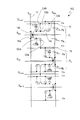
図1(a)および(b)を参照して、本発明による実施形態の液晶表示装置100の構造を説明する。図1(a)は液晶表示装置100の模式的な平面図であり、図1(b)は液晶表示パネル10における画素の電気的な接続関係を示す模式図である。
With reference to FIGS. 1A and 1B, the structure of a liquid
図1(a)に示すように、液晶表示装置100は、複数の行および複数の列を含むマトリクス状に配列された複数の画素Pを有する液晶表示パネル10と、液晶表示パネル10に駆動信号を供給する走査線駆動回路(ゲートドライバ)20および信号線駆動回路(ソースドライバ)30とを備える。
As shown in FIG. 1A, a liquid
液晶表示パネル10の複数の画素Pは、複数のカラー表示画素PCDを構成しており、カラー表示画素PCDのそれぞれは、4つの画素Pを含んでおり、4つの画素Pは、2行2列に配列された第1画素P1、第2画素P2、第3画素P3および第4画素P4である。ここで、第1画素P1と第2画素P2および第3画素P3と第4画素P4がそれぞれ行方向に沿って隣接し、且つ、第1画素P1と第3画素P3および第2画素P2と第4画素P4がそれぞれ列方向に沿って隣接して配列されている。The plurality of pixels P of the liquid
ここでは、第1画素P1が赤(R)画素、第2画素P2が黄(Y)画素、第3画素P3が青(B)画素、第4画素P4が緑(G)画素の例を示している。なお、図1(a)ではカラー表示画素の1行1列分だけを図示し、他を省略しているが、全て同じカラー表示画素がマトリクス状に配列されている。なお、カラー表示画素を構成する4つの画素P1〜P4の色は、この例に限られない。色再現性の観点から、少なくともR、GおよびB画素を含んでいることが好ましく、他の1つの色は、黄(Y)の他、シアン(C)またはマゼンタ(M)であることが好ましいが、白(W)であってもよい。Here, the first pixel P 1 is a red (R) pixel, the second pixel P 2 is a yellow (Y) pixel, the third pixel P 3 is a blue (B) pixel, and the fourth pixel P 4 is a green (G) pixel. An example is shown. In FIG. 1A, only one row and one column of color display pixels are shown and the others are omitted, but the same color display pixels are all arranged in a matrix. Note that the colors of the four pixels P 1 to P 4 constituting the color display pixel are not limited to this example. From the viewpoint of color reproducibility, it is preferable that at least R, G, and B pixels are included, and the other one color is preferably cyan (C) or magenta (M) in addition to yellow (Y). May be white (W).
なお、4つの画素P1〜P4の大きさは全て等しい必要はない。色再現性の観点から赤画素および青画素が他の2色の画素よりも大きいことが好ましい。このとき、走査線および信号線を直線的に配置できるように、各画素の形状は略矩形で、行方向に配列される第1画素P1と第2画素P2、および第3画素P3と第4画素P4の列方向の長さはそれぞれ互いに等しいことが好ましく、列方向に配列される第1画素P1と第3画素P3、および第2画素P2と第4画素P4の行方向の長さ(幅)はそれぞれ互いに等しいことが好ましい。また、カラー表示画素PCDは概ね正方形であることが好ましい。Note that the sizes of the four pixels P 1 to P 4 need not all be equal. From the viewpoint of color reproducibility, it is preferable that the red pixel and the blue pixel are larger than the other two-color pixels. At this time, the shape of each pixel is substantially rectangular so that the scanning line and the signal line can be arranged linearly, and the first pixel P 1 , the second pixel P 2 , and the third pixel P 3 arranged in the row direction. The fourth pixel P 4 and the fourth pixel P 4 are preferably equal in length in the column direction. The first pixel P 1 and the third pixel P 3 , and the second pixel P 2 and the fourth pixel P 4 are arranged in the column direction. The lengths (widths) in the row direction are preferably equal to each other. Further, it is preferable that the color display pixel P CD is approximately square.
次に、図1(b)を参照して、液晶表示パネル10における画素の電気的な接続関係を説明する。図1(b)は、液晶表示パネル10が有するアクティブマトリクス基板(TFT基板)10aの平面図を示しており、液晶層および液晶層を介してアクティブマトリクス基板10aに対向するように配置される対向基板の図示は省略している。対向基板は、典型的には、対向電極、カラーフィルタ層、遮光層(ブラックマトリクス)などが形成されている。なお、カラーフィルタ層はアクティブマトリクス基板に形成されてもよい。また、良く知られているように、IPSモードやFFSモードの液晶表示パネルにおいては、対向電極もアクティブマトリクス基板に形成され得る。
Next, with reference to FIG. 1B, an electrical connection relationship of pixels in the liquid
図1(b)は、アクティブマトリクス基板10aの、1つのカラー表示画素PCDを構成する4個の画素に対応する領域を示している。FIG. 1 (b) shows areas corresponding to the four pixels constituting the
図1(b)に示すように、アクティブマトリクス基板10aは、画素Pのそれぞれに設けられた画素電極11、画素電極11に接続されたスイッチング素子(ここではTFT)14、行方向に延びる複数の走査線(ゲートバスライン)12および列方向に延びる複数の信号線(ソースバスライン)13を有する。図1(a)に示した走査線駆動回路20は、複数の走査線12のそれぞれに走査信号を供給し、信号線駆動回路30は、複数の信号線13のそれぞれに正または負の信号電圧を供給する。ここでは、スイッチング素子としてTFT14を備えるTFT型の液晶表示装置について説明するが、スイッチング素子は、TFT14と同様の動作を行うものであれば、これに限られない。
As shown in FIG. 1B, the
複数の信号線13は、各画素列に対応して配置された第1信号線13aおよび第2信号線13bを含んでいる。第1信号線13aおよび第2信号線13bは、各垂直走査期間において、信号線駆動回路30から互いに逆の極性の信号電圧が供給される。例えば、第1信号線13aに正の信号電圧が供給されているときには、第2信号線13bには負の信号電圧が供給されている。ここでは、各画素列に対応して配置された2本の信号線13a、13bのうち左側に配置されている信号線を第1信号線13a、右側の信号線を第2信号線13bとそれぞれ呼び、第1信号線13aおよび第2信号線13bに供給される信号電圧の極性は、画素列ごとに独立である。すなわち、図1(b)において、n番目の画素列に対応して配置された第1信号線Sa(n)に供給される信号電圧の極性と、n+1番目の画素列に対応して配置された第1信号線Sa(n+1)に供給される信号電圧の極性とは互いに独立であり、同様に、n番目の画素列に対応して配置された第2信号線Sb(n)に供給される信号電圧の極性と、n+1番目の画素列に対応して配置された第2信号線Sb(n+1)に供給される信号電圧の極性とは互いに独立である。いずれの場合も、第1信号線Sa(n)に供給される信号電圧の極性と、第2信号線Sb(n)に供給される信号電圧の極性とは互いに逆であり、第1信号線Sa(n+1)に供給される信号電圧の極性と、第2信号線Sb(n+1)に供給される信号電圧の極性とは互いに逆である。The plurality of
任意のカラー表示画素PCDにおいて、第1画素P1および第3画素P3の一方のTFT14は第1信号線13aに接続されており、他方のTFT14は第2信号線13bに接続されている。また、第2画素P2および第4画素P4の一方のTFT14は第1信号線13aに接続されており、他方のTFT14は第2信号線13bに接続されている。ここでは、第1画素P1のTFT14は第1信号線13aに接続されており、第3画素P3のTFT14は第2信号線13bに接続されている。また、第2画素P2のTFT14は第2信号線13bに接続されており、第4画素P4のTFT14は第1信号線13aに接続されているが、それぞれ逆の信号線13に接続されていてもよい。In any color display pixel P CD, one of TFT14 of the first pixel P 1 and the third pixel P 3 is connected to the
ここで、4つの画素P1〜P4のTFT14は全て、共通の走査信号によってオン/オフ制御される。ここでは、4つの画素P1〜P4のTFT14は全て、共通の走査線12に接続されているが、共通の走査信号によってオン/オフ制御される限り、異なる走査線から走査信号が供給されてもよい。例えば、後述するように、1つの画素電極を2つの副画素電極で構成することによって、1つの画素を、表示すべき中間調よりも高い輝度を呈する明副画素と、表示すべき中間調よりも低い輝度を呈する暗副画素で構成する場合、2つの副画素電極に対応して、2本の走査線を設けて、各走査線に共通の走査信号を供給する。Here, all the
このように構成すると、1つのカラー表示画素PCDに含まれる4つの画素P1〜P4は1本の走査線G(m)と、4本の信号線Sa(n)、Sb(n)、Sa(n+1)およびSb(n+1)によって駆動されるので、従来のストライプ配列(各行に4つの色画素を配列し、各列はいずれか1色の画素が配列される)よりも画素行の数が増えた(2倍)にも拘わらず、各画素に信号電圧を供給する時間(TFT14をオンする時間、「書き込み時間」ということもある)を、従来のストライプ配列のときと同じにできる。従って、走査信号線の駆動に関しては、2倍速駆動や4倍速駆動を行うのに障害はない。With this configuration, the four pixels P 1 to P 4 included in one color display pixel P CD are each composed of one scanning line G (m) and four signal lines S a (n) , S b ( n) Since it is driven by S a (n + 1) and S b (n + 1) , a conventional stripe arrangement (4 color pixels are arranged in each row, and one color pixel is arranged in each column) The time for supplying a signal voltage to each pixel (the time for turning on the
さらに、第1画素P1に印加される電圧と第3画素P3に印加される電圧の極性は互いに逆で、且つ、第2画素P2に印加される電圧と第4画素P4に印加される電圧の極性は互いに逆であるので、各カラー表示画素PCDに含まれる4つの画素P1〜P4の2つに正の電圧が印加され、他の2つには負の電圧が印加される。Further, the polarity of the voltage applied to the first pixel P 1 and the voltage applied to the third pixel P 3 are opposite to each other, and the voltage applied to the second pixel P 2 and the voltage applied to the fourth pixel P 4 are reversed. since the polarity of the voltage is opposite to each other, each of the positive voltage to the two color
さらに、本発明による実施形態の液晶表示装置100では、任意の垂直走査期間において、第1信号線13aおよび第2信号線13bに供給される信号電圧の極性は一定である。もちろん、液晶表示装置100においても、交流駆動を行うので、垂直走査期間ごとに、第1信号線13aおよび第2信号線13bに供給される信号電圧の極性は反転される。すなわち、信号線駆動回路30は、画素行の数に拘わらず、垂直走査期間ごとに、各信号線13に供給する信号電圧の極性を反転するだけである(すなわち、極性反転の周期は、垂直走査期間の2倍となる)。従って、液晶表示装置100の信号線駆動回路30の負荷は、特許文献1、2に記載された液晶表示装置や、従来の一般的なストライプ配列の液晶表示装置における信号線駆動回路の負荷よりも小さい。ここでは、各信号線13に供給する信号電圧の極性を垂直走査期間ごとに反転させる例を説明するが、各信号線13に供給する信号電圧の極性を2以上の垂直走査期間ごとに反転させてもよい。例えば、240Hz駆動するときに、同じ画像を2垂直走査期間に亘って同じ極性で書き込むと、画素への充電時間を十分に確保できるという利点が得られる。また、極性反転の周期が長いほど、消費電力が低減される。
Furthermore, in the liquid
液晶表示装置100が有する上記の利点は、2倍速や4倍速駆動を行った場合、すなわち、垂直走査期間が1/120秒以下の場合に顕著であるが、従来の60Hz駆動においても、消費電力を低減できるという利点が得られる。従って、特許文献1、2に記載されているように、フリッカの発生を防止するように構成することが好ましい。以下、図2〜図5を参照して、フリッカの発生を防止するための構成を説明する。
The above-mentioned advantage of the liquid
図2〜5は、液晶表示装置100の液晶表示パネル10として用いられる液晶表示パネル10A〜10Dにおける、4つの画素P1〜P4のTFT14と2本の信号線13との接続関係および画素に印加される信号電圧の極性の分布を示す図である。2 to 5 show the connection relationship between the
図2〜5に示す液晶表示パネル10A〜10Dはいずれも、図1を参照して説明した液晶表示パネル10の構成を備えており、各信号線13に供給される信号電圧の極性は垂直走査期間内には変化せず、垂直走査期間ごとに反転される。図2〜5に示す画素に印加されている電圧の極性は、ある垂直走査期間における極性を示しており、次の垂直走査期間で全ての画素の極性が反転する。
Each of the liquid
図2および図3に示す液晶表示パネル10A、10Bでは、4本の信号線Sa(n)、Sb(n)、Sa(n+1)およびSb(n+1)の内、信号線Sa(n)とSa(n+1)とが同極性(ここでは正)で、信号線Sb(n)とSb(n+1)とが同極性(ここでは負)である。一方、図4および図5に示す液晶表示パネル10C、10Dでは、4本の信号線Sa(n)、Sb(n)、Sa(n+1)およびSb(n+1)の内、信号線Sa(n)とSb(n+1)とが同極性(ここでは正)で、信号線Sb(n)とSa(n+1)とが同極性(ここでは負)である。In the liquid
図2および図3に示すように、互いに隣接する任意の2本の信号線に供給される信号電圧の極性が逆であると、以下のような利点が得られる。例えば、信号線上に小さな異物があり、異物を介して、2本の信号線(例えばSb(n)およびSa(n+1))間に軽微なリーク電流が発生していた場合、近接する信号線に供給される電圧が逆極性であると、これらの信号線の間に比較的高い電圧が印加されることになるので、異物に比較的大きな電流が流れる。そうすると、そのジュール熱によって異物が破壊される結果、リーク不良が修復されることがある。また、隣接する信号線に供給される信号電圧の極性が互いに反対であると、従来のR、G、Bストライプ配列の液晶表示装置のドット反転駆動用の信号線駆動回路をそのまま利用することができる。As shown in FIGS. 2 and 3, when the polarities of the signal voltages supplied to any two adjacent signal lines are reversed, the following advantages are obtained. For example, if there is a small foreign object on the signal line and a slight leak current is generated between the two signal lines (for example, S b (n) and S a (n + 1) ) via the foreign object, If the voltage supplied to the signal lines to be reversed has a reverse polarity, a relatively high voltage is applied between these signal lines, so that a relatively large current flows through the foreign matter. As a result, the leakage failure may be repaired as a result of the destruction of foreign matter by the Joule heat. Further, if the polarities of the signal voltages supplied to the adjacent signal lines are opposite to each other, the signal line driving circuit for dot inversion driving of the conventional liquid crystal display device having R, G, B stripe arrangement can be used as it is. it can.
図2に示す液晶表示パネル10Aの、m行n列の第1画素P1を含むカラー表示画素PCDにおいては、第1画素P1のTFT14は第1信号線Sa(n)に接続されており、第3画素P3のTFT14は第2信号線Sb(n)に接続されている。また、第2画素P2のTFT14は第2信号線Sb(n+1)に接続されており、第4画素P4のTFT14は第1信号線Sa(n+1)に接続されている。従って、4つの画素P1〜P4のそれぞれに供給される信号電圧の極性は、第1画素P1と第2画素P2との間および第3画素P3と第4画素P4との間で互いに逆になっている。Of the liquid
次に、m+1行、n列の第1画素P1を含むカラー表示画素PCDに注目する。このカラー表示画素では、第1画素P1のTFT14は第2信号線Sb(n)に接続されており、第3画素P3のTFT14は第1信号線Sa(n)に接続されている。また、第2画素P2のTFT14は第1信号線Sa(n+1)に接続されており、第4画素P4のTFT14は第2信号線Sb(n+1)に接続されている。Next, m + 1 line, focus on color display pixel P CD including the first pixel P 1 of the n columns. In this color display pixel, the
すなわち、列方向に隣接する2つのカラー表示画素の間で、それぞれ対応する4つの画素P1〜P4のTFT14と2本の信号線13(例えば、信号線Sa(n)、Sb(n)および信号線Sa(n+1)、Sb(n+1))との接続関係は、互いに逆になっている。その結果、列方向に隣接する同じ色の画素に印加される電圧の極性は互いに逆になっている。例えば、m行n列の第1画素P1には正の電圧が印加され、m+1行n列の第1画素P1には負の電圧が印加される。他の第2〜第4画素についても同様に、列方向に隣接する2つのカラー表示画素間で、各色の画素に印加される電圧の極性は、互いに逆になっている。That is, between two color display pixels adjacent in the column direction, the corresponding
次に、m行n+2列の第1画素P1を含むカラー表示画素PCDに注目する。このカラー表示画素では、第1画素P1のTFT14は第2信号線Sb(n+2)に接続されており、第3画素P3のTFT14は第1信号線Sa(n+2)に接続されている。また、第2画素P2のTFT14は第1信号線Sa(n+3)に接続されており、第4画素P4のTFT14は第2信号線Sb(n+3)に接続されている。Next, attention is paid to the color display pixels P CD including the first pixel P 1 of m rows n + 2 rows. In this color display pixel, the
すなわち、行方向に隣接する2つのカラー表示画素の間で、それぞれ対応する4つの画素P1〜P4のTFT14と2本の信号線13(例えば、信号線Sa(n)、Sb(n)および信号線Sa(n+2)、Sb(n+2))との接続関係は、互いに逆になっている。その結果、行方向に隣接する同じ色の画素に印加される電圧の極性は互いに逆になっている。例えば、m行n列の第1画素P1には正の電圧が印加され、m行n+2列の第1画素P1には負の電圧が印加される。他の第2〜第4画素についても同様に、行方向に隣接する2つのカラー表示画素間で、各色の画素に印加される電圧の極性は、互いに逆になっている。That is, between the two color display pixels adjacent in the row direction, the corresponding
図2からわかるように、(ハッチングを付している)第1画素P1に印加される電圧は、列方向に隣接するカラー表示画素間で互いに逆であり、且つ、行方向に隣接するカラー表示画素間で互いに逆である。他の第2〜第4画素についても同様である。従って、液晶表示パネル10Aを用いても、特許文献1、2に記載の液晶表示装置と同様に、フリッカの発生が防止される。As can be seen from FIG. 2, the voltages applied to the first pixel P 1 (hatched) are opposite to each other between the color display pixels adjacent in the column direction and are adjacent to each other in the row direction. The display pixels are opposite to each other. The same applies to the other second to fourth pixels. Therefore, even when the liquid
次に図3を参照する。図3に示す液晶表示パネル10Bの、m行n列の第1画素P1を含むカラー表示画素PCDにおいては、第1画素P1のTFT14は第1信号線Sa(n)に接続されており、第3画素P3のTFT14は第2信号線Sb(n)に接続されている。また、第2画素P2のTFT14は第1信号線Sa(n+1)に接続されており、第4画素P4のTFT14は第2信号線Sb(n+1)に接続されている。第2画素P2および第4画素P4のTFT14と2本の信号線Sa(n+1)およびSb(n+1)との接続関係が、図2に示した液晶表示パネル10Aと逆になっている。従って、4つの画素P1〜P4のそれぞれに供給される信号電圧の極性は、第1画素P1と第2画素P2との間および第3画素P3と第4画素P4との間で互いに同じである。Reference is now made to FIG. Of the liquid
次に、m+1行、n列の第1画素P1を含むカラー表示画素PCDに注目する。このカラー表示画素では、第1画素P1のTFT14は第2信号線Sb(n)に接続されており、第3画素P3のTFT14は第1信号線Sa(n)に接続されている。また、第2画素P2のTFT14は第2信号線Sb(n+1)に接続されており、第4画素P4のTFT14は第1信号線Sa(n+1)に接続されている。Next, m + 1 line, focus on color display pixel P CD including the first pixel P 1 of the n columns. In this color display pixel, the
すなわち、列方向に隣接する2つのカラー表示画素の間で、それぞれ対応する4つの画素P1〜P4のTFT14と2本の信号線13(例えば、信号線Sa(n)、Sb(n)および信号線Sa(n+1)、Sb(n+1))との接続関係は、互いに逆になっている。その結果、列方向に隣接する同じ色の画素に印加される電圧の極性は互いに逆になっている。例えば、m行n列の第1画素P1には正の電圧が印加され、m+1行n列の第1画素P1には負の電圧が印加される。他の第2〜第4画素についても同様に、列方向に隣接する2つのカラー表示画素間で、各色の画素に印加される電圧の極性は、互いに逆になっている。That is, between two color display pixels adjacent in the column direction, the corresponding
次に、m行n+2列の第1画素P1を含むカラー表示画素PCDに注目する。このカラー表示画素では、第1画素P1のTFT14は第2信号線Sb(n+2)に接続されており、第3画素P3のTFT14は第1信号線Sa(n+2)に接続されている。また、第2画素P2のTFT14は第2信号線Sb(n+3)に接続されており、第4画素P4のTFT14は第1信号線Sa(n+3)に接続されている。Next, attention is paid to the color display pixels P CD including the first pixel P 1 of m rows n + 2 rows. In this color display pixel, the
すなわち、行方向に隣接する2つのカラー表示画素の間で、それぞれ対応する4つの画素P1〜P4のTFT14と2本の信号線13(例えば、信号線Sa(n)、Sb(n)および信号線Sa(n+2)、Sb(n+2))との接続関係は、互いに逆になっている。その結果、行方向に隣接する同じ色の画素に印加される電圧の極性は互いに逆になっている。例えば、m行n列の第1画素P1には正の電圧が印加され、m行n+2列の第1画素P1には負の電圧が印加される。他の第2〜第4画素についても同様に、行方向に隣接する2つのカラー表示画素間で、各色の画素に印加される電圧の極性は、互いに逆になっている。That is, between the two color display pixels adjacent in the row direction, the corresponding
図3からわかるように、(ハッチングを付している)第1画素P1に印加される電圧は、列方向に隣接するカラー表示画素間で互いに逆であり、且つ、行方向に隣接するカラー表示画素間で互いに逆である。他の第2〜第4画素についても同様である。従って、液晶表示パネル10Bを用いても、特許文献1、2に記載の液晶表示装置と同様に、フリッカの発生が防止される。As can be seen from FIG. 3, the voltages applied to the first pixels P 1 (hatched) are opposite to each other between the color display pixels adjacent in the column direction and are adjacent to each other in the row direction. The display pixels are opposite to each other. The same applies to the other second to fourth pixels. Therefore, even when the liquid
次に図4を参照する。図4に示す液晶表示パネル10Cの、m行n列の第1画素P1を含むカラー表示画素PCDにおいては、第1画素P1のTFT14は第1信号線Sa(n)に接続されており、第3画素P3のTFT14は第2信号線Sb(n)に接続されている。また、第2画素P2のTFT14は第1信号線Sa(n+1)に接続されており、第4画素P4のTFT14は第2信号線Sb(n+1)に接続されている。Reference is now made to FIG. Of the liquid
液晶表示パネル10Cにおける4つの画素P1〜P4のTFT14と2本の信号線13との接続関係は、図3に示した液晶表示パネル10Bと同じである。液晶表示パネル10Cと液晶表示パネル10Bとの違いは、信号線13に供給される信号電圧の極性にある。すなわち、液晶表示パネル10Bにおいて、1つのカラー表示画素に対応する4本の信号線Sa(n)、Sb(n)、Sa(n+1)およびSb(n+1)の内、信号線Sa(n)とSa(n+1)とが同極性(ここでは正)で、信号線Sb(n)とSb(n+1)とが同極性(ここでは負)であったのに対し、液晶表示パネル10Cでは、4本の信号線Sa(n)、Sb(n)、Sa(n+1)およびSb(n+1)の内、信号線Sa(n)とSb(n+1)とが同極性(ここでは正)で、信号線Sb(n)とSa(n+1)とが同極性(ここでは負)である。The connection relationship between the
図4と図3とを比較すれば明らかなように、図3における第2画素P2および第4画素P4の極性を逆にすれば、図4の各画素の極性の分布と一致する。液晶表示装置10Cにおいては、4つの画素P1〜P4のそれぞれに供給される信号電圧の極性は、第1画素P1と第2画素P2との間および第3画素P3と第4画素P4との間で互いに逆になっている。As apparent from a comparison between FIG. 4 and FIG. 3, if the polarities of the second pixel P 2 and the fourth pixel P 4 in FIG. 3 are reversed, the distribution of the polarities of each pixel in FIG. In the liquid
図4からわかるように、(ハッチングを付している)第1画素P1に印加される電圧は、列方向に隣接するカラー表示画素間で互いに逆であり、且つ、行方向に隣接するカラー表示画素間で互いに逆である。他の第2〜第4画素についても同様である。従って、液晶表示パネル10Cを用いても、特許文献1、2に記載の液晶表示装置と同様に、フリッカの発生が防止される。As can be seen from FIG. 4, the voltages applied to the first pixels P 1 (hatched) are opposite to each other between the color display pixels adjacent in the column direction and are adjacent to each other in the row direction. The display pixels are opposite to each other. The same applies to the other second to fourth pixels. Therefore, even when the liquid
次に図5を参照する。図5に示す液晶表示パネル10Dの、m行n列の第1画素P1を含むカラー表示画素PCDにおいては、第1画素P1のTFT14は第1信号線Sa(n)に接続されており、第3画素P3のTFT14は第2信号線Sb(n)に接続されている。また、第2画素P2のTFT14は第2信号線Sb(n+1)に接続されており、第4画素P4のTFT14は第1信号線Sa(n+1)に接続されている。Reference is now made to FIG. Of the liquid
液晶表示パネル10Dにおける4つの画素P1〜P4のTFT14と2本の信号線13との接続関係は、図2に示した液晶表示パネル10Aと同じである。液晶表示パネル10Dと液晶表示パネル10Aとの違いは、信号線13に供給される信号電圧の極性にある。すなわち、液晶表示パネル10Aにおいて、1つのカラー表示画素に対応する4本の信号線Sa(n)、Sb(n)、Sa(n+1)およびSb(n+1)の内、信号線Sa(n)とSa(n+1)とが同極性(ここでは正)で、信号線Sb(n)とSb(n+1)とが同極性(ここでは負)であったのに対し、液晶表示パネル10Dでは、4本の信号線Sa(n)、Sb(n)、Sa(n+1)およびSb(n+1)の内、信号線Sa(n)とSb(n+1)とが同極性(ここでは正)で、信号線Sb(n)とSa(n+1)とが同極性(ここでは負)である。The connection relationship between the
図5と図2とを比較すれば明らかなように、図5における第2画素P2および第4画素P4の極性を逆にすれば、図2の各画素の極性の分布と一致する。液晶表示装置10Dにおいては、4つの画素P1〜P4のそれぞれに供給される信号電圧の極性は、第1画素P1と第2画素P2との間および第3画素P3と第4画素P4との間で互いに同じである。As apparent from a comparison between FIG. 5 and FIG. 2, if the polarities of the second pixel P 2 and the fourth pixel P 4 in FIG. 5 are reversed, the distribution of the polarities of the respective pixels in FIG. In the liquid
図5からわかるように、(ハッチングを付している)第1画素P1に印加される電圧は、列方向に隣接するカラー表示画素間で互いに逆であり、且つ、行方向に隣接するカラー表示画素間で互いに逆である。他の第2〜第4画素についても同様である。従って、液晶表示パネル10Dを用いても、特許文献1、2に記載の液晶表示装置と同様に、フリッカの発生が防止される。As can be seen from FIG. 5, the voltages applied to the first pixels P 1 (hatched) are opposite to each other between the color display pixels adjacent in the column direction and are adjacent to each other in the row direction. The display pixels are opposite to each other. The same applies to the other second to fourth pixels. Therefore, even when the liquid
次に、図6および図7を参照して、マルチ画素構造を有する液晶表示パネル10Eの構造と動作を説明する。マルチ画素構造とは、個々の画素が、ある中間調を表示するときに、表示すべき中間調よりも高い輝度を呈する明副画素と、表示すべき中間調よりも低い輝度を呈する暗副画素を有する構造を言う。マルチ画素構造を導入することによって、γ特性の視角依存性を改善することができる。マルチ画素構造として、例えば特開2006−133577号公報に記載されている構造を採用することができる。参考のために、特開2006−133577号公報の開示内容の全てを本明細書に援用する。
Next, the structure and operation of the liquid
図6は、液晶表示パネル10Eにおける画素のTFTと信号線との接続関係とともに、走査信号としてのゲート信号がオンとなるタイミングを併せて示している。図7は、図6中の一点鎖線で囲んだ3画素の等価回路を示す図である。
FIG. 6 shows the connection relationship between the pixel TFT and the signal line in the liquid
図6の液晶表示パネル10Eは、図2の液晶表示パネル10Aにマルチ画素構造を適用したものであり、4つの画素P1〜P4のそれぞれが副画素Paと副画素Pbとを有している。ここでは、副画素Paが明副画素、副画素Pbが暗副画素となる例を示す。明副画素Paと暗副画素Pbは、各画素を列方向に2分割して形成されている。ここでは、簡単のために、明副画素Paと暗副画素Pbの面積は互いにほぼ等しく図示しているが、副画素Paと副画素Pbとの面積比はこれに限られず、適宜変更され得る。なお、カラー表示画素PCDを構成する4つの画素P1〜P4の明副画素Paは、ここで例示するように、カラー表示画素PCDの列方向の中心に配置されることが好ましい。すなわち、第1画素P1および第2画素P2の下側の副画素および第3画素P3および第4画素P4の上側の副画素を明副画素Paとすることが好ましい。A liquid
第1、第2画素の明副画素と、第3、第4画素の明副画素との間に暗副画素が存在すると、色のにじみが発生することがある。例えば、画素行に平行なエッジを有する白い四角形を表示したとき、四角形の上端のエッジでは、エッジに対応する画素行の第1および第2画素の明副画素が目立つ。すなわち、2色の画素の明副画素が目立つので、白い四角形の上端のエッジに色がにじんだ様に見えることになる。上述したように、カラー表示画素PCDを構成する4つの画素P1〜P4の明副画素Paをカラー表示画素PCDの列方向の中心に配置すると、4つの色の明副画素Paが近接するので、色のにじみを防止することができる。If dark subpixels exist between the bright subpixels of the first and second pixels and the bright subpixels of the third and fourth pixels, color blur may occur. For example, when a white square having an edge parallel to the pixel row is displayed, the bright subpixels of the first and second pixels in the pixel row corresponding to the edge are conspicuous at the upper edge of the square. That is, since the bright subpixels of the two color pixels are conspicuous, the color appears to blur at the upper edge of the white square. As described above, placing the bright subpixel Pa of the four pixels P 1 to P 4 constituting the color display pixel P CD in the column direction of the center of the color display pixel P CD, four colors of bright pixel Pa is Since they are close to each other, color bleeding can be prevented.
図6に示すように、4つの画素P1〜P4はそれぞれ、明副画素Paおよび暗副画素Pbを有している。明副画素PaはTFT14aに接続されており、暗副画素PbはTFT14bに接続されている。TFT14aおよび14bのゲートは共通の走査線12に接続されており、TFT14aおよび14bのソースは共通の信号線13に接続されている。すなわち、副画素Pa、Pbはそれぞれ、図1(b)に示した画素電極11に対応する副画素電極を有し、副画素Pa、Pbの副画素電極は、それぞれ対応するTFT14a、14bのドレインに接続されており、TFT14a、14bを介して共通の信号線(ソースバスライン)13に接続されている。As shown in FIG. 6, each of the four pixels P 1 to P 4 has a bright sub-pixel Pa and a dark sub-pixel Pb. The bright subpixel Pa is connected to the
図2に示した液晶表示パネル10Aでは、第1画素P1および第3画素P3と、第2画素P2および第4画素P4の合計4個のTFT14が共通の走査線(ゲートバスライン)12に接続されていたのに対し、液晶表示パネル10Eでは、第1画素P1の明副画素および暗副画素と、第2画素P2の明副画素および暗副画素の合計4個のTFT14a、14bが共通の走査線12(例えば図6中の上側のG(m))に接続されている。また、同様に、第3画素P3の明副画素および暗副画素と、第4画素P4の明副画素および暗副画素の合計4個のTFT14a、14bが共通の他の走査線12(例えば図6中の下側のG(m))に接続されている。図6に示すように、これら2本の走査線12には、共通のゲート信号が供給される。図6に示したゲート信号がハイになる期間に、TFT14a、14bがオン状態になり、対応する信号線13から信号電圧が供給される。従って、液晶表示パネル10Eの4つの画素P1〜P4の各副画素(合計8個の副画素)には、対応するTFT14a、14bがオン状態になったときに、(液晶表示パネル10Aの4つの画素P1〜P4と同様に、)対応する信号電圧が供給される。TFT14a、14bのゲートは、共通のゲート信号によってオン/オフ制御される。In the liquid
液晶表示パネル10Eの4つの画素P1〜P4のそれぞれは、さらに第3のTFT14cを有している。TFT14cは、図7に示すように、暗副画素Pbの容量CSbに対して並列に接続されたバッファ容量CScとの間の電気的な接続をスイッチングする。このTFT14cのゲートは、次段の走査線(例えば、(G(m+1))に接続されており、次段、すなわち列方向に隣接するカラー表示画素のTFT14a、14bと同じタイミングでオン状態となる。この第3のTFT14cをオン状態とすることによって、副画素Pbが暗副画素となる。Each of the four pixels P 1 to P 4 of the liquid
図7を参照して、液晶表示パネル10Eのm行n列の第1画素P1に明副画素Paと暗副画素Pbとが形成される動作を説明する。Referring to FIG 7, the operation of the first pixel P 1 of m rows and n columns of the liquid
走査線G(m)のゲート信号がハイになると、TFT14a、14bがオン状態となり、信号線Sa(n)から、所定の信号電圧(V(k)とする。)が副画素Pa、Pbに供給され、副画素Paの液晶容量Clcaおよび補助容量CSa(副画素容量CPaともいう。)、副画素Pbの液晶容量Clcbおよび補助容量CSb(副画素容量CPbともいう。)が充電される。液晶容量Clca、Clcbを構成する一方の電極は各副画素の副画素電極であり、他方の電極が対向電極である。対向電極には、共通電圧(対向電圧)COMが供給されている。補助容量CSa、CSbを構成する一方の電極は補助容量電極であり、TFT14aまたは14bのドレイン電極に接続されており、それぞれの副画素の副画素電極と同じ電圧が供給される。補助容量CSa、CSbを構成する他方の電極は補助容量配線(Cs)15に接続されており、補助容量電圧が供給される。When the gate signal of the scanning line G (m) becomes high, the
このとき、走査線G(m+1)のゲート信号はローなので、TFT14cはオフ状態にあり、バッファ容量CScは、前の垂直走査期間に書き込まれた信号電圧(V(k-1)とする。)が保持されている。ここで、液晶表示パネル10Eは、フレーム反転駆動されるので、現垂直走査期間に書き込まれる電圧の極性は、前垂直走査期間に書き込まれた電圧の極性と逆である。At this time, since the gate signal of the scanning line G (m + 1) is low, the
次に、走査線G(m)のゲート信号がローになり、TFT14a、14bがオフ状態になると、副画素容量CPaおよび副画素容量CPbはそれぞれ、V(k)を保持した状態になる。Next, when the gate signal of the scanning line G (m) becomes low and the
続いて、走査線G(m+1)のゲート信号がハイになると、TFT14cがオン状態になる。TFT14cがオン状態になると、副画素容量CPbと、バッファ容量CScとが並列に接続される。従って、副画素容量CPbが保持している電圧V(k)と、バッファ容量CScが保持している電圧V(k-1)とが等しくなるように、副画素容量CPbに蓄えられる電荷とバッファ容量CScに蓄えられる電荷が再分配されることになる。このとき、V(k-1)はV(k)と逆の極性を有しているので、副画素容量CPbとバッファ容量CScとに蓄積される全体の電荷量は減少し、副画素容量CPbの電圧はV(k)よりも小さくなる(絶対値が小さくなる)。その結果、副画素Pbの輝度は、電圧V(k)が保持されて状態を維持している副画素Paの輝度よりも低くなる。Subsequently, when the gate signal of the scanning line G (m + 1) becomes high, the
なお、各信号線に供給する信号電圧の極性を2以上の垂直走査期間ごとに反転させる場合でも、上記の動作によって、副画素Pbを暗副画素にすることができる。例えば、負の信号電圧を印加した後、極性を反転させて正の信号電圧を書き込むと、上述のように副画素Pbの輝度は副画素Paの輝度よりも低くなる。この後、さらに続けて正の同じ信号電圧を供給すると、このときの副画素Pbの輝度は変化しない。しかしながら、正の信号電圧を供給する2垂直走査期間の平均の輝度を考えると、副画素Pbの平均輝度は、副画素Paの輝度よりも低い。従って、各信号線に供給する信号電圧の極性を2以上の垂直走査期間ごとに反転させても、マルチ画素構造による効果を得ることができる。 Even when the polarity of the signal voltage supplied to each signal line is inverted every two or more vertical scanning periods, the subpixel Pb can be made a dark subpixel by the above operation. For example, when a negative signal voltage is applied and then the polarity is inverted and a positive signal voltage is written, the luminance of the sub-pixel Pb becomes lower than the luminance of the sub-pixel Pa as described above. Thereafter, when the same positive signal voltage is continuously supplied, the luminance of the sub-pixel Pb at this time does not change. However, considering the average luminance of two vertical scanning periods for supplying a positive signal voltage, the average luminance of the subpixel Pb is lower than the luminance of the subpixel Pa. Therefore, the effect of the multi-pixel structure can be obtained even if the polarity of the signal voltage supplied to each signal line is inverted every two or more vertical scanning periods.
特開2006−133577号公報に記載のマルチ画素構造は、1つの画素に複数の液晶ドメイン(典型的には少なくとも液晶層に電圧を印加したときに、液晶ドメインのディレクタの方位角(右方向、時計の文字盤の3時方向を0°とし、反時計回りを正とする)が、45°、135°、225°、315°となる4つの液晶ドメインを含む)が形成される、ノーマリーブラックモードで表示を行う垂直配向型の液晶表示装置に好適に用いられる。 The multi-pixel structure described in Japanese Patent Application Laid-Open No. 2006-133777 has a plurality of liquid crystal domains (typically, when a voltage is applied to at least a liquid crystal layer, a director azimuth (right direction, The clock face dial is 3 ° and the counterclockwise direction is positive (including four liquid crystal domains of 45 °, 135 °, 225 °, and 315 °). It is suitably used for a vertical alignment type liquid crystal display device that performs display in a black mode.
本発明の液晶表示装置に適用できる他のマルチ画素構造として、本出願人による特開2004−62146号公報(米国特許第6958791号明細書)に開示されているものを挙げることができる。このマルチ画素構造は、1つの画素内の複数の副画素ごとに補助容量を設け、補助容量を構成する補助容量対向電極(CSバスラインに接続されている)を副画素ごとに電気的に独立とし、補助容量対向電極に供給する電圧(補助容量対向電圧という。)を変化させることによって、容量分割を利用して、複数の副画素の液晶層に印加される実効電圧を異ならせる液晶表示装置が開示されている。特開2004−62146号公報(米国特許第6958791号明細書)の開示内容の全てを参考のために本明細書に援用する。 Other multi-pixel structures applicable to the liquid crystal display device of the present invention include those disclosed in Japanese Patent Application Laid-Open No. 2004-62146 (US Pat. No. 6,958,791) by the present applicant. In this multi-pixel structure, an auxiliary capacitor is provided for each of a plurality of subpixels in one pixel, and an auxiliary capacitor counter electrode (connected to the CS bus line) constituting the auxiliary capacitor is electrically independent for each subpixel. A liquid crystal display device that varies the effective voltage applied to the liquid crystal layers of the plurality of sub-pixels by changing the voltage supplied to the auxiliary capacitor counter electrode (referred to as an auxiliary capacitor counter voltage). Is disclosed. The entire disclosure of Japanese Patent Application Laid-Open No. 2004-62146 (US Pat. No. 6,958,791) is incorporated herein by reference.
特開2006−133577号公報には、垂直配向型の表示装置として、いわゆるMVAモードの液晶表示装置が記載されている。MVAモードの液晶表示装置は、電極に形成された直線状のスリットや電極の液晶層側に形成された直線状の誘電体突起(リブ)を、液晶層を介して対向する一対の基板に、基板の法線方向から見たときに、平行且つ交互になるように配置することによって、電圧印加時に形成される液晶ドメインのディレクタの方位を規制する。液晶ドメインの方位は、直線状のスリット又は誘電体突起(これらを総称して「直線状構造体」ということにする。)の延びる方位に直交する方向になる。 Japanese Patent Laid-Open No. 2006-133577 describes a so-called MVA mode liquid crystal display device as a vertical alignment type display device. The MVA mode liquid crystal display device has a linear slit formed on the electrode and a linear dielectric protrusion (rib) formed on the liquid crystal layer side of the electrode on a pair of substrates opposed via the liquid crystal layer. When viewed from the normal direction of the substrate, the directors of the liquid crystal domain formed at the time of voltage application are regulated by arranging them in parallel and alternately. The direction of the liquid crystal domain is a direction orthogonal to the direction in which the linear slits or dielectric protrusions (collectively referred to as “linear structures”) extend.
MVAモードの液晶表示装置は、現在液晶テレビに広く用いられている。しかしながら、MVAモードの液晶表示装置においては、直線状構造体からの配向規制力で、液晶ドメインのディレクタの方位を規制するので、直線状構造体の近傍の液晶分子の応答は速く(配向方向の変化が速く)、直線状構造体から離れた位置の液晶分子の応答が遅いという問題がある。 MVA mode liquid crystal display devices are currently widely used in liquid crystal televisions. However, in the MVA mode liquid crystal display device, the orientation of the director of the liquid crystal domain is regulated by the alignment regulating force from the linear structure, so that the response of the liquid crystal molecules in the vicinity of the linear structure is fast (the alignment direction There is a problem that the response of the liquid crystal molecules at a position away from the linear structure is slow.
MVAモードの液晶表示装置よりも応答特性に優れた垂直配向型の液晶表示装置として、PSAモードの液晶表示装置が知られている。Polymer Sustained Alignment Technology(以下、「PSA技術」という)は、例えば、特開2002−357830号公報、特開2003−177418号公報、特開2006−78968号公報、K. Hanaoka et al. "A New MVA-LCD by Polymer Sustained Alignment Technology", SID 04 DIGEST p.1200-1203(2004)、に開示されている。これら4つの文献の開示内容の全てを参考のために本明細書に援用する。 A PSA mode liquid crystal display device is known as a vertical alignment type liquid crystal display device having better response characteristics than an MVA mode liquid crystal display device. Polymer Sustained Alignment Technology (hereinafter referred to as “PSA technology”) is disclosed in, for example, JP 2002-357830 A, JP 2003-177418 A, JP 2006-78968 A, K. Hanaoka et al. “A New MVA-LCD by Polymer Sustained Alignment Technology ", SID 04 DIGEST p.1200-1203 (2004). The entire disclosure of these four documents is hereby incorporated by reference.
PSA技術は、液晶材料中に少量の重合性化合物(例えば光重合性モノマまたはオリゴマ)を混入しておき、液晶セルを組み立てた後、液晶層に所定の電圧を印加した状態で重合性材料に活性エネルギー線(例えば紫外線)を照射し、生成される重合体によって、液晶分子のプレチルト方向を制御する技術である。重合体が生成されるときの液晶分子の配向状態が、電圧を取り去った後(電圧を印加しない状態)においても維持(記憶)される。重合体で形成される層を、ここでは配向維持層ということにする。配向維持層は、配向膜の表面(液晶層側)に形成されるが、配向膜の表面を覆う膜の形態をとる必要は必ずしも無く、重合体の粒子が離散的に存在する形態もある。 In the PSA technology, a small amount of a polymerizable compound (for example, a photopolymerizable monomer or oligomer) is mixed in a liquid crystal material, and after assembling a liquid crystal cell, a predetermined voltage is applied to the liquid crystal layer. This is a technique of irradiating active energy rays (for example, ultraviolet rays) and controlling the pretilt direction of liquid crystal molecules by the polymer produced. The alignment state of the liquid crystal molecules when the polymer is generated is maintained (stored) even after the voltage is removed (a state where no voltage is applied). Here, the layer formed of the polymer is referred to as an orientation maintaining layer. The alignment sustaining layer is formed on the surface of the alignment film (on the liquid crystal layer side), but it is not always necessary to take the form of a film covering the surface of the alignment film, and there is a form in which polymer particles exist discretely.
PSA技術は、液晶層に形成される電界等を制御することによって、液晶分子のプレチルト方位およびプレチルト角度を調整することができるという利点を有している。また、配向維持層によって、液晶層に接するほぼ全ての面で配向規制力を発現するので、MVAモードの液晶表示装置よりも応答特性に優れるという特徴を有している。本発明は、特に2倍速駆動等を行う場合、PSAモードの液晶表示装置に適用することが好ましい。 The PSA technique has an advantage that the pretilt azimuth and pretilt angle of liquid crystal molecules can be adjusted by controlling the electric field formed in the liquid crystal layer. In addition, since the alignment maintaining layer exhibits an alignment regulating force on almost all surfaces in contact with the liquid crystal layer, the alignment maintaining layer has a characteristic that the response characteristic is superior to that of the MVA mode liquid crystal display device. The present invention is preferably applied to a PSA mode liquid crystal display device, particularly when double speed driving or the like is performed.
本発明による実施形態のPSAモードの液晶表示装置は、例えば、液晶表示パネル10の画素電極11として、図8に示す画素電極11Aを用い、上述のPSA技術を適用することによって得られる。
The PSA mode liquid crystal display device according to the embodiment of the present invention can be obtained, for example, by using the
画素電極11Aは、一対の偏光板の偏光軸と重なるように配置された十字形状の幹部11t1、11t2と、十字形状の幹部11t1、11t2から略45°方向に延びる複数の枝部11b1、11b2、11b3、および11b4とを有している。
The
幹部は、行方向(水平方向)に延びる幹部11t1と、列方向(垂直方向)に延びる幹部11t2とを有している。複数の枝部は、表示面の右方向(時計の文字盤の3時方向)の方位角を0°とすると、幹部から45°方位に延びる第1群(枝部11b1)と、135°方位に延びる第2群(枝部11b2)と、225°方位に延びる第3群(枝部11b3)と、315°方位に延びる第4群(枝部11b4)とを有している。垂直配向型の液晶層の液晶分子(誘電異方性が負)は、幹部および枝部からの斜め電界により、それぞれの枝部が延びる方位に傾斜する。これは、互いに平行に延びる枝部からの斜め電界は枝部が延びる方向に垂直な方位に液晶分子を傾斜させるように作用し、幹部からの斜め電界はそれぞれの枝部の延びる方位に液晶分子を傾斜させるように作用するからである。PSA技術を用いると、液晶層に電圧を印加した際に形成される、液晶分子の上記の配向を安定化させることができる。 The trunk includes a trunk 11t1 extending in the row direction (horizontal direction) and a trunk 11t2 extending in the column direction (vertical direction). When the azimuth angle in the right direction of the display surface (3 o'clock direction of the clock face) is 0 °, the plurality of branch portions and the first group (branch portion 11b1) extending in the 45 ° azimuth direction from the trunk portion and the 135 ° azimuth direction A second group (branches 11b2) extending in the direction of 225 °, a third group (branches 11b3) extending in the direction of 225 °, and a fourth group (branches 11b4) extending in the direction of 315 °. The liquid crystal molecules (with negative dielectric anisotropy) in the vertical alignment type liquid crystal layer are inclined in the direction in which each branch extends by an oblique electric field from the trunk and branches. This is because the oblique electric fields from the branches extending in parallel with each other act so that the liquid crystal molecules are tilted in the direction perpendicular to the direction in which the branches extend, and the oblique electric field from the trunk is in the direction in which each branch extends. This is because it acts so as to be inclined. When the PSA technique is used, the above-described alignment of liquid crystal molecules formed when a voltage is applied to the liquid crystal layer can be stabilized.
もちろん、本発明は、例示した実施形態の液晶表示装置に限られず、例えば、RTN(VATNともいう)モード、IPSモードやFSSモードの液晶表示装置に広く適用できる。 Of course, the present invention is not limited to the liquid crystal display device of the illustrated embodiment, and can be widely applied to, for example, liquid crystal display devices in an RTN (also referred to as VATN) mode, an IPS mode, or an FSS mode.
なお、上記の説明では、行方向を表示面の水平方向、列方向を垂直方向としたが、これは逆になってもよい。すなわち、ゲートバスラインを垂直方向に延びるように配置し、ソースバスラインを水平方向に延びるように配置してもよい。言い換えると、上記の説明における行方向と列方向とを入れ替えてもよい。 In the above description, the row direction is the horizontal direction of the display surface, and the column direction is the vertical direction, but this may be reversed. That is, the gate bus lines may be arranged to extend in the vertical direction, and the source bus lines may be arranged to extend in the horizontal direction. In other words, the row direction and the column direction in the above description may be interchanged.
本発明は、HDTV用の液晶表示装置をはじめ、液晶表示装置に広く用いられる。 The present invention is widely used in liquid crystal display devices including liquid crystal display devices for HDTV.
10、10A、10B、10C、10D、10E 液晶表示パネル
10a アクティブマトリクス基板
11 画素電極
12 走査線
13 信号線
13a 第1信号線
13b 第2信号線
14 薄膜トランジスタ(TFT)
15 補助容量配線
20 走査線駆動回路(ゲートドライバ)
30 信号線駆動回路(ソースドライバ)
100 液晶表示装置
P、P1、P2、P3、P4 画素
PCD カラー表示画素10, 10A, 10B, 10C, 10D, 10E Liquid
15
30 Signal line drive circuit (source driver)
100 Liquid crystal display devices P, P 1 , P 2 , P 3 , P 4 pixels P CD color display pixels
Claims (8)
前記複数の画素のそれぞれに設けられた画素電極、前記画素電極に接続されたスイッチング素子、行方向に延びる複数の走査線および列方向に延びる複数の信号線を有するアクティブマトリクス基板と、
前記アクティブマトリクス基板に対向する対向基板と、
前記アクティブマトリクス基板と前記対向基板との間に設けられた液晶層と、
前記複数の走査線のそれぞれに走査信号を供給する走査線駆動回路と、
前記複数の信号線のそれぞれに正または負の信号電圧を供給する信号線駆動回路と、
を備え、
前記複数の画素は、複数のカラー表示画素を構成しており、前記複数のカラー表示画素のそれぞれは、2行2列に配列された第1、第2、第3および第4画素であって、前記第1と第2画素および前記第3と第4画素がそれぞれ前記行方向に沿って隣接し、且つ、前記第1と第3画素および前記第2と第4画素がそれぞれ前記列方向に沿って隣接して配列された、第1、第2、第3および第4画素を含み、
前記第1、第2、第3および第4画素の色は、互いに異なり、前記複数のカラー表示画素のそれぞれにおいて、前記第1、第2、第3および第4画素は、同じパターンで配列され、
前記複数の信号線は、各画素列に対応して配置された第1および第2信号線であって、各垂直走査期間において、前記信号線駆動回路から互いに逆の極性の信号電圧が供給される第1信号線および第2信号線を含み、
任意のカラー表示画素において、前記第1および第3画素の一方の前記スイッチング素子は前記第1信号線に接続されており、他方の前記スイッチング素子は前記第2信号線に接続されており、前記第2および第4画素の一方の前記スイッチング素子は前記第1信号線に接続されており、他方のスイッチング素子は前記第2信号線に接続されており、かつ、前記第1、第2、第3および第4画素のスイッチング素子は全て、共通の走査信号によってオン/オフ制御され、
任意の垂直走査期間において、前記第1および第2信号線に供給される前記信号電圧の極性は一定であり、
任意の垂直走査期間において、任意のカラー表示画素に含まれる前記第1、第2、第3および第4画素のそれぞれに供給される前記信号電圧の極性と、前記任意のカラー表示画素に行方向に隣接するカラー表示画素に含まれる前記第1、第2、第3および第4画素のそれぞれに供給される前記信号電圧の極性とは、互いに逆である、液晶表示装置。 A liquid crystal display device having a plurality of pixels arranged in a matrix including a plurality of rows and a plurality of columns,
An active matrix substrate having a pixel electrode provided in each of the plurality of pixels, a switching element connected to the pixel electrode, a plurality of scanning lines extending in a row direction, and a plurality of signal lines extending in a column direction;
A counter substrate facing the active matrix substrate;
A liquid crystal layer provided between the active matrix substrate and the counter substrate;
A scanning line driving circuit for supplying a scanning signal to each of the plurality of scanning lines;
A signal line driving circuit for supplying a positive or negative signal voltage to each of the plurality of signal lines;
With
The plurality of pixels constitute a plurality of color display pixels, and each of the plurality of color display pixels is a first, second, third and fourth pixel arranged in two rows and two columns. The first and second pixels and the third and fourth pixels are adjacent to each other in the row direction, and the first and third pixels and the second and fourth pixels are respectively in the column direction. Comprising first, second, third and fourth pixels arranged adjacently along;
The colors of the first, second, third, and fourth pixels are different from each other, and the first, second, third, and fourth pixels are arranged in the same pattern in each of the plurality of color display pixels. ,
The plurality of signal lines are first and second signal lines arranged corresponding to each pixel column, and signal voltages having opposite polarities are supplied from the signal line driving circuit in each vertical scanning period. Including a first signal line and a second signal line,
In any color display pixel, one of the switching elements of the first and third pixels is connected to the first signal line, and the other switching element is connected to the second signal line, One of the switching elements of the second and fourth pixels is connected to the first signal line, the other switching element is connected to the second signal line, and the first, second, second All the switching elements of the third and fourth pixels are on / off controlled by a common scanning signal,
In any vertical scanning period, the polarity of the signal voltage supplied to the first and second signal lines Ri constant der,
In an arbitrary vertical scanning period, the polarity of the signal voltage supplied to each of the first, second, third, and fourth pixels included in an arbitrary color display pixel, and the row direction to the arbitrary color display pixel A liquid crystal display device , wherein polarities of the signal voltages supplied to the first, second, third, and fourth pixels included in the color display pixels adjacent to each other are opposite to each other .
Priority Applications (1)
| Application Number | Priority Date | Filing Date | Title |
|---|---|---|---|
| JP2011551896A JP5540020B2 (en) | 2010-01-29 | 2011-01-27 | Liquid crystal display |
Applications Claiming Priority (4)
| Application Number | Priority Date | Filing Date | Title |
|---|---|---|---|
| JP2010019258 | 2010-01-29 | ||
| JP2010019258 | 2010-01-29 | ||
| JP2011551896A JP5540020B2 (en) | 2010-01-29 | 2011-01-27 | Liquid crystal display |
| PCT/JP2011/051586 WO2011093374A1 (en) | 2010-01-29 | 2011-01-27 | Liquid crystal display device |
Publications (2)
| Publication Number | Publication Date |
|---|---|
| JPWO2011093374A1 JPWO2011093374A1 (en) | 2013-06-06 |
| JP5540020B2 true JP5540020B2 (en) | 2014-07-02 |
Family
ID=44319357
Family Applications (1)
| Application Number | Title | Priority Date | Filing Date |
|---|---|---|---|
| JP2011551896A Expired - Fee Related JP5540020B2 (en) | 2010-01-29 | 2011-01-27 | Liquid crystal display |
Country Status (5)
| Country | Link |
|---|---|
| US (1) | US9818348B2 (en) |
| EP (1) | EP2530513A4 (en) |
| JP (1) | JP5540020B2 (en) |
| CN (1) | CN102725676B (en) |
| WO (1) | WO2011093374A1 (en) |
Families Citing this family (16)
| Publication number | Priority date | Publication date | Assignee | Title |
|---|---|---|---|---|
| CN102750919A (en) * | 2012-06-26 | 2012-10-24 | 北京京东方光电科技有限公司 | Display panel as well as drive method and display device thereof |
| MY175398A (en) * | 2012-09-13 | 2020-06-24 | Sharp Kk | Liquid crystal display device |
| US9564095B2 (en) * | 2012-12-07 | 2017-02-07 | Sakai Display Products Corporation | Liquid crystal display device and method for driving the liquid crystal display device whereby shadowing can be prevented |
| KR102114818B1 (en) * | 2013-09-09 | 2020-05-26 | 삼성디스플레이 주식회사 | Display apparatus |
| US9697787B2 (en) * | 2013-09-09 | 2017-07-04 | Samsung Display Co., Ltd. | Display device |
| CN103792746A (en) | 2014-01-27 | 2014-05-14 | 北京京东方光电科技有限公司 | Array substrate, manufacturing method thereof and display device |
| JP2015165272A (en) * | 2014-03-03 | 2015-09-17 | 株式会社ジャパンディスプレイ | Display device and reflective liquid crystal display device |
| KR20160025146A (en) | 2014-08-26 | 2016-03-08 | 삼성디스플레이 주식회사 | Display apparatus |
| JP2016184097A (en) | 2015-03-26 | 2016-10-20 | 株式会社ジャパンディスプレイ | Display |
| CN107924662A (en) * | 2015-08-27 | 2018-04-17 | 堺显示器制品株式会社 | Liquid crystal display device |
| CN105954951B (en) * | 2016-07-08 | 2019-03-22 | 深圳市华星光电技术有限公司 | A kind of liquid crystal display panel |
| JP7021407B2 (en) | 2017-07-11 | 2022-02-17 | トライベイル テクノロジーズ, エルエルシー | Display device and its driving method |
| JP2019049590A (en) | 2017-09-08 | 2019-03-28 | シャープ株式会社 | Active matrix substrate and de-multiplexer circuit |
| CN107871485B (en) * | 2017-12-19 | 2019-08-27 | 惠科股份有限公司 | A kind of display panel, display device and driving method |
| JP2022178523A (en) | 2021-05-20 | 2022-12-02 | シャープディスプレイテクノロジー株式会社 | Active matrix substrate and liquid crystal display device |
| CN113325644A (en) * | 2021-05-31 | 2021-08-31 | Tcl华星光电技术有限公司 | Display panel and electronic device |
Citations (3)
| Publication number | Priority date | Publication date | Assignee | Title |
|---|---|---|---|---|
| JP2001033757A (en) * | 1999-07-21 | 2001-02-09 | Nec Corp | Active matrix type liquid crystal display device |
| WO2009084331A1 (en) * | 2007-12-27 | 2009-07-09 | Sharp Kabushiki Kaisha | Liquid crystal display, liquid crystal display driving method, and television receiver |
| JP2009175468A (en) * | 2008-01-25 | 2009-08-06 | Hitachi Displays Ltd | Display |
Family Cites Families (16)
| Publication number | Priority date | Publication date | Assignee | Title |
|---|---|---|---|---|
| JP2001272697A (en) * | 2000-03-23 | 2001-10-05 | Hitachi Ltd | Liquid crystal display device |
| US6977704B2 (en) | 2001-03-30 | 2005-12-20 | Fujitsu Display Technologies Corporation | Liquid crystal display |
| US6952252B2 (en) | 2001-10-02 | 2005-10-04 | Fujitsu Display Technologies Corporation | Substrate for liquid crystal display and liquid crystal display utilizing the same |
| JP4237977B2 (en) | 2001-10-02 | 2009-03-11 | シャープ株式会社 | Liquid crystal display |
| JP4031291B2 (en) * | 2001-11-14 | 2008-01-09 | 東芝松下ディスプレイテクノロジー株式会社 | Liquid crystal display |
| JP3999081B2 (en) | 2002-01-30 | 2007-10-31 | シャープ株式会社 | Liquid crystal display |
| JP4342200B2 (en) | 2002-06-06 | 2009-10-14 | シャープ株式会社 | Liquid crystal display |
| JP4372648B2 (en) | 2004-09-13 | 2009-11-25 | シャープ株式会社 | Liquid crystal display device and manufacturing method thereof |
| JP4571845B2 (en) | 2004-11-08 | 2010-10-27 | シャープ株式会社 | Substrate for liquid crystal display device, liquid crystal display device including the same, and driving method thereof |
| JP2008076416A (en) * | 2004-12-27 | 2008-04-03 | Sharp Corp | Driving device for display panel, display panel, display device with the same, and driving method for display panel |
| WO2007063620A1 (en) * | 2005-11-30 | 2007-06-07 | Sharp Kabushiki Kaisha | Display device and method for driving display member |
| KR101359918B1 (en) | 2006-09-26 | 2014-02-07 | 삼성디스플레이 주식회사 | Liquid crystal display |
| WO2008047725A1 (en) * | 2006-10-13 | 2008-04-24 | Sharp Kabushiki Kaisha | Display device, and signal converting device |
| JP5376723B2 (en) * | 2008-06-09 | 2013-12-25 | 株式会社半導体エネルギー研究所 | Liquid crystal display |
| US20100020257A1 (en) * | 2008-07-23 | 2010-01-28 | Samsung Electronics Co., Ltd. | Liquid crystal display device and manufacturing method thereof |
| CN101424821B (en) | 2008-12-09 | 2012-10-31 | 友达光电股份有限公司 | Pixel structure |
-
2011
- 2011-01-27 CN CN201180007473.9A patent/CN102725676B/en not_active Expired - Fee Related
- 2011-01-27 WO PCT/JP2011/051586 patent/WO2011093374A1/en active Application Filing
- 2011-01-27 JP JP2011551896A patent/JP5540020B2/en not_active Expired - Fee Related
- 2011-01-27 EP EP11737085.8A patent/EP2530513A4/en not_active Withdrawn
- 2011-01-27 US US13/575,691 patent/US9818348B2/en active Active
Patent Citations (3)
| Publication number | Priority date | Publication date | Assignee | Title |
|---|---|---|---|---|
| JP2001033757A (en) * | 1999-07-21 | 2001-02-09 | Nec Corp | Active matrix type liquid crystal display device |
| WO2009084331A1 (en) * | 2007-12-27 | 2009-07-09 | Sharp Kabushiki Kaisha | Liquid crystal display, liquid crystal display driving method, and television receiver |
| JP2009175468A (en) * | 2008-01-25 | 2009-08-06 | Hitachi Displays Ltd | Display |
Also Published As
| Publication number | Publication date |
|---|---|
| CN102725676B (en) | 2015-10-07 |
| WO2011093374A1 (en) | 2011-08-04 |
| EP2530513A1 (en) | 2012-12-05 |
| CN102725676A (en) | 2012-10-10 |
| US9818348B2 (en) | 2017-11-14 |
| EP2530513A4 (en) | 2013-08-14 |
| US20120320026A1 (en) | 2012-12-20 |
| JPWO2011093374A1 (en) | 2013-06-06 |
Similar Documents
| Publication | Publication Date | Title |
|---|---|---|
| JP5540020B2 (en) | Liquid crystal display | |
| US8654050B2 (en) | Multiple-primary-color liquid crystal display device | |
| KR100711230B1 (en) | Liquid crystal display | |
| JP5368590B2 (en) | Liquid crystal display | |
| EP2541310B1 (en) | Liquid crystal display device | |
| US8885131B2 (en) | Liquid crystal display device | |
| US20080316413A1 (en) | Display panel | |
| US20110310075A1 (en) | Liquid crystal display and driving method thereof | |
| JPWO2011049106A1 (en) | Liquid crystal display | |
| US8319918B2 (en) | Multi-domain display using fringe fields | |
| JP2008158286A (en) | Liquid crystal display device | |
| US7999900B2 (en) | Display unit with interleaved pixels | |
| US8467019B2 (en) | Low cost switching element point inversion driving scheme for liquid crystal displays | |
| US20120154716A1 (en) | Liquid crystal display | |
| US7956958B2 (en) | Large-pixel multi-domain vertical alignment liquid crystal display using fringe fields | |
| US8605239B2 (en) | Display unit with interleaved pixels | |
| CN109164611B (en) | Array substrate and driving method thereof, and liquid crystal display device and driving method thereof | |
| WO2011105503A1 (en) | Liquid crystal display device | |
| KR20120008381A (en) | Liquid crsytal display | |
| WO2011081160A1 (en) | Liquid crystal display | |
| TWI542924B (en) | Liquid crystal displays | |
| KR20120044777A (en) | Liquid crsytal display |
Legal Events
| Date | Code | Title | Description |
|---|---|---|---|
| A131 | Notification of reasons for refusal |
Free format text: JAPANESE INTERMEDIATE CODE: A131 Effective date: 20140121 |
|
| A521 | Request for written amendment filed |
Free format text: JAPANESE INTERMEDIATE CODE: A523 Effective date: 20140318 |
|
| TRDD | Decision of grant or rejection written | ||
| A01 | Written decision to grant a patent or to grant a registration (utility model) |
Free format text: JAPANESE INTERMEDIATE CODE: A01 Effective date: 20140408 |
|
| R150 | Certificate of patent or registration of utility model |
Ref document number: 5540020 Country of ref document: JP Free format text: JAPANESE INTERMEDIATE CODE: R150 |
|
| A61 | First payment of annual fees (during grant procedure) |
Free format text: JAPANESE INTERMEDIATE CODE: A61 Effective date: 20140501 |
|
| LAPS | Cancellation because of no payment of annual fees |