JP5537533B2 - Hardware dynamic cache power management - Google Patents
Hardware dynamic cache power management Download PDFInfo
- Publication number
- JP5537533B2 JP5537533B2 JP2011230166A JP2011230166A JP5537533B2 JP 5537533 B2 JP5537533 B2 JP 5537533B2 JP 2011230166 A JP2011230166 A JP 2011230166A JP 2011230166 A JP2011230166 A JP 2011230166A JP 5537533 B2 JP5537533 B2 JP 5537533B2
- Authority
- JP
- Japan
- Prior art keywords
- operations
- power
- memory
- cache
- circuit block
- Prior art date
- Legal status (The legal status is an assumption and is not a legal conclusion. Google has not performed a legal analysis and makes no representation as to the accuracy of the status listed.)
- Active
Links
- 230000015654 memory Effects 0.000 claims description 134
- 230000002093 peripheral effect Effects 0.000 claims description 67
- 230000004044 response Effects 0.000 claims description 29
- 238000012545 processing Methods 0.000 claims description 13
- 238000000034 method Methods 0.000 claims description 8
- 230000001360 synchronised effect Effects 0.000 claims description 5
- 230000008569 process Effects 0.000 claims description 4
- 238000010586 diagram Methods 0.000 description 11
- 238000004891 communication Methods 0.000 description 9
- 230000003068 static effect Effects 0.000 description 6
- 230000007246 mechanism Effects 0.000 description 5
- 238000012986 modification Methods 0.000 description 4
- 230000004048 modification Effects 0.000 description 4
- 230000007704 transition Effects 0.000 description 3
- 230000001133 acceleration Effects 0.000 description 2
- 230000003213 activating effect Effects 0.000 description 2
- 230000005540 biological transmission Effects 0.000 description 2
- 230000001413 cellular effect Effects 0.000 description 2
- 230000001427 coherent effect Effects 0.000 description 2
- 230000009977 dual effect Effects 0.000 description 2
- 230000006870 function Effects 0.000 description 2
- 230000003287 optical effect Effects 0.000 description 2
- 238000012546 transfer Methods 0.000 description 2
- 230000008859 change Effects 0.000 description 1
- 230000006835 compression Effects 0.000 description 1
- 238000007906 compression Methods 0.000 description 1
- 238000001816 cooling Methods 0.000 description 1
- 230000006837 decompression Effects 0.000 description 1
- 230000001419 dependent effect Effects 0.000 description 1
- 238000013461 design Methods 0.000 description 1
- 230000000694 effects Effects 0.000 description 1
- 238000005516 engineering process Methods 0.000 description 1
- 239000004744 fabric Substances 0.000 description 1
- 238000013507 mapping Methods 0.000 description 1
- 239000000203 mixture Substances 0.000 description 1
- 238000005192 partition Methods 0.000 description 1
- 239000004065 semiconductor Substances 0.000 description 1
- 239000007787 solid Substances 0.000 description 1
Images


Classifications
-
- G—PHYSICS
- G06—COMPUTING; CALCULATING OR COUNTING
- G06F—ELECTRIC DIGITAL DATA PROCESSING
- G06F1/00—Details not covered by groups G06F3/00 - G06F13/00 and G06F21/00
-
- G—PHYSICS
- G06—COMPUTING; CALCULATING OR COUNTING
- G06F—ELECTRIC DIGITAL DATA PROCESSING
- G06F1/00—Details not covered by groups G06F3/00 - G06F13/00 and G06F21/00
- G06F1/26—Power supply means, e.g. regulation thereof
- G06F1/32—Means for saving power
- G06F1/3203—Power management, i.e. event-based initiation of a power-saving mode
- G06F1/3234—Power saving characterised by the action undertaken
- G06F1/325—Power saving in peripheral device
- G06F1/3275—Power saving in memory, e.g. RAM, cache
-
- G—PHYSICS
- G06—COMPUTING; CALCULATING OR COUNTING
- G06F—ELECTRIC DIGITAL DATA PROCESSING
- G06F1/00—Details not covered by groups G06F3/00 - G06F13/00 and G06F21/00
- G06F1/26—Power supply means, e.g. regulation thereof
- G06F1/32—Means for saving power
- G06F1/3203—Power management, i.e. event-based initiation of a power-saving mode
- G06F1/3234—Power saving characterised by the action undertaken
- G06F1/3287—Power saving characterised by the action undertaken by switching off individual functional units in the computer system
-
- G—PHYSICS
- G06—COMPUTING; CALCULATING OR COUNTING
- G06F—ELECTRIC DIGITAL DATA PROCESSING
- G06F12/00—Accessing, addressing or allocating within memory systems or architectures
-
- G—PHYSICS
- G06—COMPUTING; CALCULATING OR COUNTING
- G06F—ELECTRIC DIGITAL DATA PROCESSING
- G06F9/00—Arrangements for program control, e.g. control units
- G06F9/06—Arrangements for program control, e.g. control units using stored programs, i.e. using an internal store of processing equipment to receive or retain programs
- G06F9/44—Arrangements for executing specific programs
- G06F9/4401—Bootstrapping
- G06F9/4418—Suspend and resume; Hibernate and awake
-
- G—PHYSICS
- G06—COMPUTING; CALCULATING OR COUNTING
- G06F—ELECTRIC DIGITAL DATA PROCESSING
- G06F12/00—Accessing, addressing or allocating within memory systems or architectures
- G06F12/02—Addressing or allocation; Relocation
- G06F12/08—Addressing or allocation; Relocation in hierarchically structured memory systems, e.g. virtual memory systems
- G06F12/0802—Addressing of a memory level in which the access to the desired data or data block requires associative addressing means, e.g. caches
-
- G—PHYSICS
- G06—COMPUTING; CALCULATING OR COUNTING
- G06F—ELECTRIC DIGITAL DATA PROCESSING
- G06F2212/00—Indexing scheme relating to accessing, addressing or allocation within memory systems or architectures
- G06F2212/10—Providing a specific technical effect
- G06F2212/1028—Power efficiency
-
- Y—GENERAL TAGGING OF NEW TECHNOLOGICAL DEVELOPMENTS; GENERAL TAGGING OF CROSS-SECTIONAL TECHNOLOGIES SPANNING OVER SEVERAL SECTIONS OF THE IPC; TECHNICAL SUBJECTS COVERED BY FORMER USPC CROSS-REFERENCE ART COLLECTIONS [XRACs] AND DIGESTS
- Y02—TECHNOLOGIES OR APPLICATIONS FOR MITIGATION OR ADAPTATION AGAINST CLIMATE CHANGE
- Y02D—CLIMATE CHANGE MITIGATION TECHNOLOGIES IN INFORMATION AND COMMUNICATION TECHNOLOGIES [ICT], I.E. INFORMATION AND COMMUNICATION TECHNOLOGIES AIMING AT THE REDUCTION OF THEIR OWN ENERGY USE
- Y02D10/00—Energy efficient computing, e.g. low power processors, power management or thermal management
-
- Y—GENERAL TAGGING OF NEW TECHNOLOGICAL DEVELOPMENTS; GENERAL TAGGING OF CROSS-SECTIONAL TECHNOLOGIES SPANNING OVER SEVERAL SECTIONS OF THE IPC; TECHNICAL SUBJECTS COVERED BY FORMER USPC CROSS-REFERENCE ART COLLECTIONS [XRACs] AND DIGESTS
- Y02—TECHNOLOGIES OR APPLICATIONS FOR MITIGATION OR ADAPTATION AGAINST CLIMATE CHANGE
- Y02D—CLIMATE CHANGE MITIGATION TECHNOLOGIES IN INFORMATION AND COMMUNICATION TECHNOLOGIES [ICT], I.E. INFORMATION AND COMMUNICATION TECHNOLOGIES AIMING AT THE REDUCTION OF THEIR OWN ENERGY USE
- Y02D30/00—Reducing energy consumption in communication networks
- Y02D30/50—Reducing energy consumption in communication networks in wire-line communication networks, e.g. low power modes or reduced link rate
Landscapes
- Engineering & Computer Science (AREA)
- Theoretical Computer Science (AREA)
- General Engineering & Computer Science (AREA)
- Physics & Mathematics (AREA)
- General Physics & Mathematics (AREA)
- Software Systems (AREA)
- Computer Hardware Design (AREA)
- Computing Systems (AREA)
- Computer Security & Cryptography (AREA)
- Memory System Of A Hierarchy Structure (AREA)
- Power Sources (AREA)
Description
本発明はデジタルシステムの分野に関し、特にデジタルシステムにおけるパワー管理に関する。 The present invention relates to the field of digital systems, and more particularly to power management in digital systems.
集積回路“チップ”上に含まれるトランジスタの数は増加し続けており、この集積回路におけるパワー管理の重要性が増大している。携帯型情報端末(PDA)、セル式携帯電話、多機能携帯電話(スマートフォン)、ラップトップコンピュータ、ネットトップコンピュータなどのモバイルデバイスに含まれる集積回路に対するパワー管理は重大なものとして位置づけられ得る。これらのモバイルデバイスは、しばしばバッテリーパワーに依存し、集積回路でのパワー消費を減少させることがバッテリー寿命を延ばすことを可能にさせてきた。さらに、パワー消費を減少させることは、集積回路が発散する熱を少なくさせ、集積回路を含むデバイス内の冷却条件(バッテリーパワーに依存しているか否か)を緩和させることができる。 The number of transistors included on an integrated circuit “chip” continues to increase, and the importance of power management in this integrated circuit is increasing. Power management for integrated circuits included in mobile devices such as personal digital assistants (PDAs), cellular mobile phones, multifunction mobile phones (smartphones), laptop computers, nettop computers, etc. can be regarded as critical. These mobile devices often rely on battery power, and reducing power consumption in integrated circuits has made it possible to extend battery life. Furthermore, reducing power consumption can reduce the heat dissipated by the integrated circuit and can ease the cooling conditions (whether or not dependent on battery power) within the device containing the integrated circuit.
クロックゲートは集積回路におけるダイナミックなパワー消費を少なくさせるのによく用いられており、アイドル回路に対するクロックの無効化をしてアイドル回路でのスイッチングを避けていた。或る集積回路はクロックゲートに加えてパワーゲートを実装してきた。パワーゲートによって、アイドル回路のグランドパスへのパワーが遮断され、漏れ電流がほぼゼロに減少する。パワーをブロックにゲートして後に回復させるとき、ブロックは再初期化を要求することができる。この再初期はシステム内のプロセッサで実行されるソフトウェアによって処理される。 Clock gates are often used to reduce dynamic power consumption in integrated circuits and avoid clock switching in the idle circuit by disabling the clock for the idle circuit. Some integrated circuits have implemented power gates in addition to clock gates. The power gate cuts off power to the idle circuit ground path, reducing leakage current to nearly zero. When power is gated into the block and later restored, the block can request re-initialization. This reinitialization is handled by software executed by a processor in the system.
一実施例において、制御回路は、パワーダウンされた後にパワーアップされる回路ブロックにオペレーションを送信し、オペレーション用の回路ブロックを再初期化するよう構成される。オペレーションはメモリ(例えば、一組のレジスタ)内に格納され、制御回路はこのメモリに結合し、そして制御回路及び回路ブロックを含むシステム内で実行するソフトウェアは、回路ブロックがパワーダウンする前に一度にオペレーションによってメモリをプログラム処理化する。一実施例において、回路ブロックがパワーダウンする前に、制御回路はメモリから回路ブロックへ他のオペレーションを送信するよう構成される。したがって、システム内のプロセッサがパワーダウンされる(したがって、ソフトウェアがそのときに実行可能でない)ときの間であっても、パワーアップ/パワーダウンイベントのためにプロセッサを活動させることなしに、回路ブロックはパワーアップされたりパワーダウンされたりし得る。 In one embodiment, the control circuit is configured to send an operation to a circuit block that is powered up after being powered down and reinitialize the circuit block for operation. The operations are stored in a memory (eg, a set of registers), the control circuit couples to this memory, and the software executing in the system that includes the control circuit and circuit block can be used once before the circuit block powers down. The memory is programmed by operation. In one embodiment, the control circuit is configured to send other operations from the memory to the circuit block before the circuit block is powered down. Thus, a circuit block without activating the processor for a power up / power down event, even when the processors in the system are powered down (and therefore the software is not executable at that time). Can be powered up or powered down.
一実施例において、回路ブロックは1以上のプロセッサに結合されたキャッシュであり、制御回路は、1以上の周辺機器に結合するブリッジ及び/又はキャッシュに対する終編インタフェースコントローラの一部である。プロセッサがパワーダウンされ、かつ周辺機器が一時期(少なくともアクセスメモリに関して)アイドル状態である場合、キャッシュはパワーダウンされる。周辺メモリオペレーションのために、メモリプロセッサをパワーアップするために、キャッシュをパワーアップする。一実施例において、キャッシュ制御回路はパワーダウンされるが、キャッシュメモリはキャッシュに格納されるキャッシュブロックを保持するためにパワーされ続ける。 In one embodiment, the circuit block is a cache coupled to one or more processors, and the control circuit is part of a final interface controller for the bridge and / or cache coupled to one or more peripherals. If the processor is powered down and the peripheral is idle for some time (at least with respect to access memory), the cache is powered down. Power up the cache to power up the memory processor for peripheral memory operations. In one embodiment, the cache control circuit is powered down, but the cache memory remains powered to hold cache blocks stored in the cache.
後述する詳細な説明は添付の図面を引用する。図面の簡単な説明は以下のとおりである。 The detailed description below refers to the accompanying drawings. A brief description of the drawings is as follows.
本発明は様々な修正及び代替態様を受け入れる余地がある一方で、それらの特定の実施例は図面で例示する方法によって示され、詳細が記述されるであろう。しかしながら、図面及び詳細な説明は、ここでは本願発明を開示された特別な態様に限定する意図はなく、これとは反対に、あらゆる修正、均等、及び代替が添付の図面により定められる本願の精神及び範囲内に収まるようにカバーされることを理解されたい。ここで用いている見出しは記載を組織化する目的であり、記載の範囲を制限するために用いている意味ではない。本願全体を通して用いられている「できる(may)」は、義務の意味(すなわち、しなければならない(mustの意味)というよりは、許可の意味(すなわち、可能性を持つ意味)である。同様に、「含む(include, including, includes)」の語は、含むの意味であり、これに制限されることではないことを理解されたい。 While the invention is susceptible to various modifications and alternative embodiments, specific embodiments thereof have been shown by way of example illustrated in the drawings and will be described in detail. However, the drawings and detailed description are not intended here to limit the invention to the particular embodiments disclosed, but to the contrary, all modifications, equivalents, and alternatives are defined by the appended drawings. And it should be understood that it is covered to be within range. The headings used here are for the purpose of organizing the description and are not meant to limit the scope of the description. “May” as used throughout this application is a meaning of permission (ie, meaning of possibility) rather than a meaning of duty (ie, meaning of “must”). In addition, it should be understood that the word “include, including, includes” is meant to include, but not be limited to.
様々な装置、回路、又は他の構成要素が、1以上のタスクを実行するよう「構成される」ものとして記載され得る。そのような意味で、「構成される(configured to)」は、オペレーション中のタスクを実行する「回路をもつ」一般的意味の構成である広い規定である。その結果、装置/回路/構成要素は、現時点では存在しないときでさえ当該タスクを実行するよう構成することができる。一般的に、「構成される」に対応する構成を形成する回路はハードウェア回路を含む。メモリは、静的又は動的なランダムアクセスメモリなどの揮発性メモリ、及び/又は光又は磁気ディスク媒体、フラッシュメモリ、プログラム可能なリードオンリーメモリなどの不揮発性メモリを含むことができる。同様に、様々な装置/回路/構成要素は、記載の簡便さのためにタスクを実行するものとして記載されている。このような記載は「構成される」を含むものとして解釈されるべきである。1以上のタスクを実行するよう構成された装置/回路/構成要素を規定することは、装置/回路/構成要素の解釈である合衆国法典35編第112条第6パラグラフを行使しないよう明確に意図されている。
Various devices, circuits, or other components may be described as “configured” to perform one or more tasks. In that sense, “configured to” is a broad provision that is a general meaning of “having a circuit” that performs the task in operation. As a result, the device / circuit / component can be configured to perform the task even when it does not currently exist. In general, a circuit forming a configuration corresponding to “configured” includes a hardware circuit. The memory can include volatile memory, such as static or dynamic random access memory, and / or non-volatile memory, such as optical or magnetic disk media, flash memory, programmable read-only memory. Similarly, various devices / circuits / components are described as performing tasks for ease of description. Such a description should be construed as including “configured”. Defining a device / circuit / component that is configured to perform one or more tasks is expressly intended not to exercise 35
典型的なシステム及び集積回路を以下に示すが、そこではプロセッサがパワーダウンされていながら、レベル2(L2)キャッシュがパワーアップ又はダウンされる。そして、ブリッジ内の制御回路は、パワーアップでキャッシュを初期化し、及び/又は、パワーダウンのためのキャッシュを準備するオペレーションを実行するよう構成される。しかしながら、他の実施例は、システム内のプロセッサがパワーダウンしている間に任意の回路ブロックをパワーアップ/パワーダウンさせる同様のメカニズムを実装する。L2キャッシュに関して後述するとおり、オペレーションはレジスタ書込みオペレーションの構成であったり、又はレジスタ読出しオペレーションなどの他のタイプのオペレーション若しくはパワーアップ/パワーダウンに関する回路ブロック状態を変更する回路ブロックによって解釈されるコマンドであったりする。 A typical system and integrated circuit are shown below, where the level 2 (L2) cache is powered up or down while the processor is powered down. The control circuitry in the bridge is then configured to perform operations that initialize the cache at power up and / or prepare the cache for power down. However, other embodiments implement a similar mechanism that powers up / down any circuit block while the processors in the system are powered down. As described below with respect to the L2 cache, the operation is a configuration of a register write operation or a command that is interpreted by another type of operation, such as a register read operation, or a circuit block that changes the circuit block state for power up / power down. There is.
一般的に、回路ブロックは1以上の識別可能な機能を実行する一組の関連回路を含む。この関連回路は論理回路又は論理電気回路と呼ばれるが、その理由としては、その回路が出力を生成する入力に関する論理オペレーションを実行するからである。所与の回路ブロック内の複数の回路が関連するので、それらはユニットとしてパワーアップ/パワーダウンされる。集積回路の設計の間で各回路ブロックはユニットとして一般的に扱われる(例えば、ユニットとして集積回路内に物理的に配置される)。回路ブロックはメモリ回路(例えば、様々なスタティックランダムアクセスメモリ、すなわちSRAM)、及び論理回路の部分である他の記憶デバイスを更に含む。例えば、システムオンチップ(SOC)を実装する集積回路において、SOCのコンポーネントはそれぞれ別個の回路ブロックである。 In general, a circuit block includes a set of associated circuits that perform one or more identifiable functions. This associated circuit is called a logic circuit or a logic electrical circuit because it performs a logic operation on the input that produces the output. As multiple circuits within a given circuit block are related, they are powered up / down as a unit. During the design of an integrated circuit, each circuit block is generally treated as a unit (eg, physically located within the integrated circuit as a unit). The circuit block further includes memory circuitry (eg, various static random access memories, or SRAMs), and other storage devices that are part of the logic circuitry. For example, in an integrated circuit that implements a system on chip (SOC), each component of the SOC is a separate circuit block.
概観
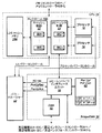
図1を参照すると、システム5の一実施例のブロック図が示されている。図1の実施例において、システム5は外部メモリ12A−12Bに接合された集積回路(IC)10を含む。例示の実施例の場合、集積回路10は中央処理装置(CPU)ブロック14を含み、CPUブロック14は1以上のプロセッサ16とレベル2(L2)キャッシュ18を含む。別の実施例はL2キャッシュ18を含まないか、付加的なレベルのキャッシュを含むの少なくとも何れかである。さらに、2以上のプロセッサ16を含む実施例、及び1つだけのプロセッサ16を含む実施例が検討される。集積回路10は更に1以上の非リアルタイム(NRT)周辺機器20のセットと、1以上のリアルタイム(RT)周辺機器22のセットを含む。例示の実施例の場合、CPUブロック14は、ブリッジ/ダイレクトメモリアクセス(DMA)コントローラ30に結合され、ブリッジ/ダイレクトメモリアクセス(DMA)コントローラ30は1以上の周辺デバイス32A−32C及び/又は1以上の周辺インタフェースコントローラ34に結合する。様々な実施例において、周辺デバイス32及び周辺インタフェースコントローラ34の数は、0から任意の所望の数まで変化する。図1に示したシステム5はG0 38A及びG1 38Bなどの1以上のグラフィックコントローラを含むグラフィックユニットを更に含む。グラフィックユニット当りのグラフィックコントローラの数、及びグラフィックユニットの数は、他の実施例では変わることがある。図1に示すように、システム5は1以上のメモリ物理インタフェース回路(PHY)42A−42Bに結合するメモリコントローラ40を含む。メモリ物理インタフェース回路(PHY)42A−42Bは、メモリ12A−12Bと集積回路10のピン上で通信するよう構成されている。また、メモリコントローラ40は、一組のポート44A−44Eを含む。ポート44A−44Bのそれぞれは、グラフィックコントローラ38A−38Bのそれぞれと結合する。CPUブロック14はポート44Cと結合する。NRT(非リアルタイム)周辺機器20及びRT(リアルタイム)周辺機器22は、ポート44D−44Eとそれぞれ結合する。メモリコントローラ40に含まれるポート数は、メモリコントローラの数であるので、他の実施例において変化し得る。つまり、図1に示すポートよりも多かったり少なかったりするポートがあり得る。メモリPHY42A−42Bの数及び対応するメモリ12A−12Bは、他の実施例においては1又は2以上である。
Referring to
一般的に、ポートは、1以上のソースと通信するメモリコントローラ40上の通信ポイントである。或るケースにおいては、ポートはソース専用となる(例えば、ポート44A−44Bは、グラフィックコントローラ38A−38Bそれぞれに専用となる。)他のケースでは、多数のソース間でポートが共有される(例えば、プロセッサ16はCPUポート44Cを共有し、NRT周辺機器20はNRTポート44Dを共有し、ディスプレイパイプ26及びイメージプロセッサ24などのRT周辺機器はRTポート44Eを共有する。)各ポート44A−44Eは、その各エージェントと通信するインタフェースに結合する。インタフェースは任意のタイプの通信媒体(例えば、バス、ポイントツー・ポイント相互接続など)であり、任意のプロトコルを実装する。メモリコントローラとソース間の相互接続もまた、メッシュ、チップファブリックのネットワーク、共有バス、ポイントツー・ポイント相互接続などの他の任意の所望の相互接続を含む。
In general, a port is a communication point on the memory controller 40 that communicates with one or more sources. In some cases, the ports are dedicated to the source (eg,
プロセッサ16は、どんな命令セットアーキテクチャもインプリメントし、その命令セットアーキテクチャに定義されている命令を実行(演算)する。プロセッサ16はスケーラー、スーパー・スケーラ−、パイプライン、スーパー・パイプライン、順序外、順序どおり、推論、非推論等又はそれらの組み合わせを含む任意のマイクロ・アーキテクチャを用いる。プロセッサ16は、回路を含み、そしてマイクロコーディング テクニックを選択的にインプリメントする。プロセッサ16は1以上のレベル1 キャッシュを含み、そしてその結果、キャッシュ18はL2キャッシュである。他の実施例では、プロセッサ16内のマルチキャッシュレベルを含む。キャッシュ18は階層的に次のレベルに下降する。キャッシュ18は任意のサイズ及びコンフィグレーション(セット関連、ダイレクトマッピングなど)を適用する。
The
グラフィックコントローラ38A−38Bは、グラフィック処理回路である。一般的に、グラフィックコントローラ38A−38Bはフレームバッファに表示されるようオブジェクトをレンダーする。グラフィックコントローラ38A−38Bは、一部又は全てのグラフィックオペレーションを実行するグラフィックソフトウェア、又は或るグラフィックオペレーションのハードウェア加速の少なくともいずれかを演算するグラフィックプロセッサを含む。ハードウェア加速の量及びソフトウェアインプリメンテーションは、各実施例で変化する。
The
NRT周辺機器20は、非リアルタイム周辺機器を含み、そのパフォーマンス及び/又はバンド幅の理由から、メモリ12A−12Bへの独立したアクセスを提供する。つまり、NRT周辺機器20によるアクセスは、CPUブロック14とは独立し、CPUブロックメモリオペレーションとは並行して進む。周辺機器34などの他の周辺機器及び/又は周辺インタフェースコントロール34によって制御された周辺インタフェースと接合する周辺機器も非リアルタイム周辺機器であるが、独立したメモリアクセスを要求していない。NRT周辺機器20の様々な実施例は、ビデオエンコーダ及びデコーダ、スケーラー(scaler)/ローテイター(rotator)回路、画像の圧縮/復元回路などを含む。
NRT peripheral 20 includes non-real-time peripherals and provides independent access to memories 12A-12B for performance and / or bandwidth reasons. That is, the access by the NRT
RT周辺機器22はメモリ待ち時間を要求するリアルタイムをもつ任意の周辺機器を含む。例えば、RT周辺機器はイメージプロセッサ及び1以上のディスプレイパイプを含む。ディスプレイパイプは1以上のフレームをフェッチし、フレームをブレンドし、ディスプレイイメージを形成する回路を含む。ディスプレイパイプは1以上のビデオパイプラインを更に含む。ディスプレイパイプの結果は、ディスプレイスクリーン上のディスプレイスクリーンに表示されるべきピクセルストリームである。ディスプレイスクリーン上のディスプレイに関するディスプレイコントローラにピクセル値を送信する。イメージプロセッサはカメラデータを受信し、メモリに記憶されるイメージにデータを処理する。 The RT peripheral 22 includes any peripheral with real time that requires memory latency. For example, an RT peripheral device includes an image processor and one or more display pipes. The display pipe includes circuitry that fetches one or more frames, blends the frames, and forms a display image. The display pipe further includes one or more video pipelines. The result of the display pipe is a pixel stream to be displayed on the display screen on the display screen. Send the pixel value to the display controller for the display on the display screen. An image processor receives camera data and processes the data into an image stored in memory.
ブリッジ/DMAコントローラ30は周辺機器32及びメモリ空間に対する周辺インタフェースコントローラ34にブリッジする回路を含む。例示の実施例の場合、ブリッジ/DMAコントローラ30は、ブロック14を介した、周辺インタフェースコントローラからCPUメモリコントローラ40へのメモリオペレーションをブリッジする。また、CPUブロック14は、ブリッジされたメモリオペレーション群、及びプロセッサ16/L2キャッシュ18からのメモリオペレーション群間のコヒーレンスを保持する。L2キャッシュ18は、CPUインタフェース上で送信されるプロセッサ16からCPUポート44Cまでのメモリオペレーションによりブリッジされたメモリオペレーションを仲介する。また、ブリッジ/DMAコントローラ30は、周辺機器32及び周辺インタフェースコントローラ34のためにDMAオペレーションを提供し、メモリから及びメモリへデータブロックを転送する。詳細にいうと、DMAコントローラは、周辺機器32及び周辺インタフェースコントローラ34のために、メモリコントローラ40を介して、メモリ12A−12Bから及びメモリ12A−12Bへの転送を実行するよう構成されている。DMAコントローラは、プロセッサ16によってプログラム化され、DMAコントローラは、オペレーションを実行する。例えば、DMAコントローラは、記述子を介してプログラム可能である。この記述子はDMA変換子(例えば、送信元アドレス及び宛先アドレス、サイズなど)を記述するメモリ12A−12Bに記憶されたデータ構造である。或いは又、DMAコントローラはDMAコントローラ(不図示)内のレジスタを介してプログラム化が可能である。
The bridge /
周辺機器32A−32Cは、所望の入力/出力デバイス又は集積回路10に含まれる他のハードウェアデバイスを含む。例えば、周辺機器32A−32Cは、イーサネット(登録商標)MAC(メディアアクセスコントローラ)又は無線フィデリティ(WiFi)などの1以上のネットワークMACといったネットワーク周辺機器を含む。様々なオーディオ処理デバイスを含むオーディオユニットが周辺機器32A−32Cに含まれる。1以上のデジタル信号プロセッサが周辺機器32A−32Cに含まれる。周辺機器32A−32Cは、タイマー、onチップ シークレットメモリ、暗号エンジンやこれらの組み合わせなど他の任意の機能を含む。
Peripherals 32A-32C include desired input / output devices or other hardware devices included in
周辺インタフェースコントローラ34は、任意のタイプの周辺インタフェースに関する任意のコントローラを含む。例えば、周辺インタフェースコントローラは、USBコントローラ、周辺コンポーネント相互接続高速(PCIe)コントローラ、フラッシュメモリインタフェース、汎用入出力(I/O)ピンなどの様々なインタフェースコントローラを含む。 Peripheral interface controller 34 includes any controller for any type of peripheral interface. For example, peripheral interface controllers include various interface controllers such as USB controllers, peripheral component interconnect high speed (PCIe) controllers, flash memory interfaces, and general purpose input / output (I / O) pins.
メモリ12A−12Bは、ダイナミック・ランダムアクセスメモリ(DRAM)、同期DRAM(SDRAM)、ダブルデータレート(DDR,FDDR2,DDR3など)、(mDDR3などの携帯バージョンのSDRAM、LPDDR2などの低パワーバージョンのSDRAMの少なくともいずれかを含む)SDRM、RAMBUS DRAM(RDRAM)、スタティックRAM(SRAM)などの任意のタイプのメモリである。1以上のメモリデバイスがメモリモジュールを形成する回路基板上で接合される。ここで、メモリモジュールとは、単一インライン・メモリモジュール(SIMM)、デュアルインライン・メモリモジュール(DIMM)などである。あるいはまた、デバイスはチップonチップ構成、パッケージonパッケージ構成、又はマルチチップモジュール構成の集積回路10によりマウントされる。
The memories 12A-12B are a dynamic random access memory (DRAM), a synchronous DRAM (SDRAM), a double data rate (DDR, FDDR2, DDR3, etc.), a portable version SDRAM such as mDDR3, and a low power version SDRAM such as LPDDR2. Any type of memory such as SDRM, RAMBUS DRAM (RDRAM), static RAM (SRAM). One or more memory devices are bonded on the circuit board forming the memory module. Here, the memory module is a single inline memory module (SIMM), a dual inline memory module (DIMM), or the like. Alternatively, the device is mounted by an
メモリPHY42A−42Bは、メモリ12A−12Bに対して低レベル周辺インタフェースを扱う。例えば、メモリPHY42A−42Bは、同期DRAMメモリなどに正確なクロッキング(clocking)用の信号タイミングに責任を負う。一実施例において、メモリPHY42A−42Bは、集積回路10内に供給されるクロックをロックするよう構成され、そしてメモリ12により用いられるクロックを生成するよう構成される。
他の実施例は、図1で示すコンポーネント及び/又は他のコンポーネントのサブセット又はスーパーセットを含むコンポーネントの組み合わせを含むことに留意されたい。所与のコンポーネントの一実例が図1に示される一方で、他の実施例は所与のコンポーネントの1以上の実例を含む。同様に、発明の詳細な説明の全体を通して、所与のコンポーネントの1以上の実例は、たとえ1つしか示されていないとしても、1つの実例を含む実施例を含み、複数の実例が示される場合にも用いられる。 It should be noted that other embodiments include combinations of components including those shown in FIG. 1 and / or a subset or superset of other components. An example of a given component is shown in FIG. 1, while other embodiments include one or more instances of a given component. Similarly, throughout the detailed description of the invention, more than one instance of a given component may be illustrated, including an embodiment including one instance, even if only one is shown. Also used in cases.
L2キャッシュのパワーアップ/パワーダウン
図2を参照すると、集積回路10の一部の実施例のブロック図が詳細に示されている。特に、CPUブロック14及びブリッジ/DMAコントローラ30がパワーマネージャー50と共に示されている。CPUブロック14はプロセッサ16及びL2キャッシュ18を含む。図2の実施例の場合、L2キャッシュ18はL2キャッシュコントロール18A及びL2キャッシュメモリ18Bとして示されている。L2キャッシュコントロール18Aは、キャッシュ制御回路52及びコヒーレンス制御回路54を含む。キャッシュ制御回路52及びコヒーレンス制御回路54のそれぞれは、コンフィグレーションレジスタ56A−56Dなどのコンフィグレーションレジスタを含む。プロセッサ16は、L2キャッシュコントロール18A、特にコヒーレンス制御回路54と結合される。コヒーレンス制御回路54はキャッシュ制御回路52と結合される。L2キャッシュコントロール18A及び特にキャッシュ制御回路52は、L2キャッシュメモリ18Bと結合される。L2キャッシュコントロール18Aは更にメモリコントローラ40(例えば、図1のCPUポート44C)と結合する。パワーマネージャー50は、L2キャッシュコントロール18A(例えば、図2のL2パワー制御信号)及びプロセッサ16(例えば、図2のプロセッサパワー制御信号)と結合する。
L2 Cache Power Up / Power Down Referring to FIG. 2, a block diagram of some embodiments of
ブリッジ/DMAコントローラ30は、コヒーレントI/Oインタフェースユニット(CIF)58、パワーアップ/パワーダウンメモリ60、DMAコントローラ62を含む。CIF58は、ワーアップ/パワーダウンメモリ60と、DMAコントローラ62と、L2キャッシュコントロール18Aと(特に、コヒーレンス制御回路54)、パワーマネージャー50と(例えば、図2のI/Oアイドル、PWrUpReq、PWrUpAck信号を介して)、周辺回路32A−32Cと、周辺インタフェースコントローラ34との少なくとも何れか一つと結合される。DMAコントローラ62は更に、周辺回路32A−32Cと、周辺インタフェースコントローラ34と結合する。一実施例において、DMAコントローラ62及びCIF58は、周辺回路32A−32C及び/又は周辺インタフェースコントローラ34の各サブセットと結合する。サブセットはオーバーラップし得る(例えば、ある周辺機器/周辺インタフェースコントローラは、DMAを介して及びCIF58との直接通信を介しての両方によりメモリと通信するよう構成されている)。他の周辺機器/周辺インタフェースコントローラは、DMAを介してのみ又はCIF58に直接送信されたオペレーションを介してのみメモリと通信する。
The bridge /
コンフィグレーションレジスタ56A−56Dはソフトウェアによってプログラム化され、キャッシュ制御回路52及びコヒーレンス制御回路54のオペレーションの様々な面を制御する。一般的に、回路ブロックは、様々なプログラム可能なコンフィグレーションの間でソフトウェアを選択できるようにするコンフィグレーションレジスタを実装する。例えば、L2キャッシュ18のサイズ及びコンフィグレーションは、或る所定の最大数の範囲内で選択可能であう。キャッシュの書込みスルー/書込みバックオペレーションが構成される。コヒーレントモードはコンフィグレーションレジスタ56A−56Dを通じて有効化されコントロールされる。或る実施例において、キャッシュ制御回路52だけがキャッシュコンフィグレーションレジスタ56A−56Dを含むか、若しくは、コヒーレンス制御回路54だけがキャッシュコンフィグレーションレジスタを56A−56Dを含む。
Configuration registers 56A-56D are programmed by software to control various aspects of the operation of
L2キャッシュ18がパワーダウンされる場合、コンフィグレーションレジスタ56A−56Dの少なくとも幾つかに記憶されたコンフィグレーションデータが失われる。L2キャッシュ18がパワーダウンされ、その後にパワーアップされた後にコンフィグレーションを復活させるため、コンフィグレーションデータをパワーアップ/パワーダウンメモリ60に記憶する。例えば、ソフトウェアがコンフィグレーションレジスタ56A−56Dをパワーアップで復活されるはずの値でプログラムされるとき、ソフトウェアはパワーアップ/パワーダウンメモリ60に値を書込む。同様に、パワーダウンの前に実行される、コンフィグレーションレジスタ書込み又は他のレジスタ書込みがある。例えば、パワーダウンの前に、(任意の未処理メモリオペレーション若しくは他の通信が完了することを保証しながら)レジスタがL2キャッシュ18を同期させる同期コマンドで書込まれる。
When the
パワーアップ/パワーダウンイベントの間中、CIF58はパワーアップ/パワーダウンメモリ60からオペレーションを読出すように構成される。パワーマネージャー50はCIF58に対してパワーアップ又はパワーダウンイベントを信号送信するよう構成され、そしてCIF58はメモリ60を読出して対応のイベントをL2キャッシュ18に送信するよう構成される。オペレーションが終了すると、CIF58はパワーマネージャー50に対して終了報告を通信するよう構成される。これに応答して、パワーマネージャー50はパワーアップ/パワーダウンイベントを完了させる。
During a power up / power down event,
パワーマネージャー50及びCIF58の間で任意の通信が実行される。例示した実施例においては、パワーマネージャー50はPwrUpReq信号を用いながらパワーアップ若しくはパワーダウンイベントを信号送信する。詳しく言うと、パワーマネージャー50は、L2キャッシュ18がパワーアップされることを示すためにPwrUpReq信号をアクティブな状態にし、L2キャッシュ18がパワーダウンされることを示すためにPwrUpReq信号をアクティブでない状態に構成される。PwrUpReq信号のアクティブ状態にあわせて、CIF58の間58は、パワーアップオペレーションとして示されるパワーアップ/パワーダウンメモリ60内の任意のオペレーションを読出して、このオペレーションをL2キャッシュ18に通信するよう構成されている。CIF58は、オペレーションが完了したことを決定し(例えば、各レジスタ書込みオペレーションに対応する書込み完了を受信すること)、そしてパワーアップイベントを肯定応答するためにCIF58はPwrUpAck信号をアクティブ状態にする。パワーマネージャー50は、PwrUpAck信号のアクティブ状態に反応してL2キャッシュ18への通信を再びイネーブルする。
Arbitrary communication is executed between the
L2キャッシュ18をパワーダウンすることはキャッシュ制御回路52を少なくともパワーダウンすることを含む。ある実施例においては、コヒーレンス制御回路54もまたパワーダウンされる。L2キャッシュ18Bは幾つかの実施例においては、キャッシュ内のキャッシュ状態(例えば、メモリからの様々なキャッシュブロック、タグ・有効性・コヒーレンス状態などのキャッシュブロック)を保持しながらパワーオンされたままである。或いはまた、L2キャッシュ18Bは、L2キャッシュ18をパワーダウンする一部としてパワーダウンされている。パワーダウンされた回路/メモリは、パワーアップイベントに応答して再びパワーアップされ得る。
Powering down the
パワーアップ/パワーダウンメモリ60は任意の半導体ストレージから形成される。例えば、ソフトウェアによって読出され/書込まれるマルチレジスタが提供される。他の実施例は、他の形式のストレージ(例えば、スタティックRAMなどのランダムアクセスメモリ(RAM))を用いる。
The power-up / power-
パワーアップ/パワーダウンメモリ60は一般的にマルチエントリを含む。図2のメモリ60に典型的な2つのエントリを示す。例示の実施例の場合、パワーアップ/パワーダウンメモリ60内の各エントリは、図2のエントリにおいて、フィールドとデータフィールドとして示したように、アドレスとデータの組を含む。アドレスは書込まれるコンフィグレーションレジスタを識別し、データはそのコンフィグレーションレジスタに書込まれる値である。アドレスは相対的なものであり(例えば、アドレスはL2キャッシュコントロール18Aに対応するベースアドレスからのオフセットであったり、又は、コヒーレンス制御回路54及び/又はキャッシュ制御回路52のためのベースアドレスである)。或いはまた、このアドレスは、対応のレジスタ56A−56Dに対する書込みオペレーションにある、プロセッサが送信したであろう完全アドレスである。また、各エントリは、エントリが有効情報を記憶しているか否かを示す有効ビット(V)を含む。さらに、この実施例の場合、各エントリは、パワーダウン中又はパワーアップ中にコンフィグレーションレジスタ書込みが実行されるかどうかを示すパワーダウン(D)フィールドを含む。Dフィールド内のDビットはパワーダウンレジスタ書込みを示すためにセットされ、パワーアップレジスタ書込みを示すことが明らかである。他の実施例は、パワーダウン及びパワーアップに関して異なるメモリを使用したり、又は既知の形式でメモリを分割したりし、そしてDフィールドは各エントリに含まれていないかもしれない。
The power-up / power-
一実施例において、ソフトウェアは、パワーアップ/パワーダウンメモリ60の初期エントリにパワーダウンアドレス/データの組を書込み、そしてその後のエントリにパワーアップアドレス/データの組を書込むことが見込まれている。このような実施例の場合、パワーダウンイベントに応答して、Dビットをクリアさせるエントリに遭遇するまで、CIF58は初期エントリをもつオペレーション始めを読出す。CIF58はポインタをエントリに残し、パワーアップイベントに応答して示されたエントリからパワーアップオペレーションを読出すことを始める(その後で、そのポインタは初期エントリに対するポイントに再びリセットされる)。
In one embodiment, the software is expected to write the power-down address / data pair to the initial entry of power-up / power-
パワーアップ/パワーダウンメモリ60がコンフィグレーションレジスタ書込みを記憶する一方で、他の実施例は実行されるべき任意のタイプのオペレーション(例えば、レジスタ書込み、レジスタ読出し、コマンドなど)を記憶する。したがって、L2キャッシュ18をパワーアップし及びパワーダウンするためのフレキシブルなメカニズムがサポートされる。このメカニズムはL2キャッシュ18をパワーアップし又はパワーダウンすることをサポートしながら、プロセッサ16を(プロセッサ16を起動することなく)パワーダウンする。くわえて、オペレーションがメモリ60内でプログラム可能であることから、実行されるはずのオペレーションは変更され、そしてオペレーションの順序が変更される。したがって、メカニズム自体がハードウェアで動作かするとしても、そのメカニズムはソフトウェア変更を介して(オペレーティングにエラーがあれば)訂正される。
While the power-up / power-
一般的に、キャッシュ制御回路52はL2キャッシュ18Bにアクセスすることを管理するよう構成される。このキャッシュ制御回路52は、キャッシュアクセスに関するヒット/ミスを検出し、ミスのためのキャッシュ充填を開始し、L2キャッシュ18内の置き換えポリシーを管理したりする。コヒーレンス制御回路54は、プロセッサ16のメモリオペレーションのために、そしてCIF58からのメモリオペレーションのために(例えば、DMAコントローラ62からのDMAオペレーション及び/又は周辺機器32A−32Cから直接受信した他のメモリオペレーション及び/又は周辺インタフェースコントローラ34)、CPUブロック14におけるキャッシュコヒーレントをコントロールする。コヒーレンス制御回路54は、プロセッサ16内のキャッシュに関するスヌープ(詮索)タグを保持し、そしてキャッシュコヒーレンス目的のためにL2キャッシュメモリ18Bを詮索するため、キャッシュコントロールプロセッサ16に対するキャッシュアクセスを生成するよう構成される。
In general, the
パワーマネージャー50は、プロセッサ16及びL2キャッシュ18、さらには集積回路10における他の様々なアクティビティ(不図示)をモニタリングするよう構成される。パワーマネージャー50は、プロセッサ16のパワーアップ又はダウンを含むパワー状態を、プロセッサパワー制御信号を介してコントロールする。プロセッサ16は様々な実施例において独立して又は同期してパワーアップ又はパワーダウンされる。
The
パワーマネージャー50は、L2キャッシュ18がアイドル(遊休)状態である場合、L2キャッシュ18をパワーダウンする。パワーマネージャー50は、L2キャッシュ18が様々な態様でアイドル(遊休)状態であることを検出する。例えば、プロセッサ16がパワーダウンされ、その結果、どのメモリオペレーションもプロセッサ16から見込まれていないことにパワーマネージャー50は気づく。さらに、パワーマネージャー50は、ブリッジ/DMAコントローラが少なくともメモリオペレーションに関してアイドル状態であることを検出する。例示の実施例の場合、CIF58はI/Oアイドル信号を生成する。CIF58は、周辺機器32A−32C及び/又は周辺インタフェースコントローラ34からのメモリオペレーションがないということを示すI/Oアイドル信号(DMAコントローラ62からの何のメモリオペレーションもないことを含む)をアサートする。一実施例において、CIF58は、パワーマネージャー50へI/Oアイドル信号をアサートする前に、プログラム可能な連続クロックサイクル数に関するメモリオペレーションがないことを検出する。一実施例において、CIF58はI/Oアイドル信号をアサートしないよう構成される。しかしながら、CIF58は、パワーマネージャー50から、メモリオペレーションが送信され得る知らせを待つ。その知らせは、パワーマネージャー50がメモリオペレーションを受信する前にパワーダウンイベントを開始したという競争状態を避け、その結果、パワーダウンイベントの一環として失われることとなるL2キャッシュ18へのメモリオペレーション送信を避ける。一実施例において、準備完了信号(不図示)がパワーマネージャー50によって提供され、I/Oアイドル信号のアサーション(及びアサーション停止)の後に、L2キャッシュ18がメモリオペレーションにとって準備完了であることを示す。
The
次に、図3〜6を参照すると、パワーマネージャー50及びL2キャッシュ18をパワーアップ及びダウンさせるCIF58のオペレーションをあらわすフローチャートが示されている。理解を容易にするために特定の順序でブロックを示しているが、他の順序も用いられる。パワーマネージャー50及び/又はCIF58の組み合わせ論理において並行してブロックが実行される。ブロック、ブロックの組み合わせ、及び/又はフローチャートは、全体として、マルチクロックサイクルでパイプラインされる。メモリコントローラ40は、図19に示すオペレーションを実行するように構成される。パワーマネージャー50及び/又はCIF58はフローチャートに示したオペレーションを実行するよう構成される。詳細には、パワーマネージャー50及び/又はCIF58は、図示したオペレーションを実行するハードウェア回路を含む。
Referring now to FIGS. 3-6, there is shown a flow chart representing the operation of the
図3は、パワーダウンイベントに関するパワーマネージャー50の一実施例におけるオペレーションを示したフローチャートである。パワーマネージャー50は、プロセッサ16がパワーダウンし(判断ブロック70の「Yes」)、かつ、CIF5858が信号送信されたI/Oアイドルをもつ場合(判断ブロック72の「Yes」)、パワーダウンイベントが生じたことを決定する。その場合、パワーマネージャー50は、CIF58にPwrUpReq信号のアサート停止をして(ブロック74)、パワーダウンイベントを開始する。パワーマネージャー50は、CIF58からの肯定応答(Ack)を待ち(判断ブロック76)、そしてPwrUpAckのアサート停止に応答して(判断ブロック76の「Yes」)、パワーマネージャー50はL2キャッシュをパワーダウンさせる(ブロック78)。
FIG. 3 is a flowchart illustrating operations in one embodiment of the
図4は、パワーダウンイベントに関するCIF58の一実施例におけるオペレーションを示したフローチャートである。パワーダウンイベントのCIF58処理は、パワーマネージャー50からのPwrUpReq信号をアサーション停止することに応答して開始する(判断ブロック80の「Yes」)。CIF58は、パワーアップ/パワーダウンメモリ60から初期エンティティを読出し(ブロック82)、そのエンティティが有効であり且つパワーダウンイベントに関するものであるか否かを決定する(V及びDセット、判断ブロック84)。そうである場合(判断ブロック84が「Yes」)、CIF58はアドレス/データの組をL2コントロール18Aに送信して、識別されたコンフィグレーションレジスタ56A−56Dをアップデートする(ブロック86)とともに、次のエントリをメモリ60に読出す(ブロック82)。そうでない場合(判断ブロック84が「No」)、CIF58はすべてのコンフィグレーションレジスタ書込みに対する書込み応答がL2コントロール18Aから受信されたかどうかを決定する(判断ブロック88の「Yes」)。応答が受信されていた場合(判断ブロック80の「Yes」)、L2コントロール18Aはパワーダウンのために準備され、そしてCIF58はパワーダウン要求を肯定応答するためにPwrUpAck信号をアサート停止にする(ブロック90)。
FIG. 4 is a flowchart illustrating operations in one embodiment of
図5は、パワーアップイベントに関するパワーマネージャー50のオペレーションを示したフローチャートである。パワーマネージャー50は、プロセッサ16がパワーアップされる場合若しくはメモリオペレーションがCIF58に受信される場合に(I/Oアイドルのアサート停止を生じさせることになる)、パワーアップイベントが生じることを決定する。パワーマネージャー50は、L2キャッシュコントロールをパワーアップし(ブロック100)、そしてパワーが安定するまで待つ。パワーマネージャー50はPwrUpReq信号をアサートし(ブロック102)、L2キャッシュ18が初期化されて再び通信の準備完了であることを決定するために、アサートされるはずのPwrUpAck信号を待つ(ブロック104)。
FIG. 5 is a flowchart showing the operation of the
図6は、パワーアップイベントに関するCIF58のオペレーションを示したフローチャートである。CIF58は、PwrUpReq信号のアサーションに応答して開始する(判断ブロック110の「Yes」)。CIF58は、パワーアップ/パワーダウンメモリ60内の次のエンティティを読出す(ブロック112)。そのエンティティが有効であり且つパワーアップオペレーションであるならば(Vセット及びDクリア、判断ブロック114の「Yes」)、CIF58はコンフィグレーションレジスタ書込みをL2キャッシュコントロール18Aに送信し(ブロック116)、そしてメモリ60内の次のエンティティを読出す(ブロック112)。エンティティが有効ではないか又はパワーダウンオペレーションであるならば(判断ブロック114の「No」)、CIF58はレジスタ書込みに対する応答が受信されたかどうかを決定する(判断ブロック118)。応答が受信されていた場合(判断ブロック118の「Yes」)、CIF58はPwrUpAck信号をアサートする(ブロック120)。
FIG. 6 is a flowchart showing the operation of the
或る実施例において、パワーマネージャー50は、パワーアップイベントの処理の間中、L2キャッシュ18がパワーダウンされているかを決定したり、又はパワーダウンイベントの処理の間中、L2キャッシュ18がパワーアップされているかを決定する。幾つかのインプレメンテ−ション(実装例)において、パワーマネージャー50は、新たな遷移を開始する前に、進行中の遷移を完了できるようにする。別のインプレメンテ−ションにおいては、パワーマネージャー50は、(例えば、PwrUpReq信号の状態を変化させることによって)決定がなされると新たな遷移を信号送信するよう構成される。CIF58は、状態変化を検出するためのPwrUpReq信号をモニタリングし、進行中のイベントを処理することを終わらせる。CIF58は、更なる処理をすることなく変化した状態を肯定応答したり、或いは新たなイベントを処理(新たなイベントに関するレジスタ書込みを実行すること)したりのいずれかを行なう。
In some embodiments, the
図7は、一実施例に関するL2キャッシュ18のパワーダウン及びパワーアップシーケンスを示すタイミング図である。時間(タイム)は、図7の左から右に任意の単位で増加する。このL2キャッシュ18はタイミング図の開始でパワーアップしオペレーティングされ(ブロック130)、そしてPwrUpReq及びPwrUpAck信号の両方ともがアサートされる。パワーマネージャー50は、L2キャッシュがパワーダウンされているかを決定し、PwrUpReq信号をアサート停止にする(点線132)。CIF58は、レジスタ書込みを送信し応答を収集することを開始する。(ブロック134)。ひとたび書込みが完了して応答が受信されると、CIF58はPwrUpAck信号をアサート停止にし(点線136)、そしてL2キャッシュ18はパワーダウンされる(ブロック138)。後のポイントで、パワーマネージャー50は、L2キャッシュがパワーアップされているかを決定し、L2キャッシュ18にパワーを確立したあとでPwrUpReq信号をアサートする(点線140)。CIF58はコンフィグレーションレジスタを初期化するためにレジスタ書込みを送信し(ブロック142)、書込みを完了すること及び応答を受信することに反応してPwrUpAck信号をアサートする(点線144)。L2キャッシュ18はパワーアップされ、そしてこのポイントで再びオペレートする(ブロック146)。
FIG. 7 is a timing diagram illustrating a power down and power up sequence of the
図8を参照すると、L2キャッシュコンフィグレーションをアップデートするソフトウェアの一実施例を示すフローチャートが記載されている。例えば、ソフトウェアは、システム5のブート中及び/又はL2キャッシュコンフィグレーションを変更するシステムオペレーション間の他の時点で演算されるコンフィグレーションコードを含む。L2コンフィグレーションコードは図8に示すオペレーションをインプリメントするプロセッサ16の一つで演算される。つまり、L2コンフィグレーションコードは命令を含み、それはプロセッサ16の一つによって演算されるときに図8に示すオペレーションを実行(インプレメント)する。理解を容易にするために特定の順序でブロックを示しているが、他の順序も用いられる。
Referring to FIG. 8, a flowchart illustrating one embodiment of software for updating the L2 cache configuration is described. For example, the software includes configuration code that is computed during
L2キャッシュコンフィグレーションコードはL2キャッシュ18内に1以上のコンフィグレーションレジスタを書込む(ブロック150)。1以上のコンフィグレーションレジスタがL2キャッシュ18中に書込まれることを必要とされるならば(判断ブロック152の「Yes」)、このコードはパワーアップ/パワーダウンメモリ60に対するコンフィグレーションレジスタのアドレス及び対応データを書込む(ブロック154)。例えば、L2キャッシュ18の同期を生じさせるレジスタ書込みを含む。コードは、パワーダウン書込みにより各エントリ書込みにV及びDビットをセットする。1以上のコンフィグレーションレジスタがL2キャッシュ18のパワーアップ中に回復される場合(判断ブロック156の「Yes」)、このコードはパワーアップ/パワーダウンメモリ60に対するコンフィグレーションレジスタのアドレス及び対応データを書込み、そして各エントリにVビットをセットしてDビットをクリアする(ブロック158)。幾つかの実施例において、パワーダウン書込み及びパワーアップ書込みの両方に、同じコンフィグレーションレジスタを含むことに留意されたい。
The L2 cache configuration code writes one or more configuration registers in the L2 cache 18 (block 150). If more than one configuration register is required to be written into the L2 cache 18 (
別の実施例において、CIF58は、コンフィグレーションレジスタ56A−56Dに対する書込み(又はパワーアップイベントに再び記憶され及び/又はパワーダウンイベントに書込まれるはずのコンフィグレーションレジスタのサブセット)を検出するよう構成される。CIF58は、レジスタに書かれた値をパワーアップ/パワーダウンメモリ60において自動的にキャプチャーする。その結果、L2コンフィグレーションコードはメモリ60への書込みを明示的に実行する必要はない。このような実施例の場合、L2コンフィグレーションコードは、上述した自動的なキャプチャーに加えて、メモリ60をアップデートこともできる。L2コンフィグレーションコードは、例えば、パワーダウンイベントのための同期コマンドを挿入する。
In another embodiment,
図9を参照すると、コンピュータアクセス可能な記憶媒体200のブロック図が示されている。一般的に言って、コンピュータアクセス可能な記憶媒体は、コンピュータに命令及び/又はデータを提供するために使用する間にコンピュータがアクセスする任意の記憶媒体を含む。例えば、コンピュータアクセス可能な記憶媒体は、例えばディスク(固定若しくはリムーバブル)、テープ、CD−ROMやDVD−ROM、CR−R、CD−RW、DVD−R、DVD−RW、又はブルーレイといった磁気や光メディアの記憶媒体を含む。記憶媒体は、RAN(例えば、同期ダイナミックRAM(SDRAM)、ダブルデータレート(DDR,FDDR2,DDR3など)、SDRAM、低パワーDDR(LPDDR2など)、SDRAM、RambusDRAM(RDRAM)、スタティックRAM(SRAM)など)、ROM、フラッシュメモリ、ユニバーサルバス(USB)インタフェースなどの周辺インタフェースを介してアクセス可能な不揮発性メモリ(例えば、フラッシュメモリ)。記憶媒体は、マイクロマシン技術(MEMES)の他に、ネットワーク及び/又は無線リンクなどの通信媒体を介してアクセス可能な記憶媒体を含む。図9のコンピュータアクセス可能な記憶媒体200は、L2コンフィグレーションコードを記憶し、それは図8のフローチャートを実行する。一般的に、コンピュータアクセス可能な記憶媒体200は命令のセットを記憶し、それは実行時において、図8のフローチャートの一部又は全部を実行する。キャリア媒体は、コンピュータアクセス可能な記憶媒体と、優先若しくは無線伝送の伝送媒体とを含む。 Referring to FIG. 9, a block diagram of a computer accessible storage medium 200 is shown. Generally speaking, computer-accessible storage media includes any storage media that the computer accesses while in use to provide instructions and / or data to the computer. For example, a computer-accessible storage medium is, for example, a disk (fixed or removable), a tape, a CD-ROM, a DVD-ROM, a CR-R, a CD-RW, a DVD-R, a DVD-RW, or a Blu-ray, such as magnetic or optical. Includes media storage media. Storage media include RAN (eg, synchronous dynamic RAM (SDRAM), double data rate (DDR, FDDR2, DDR3, etc.), SDRAM, low power DDR (LPDDR2, etc.), SDRAM, Rambus DRAM (RDRAM), static RAM (SRAM), etc. ), Non-volatile memory (e.g. flash memory) accessible via peripheral interfaces such as ROM, flash memory, universal bus (USB) interface. Storage media include storage media accessible via communication media such as networks and / or wireless links in addition to micromachine technology (MEMES). The computer-accessible storage medium 200 of FIG. 9 stores the L2 configuration code, which executes the flowchart of FIG. In general, computer-accessible storage medium 200 stores a set of instructions that, when executed, execute some or all of the flowchart of FIG. Carrier media include computer-accessible storage media and priority or wireless transmission media.
図10を参照すると、システム350の一実施例のブロック図が示されている。例示の実施例において、システム350は、外部メモリ12に結合された集積回路10の少なくとも1つのインスタンスを含む。外部メモリ352は図1に関して上述した主メモリサブシステムを形成する(例えば、外部メモリ352はメモリ12A−12Bを含む)。集積回路10は1以上の周辺機器354及び外部メモリ12に結合する。電源供給356が提供され、集積回路358に電圧を供給するとともに、メモリ352及び/又は周辺機器354に電圧を供給する。幾つかの実施例において、1より多い集積回路10のインスタンスが含まれる(そして同様に、1より多い外部メモリ352が含まれる)。
Referring to FIG. 10, a block diagram of one embodiment of
メモリ352は任意のタイプのメモリである。例えば、ダイナミックランダムアクセスメモリ(DRAM)、同期ダイナミックRAM(SDRAM)、ダブルデータレート(DDR,FDDR2,DDR3など)、SDRAM(mDDR3などのSDRAMのモバイルバージョン、及び/又はLPDDR2などのSDRAMの低パワーバージョンを含む)、RAMBUS DRAM(RDRAM)、スタティックRAM(SRAM)などである。1以上のメモリデバイスは、単一インラインメモリモジュール(SIMM)、デュアルインラインメモリモジュール(DIMM)などのメモリモジュールを形成する回路基板上に接合される。或いはまた、デバイスはチップオンチップコンフィグレーション、パッケージオンパッケージコンフィグレーション、マルチチップモジュールコンフィグレーションの集積回路10によりマウントされる。
Memory 352 is any type of memory. For example, dynamic random access memory (DRAM), synchronous dynamic RAM (SDRAM), double data rate (DDR, FDDR2, DDR3, etc.), SDRAM (SDRAM mobile version such as mDDR3, and / or low power version of SDRAM such as LPDDR2) RAMBUS DRAM (RDRAM), static RAM (SRAM), and the like. One or more memory devices are bonded onto a circuit board that forms a memory module, such as a single inline memory module (SIMM), a dual inline memory module (DIMM), or the like. Alternatively, the device is mounted by an
周辺機器354はシステム350のタイプによって望しい回路を含む。例えば、一実施例において、システム350はモバイル機器(例えば、携帯情報端末(PDA)、スマートフォンなど)であり、そして周辺機器354は様々なタイプの無線通信(例えば、wifi、bluetooth、セルラー、GPSなど)を含む。また、周辺機器354はRAM記憶媒体、固体記憶媒体、ディスク記憶媒体を含む追加的ストレージを含む。周辺機器354はディスプレイスクリーンなど(例えば、タッチディスプレイスクリーン又はマルチタッチディスプレイスクリーン、キーボード若しくは他の入力デバイス、マイクロフォン、スピーカー)のユーザインタフェース機器を含む。他の実施例では、システム350は任意のタイプのコンピュータシステム(例えば、デスクトップPC、ラップトップ、ワークステーション、ネットトップなど)である。
上述したように開示が理解される場合、様々なバリエーション及び修正が当業者にとって明らかとなる。添付の特許請求の範囲はこのようなバリエーション及び修正をとらえるために解釈されることを意図している。 Various variations and modifications will become apparent to those skilled in the art once the disclosure is understood as described above. It is intended that the appended claims be construed to capture such variations and modifications.
Claims (17)
前記メモリ及び制御回路を含むシステム内のプロセッサがパワーダウンされるときの間に、前記回路ブロックをパワーダウンさせる要求を受信するために接合された制御回路であって、前記要求に応答して前記第1の組のオペレーションに対応する前記メモリ内で識別され且つ前記少なくとも1つのレジスタ書込みオペレーションを含むオペレーションを実行する前記制御回路と、
を含む装置。 A memory for storing a first set of operations to be performed before, data identifying a second set of operations to be subsequently performed to said circuit block is powered up to power down the circuit block The first set of operations performed before powering down the circuit block includes the memory including at least one register write operation on a register in the circuit block;
A control circuit joined to receive a request to power down the circuit block while a processor in the system including the memory and control circuit is powered down, responsive to the request; The control circuit performing an operation identified in the memory corresponding to a first set of operations and including the at least one register write operation ;
Including the device.
前記第2の組のオペレーションは、前記回路ブロックにおける複数の第2レジスタに関する複数の第2のレジスタ書込みオペレーションを含み、前記メモリ内のデータは、前記複数の第2レジスタを識別する複数の第2アドレスと、前記複数の第2アドレスに書込まれる複数の第2データ値とを含む、
ことを特徴とする請求項1に記載の装置。 The first set of operations includes a plurality of first register write operations for a plurality of first registers in the circuit block, the plurality of first register write operations including the at least one register write operation; The data in the memory includes a plurality of first addresses identifying the plurality of first registers, and a plurality of first data values written to the plurality of first addresses,
The second set of operations includes a plurality of second register write operations for a plurality of second registers in the circuit block, and the data in the memory includes a plurality of second registers identifying the plurality of second registers. An address and a plurality of second data values written to the plurality of second addresses;
The apparatus according to claim 1.
前記制御回路と前記メモリは前記キャッシュに結合されたブリッジ内に含まれ、前記メモリは、前記第1の組のオペレーション及び前記第2の組のオペレーションをあらわすデータによりプログラム可能である複数のレジスタを含み、前記ブリッジは、前記キャッシュに関するパワーダウンイベントに応答して前記第1の組のオペレーションを実行し、そして前記キャッシュに関するパワーアップイベントに応答して前記第2の組のオペレーションを実行する、前記システム。 A system comprising one or more processors and the apparatus of claim 1 wherein the circuit block is a cache coupled to the one or more processors.
The control circuit and the memory are included in a bridge coupled to the cache, and the memory includes a plurality of registers programmable with data representing the first set of operations and the second set of operations. The bridge performs the first set of operations in response to a power down event for the cache and performs the second set of operations in response to a power up event for the cache; system.
前記キャッシュの1以上のコンフィグレーションレジスタを初期化し、
パワーダウンイベント及びその後のパワーアップイベントに引き続いて前記コンフィグレーションレジスタを自動的に元の状態に戻すために、前記ブリッジ内のメモリに前記コンフィグレーションレジスタに関する対応データを書込む、
処理を行なう請求項6に記載のシステム。 In response to executing the plurality of instructions, a first processor of the one or more processors is
Initialize one or more configuration registers of the cache;
In order to automatically restore the configuration register to its original state following a power-down event and a subsequent power-up event, the corresponding data related to the configuration register is written to the memory in the bridge.
The system according to claim 6, wherein the processing is performed.
各コンフィグレーションレジスタに関する各対応データに対して、前記対応データがパワーアップイベント中に書込まれることを示すフラグを書込むよう更に構成される、請求項10に記載のシステム。 In response to executing the plurality of instructions, the first processor includes:
The system of claim 10, further configured to write a flag indicating that the corresponding data is written during a power-up event for each corresponding data for each configuration register.
パワーダウンイベント中に実行される1以上の追加的レジスタ書込みオペレーションに対応する前記ブリッジ内のメモリにデータを書込み、
前記1以上の追加的レジスタ書込みオペレーションがパワーダウンイベント中に実行されることを示す、前記追加的レジスタ書込みオペレーション対応フラグを書込むよう更に構成される、請求項10に記載のシステム。 In response to executing the plurality of instructions, the first processor includes:
Write data to memory in the bridge corresponding to one or more additional register write operations performed during a power down event;
The system of claim 10, further configured to write the additional register write operation support flag indicating that the one or more additional register write operations are performed during a power down event.
前記回路ブロック及び1以上の周辺機器に結合される制御回路に要求を発行する処理と、
前記回路ブロック内の1以上のコンフィグレーションレジスタを初期化するために、前記制御回路が、前記制御回路に記憶された複数のオペレーションを実行することによって前記要求に応答する処理と、
パワーダウンされる前記回路ブロックを検出する処理と、
パワーダウンされる前記回路ブロックを検出することに応答して、前記制御回路へ第2の要求を発行する処理と、
前記制御回路が、前記制御回路に記憶された1以上の第2のオペレーションを実行することによって前記第2の要求に応答する処理であって、前記1以上の第2のオペレーションがキャッシュ内の第1のコンファイルグレーションレジスタに対する第1の書込みオペレーションを含む当該応答する処理と、を含む方法。 Detecting that the circuit block is powered up in a system including one or more processors coupled to the circuit block;
Processing to issue a request to a control circuit coupled to the circuit block and one or more peripheral devices;
A process in which the control circuit responds to the request by performing a plurality of operations stored in the control circuit to initialize one or more configuration registers in the circuit block;
Detecting the circuit block to be powered down;
In response to detecting the circuit block being powered down, issuing a second request to the control circuit;
A process in which the control circuit responds to the second request by executing one or more second operations stored in the control circuit, wherein the one or more second operations are in a cache; And responsive processing including a first write operation to one configuration register .
前記決定に応答して、前記制御回路は前記第2の要求を肯定応答する処理と、
前記ブリッジの肯定応答に応答して前記回路ブロックをパワーダウンさせる処理と、
を更に含む、請求項14に記載の方法。 Processing by which the control circuit determines that the one or more second operations have been completed;
In response to the determination, the control circuit acknowledges the second request;
Processing to power down the circuit block in response to an acknowledgment of the bridge;
15. The method of claim 14 , further comprising:
Applications Claiming Priority (2)
| Application Number | Priority Date | Filing Date | Title |
|---|---|---|---|
| US12/894,516 | 2010-09-30 | ||
| US12/894,516 US8806232B2 (en) | 2010-09-30 | 2010-09-30 | Systems and method for hardware dynamic cache power management via bridge and power manager |
Publications (2)
| Publication Number | Publication Date |
|---|---|
| JP2012079320A JP2012079320A (en) | 2012-04-19 |
| JP5537533B2 true JP5537533B2 (en) | 2014-07-02 |
Family
ID=44785486
Family Applications (1)
| Application Number | Title | Priority Date | Filing Date |
|---|---|---|---|
| JP2011230166A Active JP5537533B2 (en) | 2010-09-30 | 2011-09-30 | Hardware dynamic cache power management |
Country Status (9)
| Country | Link |
|---|---|
| US (1) | US8806232B2 (en) |
| EP (1) | EP2437138A3 (en) |
| JP (1) | JP5537533B2 (en) |
| KR (1) | KR101317526B1 (en) |
| CN (1) | CN102646446B (en) |
| GB (1) | GB2484204B (en) |
| NL (1) | NL2007481C2 (en) |
| TW (1) | TWI483265B (en) |
| WO (1) | WO2012050773A1 (en) |
Families Citing this family (14)
| Publication number | Priority date | Publication date | Assignee | Title |
|---|---|---|---|---|
| US9285856B2 (en) * | 2010-12-21 | 2016-03-15 | Qualcomm Incorporated | Method and system for rapid entry into and for rapid exiting from sleep states for processors of a portable computing device |
| US9104499B2 (en) | 2010-12-21 | 2015-08-11 | Qualcomm Incorporated | System for minimizing resource latency between processor application states in a portable computing device by scheduling resource state set transitions |
| US8954980B2 (en) | 2011-11-11 | 2015-02-10 | Qualcomm Incorporated | Conserving power through work load estimation for a portable computing device using scheduled resource set transitions |
| US9513693B2 (en) | 2014-03-25 | 2016-12-06 | Apple Inc. | L2 cache retention mode |
| BR112017001975B1 (en) * | 2014-07-30 | 2023-02-28 | Movidius Limited | LOW POWER COMPUTATIONAL IMAGING |
| GB2539459A (en) * | 2015-06-16 | 2016-12-21 | Nordic Semiconductor Asa | Waveform generation |
| US10156887B2 (en) * | 2016-09-29 | 2018-12-18 | Qualcomm Incorporated | Cache memory clock generation circuits for reducing power consumption and read errors in cache memory |
| WO2018165111A1 (en) * | 2017-03-06 | 2018-09-13 | Sonics, Inc. | An operating point controller for circuit regions in an integrated circuit |
| US20200264788A1 (en) * | 2019-02-15 | 2020-08-20 | Qualcomm Incorporated | Optimal cache retention mechanism |
| US11409560B2 (en) | 2019-03-28 | 2022-08-09 | Intel Corporation | System, apparatus and method for power license control of a processor |
| US11507174B2 (en) * | 2020-02-25 | 2022-11-22 | Qualcomm Incorporated | System physical address size aware cache memory |
| CN112131175B (en) * | 2020-08-28 | 2022-06-17 | 山东云海国创云计算装备产业创新中心有限公司 | SoC chip, power consumption control method and readable storage medium |
| CN112199244B (en) * | 2020-10-16 | 2022-08-02 | 苏州浪潮智能科技有限公司 | Method, system, equipment and medium for detecting power failure of server |
| US20230275597A1 (en) * | 2021-11-08 | 2023-08-31 | Ambiq Micro, Inc. | Low power and wide dynamic range analog-to-digital converter |
Family Cites Families (26)
| Publication number | Priority date | Publication date | Assignee | Title |
|---|---|---|---|---|
| US5632038A (en) | 1994-02-22 | 1997-05-20 | Dell Usa, L.P. | Secondary cache system for portable computer |
| US6052789A (en) | 1994-03-02 | 2000-04-18 | Packard Bell Nec, Inc. | Power management architecture for a reconfigurable write-back cache |
| US5923829A (en) * | 1994-08-25 | 1999-07-13 | Ricoh Company, Ltd. | Memory system, memory control system and image processing system |
| AU3313795A (en) | 1994-10-14 | 1996-04-26 | Compaq Computer Corporation | Circuit for placing a cache memory into low power mode in response to special bus cycles |
| US5642489A (en) | 1994-12-19 | 1997-06-24 | International Business Machines Corporation | Bridge between two buses of a computer system with a direct memory access controller with accessible registers to support power management |
| US5530932A (en) | 1994-12-23 | 1996-06-25 | Intel Corporation | Cache coherent multiprocessing computer system with reduced power operating features |
| US5689714A (en) | 1995-08-28 | 1997-11-18 | Motorola, Inc. | Method and apparatus for providing low power control of peripheral devices using the register file of a microprocessor |
| US6510525B1 (en) | 1999-04-26 | 2003-01-21 | Mediaq, Inc. | Method and apparatus to power up an integrated device from a low power state |
| US6571333B1 (en) | 1999-11-05 | 2003-05-27 | Intel Corporation | Initializing a memory controller by executing software in second memory to wakeup a system |
| JP2002196846A (en) | 2000-12-26 | 2002-07-12 | Mitsubishi Electric Corp | Method for reducing leak current of lsi |
| US6826704B1 (en) | 2001-03-08 | 2004-11-30 | Advanced Micro Devices, Inc. | Microprocessor employing a performance throttling mechanism for power management |
| JP2002305475A (en) | 2001-04-04 | 2002-10-18 | Kyocera Corp | Power-consumption state shifting method and mobile communication device |
| JP2007536667A (en) | 2004-05-05 | 2007-12-13 | コーニンクレッカ フィリップス エレクトロニクス エヌ ヴィ | Mobile device with integrated circuit and method for powering down such a circuit |
| DE102004032237A1 (en) * | 2004-07-02 | 2006-01-26 | Infineon Technologies Ag | Configuration of devices transitioning from a low power operating mode to a normal power operating mode |
| EP1653331B8 (en) | 2004-10-29 | 2012-03-14 | ST-Ericsson SA | An apparatus and method for entering and exiting low power mode |
| US7610497B2 (en) * | 2005-02-01 | 2009-10-27 | Via Technologies, Inc. | Power management system with a bridge logic having analyzers for monitoring data quantity to modify operating clock and voltage of the processor and main memory |
| US7869835B1 (en) | 2005-03-02 | 2011-01-11 | Nvidia Corporation | Method and system for pre-loading and executing computer instructions within the cache memory |
| US7873820B2 (en) | 2005-11-15 | 2011-01-18 | Mips Technologies, Inc. | Processor utilizing a loop buffer to reduce power consumption |
| US7725750B2 (en) * | 2006-05-01 | 2010-05-25 | Freescale Semiconductor, Inc. | Method of transitioning between active mode and power-down mode in processor based system |
| US20070288776A1 (en) * | 2006-06-09 | 2007-12-13 | Dement Jonathan James | Method and apparatus for power management in a data processing system |
| US8117475B2 (en) * | 2006-12-15 | 2012-02-14 | Microchip Technology Incorporated | Direct memory access controller |
| US9052892B2 (en) | 2007-06-04 | 2015-06-09 | Ericsson Modems, SA | Power supply management integrated circuit |
| US8527709B2 (en) | 2007-07-20 | 2013-09-03 | Intel Corporation | Technique for preserving cached information during a low power mode |
| US8028185B2 (en) | 2008-03-11 | 2011-09-27 | Globalfoundries Inc. | Protocol for transitioning in and out of zero-power state |
| US7779191B2 (en) | 2008-07-29 | 2010-08-17 | Nvidia Corporation | Platform-based idle-time processing |
| US7895466B2 (en) * | 2008-09-02 | 2011-02-22 | Telefonaktiebolaget L M Ericsson (Publ) | DMA assisted data backup and restore |
-
2010
- 2010-09-30 US US12/894,516 patent/US8806232B2/en active Active
-
2011
- 2011-09-21 WO PCT/US2011/052599 patent/WO2012050773A1/en active Application Filing
- 2011-09-23 EP EP11182547A patent/EP2437138A3/en not_active Withdrawn
- 2011-09-27 NL NL2007481A patent/NL2007481C2/en active
- 2011-09-30 KR KR1020110099679A patent/KR101317526B1/en active IP Right Grant
- 2011-09-30 GB GB1116886.1A patent/GB2484204B/en active Active
- 2011-09-30 CN CN201110459693.7A patent/CN102646446B/en active Active
- 2011-09-30 TW TW100135686A patent/TWI483265B/en active
- 2011-09-30 JP JP2011230166A patent/JP5537533B2/en active Active
Also Published As
| Publication number | Publication date |
|---|---|
| CN102646446A (en) | 2012-08-22 |
| NL2007481A (en) | 2012-04-02 |
| TWI483265B (en) | 2015-05-01 |
| TW201225102A (en) | 2012-06-16 |
| CN102646446B (en) | 2016-01-06 |
| KR101317526B1 (en) | 2013-10-15 |
| GB2484204A (en) | 2012-04-04 |
| US8806232B2 (en) | 2014-08-12 |
| NL2007481C2 (en) | 2012-11-13 |
| GB201116886D0 (en) | 2011-11-16 |
| KR20120034041A (en) | 2012-04-09 |
| EP2437138A3 (en) | 2012-10-03 |
| EP2437138A2 (en) | 2012-04-04 |
| WO2012050773A1 (en) | 2012-04-19 |
| US20120084589A1 (en) | 2012-04-05 |
| GB2484204B (en) | 2013-02-13 |
| JP2012079320A (en) | 2012-04-19 |
Similar Documents
| Publication | Publication Date | Title |
|---|---|---|
| JP5537533B2 (en) | Hardware dynamic cache power management | |
| US11200176B2 (en) | Dynamic partial power down of memory-side cache in a 2-level memory hierarchy | |
| JP5963282B2 (en) | Interrupt distribution scheme | |
| US11106474B2 (en) | System, method, and apparatus for DVSEC for efficient peripheral management | |
| JP6112594B2 (en) | Hybrid memory device, electronic device including memory device, and controller for memory device | |
| KR101995623B1 (en) | An apparatus, method, and system for a fast configuration mechanism | |
| US20140089600A1 (en) | System cache with data pending state | |
| US11922172B2 (en) | Configurable reduced memory startup | |
| US8078800B2 (en) | Dynamic operating point modification in an integrated circuit | |
| WO2012024053A2 (en) | Method and system of handling non-aligned memory accesses | |
| US8719506B2 (en) | Push mechanism for quality of service (QoS) support in coherency port | |
| US20240086291A1 (en) | Selective checking for errors | |
| US20200285406A1 (en) | Filtering memory calibration | |
| US20220113967A1 (en) | Accelerator fabric for discrete graphics | |
| US9152588B2 (en) | Race-free level-sensitive interrupt delivery using fabric delivered interrupts | |
| US20170153994A1 (en) | Mass storage region with ram-disk access and dma access | |
| US10127153B1 (en) | Cache dependency handling | |
| US20170351430A1 (en) | Method, apparatus, and system for cache coherency using a coarse directory | |
| US20200081838A1 (en) | Parallel coherence and memory cache processing pipelines | |
| JP6209573B2 (en) | Information processing apparatus and information processing method |
Legal Events
| Date | Code | Title | Description |
|---|---|---|---|
| A977 | Report on retrieval |
Free format text: JAPANESE INTERMEDIATE CODE: A971007 Effective date: 20130123 |
|
| A131 | Notification of reasons for refusal |
Free format text: JAPANESE INTERMEDIATE CODE: A131 Effective date: 20130131 |
|
| A521 | Request for written amendment filed |
Free format text: JAPANESE INTERMEDIATE CODE: A523 Effective date: 20130425 |
|
| A131 | Notification of reasons for refusal |
Free format text: JAPANESE INTERMEDIATE CODE: A131 Effective date: 20131028 |
|
| A521 | Request for written amendment filed |
Free format text: JAPANESE INTERMEDIATE CODE: A523 Effective date: 20131111 |
|
| TRDD | Decision of grant or rejection written | ||
| A01 | Written decision to grant a patent or to grant a registration (utility model) |
Free format text: JAPANESE INTERMEDIATE CODE: A01 Effective date: 20140423 |
|
| R150 | Certificate of patent or registration of utility model |
Ref document number: 5537533 Country of ref document: JP Free format text: JAPANESE INTERMEDIATE CODE: R150 |
|
| A61 | First payment of annual fees (during grant procedure) |
Free format text: JAPANESE INTERMEDIATE CODE: A61 Effective date: 20140425 |
|
| R250 | Receipt of annual fees |
Free format text: JAPANESE INTERMEDIATE CODE: R250 |
|
| R250 | Receipt of annual fees |
Free format text: JAPANESE INTERMEDIATE CODE: R250 |
|
| R250 | Receipt of annual fees |
Free format text: JAPANESE INTERMEDIATE CODE: R250 |
|
| R250 | Receipt of annual fees |
Free format text: JAPANESE INTERMEDIATE CODE: R250 |
|
| R250 | Receipt of annual fees |
Free format text: JAPANESE INTERMEDIATE CODE: R250 |
|
| R250 | Receipt of annual fees |
Free format text: JAPANESE INTERMEDIATE CODE: R250 |
|
| R250 | Receipt of annual fees |
Free format text: JAPANESE INTERMEDIATE CODE: R250 |
|
| R250 | Receipt of annual fees |
Free format text: JAPANESE INTERMEDIATE CODE: R250 |