JP5532968B2 - Signal processing circuit and communication apparatus having this circuit - Google Patents
Signal processing circuit and communication apparatus having this circuit Download PDFInfo
- Publication number
- JP5532968B2 JP5532968B2 JP2010018695A JP2010018695A JP5532968B2 JP 5532968 B2 JP5532968 B2 JP 5532968B2 JP 2010018695 A JP2010018695 A JP 2010018695A JP 2010018695 A JP2010018695 A JP 2010018695A JP 5532968 B2 JP5532968 B2 JP 5532968B2
- Authority
- JP
- Japan
- Prior art keywords
- signal
- power
- power amplifier
- processing circuit
- baseband
- Prior art date
- Legal status (The legal status is an assumption and is not a legal conclusion. Google has not performed a legal analysis and makes no representation as to the accuracy of the status listed.)
- Expired - Fee Related
Links
Images


Description
本発明は、変調波信号を増幅する電力増幅回路に含まれるパワーアンプの電力効率を向上させるための信号処理回路と、この回路を有する通信装置に関する。 The present invention relates to a signal processing circuit for improving the power efficiency of a power amplifier included in a power amplifier circuit that amplifies a modulated wave signal, and a communication apparatus having this circuit.
例えば、OFDM(Orthogonal Frequency Division Multiplex :直交周波数分割多重)方式やW−CDMA(Wideband Code Division Multiple Access)方式のような、複数の搬送波を用いて送信信号を変調する方式では、搬送波の位相が重なり合って大きなピーク電力を持つ信号になることがある。
その一方で、電力増幅器(パワーアンプ)には優れた線形性が要求されるが、最大出力を超えるレベルの信号が入力されると、出力が飽和して非線形歪みが増大する。
For example, in a method of modulating a transmission signal using a plurality of carriers, such as an OFDM (Orthogonal Frequency Division Multiplex) method and a W-CDMA (Wideband Code Division Multiple Access) method, the phases of the carriers overlap. May have a large peak power.
On the other hand, the power amplifier (power amplifier) is required to have excellent linearity. However, when a signal having a level exceeding the maximum output is input, the output is saturated and nonlinear distortion increases.
このため、大きなピーク電力の信号を非線形増幅器に入力すると出力信号に非線形歪みが生じ、受信側における受信特性の劣化や帯域外輻射の原因となる。
ピーク電力に対して非線形歪みを増大させないためには、ダイナミックレンジの広い電力増幅器が必要となるが、頻繁には出現しないピーク電力のために増幅器のダイナミックレンジを広げると、時間軸上の波形の平均電力と短時間のピーク電力との比(PAPR:Peak to Average Power Ratio)が大きくなり、電力効率が悪くなる。
For this reason, when a signal having a large peak power is input to the nonlinear amplifier, nonlinear distortion occurs in the output signal, which causes deterioration of reception characteristics and out-of-band radiation on the reception side.
In order to prevent nonlinear distortion from increasing with respect to peak power, a power amplifier with a wide dynamic range is required, but if the dynamic range of the amplifier is widened due to peak power that does not appear frequently, the waveform on the time axis The ratio between the average power and the short-time peak power (PAPR: Peak to Average Power Ratio) increases, resulting in poor power efficiency.
従って、出現頻度が低い大きなピーク電力の信号については、そのまま増幅器に入力するよりも入力前に抑制する方が合理的である。そこで、電力増幅前のIQベースバンド信号のピーク電力を抑制するため、所定の閾値を超えるピーク電力のIQベースバンド信号に対して瞬間的に逆向きの振幅を与えるクリッピング処理を行うものがある。
かかるクリッピング処理は、時間軸上でインパルス状の信号を逆向きに印加する処理であるから、周波数軸上では、広い周波数帯域のノイズが印加されるのと同じこととなる。そのため、クリッピング処理のみを単純に行った場合には、帯域外にノイズを生じさせるという問題がある。
Therefore, it is more reasonable to suppress a signal having a large peak power with a low appearance frequency before being input to the amplifier as it is. Therefore, in order to suppress the peak power of the IQ baseband signal before power amplification, there is a technique that performs a clipping process that instantaneously gives an amplitude in the reverse direction to an IQ baseband signal having a peak power exceeding a predetermined threshold.
Since the clipping process is a process of applying an impulse signal in the reverse direction on the time axis, it is the same as applying noise in a wide frequency band on the frequency axis. Therefore, when only the clipping process is simply performed, there is a problem that noise is generated outside the band.
そこで、かかる帯域外輻射の問題に対処するため、NS−CFR(Noise Shaping-Crest Factor Reduction)及びPC−CFR(Peak Cancellation - Crest Factor Reduction)と呼ばれるピーク電力抑制回路が知られている。
このうち、NS−CFRは、瞬時電力が閾値を超えるIQベースバンド信号のピーク成分に対して、ローパスフィルタやFIR(Finite Impulse Response )フィルタ等でフィルタリングを行って帯域制限し、この帯域制限後のピーク成分を元のIQベースバンド信号から減算するものである(特許文献1参照)。
Therefore, in order to deal with the problem of out-of-band radiation, peak power suppression circuits called NS-CFR (Noise Shaping-Crest Factor Reduction) and PC-CFR (Peak Cancellation-Crest Factor Reduction) are known.
Among these, NS-CFR performs band limitation by filtering the peak component of the IQ baseband signal whose instantaneous power exceeds the threshold by using a low-pass filter, FIR (Finite Impulse Response) filter, and the like. The peak component is subtracted from the original IQ baseband signal (see Patent Document 1).
また、PC−CFRは、クリッピングしても帯域外輻射を生じさせないための基本関数を予め設定しておき、瞬時電力が閾値を超えるIQベースバンド信号のピーク成分にその基本関数を乗算したものを、元のIQベースバンド信号から減算するものである(特許文献2及び3参照)。 The PC-CFR has a basic function that does not cause out-of-band radiation even when clipping, and is obtained by multiplying the peak component of an IQ baseband signal whose instantaneous power exceeds a threshold by the basic function. Subtract from the original IQ baseband signal (see Patent Documents 2 and 3).
一方、高周波増幅器の高効率化技術として、パワーアンプのドレイン電圧を出力電力に応じて変化させることにより、固定電圧の場合の動作時に生じる電力ロスを減らして高効率化を実現する、ET(Envelope Tracking)方式の電力増幅回路が知られている。
このET方式の電力増幅回路は、パワーアンプに入力する変調波信号から振幅情報(エンベロープ)を抽出し、これをパワーアンプの電源電圧として印加して、パワーアンプをほぼ飽和に近い状態で動作させるものである(特許文献4参照)。
On the other hand, as a high-efficiency technology for high-frequency amplifiers, by changing the drain voltage of the power amplifier according to the output power, the power loss that occurs during operation in the case of a fixed voltage is reduced, realizing high efficiency. Tracking) type power amplifier circuits are known.
This ET power amplifier circuit extracts amplitude information (envelope) from the modulated wave signal input to the power amplifier, applies it as the power supply voltage of the power amplifier, and operates the power amplifier in a nearly saturated state. (See Patent Document 4).
上記ET方式の電力増幅回路のパワーアンプでは、例えば図6に示すように、出力電力が大きくなるほど電力効率がほぼ単調に増加する区間と、電力効率の増大が出力電力にほぼ影響しない定常区間とを有し、その単調増加区間の傾きが、例えば通常のA級アンプ等に比べて非常に大きいという特性を有する。
従って、ET方式の場合には、パワーアンプの出力電力をなるべく下げないで動作させる方が、電力効率を向上させることができる。
In the power amplifier of the power amplifier circuit of the ET system, for example, as shown in FIG. 6, a section in which the power efficiency increases almost monotonously as the output power increases, and a steady section in which the increase in power efficiency does not affect the output power substantially. And has a characteristic that the slope of the monotonically increasing section is much larger than that of, for example, a normal class A amplifier.
Therefore, in the case of the ET system, it is possible to improve the power efficiency by operating without reducing the output power of the power amplifier as much as possible.
このため、パワーアンプの電力効率を向上させるには、出力電力をなるべく下げないで動作させる方が望ましい。
しかし、従来のピーク電力抑制回路では、IQベースバンド信号に対して逆向きの振幅を与えるクリッピング処理を行うことから、その後段にある電力増幅回路のパワーアンプの出力電力を、その処理前よりも上げることができない。
For this reason, in order to improve the power efficiency of the power amplifier, it is desirable to operate without reducing the output power as much as possible.
However, since the conventional peak power suppression circuit performs a clipping process that gives the reverse amplitude to the IQ baseband signal, the output power of the power amplifier of the power amplifier circuit in the subsequent stage is less than that before the process. I can't raise it.
このため、従来のピーク電力抑制回路を電力増幅回路の前段に設けても、パワーアンプの出力電力が単調に増加する区間においてほぼゼロまで落ち込んで電力効率が劣化するのを回避できず、パワーアンプの電力効率を向上できない場合があった。
本発明は、かかる従来の問題点に鑑み、電力増幅回路のパワーアンプの電力効率をより確実に向上することができる信号処理回路等を提供することを目的とする。
For this reason, even if a conventional peak power suppression circuit is provided in the front stage of the power amplifier circuit, it cannot be avoided that the power efficiency falls to almost zero in the section where the output power of the power amplifier monotonously increases and the power efficiency deteriorates. In some cases, the power efficiency could not be improved.
The present invention has been made in view of such conventional problems, and an object thereof is to provide a signal processing circuit or the like that can improve the power efficiency of a power amplifier of a power amplifier circuit more reliably.
(1) 本発明の信号処理回路は、変調波信号を増幅する電力増幅回路に含まれるパワーアンプの電力効率を向上させるための信号処理回路であって、前記パワーアンプの出力電力を増大方向にシフトさせるための、前記変調波信号のIQベースバンド信号に対する調整信号を生成する信号生成部と、生成された前記調整信号を前記IQベースバンド信号に重畳する信号入力部と、を備えていることを特徴とする。 (1) A signal processing circuit of the present invention is a signal processing circuit for improving the power efficiency of a power amplifier included in a power amplifier circuit that amplifies a modulated wave signal, and increases the output power of the power amplifier in an increasing direction. A signal generation unit that generates an adjustment signal for the IQ baseband signal of the modulated wave signal to be shifted; and a signal input unit that superimposes the generated adjustment signal on the IQ baseband signal. It is characterized by.
本発明の信号処理回路によれば、上記信号生成部が、パワーアンプの出力電力を増大方向にシフトさせるための、変調波信号のIQベースバンド信号に対する調整信号を生成し、上記信号入力部が、生成された調整信号をそのIQベースバンド信号に重畳するので、パワーアンプの出力電力をゼロまで落ち込ませない状態で、当該パワーアンプを動作させることができる。 According to the signal processing circuit of the present invention, the signal generation unit generates an adjustment signal for the IQ baseband signal of the modulated wave signal for shifting the output power of the power amplifier in the increasing direction, and the signal input unit Since the generated adjustment signal is superimposed on the IQ baseband signal, the power amplifier can be operated in a state where the output power of the power amplifier does not drop to zero.
(2) 従って、例えば、ET方式の電力増幅回路に用いるパワーアンプのように、出力電力が増大するほど電力効率がほぼ単調に増加する区間を有し、かつ、その単調増加区間における傾きが1より大きい電力効率特性を有するパワーアンプを採用することにより、当該パワーアンプの電力効率を確実に向上することができる。 (2) Therefore, for example, a power amplifier used in an ET type power amplifier circuit has a section in which the power efficiency increases almost monotonously as the output power increases, and the slope in the monotonically increasing section is 1 By adopting a power amplifier having a larger power efficiency characteristic, the power efficiency of the power amplifier can be reliably improved.
(3) 本発明の信号処理回路において、前記信号生成部は、具体的には、前記IQベースバンド信号の瞬時電力を算出する電力算出部と、前記瞬時電力が前記閾値より小さい前記IQベースバンド信号を、当該閾値相当の瞬時電力となるように補正するための補正信号を算出する信号算出部と、から構成することができる。
この場合、前記信号入力部において、前記補正信号よりなる前記調整信号を前記IQベースバンド信号に重畳すればよい。
(3) In the signal processing circuit of the present invention, the signal generation unit specifically includes a power calculation unit that calculates instantaneous power of the IQ baseband signal, and the IQ baseband that has the instantaneous power smaller than the threshold value. The signal calculation unit can calculate a correction signal for correcting the signal so that the instantaneous power corresponding to the threshold value is obtained.
In this case, the adjustment signal composed of the correction signal may be superimposed on the IQ baseband signal in the signal input unit.
上記信号生成部は、IQベースバンド信号の瞬時電力の外周部をカットする従来のクリッピング処理とは逆に、その瞬時電力の内部をカットするいわば「くり抜き処理」(瞬時電力を閾値以上に底上げするという意味で、「ブースティング処理」とも言える。)を行うものである。
このように瞬時電力を底上げする「くり抜き処理」の場合でも、電力増幅回路に入力する変調波信号のPAPRが低下するので、従来のクリッピング処理の場合と同様に、電力効率の向上を図ることができる。
In contrast to the conventional clipping process that cuts the outer periphery of the instantaneous power of the IQ baseband signal, the signal generation unit is a so-called “cut-out process” that cuts the inside of the instantaneous power (the instantaneous power is raised above the threshold value). In this sense, it can also be called “boosting processing”.
Even in the case of the “cut-out process” that raises the instantaneous power in this way, the PAPR of the modulated wave signal input to the power amplifier circuit decreases, so that the power efficiency can be improved as in the case of the conventional clipping process. it can.
(4) また、本発明の信号処理装置において、前記信号生成部は、マルチキャリア信号よりなる前記変調波信号のDCサブキャリアに対応する周波数の正弦波信号を生成するオフセット回路より構成することもできる。
この場合、前記信号入力部において、前記正弦波信号よりなる前記調整信号を前記IQベースバンド信号に重畳すればよい。
(4) In the signal processing device of the present invention, the signal generation unit may be configured by an offset circuit that generates a sine wave signal having a frequency corresponding to a DC subcarrier of the modulated wave signal formed of a multicarrier signal. it can.
In this case, the adjustment signal composed of the sine wave signal may be superimposed on the IQ baseband signal in the signal input unit.
上記オフセット回路よりなる信号生成部によれば、前記「くり抜き処理」を行う場合に必要な電力算出部や信号算出部が不要となるので、回路構成が簡素となり、低コスト化を図れるという利点がある。
また、上記オフセット回路よりなる信号生成部によれば、データ伝送に用いないDCサブキャリアに対応する周波数の正弦波信号を用いるので、この正弦波信号(調整信号)をIQベースバンド信号に重畳しても、受信側において通信不良が生じることがない。
According to the signal generation unit including the offset circuit, the power calculation unit and the signal calculation unit that are necessary for performing the “drilling process” are not necessary, so that the circuit configuration is simplified and the cost can be reduced. is there.
Further, according to the signal generation unit including the offset circuit, since a sine wave signal having a frequency corresponding to a DC subcarrier not used for data transmission is used, the sine wave signal (adjustment signal) is superimposed on the IQ baseband signal. However, communication failure does not occur on the receiving side.
(5) 更に、本発明の信号処理装置において、前記信号生成部は、マルチキャリア信号よりなる前記変調波信号の複数のサブキャリアの中心周波数に対応する周波数の正弦波信号を合成した合成波信号を生成するオフセット回路より構成することもできる。
この場合、前記信号入力部において、前記合成波信号よりなる前記調整信号を前記IQベースバンド信号に重畳すればよい。
(5) Further, in the signal processing device of the present invention, the signal generation unit synthesizes a sine wave signal having a frequency corresponding to a center frequency of a plurality of subcarriers of the modulated wave signal formed of a multicarrier signal. It is also possible to configure an offset circuit that generates
In this case, the signal input unit may superimpose the adjustment signal composed of the synthesized wave signal on the IQ baseband signal.
上記オフセット回路よりなる信号生成部によれば、前記「くり抜き処理」を行う場合に必要な電力算出部や信号算出部が不要となるので、回路構成が簡素となり、低コスト化を図れるという利点がある。
また、上記オフセット回路よりなる信号生成部によれば、複数の前記サブキャリアの中心周波数に対応する周波数の正弦波信号を合成した合成波信号を用いるので、この合成波信号(調整信号)をIQベースバンド信号に重畳してもその位相が変化せず、受信側で通信不良が生じることがない。
According to the signal generation unit including the offset circuit, the power calculation unit and the signal calculation unit that are necessary for performing the “drilling process” are not necessary, so that the circuit configuration is simplified and the cost can be reduced. is there.
In addition, according to the signal generation unit composed of the offset circuit, a synthesized wave signal obtained by synthesizing a sine wave signal having a frequency corresponding to the center frequency of the plurality of subcarriers is used. Even if it is superimposed on the baseband signal, its phase does not change, and communication failure does not occur on the receiving side.
(6) 本発明の信号処理回路において、前記信号生成部は、前記瞬時電力が所定の第2の閾値より大きい前記IQベースバンド信号を、当該第2の閾値相当の瞬時電力となるように補正するための第2の補正信号を算出する第2の信号算出部を更に備えていることが好ましい。
この場合、前記信号入力部において、前記第2の補正信号を前記IQベースバンド信号に重畳すればよい。
(6) In the signal processing circuit according to the aspect of the invention, the signal generation unit corrects the IQ baseband signal in which the instantaneous power is larger than a predetermined second threshold so that the instantaneous power is equivalent to the second threshold. It is preferable to further include a second signal calculation unit that calculates a second correction signal for the purpose.
In this case, the second correction signal may be superimposed on the IQ baseband signal in the signal input unit.
上記信号生成部によれば、前記「くり抜き処理」とともに、IQベースバンド信号の瞬時電力の外周側をカットするクリッピング処理が行われるので、「くり抜き処理」のみを行う場合に比べて、電力増幅回路に入力する変調波信号のPAPRを更に低下させることができ、パワーアンプの電力効率をより向上することができる。 According to the signal generation unit, since the clipping process for cutting the outer peripheral side of the instantaneous power of the IQ baseband signal is performed together with the “cut-out process”, the power amplification circuit is compared with the case of performing only the “cut-out process”. The PAPR of the modulated wave signal input to can be further reduced, and the power efficiency of the power amplifier can be further improved.
(7) 本発明の通信装置は、本発明の信号処理回路と、その後段に配置された前記電力増幅回路とが搭載された送信機を有するものであり、本発明の信号処理回路と同様の作用効果を奏する。 (7) The communication device of the present invention includes a transmitter on which the signal processing circuit of the present invention and the power amplifier circuit arranged in the subsequent stage are mounted, and is similar to the signal processing circuit of the present invention. Has an effect.
以上の通り、本発明によれば、パワーアンプの出力電力を増加方向にシフトさせるための調整信号がIQベースバンド信号に重畳されるので、パワーアンプの出力電力がゼロに落ち込むのが回避され、パワーアンプの電力効率を確実に向上することができる。 As described above, according to the present invention, since the adjustment signal for shifting the output power of the power amplifier in the increasing direction is superimposed on the IQ baseband signal, the output power of the power amplifier is prevented from dropping to zero, The power efficiency of the power amplifier can be reliably improved.
以下、図面を参照しつつ、本発明の実施形態を説明する。
〔第1実施形態〕
〔無線通信システム〕
図1は、本発明を好適に適用可能な無線通信システムの全体構成図である。
図1に示すように、本実施形態の無線通信システムは、基地局装置(BS:Base Station)1と、この装置1のセル内で当該装置1と無線通信を行う複数の移動端末(MS:Mobile Station)2とから構成されている。
Hereinafter, embodiments of the present invention will be described with reference to the drawings.
[First Embodiment]
[Wireless communication system]
FIG. 1 is an overall configuration diagram of a radio communication system to which the present invention can be suitably applied.
As shown in FIG. 1, a wireless communication system according to the present embodiment includes a base station device (BS: Base Station) 1 and a plurality of mobile terminals (MSs) that perform wireless communication with the device 1 in the cell of the device 1. Mobile Station) 2.
この無線通信システムでは、基地局装置1と移動端末2との間の変調方式として、OFDM方式が採用されている。この方式は、送信データを多数の搬送波(サブキャリア)に乗せるマルチキャリアのデジタル変調方式であり、各サブキャリアは互いに直交しているため、周波数軸で重なりが生じる程に密にデータを並べられる利点がある。
もっとも、上記無線通信システムの変調方式としては、OFDM方式の他に、W−CDMA方式であってもよい。
In this radio communication system, an OFDM scheme is adopted as a modulation scheme between the base station apparatus 1 and the mobile terminal 2. This method is a multi-carrier digital modulation method in which transmission data is carried on a large number of carrier waves (subcarriers). Since the subcarriers are orthogonal to each other, the data can be arranged so densely as to overlap on the frequency axis. There are advantages.
But as a modulation system of the said radio | wireless communications system, a W-CDMA system may be used besides the OFDM system.
〔送信機の構成〕
図2は、基地局装置1のOFDM送信機3の要部を示す機能ブロック図である。
この送信機3は、送信用プロセッサ4と電力増幅回路5とを備えており、送信用プロセッサ4は、例えば、1又は複数のメモリやCPUを内部に有するFPGA(Field Programmable Gate Array )により構成されている。
[Configuration of transmitter]
FIG. 2 is a functional block diagram illustrating a main part of the
The
上記FPGAは、プロセッサの出荷時や基地局装置1の製造時等において、各種の論理回路に対する構成情報を予め設定(コンフィギュレーション)可能であり、かかる設定作業を経ることにより、図2に示す各機能部6〜10が構成されている。
すなわち、本実施形態の送信用プロセッサ4は、左から順に、S/P変換部6、マッピング部7、IFFT(Inverse Fast Fourier Transform:逆高速フーリエ変換)部8、信号処理部9及び直交変調部10を含んでいる。
The FPGA can set (configure) the configuration information for various logic circuits in advance at the time of shipment of the processor, the manufacture of the base station apparatus 1, and the like.
That is, the transmission processor 4 of this embodiment includes, in order from the left, an S /
送信用プロセッサ4に入力されたシリアルの信号列は、S/P(シリアルパラレル)変換部6において複数の信号列に変換され、変換された各パラレルの信号列は、マッピング部7において、所定の振幅と位相の組み合わせからなる複数のサブキャリア信号f1,f2,……fnに変換される。
この各サブキャリア信号f1,f2,……fnは、IFFT部8によって時間軸上で互いに直交するベースバンド信号としてのI信号及びQ信号に変換される。
The serial signal sequence input to the transmission processor 4 is converted into a plurality of signal sequences by the S / P (serial parallel)
Each of the subcarrier signals f1, f2,... Fn is converted into an I signal and a Q signal as baseband signals orthogonal to each other on the time axis by the IFFT unit 8.
このIQ信号(Iin,Qin)は、後段の信号処理部(本実施形態の信号処理回路)9において所定の信号処理が施される。この信号処理後のIQ信号(Iout,Qout)は、直交変調部10において直交変調されて変調波信号となり、この変調波信号は、後段の電力増幅回路5に入力される。
なお、本実施形態の信号処理回路9は、IQ信号の瞬時電力Pが所定の閾値Pth未満にならないように信号処理するものであるが、その詳細については後述する。
The IQ signal (Iin, Qin) is subjected to predetermined signal processing in a signal processing unit 9 (signal processing circuit of the present embodiment) at the subsequent stage. The IQ signals (Iout, Qout) after the signal processing are quadrature modulated by the
The
〔電力増幅回路の構成〕
図3は、電力増幅回路5の一例を示す機能ブロック図である。
本実施形態の電力増幅回路5は、前記ET方式を採用しており、パワーアンプ16に入力する変調波信号から振幅情報(エンベロープ)を抽出し、これをパワーアンプ16の電源電圧として印加することにより、パワーアンプ16をほぼ飽和に近い状態で動作させるものである。
[Configuration of power amplifier circuit]
FIG. 3 is a functional block diagram illustrating an example of the
The
図3に示すように、この電力増幅回路5は、具体的には、歪み補償部12、包絡線検波部13、ゲート電圧調整部14、ドレイン電圧変調部15及びパワーアンプ16を備えている。
このうち、歪み補償部12は、例えば、パワーアンプ16の入力信号(変復調信号)に対してその歪み特性と逆の特性を予め付加することで、パワーアンプ16の出力信号を歪みの少ない状態で得るプリディストータよりなる。
As shown in FIG. 3, the
Among these, the
包絡線検波部13は、変調波信号の包絡線を検波するものであり、例えばダイオード検波器や、IQベースバンド信号のI成分とQ成分から変調波信号の振幅成分を算出する回路から構成されている。
この包絡線検波部13は、エンベロープ信号をゲート電圧調整部14とドレイン電圧変調部15に出力する。
The
The
ゲート電圧調整部14は、所定の閾値電圧とエンベロープ信号の値を比較して、その比較結果に対応して、パワーアンプ16のゲート電圧を切り換える。また、ドレイン電圧変調部15は、エンベロープ信号に基づいて電源電圧を増幅し、その増幅した電源電圧をパワーアンプ16のドレイン端子に印加する。
パワーアンプ16は、例えば、FET(Field Effect Transistor)型のトランジスタよりなり、ドレイン電圧とゲート電圧に基づいて変調波信号を増幅する。
The gate
The power amplifier 16 is composed of, for example, an FET (Field Effect Transistor) type transistor, and amplifies the modulated wave signal based on the drain voltage and the gate voltage.
〔信号処理回路の構成〕
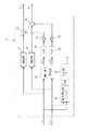
図4は、本発明の第1実施形態に係る信号処理回路9の機能ブロック図である。
図4に示すように、本実施形態の信号処理回路9は、電力算出部18、比較部19、補正信号算出部20、フィルタ21,22、スケーリング部23,24、加減算器25,26及び遅延部27,28を含む。
[Configuration of signal processing circuit]
FIG. 4 is a functional block diagram of the
As shown in FIG. 4, the
本実施形態では、上記電力算出部18、比較部19及び補正信号算出部20が、パワーアンプ16の出力電力を増加方向にシフトさせるための、変調波信号のIQベースバンド信号に対する調整信号(補正信号ΔI,ΔQ)を生成する信号生成部を構成している。
また、加減算器25,26は、生成された調整信号(補正信号ΔI,ΔQ)をこれと対応するIQベースバンド信号に重畳する信号入力部を構成している。
In the present embodiment, the
The adders /
電力算出部18は、入力側のI信号とQ信号(Iin,Qin)の2乗和よりIQベースバンド信号の瞬時電力Pを算出する。また、比較部19は、算出された瞬時電力Pと所定の閾値Pthを比較し、瞬時電力Pがその閾値Pthよりも小さい場合に、補正信号算出部20に算出指令を発する。
補正信号算出部20は、比較部19から算出指令を受けると、次の式に基づいて、Iin信号とQin信号に印加すべき補正信号ΔI,ΔQをそれぞれ算出し、これを出力する。なお、補正信号算出部20は、算出指令を受けない場合にはゼロを出力する。
The
When receiving the calculation command from the
なお、次式において、SQRT(・)は、括弧内の変数の平方根を取る関数である(以下、同様)。
ΔI={1−SQRT(Pth/P)}×Iin
ΔQ={1−SQRT(Pth/P)}×Qin
In the following equation, SQRT (•) is a function that takes the square root of a variable in parentheses (hereinafter the same).
ΔI = {1−SQRT (Pth / P)} × Iin
ΔQ = {1−SQRT (Pth / P)} × Qin
補正信号算出部20が出力した補正信号ΔI,ΔQは、それぞれ、後段のローパスフィルタやFIRフィルタ等よりなるフィルタ21,22によって帯域制限(ノーズシェーピング)され、更にその後段のスケーリング部23,24によって振幅調整されて、加減算器25,26に入力される。
また、加減算器25,26の前段にある遅延部27,28は、電力算出部18や補正信号算出部20等における演算処理の時間だけ、Iin信号とQin信号の時間を遅延させる。
The correction signals ΔI and ΔQ output from the correction
Further, the
そして、加減算器25,26は、遅延されたIin信号とQin信号から補正信号ΔI,ΔQをそれぞれ減算し、Iout信号(=SQRT(Pth/P)×Iin)とQout信号(=SQRT(Pth/P)×Qin)を出力する。
この減算により、瞬時電力Pが閾値Pth未満のIQベースバンド信号については、閾値Pth相当の瞬時電力の信号に補正される。また、瞬時電力Pが閾値Pth以上のIQベースバンド信号については、補正されずにそのまま出力される。
The adders /
By this subtraction, an IQ baseband signal having an instantaneous power P less than the threshold value Pth is corrected to an instantaneous power signal corresponding to the threshold value Pth. Further, an IQ baseband signal whose instantaneous power P is equal to or greater than the threshold value Pth is output without being corrected.
図5は、上記信号処理を行った場合のIQベースバンド信号と閾値Pthとの関係を示すIQ平面の座標図である。
この図5に示すように、本実施形態の信号処理回路9による処理は、IQベースバンド信号の瞬時電力Pの外周側をカットする従来のクリッピング処理とは逆に、その瞬時電力Pの内側をカットするいわば「くり抜き処理」を行うものである。なお、かかる「くり抜き処理」の場合も、電力が底上げされて電力増幅回路5に入力する変調波信号のPAPRが低下するので、この点においてもパワーアンプ16の電力効率が向上する。このくり抜き処理は、瞬時電力Pを所定の閾値Pth以上に底上げするという意味で、「ブースティング処理」と表現することもできる。
FIG. 5 is a coordinate diagram on the IQ plane showing the relationship between the IQ baseband signal and the threshold value Pth when the above signal processing is performed.
As shown in FIG. 5, the processing by the
〔パワーアンプの電力効率特性との関係〕
図6は、前記電力増幅回路5のパワーアンプ16の電力効率特性を示すグラフである。
図6に示すように、ET方式の電力増幅回路5の場合には、パワーアンプ16の電力効率特性は、出力電力PRFが増大するほど電力効率ηがほぼ単調に増加する単調増加区間Z1と、電力効率ηの増大が出力電力PRFにほぼ影響しない定常区間Z2とが現れるようになっている。なお、図6では、区間Z1の電力効率ηの特性を模式的に直線で示しているが、その特性は、厳密には直線ではなく、上方にやや膨らんだ曲線状になる。
[Relationship with power efficiency characteristics of power amplifier]
FIG. 6 is a graph showing the power efficiency characteristics of the power amplifier 16 of the
As shown in FIG. 6, in the case of the ET type
ここで、パワーアンプ16の出力電力(平均電力)をPRF、ドレイン側の直流電力をPDC、信号処理回路9における補正信号ΔI,ΔQの印加によってパワーアンプ16の出力側に生じる増加電力(平均電力)をPa、単調増加区間Z1における傾きをαとする。
そして、IQベースバンド信号の瞬時電力PがP<Pthである場合の、信号処理回路9による処理前の電力効率をη1、処理後の電力効率をη2とすると、これらの効率η1,η2は、それぞれ次のように算出される。
Here, the output power (average power) of the power amplifier 16 is P RF , the DC power on the drain side is P DC , and the increased power generated on the output side of the power amplifier 16 by applying the correction signals ΔI and ΔQ in the signal processing circuit 9 ( Average power) is Pa, and the slope in the monotonically increasing section Z1 is α.
When the instantaneous power P of the IQ baseband signal is P <Pth, when the power efficiency before the processing by the
η1=α×(PRF/PDC)
η2=α×{(PRF+Pa)/PDC}
一方、上記増加電力Paは、変調波信号に基づかない余分な出力であるから、信号処理後の真の電力効率η3は、η2からPaによる影響を差し引く必要がある。従って、信号処理後の真の電力効率η3は次のようになる。
η3=η2−Pa/PDC
=η1×〔1+{(α−1)/α}×(Pa/PRF)〕
η1 = α × (P RF / P DC )
η2 = α × {(P RF + Pa) / P DC }
On the other hand, since the increased power Pa is an extra output not based on the modulated wave signal, the true power efficiency η3 after the signal processing needs to subtract the influence of Pa from η2. Therefore, the true power efficiency η3 after the signal processing is as follows.
η3 = η2-Pa / P DC
= Η1 × [1 + {(α-1) / α} × (Pa / P RF )]
この場合、単調増加区間Z1の傾きαが、α>1であれば、η3がη1よりも大きくなり、信号処理回路9において補正信号ΔI,ΔQを印加したことによって、パワーアンプ16の電力効率がその印加前より改善することになる。なお、ET方式に用いるパワーアンプ16では、傾きαを10程度に設定可能である。
そこで、本実施形態の送信機3では、α>1のパワーアンプ16を電力増幅回路5に搭載している。
In this case, if the slope α of the monotonically increasing section Z1 is α> 1, η3 becomes larger than η1, and the correction signal ΔI, ΔQ is applied in the
Therefore, in the
上記構成に係る本実施形態の信号処理回路9によれば、前記くり抜き処理によってIQベースバンド信号が所定の閾値Pth未満になることがないので(図5参照)、パワーアンプ16の出力電力が増加電力Pa未満に落ち込むことがない(図6参照)。
そして、上記の通り、パワーアンプ16の単調増加区間Z1における傾きαが、1より大きくなっているので、パワーアンプ16の電力効率を信号処理前に比べて向上することができる。
According to the
As described above, since the slope α of the power amplifier 16 in the monotonically increasing section Z1 is greater than 1, the power efficiency of the power amplifier 16 can be improved as compared with that before the signal processing.
〔第2実施形態〕
図7は、本発明の第2実施形態に係る信号処理回路9の機能ブロック図である。
本実施形態の信号処理回路9は、所定の正弦波信号S1又は合成波信号S2を生成する信号生成部としてのオフセット回路30と、その正弦波信号S1又は合成波信号S2をIQベースバンド信号に重畳する信号入力部としての加算器31,32とから構成されている。
[Second Embodiment]
FIG. 7 is a functional block diagram of the
The
図8(a)は、上記正弦波信号S1のパワースペクトルを示し、図8(b)は、上記合成波信号S2のパワースペクトルを示している。
図8(a)に示すように、正弦波信号S1は、マルチキャリア信号よりなる変調波信号(本実施形態ではOFDM信号)におけるDCサブキャリアに対応する周波数の正弦波よりなる。なお、DCサブキャリアはデータ伝送に用いないので、これに対応する周波数の正弦波信号S1をIQベースバンド信号に重畳しても、受信側において通信不良が生じることはない。
FIG. 8A shows the power spectrum of the sine wave signal S1, and FIG. 8B shows the power spectrum of the combined wave signal S2.
As shown in FIG. 8A, the sine wave signal S1 is composed of a sine wave having a frequency corresponding to a DC subcarrier in a modulated wave signal (OFDM signal in the present embodiment) composed of a multicarrier signal. Since the DC subcarrier is not used for data transmission, communication failure does not occur on the receiving side even if a sine wave signal S1 having a frequency corresponding to the DC subcarrier is superimposed on the IQ baseband signal.
また、図8(b)に示すように、合成波信号S2は、マルチキャリア信号よりなる変調波信号におけるサブキャリアf1,f2,……fnの中心周波数に対応する正弦波信号を合成したものである。
なお、合成波信号S2は、各サブキャリアの中心周波数に対応する周波数の正弦波信号を合成したものであるから、これをIQベースバンド信号に重畳してもその位相が変化せず、受信側で通信不良が生じることはない。
Further, as shown in FIG. 8B, the synthesized wave signal S2 is a synthesized sine wave signal corresponding to the center frequency of the subcarriers f1, f2,... Fn in the modulated wave signal composed of the multicarrier signal. is there.
Since the synthesized wave signal S2 is a synthesized sine wave signal having a frequency corresponding to the center frequency of each subcarrier, the phase does not change even if it is superimposed on the IQ baseband signal. No communication failure occurs.
また、図8(b)では、合成波信号S2がすべてのサブキャリアf1,f2,……fnの中心周波数に対応する周波数成分を有しているが、そのうちの一部のサブキャリアだけを使用するものであってもよい。
本実施形態では、上記正弦波信号S1や合成波信号S2がIQベースバンド信号に重畳されるので、その信号S1,S2の印加によってパワーアンプ16の出力電力が増加方向にシフトし、その出力電力がゼロに落ち込むことがない。このため、本実施形態においても、第1実施形態と同様の作用効果が得られる。
In FIG. 8B, the synthesized wave signal S2 has frequency components corresponding to the center frequencies of all the subcarriers f1, f2,... Fn, but only some of the subcarriers are used. You may do.
In the present embodiment, since the sine wave signal S1 and the synthesized wave signal S2 are superimposed on the IQ baseband signal, the output power of the power amplifier 16 is shifted in the increasing direction by the application of the signals S1 and S2, and the output power is increased. Never falls to zero. For this reason, also in this embodiment, the same operation effect as a 1st embodiment is acquired.
また、本実施形態では、第1実施形態(図4)の信号処理回路9のような、電力算出部18や補正信号算出部19等の演算処理部が不要であるから、回路構成が簡素となり、低コスト化を図れるという利点もある。
Further, in the present embodiment, the circuit configuration is simplified because an arithmetic processing unit such as the
〔第3実施形態〕
図9は、本発明の第3実施形態に係る信号処理回路9の機能ブロック図である。
図9に示すように、本実施形態の信号処理回路9では、第1補正信号算出部20に加えて、IQベースバンド信号に対してクリッピング処理を行うための第2補正信号算出部34を設けている点が、第1実施形態(図4)の信号処理回路9と異なる。
以下、第1実施形態(図4)と同じ機能部については、図9に同一符号を付して説明を省略し、相違点に係る構成ついて重点的に説明する。
[Third Embodiment]
FIG. 9 is a functional block diagram of a
As shown in FIG. 9, in the
Hereinafter, the same functional units as those in the first embodiment (FIG. 4) will be denoted by the same reference numerals in FIG.
比較部19は、小さい方の第1閾値Pth1と大きい方の第2閾値Pth2の2つの閾値を保持しており、第1閾値Pth1は第1実施形態(図4)の閾値Pthと同じ値である。
また、比較部19は、算出された瞬時電力Pと各閾値Pth1,Pth2を比較し、瞬時電力Pが第1閾値Pth1よりも小さい場合には、第1補正信号算出部20に算出指令を発するとともに、瞬時電力Pが第2閾値Pth2よりも大きい場合には、第2補正信号算出部34に算出指令を発する。
The
The
この場合、第1補正信号算出部20が出力する第1補正信号ΔI1,ΔQ1は、第1実施形態の場合と同様に、次式によって算出される。
ΔI1={1−SQRT(Pth1/P)}×Iin
ΔQ1={1−SQRT(Pth1/P)}×Qin
In this case, the first correction signals ΔI1 and ΔQ1 output from the first correction
ΔI1 = {1−SQRT (Pth1 / P)} × Iin
ΔQ1 = {1−SQRT (Pth1 / P)} × Qin
一方、第2補正信号算出部34は、比較部19から算出指令を受けると、次の式に基づいて、Iin信号とQin信号に印加すべき第2補正信号ΔI2,ΔQ2をそれぞれ算出し、これを出力する。なお、第2補正信号算出部34は、算出指令を受けない場合にはゼロを出力する。
ΔI2={1−SQRT(Pth2/P)}×Iin
ΔQ2={1−SQRT(Pth2/P)}×Qin
On the other hand, when receiving the calculation command from the
ΔI2 = {1−SQRT (Pth2 / P)} × Iin
ΔQ2 = {1-SQRT (Pth2 / P)} × Qin
第2補正信号算出部34が出力した第2補正信号ΔI2,ΔQ2は、それぞれ、後段のローパスフィルタやFIRフィルタ等よりなるフィルタ35,34によって帯域制限(ノーズシェーピング)され、更にその後段のスケーリング部37,38によって振幅調整されて、加減算器25,26に入力される。
The second correction signals ΔI2 and ΔQ2 output from the second correction
そして、加減算器25,26は、遅延されたIin信号とQin信号から第2補正信号ΔI2,ΔQ2をそれぞれ減算し、Iout信号(=SQRT(Pth2/P)×Iin)とQout信号(=SQRT(Pth2/P)×Qin)を出力する。
この減算により、瞬時電力Pが第2閾値Pth2を超えるIQベースバンド信号については、第2閾値Pth2相当の瞬時電力の信号に補正される。また、瞬時電力Pが第2閾値Pth2以下のIQベースバンド信号については、補正されずにそのまま出力される。
Then, the adder /
By this subtraction, an IQ baseband signal whose instantaneous power P exceeds the second threshold value Pth2 is corrected to a signal of instantaneous power equivalent to the second threshold value Pth2. In addition, an IQ baseband signal whose instantaneous power P is equal to or less than the second threshold value Pth2 is output as it is without being corrected.
図10は、第3実施形態の信号処理回路9の場合のIQベースバンド信号と第1及び第2閾値Pth1,Pth2との関係を示すIQ平面の座標図である。
この図10に示すように、本実施形態の信号処理回路9による処理は、IQベースバンド信号の瞬時電力Pの内側をカットする前記くり抜き処理と、そのIQベースバンド信号の瞬時電力Pの外周側をカットするクリッピング処理との双方を行うものである。
FIG. 10 is a coordinate diagram on the IQ plane showing the relationship between the IQ baseband signal and the first and second threshold values Pth1 and Pth2 in the case of the
As shown in FIG. 10, the processing by the
このため、くり抜き処理のみを行う第1実施形態(図4)の信号処理回路9に比べて、電力増幅回路5に入力する変調波信号のPAPRを更に低下させることができ、パワーアンプ16の電力効率をより向上することができる。
Therefore, compared with the
〔その他の変形例〕
今回開示した実施形態は例示であって制限的なものではない。本発明の権利範囲は特許請求の範囲によって示され、特許請求の範囲の構成と均等の範囲内での全ての変更が含まれる。
例えば、本発明の信号処理回路9とその後段の電力増幅回路5は、基地局装置1だけでなく、この基地局装置1とCPRI(Common Public Radio Interface)で繋がるRRH(Remote Radio Head)に搭載することもできる。
[Other variations]
The embodiment disclosed this time is illustrative and not restrictive. The scope of the present invention is defined by the terms of the claims, and includes all modifications that are within the scope of the claims and equivalents.
For example, the
また、本発明の信号処理回路9は、ET方式の電力増幅回路5だけでなく、EER(Envelope Elimination and Restoration)方式の電力増幅回路に適用することもできる。
もっとも、EER方式では、RF信号には振幅変動がなく、包絡線信号に振幅変動があるので、EER方式の電力増幅回路に本発明を適用する場合には、その包絡線信号に本発明の信号処理を施して当該電力増幅回路の効率改善を図ることになる。
The
However, in the EER system, there is no amplitude fluctuation in the RF signal, and there is an amplitude fluctuation in the envelope signal. Therefore, when the present invention is applied to an EER power amplifier circuit, the signal of the present invention is included in the envelope signal. Processing is performed to improve the efficiency of the power amplifier circuit.
1 基地局装置
2 移動端末
3 送信機
4 送信用プロセッサ
5 電力増幅回路
9 信号処理部(信号処理回路)
16 パワーアンプ
18 電力算出部(信号生成部)
19 比較部(信号生成部)
20 補正信号算出部(信号生成部)
21,22 フィルタ
23,24 スケーリング部
25,26 加減算器(信号入力部)
27,28 遅延部
30 オフセット回路(信号生成部)
31,32 加算器(信号入力部)
34 第2補正信号算出部
35,36 フィルタ
37,38 スケーリング部
DESCRIPTION OF SYMBOLS 1 Base station apparatus 2
16
19 Comparison unit (signal generation unit)
20 Correction signal calculation unit (signal generation unit)
21, 22
27, 28
31, 32 adder (signal input unit)
34 Second correction
Claims (7)
前記パワーアンプの出力電力を増加方向にシフトさせるための、前記電力増幅回路に入力される前記変調波信号のIQベースバンド信号に対する調整信号を生成する信号生成部と、
生成された前記調整信号を前記IQベースバンド信号に重畳する信号入力部と、
を備える信号処理回路。 A signal processing circuit for improving the power efficiency of a power amplifier included in a power amplifier circuit for amplifying a modulated wave signal,
A signal generator for generating an adjustment signal for an IQ baseband signal of the modulated wave signal input to the power amplifier circuit for shifting the output power of the power amplifier in an increasing direction;
A signal input unit that superimposes the generated adjustment signal on the IQ baseband signal;
Bei obtain signal processing circuit.
前記パワーアンプの出力電力を増加方向にシフトさせるための、前記変調波信号のIQベースバンド信号に対する調整信号を生成する信号生成部と、
生成された前記調整信号を前記IQベースバンド信号に重畳する信号入力部と、
を備え、
前記信号生成部は、前記IQベースバンド信号の瞬時電力を算出する電力算出部と、前記瞬時電力が所定の閾値より小さい前記IQベースバンド信号を、当該閾値相当の瞬時電力となるように補正するための補正信号を算出する信号算出部と、を有しており、
前記信号入力部は、前記補正信号よりなる前記調整信号を前記IQベースバンド信号に重畳する信号処理回路。 A signal processing circuit for improving the power efficiency of a power amplifier included in a power amplifier circuit for amplifying a modulated wave signal,
A signal generator for generating an adjustment signal for the IQ baseband signal of the modulated wave signal for shifting the output power of the power amplifier in an increasing direction;
A signal input unit that superimposes the generated adjustment signal on the IQ baseband signal;
With
The signal generator corrects the IQ baseband signal whose instantaneous power is smaller than a predetermined threshold so that the instantaneous power of the IQ baseband signal is equal to the threshold. A signal calculation unit for calculating a correction signal for
The signal input unit, the correction signal consisting of said adjustment signal to the IQ baseband signal signal processing circuit you superimposed.
前記信号入力部は、前記第2の補正信号を前記IQベースバンド信号に重畳する請求項2に記載の信号処理回路。 The signal generation unit calculates a second correction signal for correcting the IQ baseband signal in which the instantaneous power is larger than a predetermined second threshold so that the instantaneous power is equivalent to the second threshold. A second signal calculating unit;
The signal processing circuit according to claim 2 , wherein the signal input unit superimposes the second correction signal on the IQ baseband signal.
前記信号入力部は、前記正弦波信号よりなる前記調整信号を前記IQベースバンド信号に重畳する請求項1〜3のいずれか1項に記載の信号処理回路。 The signal generation unit includes an offset circuit that generates a sine wave signal having a frequency corresponding to a DC subcarrier of the modulated wave signal including a multicarrier signal,
The signal input unit, a signal processing circuit according to any one of claims 1 to 3, superimposing the adjustment signal consisting of the sine wave signal to the IQ baseband signal.
前記パワーアンプの出力電力を増加方向にシフトさせるための、前記変調波信号のIQベースバンド信号に対する調整信号を生成する信号生成部と、
生成された前記調整信号を前記IQベースバンド信号に重畳する信号入力部と、
を備え、
前記信号生成部は、マルチキャリア信号よりなる前記変調波信号の複数のサブキャリアの中心周波数に対応する周波数の正弦波信号を合成した合成波信号を生成するオフセット回路よりなり、
前記信号入力部は、前記合成波信号を前記調整信号として前記IQベースバンド信号に重畳する信号処理回路。 A signal processing circuit for improving the power efficiency of a power amplifier included in a power amplifier circuit for amplifying a modulated wave signal,
A signal generator for generating an adjustment signal for the IQ baseband signal of the modulated wave signal for shifting the output power of the power amplifier in an increasing direction;
A signal input unit that superimposes the generated adjustment signal on the IQ baseband signal;
With
The signal generation unit includes an offset circuit that generates a synthesized wave signal obtained by synthesizing a sine wave signal having a frequency corresponding to a center frequency of a plurality of subcarriers of the modulated wave signal including a multicarrier signal,
The signal input unit, the synthesized wave signal the adjustment signal as the IQ baseband signal you superimposed signal processing circuit.
Priority Applications (1)
| Application Number | Priority Date | Filing Date | Title |
|---|---|---|---|
| JP2010018695A JP5532968B2 (en) | 2010-01-29 | 2010-01-29 | Signal processing circuit and communication apparatus having this circuit |
Applications Claiming Priority (1)
| Application Number | Priority Date | Filing Date | Title |
|---|---|---|---|
| JP2010018695A JP5532968B2 (en) | 2010-01-29 | 2010-01-29 | Signal processing circuit and communication apparatus having this circuit |
Publications (2)
| Publication Number | Publication Date |
|---|---|
| JP2011160089A JP2011160089A (en) | 2011-08-18 |
| JP5532968B2 true JP5532968B2 (en) | 2014-06-25 |
Family
ID=44591699
Family Applications (1)
| Application Number | Title | Priority Date | Filing Date |
|---|---|---|---|
| JP2010018695A Expired - Fee Related JP5532968B2 (en) | 2010-01-29 | 2010-01-29 | Signal processing circuit and communication apparatus having this circuit |
Country Status (1)
| Country | Link |
|---|---|
| JP (1) | JP5532968B2 (en) |
Families Citing this family (2)
| Publication number | Priority date | Publication date | Assignee | Title |
|---|---|---|---|---|
| JP5759920B2 (en) * | 2012-03-07 | 2015-08-05 | 株式会社日立製作所 | Wireless transmitter and envelope tracking power control method |
| US10110173B2 (en) * | 2016-10-28 | 2018-10-23 | Samsung Electro-Mechanics Co., Ltd. | Envelope tracking current bias circuit and power amplifier apparatus |
Family Cites Families (5)
| Publication number | Priority date | Publication date | Assignee | Title |
|---|---|---|---|---|
| JP2718398B2 (en) * | 1995-06-30 | 1998-02-25 | 日本電気株式会社 | CDMA base station transmitter |
| JP2003018026A (en) * | 2001-06-29 | 2003-01-17 | Taiyo Yuden Co Ltd | Radio communication method and device |
| JP4296471B2 (en) * | 2002-10-10 | 2009-07-15 | 住友電気工業株式会社 | Peak power suppression method and apparatus |
| US6987417B2 (en) * | 2003-06-24 | 2006-01-17 | Northrop Grumman Corpoation | Polar and linear amplifier system |
| EP2120335B1 (en) * | 2007-01-31 | 2015-06-10 | Panasonic Corporation | Power voltage forming device and polar modulation transmission device |
-
2010
- 2010-01-29 JP JP2010018695A patent/JP5532968B2/en not_active Expired - Fee Related
Also Published As
| Publication number | Publication date |
|---|---|
| JP2011160089A (en) | 2011-08-18 |
Similar Documents
| Publication | Publication Date | Title |
|---|---|---|
| US11245429B2 (en) | System and method for increasing bandwidth for digital predistortion in multi-channel wideband communication systems | |
| EP2909931B1 (en) | Envelope tracking distributed amplifier | |
| US9768739B2 (en) | Digital hybrid mode power amplifier system | |
| JP4272072B2 (en) | Method and apparatus for reducing transmitter peak power consumption using dual matrix | |
| KR20070116205A (en) | Systems, methods and apparatused for linear envelope elimination and restoration transmitters | |
| WO2011104951A1 (en) | Peak power suppression circuit, and communication device provided with said circuit | |
| JP5201158B2 (en) | Signal processing circuit and communication apparatus having this circuit | |
| US20150091643A1 (en) | Using Fractional Delay Computations to Improve Intermodulation Performance | |
| WO2012164951A1 (en) | Transmitter and signal processing method | |
| US20090323857A1 (en) | Configurable sub-band filtering to reduce peak-to-average power ratio of ofdm signals or the like | |
| Abi Hussein et al. | Digital predistortion for RF power amplifiers: State of the art and advanced approaches | |
| CN108347226B (en) | Envelope tracking method, system and device | |
| Helaoui et al. | Linearization of power amplifiers using the reverse MM-LINC technique | |
| JP4302436B2 (en) | Transmitter and receiver | |
| JP4836866B2 (en) | Communication device | |
| JP2008167289A (en) | Transmission apparatus | |
| JP5532968B2 (en) | Signal processing circuit and communication apparatus having this circuit | |
| KR100605826B1 (en) | Apparatus and method for improving the efficiency of power amplifier operating under a large peak-to-average ratio | |
| US8654891B2 (en) | Peak suppressing apparatus, peak suppressing method and wireless communications apparatus | |
| JP4918390B2 (en) | Transmitter | |
| JP2003046480A (en) | Peak limiter and multi-carrier amplifier | |
| JP2011160264A (en) | Signal processing circuit and communication apparatus with the same | |
| JP3714917B2 (en) | Peak limiter and multi-carrier amplifier | |
| JP5146144B2 (en) | Peak suppression device, peak suppression method, and wireless communication device | |
| JP4680077B2 (en) | OFDM communicator |
Legal Events
| Date | Code | Title | Description |
|---|---|---|---|
| A621 | Written request for application examination |
Free format text: JAPANESE INTERMEDIATE CODE: A621 Effective date: 20121220 |
|
| A977 | Report on retrieval |
Free format text: JAPANESE INTERMEDIATE CODE: A971007 Effective date: 20130711 |
|
| A131 | Notification of reasons for refusal |
Free format text: JAPANESE INTERMEDIATE CODE: A131 Effective date: 20130730 |
|
| A521 | Written amendment |
Free format text: JAPANESE INTERMEDIATE CODE: A523 Effective date: 20130903 |
|
| TRDD | Decision of grant or rejection written | ||
| A01 | Written decision to grant a patent or to grant a registration (utility model) |
Free format text: JAPANESE INTERMEDIATE CODE: A01 Effective date: 20140401 |
|
| R150 | Certificate of patent or registration of utility model |
Ref document number: 5532968 Country of ref document: JP Free format text: JAPANESE INTERMEDIATE CODE: R150 |
|
| A61 | First payment of annual fees (during grant procedure) |
Free format text: JAPANESE INTERMEDIATE CODE: A61 Effective date: 20140414 |
|
| LAPS | Cancellation because of no payment of annual fees |